structural phase transition, grain growth and optical
TRANSCRIPT
1
Structural phase transition, grain growth and optical properties of uncompensated Ga-V
co-doped TiO2
Nasima Khatun1, Saurabh Tiwari
2, Jayanti Lal
3, Chuan-Ming Tseng
4, Shun Wei Liu
5,
Sajal Biring6 and Somaditya Sen
1,2*
1Department of Physics, Indian Institute of Technology Indore, Simrol Campus, Khandwa Road,
Indore 453552, India
2Metallurgy Engineering and Material Sciences, Indian Institute of Technology Indore, Simrol
Campus, Khandwa Road, Indore 453552, India
3Department of chemistry, Vels Institute of Science, Technology & Advanced Studies, Chennai,
Tamil Nadu – 600117, India
4Department of Materials Engineering, Ming Chi University of Technology, New Taipei City -
24301, Taiwan
5Organic Electronic Research Center, Ming Chi University of Technology, New Taipei City -
24301, Taiwan
6Electronic Engg., Ming Chi University of Technology, New Taipei City -24301, Taiwan
Abstract
Effect of uncompensated Ga-V co-doping (0≤x≤0.046) on structural phase transition, grain
growth process and optical properties of TiO2 is reported here. Inhibition of phase transition due
to co-doping is confirmed by X-ray diffraction measurement. Activation energy of phase
transition increases from 120KJ/mol (x=0) to 140 KJ/mol (x=0.046) due to Ga-V co-doping. In
anatase phase, lattice constants increase by the effect of Ga3+
interstitials. This results in
inhibition of phase transition. Anatase phase becomes stable up to ~650 C in co-doped sample
whereas for pure TiO2 phase transition starts in between 450-500 ⁰C. In anatase phase, strain
increases due to co-doping which reduces crystallite size. In rutile phase, grain growth process is
enhanced due to co-doping and particles show a rod-like structure with majority {110} facets.
Bandgap decreases in both phases and reduced to a visible light region. BET analysis shows that
surface area increases from 4.55 m2/g (x=0) to 96.53 m
2/g (x=0.046) by Ga-V incorporation
which provide a large number of active site for photocatalytic activity. Hence, co-doped anatase

2
nanoparticle can be used as a promising candidate for photocatalytic applications using visible
light up to a higher temperature ~650 C.
Introduction:
TiO2 is of continual interest due to its multifunctional properties. Different crystal structure and
corresponding electronic band structure facilitate its applications in different fields such as in
opto-electronic devices1, 2
, self-cleaning glass coating materials3, photocatalyst
4, 5, fuel cell
6,
dye-sensitized solar cell7, 8
, opacifier and white pigment9, 10
, etc.. It facilitates environmentally
beneficial reactions through photocatalytic activity by splitting of water to generate hydrogen
and treatment of polluted air and water 11
. Low cost, nontoxicity, and high chemical stability add
a special importance for application.
TiO2 has three naturally occurring polymorph12
. In order of abundance, these are rutile (R),
anatase (A), and brookite (B)13
. At lower temperature anatase is the most stable phase due to its
low surface free energy 14, 15
. Pure brookite phase is not available at normal ambient condition
due to its complex crystal structure. Both anatase and brookite are metastable phases. With
increasing temperature ( 750 C) both the phases are irreversibly transformed into stable rutile
phase16
. Density functional theory (DFT) calculation showed that effective mass of electrons and
holes is smaller in anatase phase compared to brookite and rutile phases17
. This facilitates the
migration of carriers and enhances photocatalytic activity. Due to lighter effective mass, smaller
particle size (highly stable 10-15 nm)12, 18
and longer lifetime of photogenerated charge
carriers17
, anatase is an active polymorph for photocatalytic applications than brookite and
rutile19-21
.
In spite of these important properties of anatase TiO2, there are few restraints. Anatase TiO2 has
lower thermal stability ( 450-500 C) and wide bandgap (3.2 eV)22
. Due to its wide bandgap, it
only absorbs ~5% radiation of the solar spectrum. The entire visible region (~45%) remains
unutilized. From a practical application point of view, utilization of visible light is beneficial.
Therefore, people have made significant efforts to shift its phase transition temperature to a
higher temperature region and tune the bandgap of TiO2 in visible light range. Different
processes have been adapted for this purpose. These include synthesis methods 23-25
, strain26, 27
,
doping with different elements (Fe, Mo, V, Ru, Cu, Fe, Cr etc.) 14, 28-32
, etc.

3
Among all these processes, doping is the easiest way to control phase transition and thereby
properties (tune the bandgap). From the literature, it was observed that Ga doping inhibits the
phase transition and play a robust role in photocatalytic activity (PCA) in UV region33, 34
.
Vanadium considerably reduces the bandgap but promotes phase transition 16, 35, 36
. Hence, in this
context uncompensated Gallium and Vanadium co-doping have been chosen to overcome both
the problem. Here in this work, effect of uncompensated Ga-V co-doping on structural phase
transition, grain growth process and optical properties of TiO2 has been discussed.
Experimental
Ga and V co-doped TiO2 (Ti(1-x)( Ga0.8V0.2)xO2: TGV) nanoparticles (with x=0.00 (TGV0), 0.015
(TGV1), 0.031 (TGV3) and 0.046 (TGV4)) are prepared by modified sol-gel synthesis. The Ti-
solution is prepared by mixing required amount of dihydoxy-bis titanium (TALH: C6H18N2O8Ti)
in deionized (DI) water at room temperature. An appropriate amount of Ga(NO3)3 is dissolved in
DI water in one beaker. In another beaker, V2O5 is also dissolved in DI water by adding little
amount of NH4OH while stirring. Both the solutions are added dropwise into a Ti-solution.
After 1h of mixing, citric acid and ethylene glycol is added to it. This mixture is stirred for
another 1h for homogeneous mixing. Thereafter it is slowly heated. Temperature of this solution
is maintained at 80 ⁰C for 4-5h to get the thick gel. The gel is burnt on a hot plate at 100 ⁰C in
normal ambient condition resulting in a black dry powder. This powder is denitrified and
decarburized at 450 ⁰C in an air atmosphere for 6h to get desired nanoparticles. The collected
powder is subsequently heated at eight different temperatures in 50 ⁰C steps from 450 ⁰C to 800
⁰C, stabilizing for 6h at each temperature.
Thermal gravimetric analysis (TGA) was performed to estimate the crystallization temperature
of the samples by METTLER TOLEDO (TGA/DSC 1) system using the STARe software system
up to 800 ⁰C in an air atmosphere with a heating rate of 5 ⁰C min-1
. Structural analysis was
studied by powder X-ray diffraction (XRD) patterns using Bruker D2 phaser diffractometer with
Cu-Kα radiation (λ=1.5418 Å). Morphology and particle size were investigated using high-
resolution transmission electron microscope (HRTEM) (JEOL JEM-2100 LaB6, accelerating
voltage - 200 kV) and field emission scanning electron microscopy (Supra55 Zeiss- FESEM).
Surface area of the samples was calculated by Brunauer–Emmett–Teller (BET) measurement.

4
Diffuse reflectance spectroscopy (DRS) measurements were carried out using Bentham TMc300
Monochromator to estimate the changes in the bandgap.
Results and Discussion
TGA measurement on dry gel powder (TGV0) is performed from room temperature (RT-27 C)
to 800 C. Weight loss of 1.04%, from RT to ~110 °C, is observed in pure TiO2 (TGV0) (Fig. 1).
This is due to elimination of physically adsorbed water37
. In the temperature regime, ~110 to 315
°C a sharper weight loss of 2.52% is observed. This may be attributed to the rupture of a
polymeric chain of black powder and removal of ethylene glycol units38
. A final very sharp
weight loss of 5.61% is observed in the temperature regime ~315 to 430 C. This drastic loss is
due to decomposition of the organic compounds into carbon dioxide and nitrogen dioxide,
desorption of chemisorbed water molecules39, 40
. This temperature is well enough to consume
unreacted precursor and thereby form well crystalline samples. Note that beyond ~430-450 C,
there is almost no change in weight loss. Thus, 450 ⁰C is selected as the optimum calcination
temperature which is high enough to achieve crystallization, and optimum to reduce the thermal
growth of the particles to maintain nano-scale features in the calcined powder. A minor weight
loss of 0.48%, in between 550 to 650 °C can be ascribed to the removal of the surface hydroxyls
present in the samples41
.
Fig. 1 TGA curve of the TGV0 sample at a temperature range of 27-800 C.
HRTEM is a very powerful tool to investigate a particle in a very small range (around 1-2 nm). It
gives crystallographic information and clear morphology of the nanoparticles. Fig. 2 (a and c)
shows the TEM images of TGV0 and TGV3 samples. Almost spherical shape particles are
observed for both the samples. Particles size of both the sample has been calculated using Image

5
J software. Histogram of TGV0 and TGV3 sample (inset of Fig. 2(a) and (c)) shows average
particles size are in the range of ~12-15 nm and ~8-10 nm respectively. It is observed that
particle size reduces due to co-doping. In V doped TiO2, it was observed that crystallite size
reduced with doping 35, 42
. Ga doping also reduces crystallite size21, 33
. Hence, a combination of V
and Ga co-doping is supposed to reduce crystallite size. TEM results confirm the same. In most
cases, strain increases upon doping of foreign elements into TiO2 and this strain hinders the grain
growth process of nanoparticles. From HRTEM images, it is observed that d spacing of lattice
fringes of both the samples are ~0.35 nm which corresponds to 101 planes of anatase TiO2 (Fig.
2 (b: TGV0 and d:TGV3). Clarity of the fringes signifies both the samples are well crystalline.
Such a good crystallinity at a low temperature ~450 C, is possible due to proper choice of
specific reagents (ethylene glycol and citric acid)43, 44
used in this synthesis methods. The ring-
like SAED patterns (inset of Fig. 2 (b: TGV0 and d: TGV3) reveals the polycrystalline nature
and confirms anatase phase of TiO2 of both the samples.

6
Fig. 2: TEM images of TGV0 (a) and TGV3 (c) and inset shows the histogram of particle size
distribution of corresponding samples. (b and d) HRTEM images of TGV0 and TGV3 and insets
show SAED pattern of corresponding samples.
Table 1. BET surface area, pore diameter, pore volume of Ga-V co-doped TiO2 samples.
Sample
name
BET surface area
(m2/g)
Pore diameter
(nm)
Pore volume
(cm3/g)
TGV0 4.55 3.819 0.009
TGV1 53.95 3.823 0.044
TGV3 85.25 3.826 0.060
TGV4 96.53 3.829 0.061

7
Nitrogen adsorption/desorption isotherms (Fig. 3) of all the samples display type IV isotherms
according to IUPAC classification. Hysteresis loop of the isotherms are of typical H2(a) type45
.
BET surface area increases from 4.55 m2/g (TGV0) to 96.53 m
2/g (TGV4). Surface area depends
on size and morphology of nanoparticles. Smaller the size, larger is the surface area of
nanoparticles. Hence, as BET surface area increases with doping a reduction in crystallite size is
expected. Pore size distribution is calculated from BJH method on the desorption isotherms (Fig.
3(e-h)). Pores sizes for all samples are <4 nm. Mesoporous materials have pore diameters
ranging from 2-nm to 50nm 45
. Hence, these samples can be classified as mesoporous materials
based on the pore diameter and nature of hysteresis loop. A larger surface area due to Ga-V
incorporation provides a large number of active sites which makes the materials better for PCA.
Fig. 3 (a-d) Nitrogen adsorption/desorption isotherms of TGV samples (450 ⁰C) and (e-h)
Barrett-Joyner Halenda (BJH) pore size distribution curve of the samples.
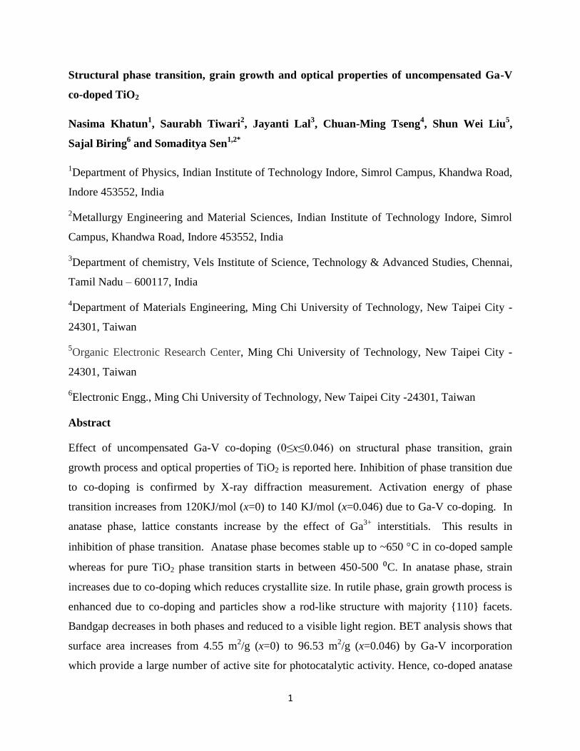
XRD pattern for all samples (TGV0, TGV1, TGV3, and TGV4), heated at temperatures ~450 C,
500 C, 550 C, 600 C, 650 C, 700 C, 750 C, and 800 C, are shown in Fig. 4. XRD pattern
for all TGV samples heated at 450 ⁰C for 6h (Fig. 4(a)) matches well with COD ID-9015929
which is of tetragonal anatase phase of TiO2 having space group I41/amd. Hence, all the samples
are in pure anatase phase. There are no traces of any rutile phase at this temperature. Also, there
is no evidence of any simple or complex metal oxide phases related to Ti, Ga, and V. With
increasing temperature the anatase phase of TGV samples gradually starts to convert to a rutile
phase and forms a mixed phase. Further heating at a higher temperature (~800 ⁰C), all the TGV

8
samples are converted into an entire rutile phase. XRD patterns of TGV samples (800 ⁰C),
matches well with COD ID-9009083 which is of tetragonal rutile phase of TiO2 having space
group P42/mnm. The samples heat treated between 450-800 ⁰C shows mixed phase of anatase
and rutile.
Fig. 4 XRD patterns of all TGV samples at eight different temperatures (450-800 C) in the
range of 2θ=20-80.
For pure TiO2 (TGV0), AR phase transformation starts in between ~450-500 C. Phase
transition at this particular temperature happens due to the choice of specific reagent (ethylene
glycol and citric acid)43
used in this method. Complete transformation into rutile phase is
observed at ~750 C. In case of co-doped (Ga-V) samples, no trace of rutile phase has been
detected below ~550 C. For TGV1 and TGV3, AR phase transition starts ~550-600 C. For
TGV4, AR phase transition starts at ~650-700 C. A complete conversion into rutile phase
happens at ~800 C. It is observed from these XRD spectra that the appearance of rutile phase
and complete conversion into rutile phase both are shifted to higher temperature with increasing

9
doping concentration. Hence, Ga and V co-doping into TiO2 inhibits the phase transition or
stabilize the anatase phase to a higher temperature (for TGV1 and TGV3 up to ~550 C while for
TGV4 up to ~650 C).
Vigilant investigation on XRD patterns of the samples at rutile phase (800 ⁰C) shows small
appearance of -Ga2O3 phase for TGV3 and TGV4 samples (provided in supplementary file Fig.
S1) which matches with COD ID-2004987 (-Ga2O3). However, in anatase phase, such type of
impurity has not been detected. Anatase phase has some inherent empty space inside crystal
structure46
. Therefore Ga and V easily incorporated into TiO2 lattice and occupy the position of
interstitials and substitutional sites. Density () of rutile phase (4.25 gm/cm3) is higher than
anatase (3.89 gm/cm3)14
. Hence, rutile phase has less empty space compared to anatase phase. As
Ga3+
(0.76Å) ion has slightly bigger ionic radius compared to both Ti4+
(0.745Å) and V5+/4+
(0.68Å/0.72Å), therefore at higher temperature due to thermal instability and less space, Ga3+
ions move out from TiO2 lattice and segregate on the surface of the particles. These Ga ions at
higher temperature react with environment oxygen and form -Ga2O3 which are highly dispersed
on the surface of particles. -Ga2O3 is a stable crystalline form of gallium oxide at a higher
temperature (650 C)33
.
Rutile phase fraction (fR) in the mixed phases is estimated at different temperatures using Spurr
and Mayers equation 47
. Temperature dependence of fR (Fig. 5) for co-doped samples ensures an
inhibition of phase transformation with increasing doping concentration. All processing
parameters (like heating/cooling rates, environment of calcination, etc.) are kept constant. Hence,
this inhibition of phase transformation entirely depends on the concentration of Ga and V co-
doping. In general, oxygen vacancy results in lattice contraction and promotes AR phase
transition. On the other hand, interstitials expand the lattice and thereby inhibits the phase
transition48
. Ga ion has slightly bigger ionic (VI-0.76Å) radius and lesser charge +3 compared to
Ti4+
(VI-0.745Å), while V has variable charge states (3+,4+,5+) with ionic radius (V3+
(VI-
0.78Å), V4+
(VI-0.72Å), and V5+
(VI-0.68Å)). From literature, it was observed that charge states
and ionic radius are very sensitive to accelerate and delay the AR phase transition14
. Ga and V
ions have different charge states. Total charge compensation can only happen if amount of Ga
and V are equal and the entire V-population is in V5+
state. Ga: V ratio in all the samples is 4:1.
Hence, for charge compensation, it either creates oxygen vacancies or form interstitials. As
10
discussed above, interstitials are responsible for inhibition of phase transitions and XRD results
show inhibition of phase transition due to co-doping. This hints that effect of interstitials is more
prominent compared to oxygen vacancies.
Fig. 5 XRD pattern of all TGV samples at eight different temperature (~450-800 C) in the range
of 2θ=24.5-28. (b) Fraction of rutile phase (fR) at different temperature.
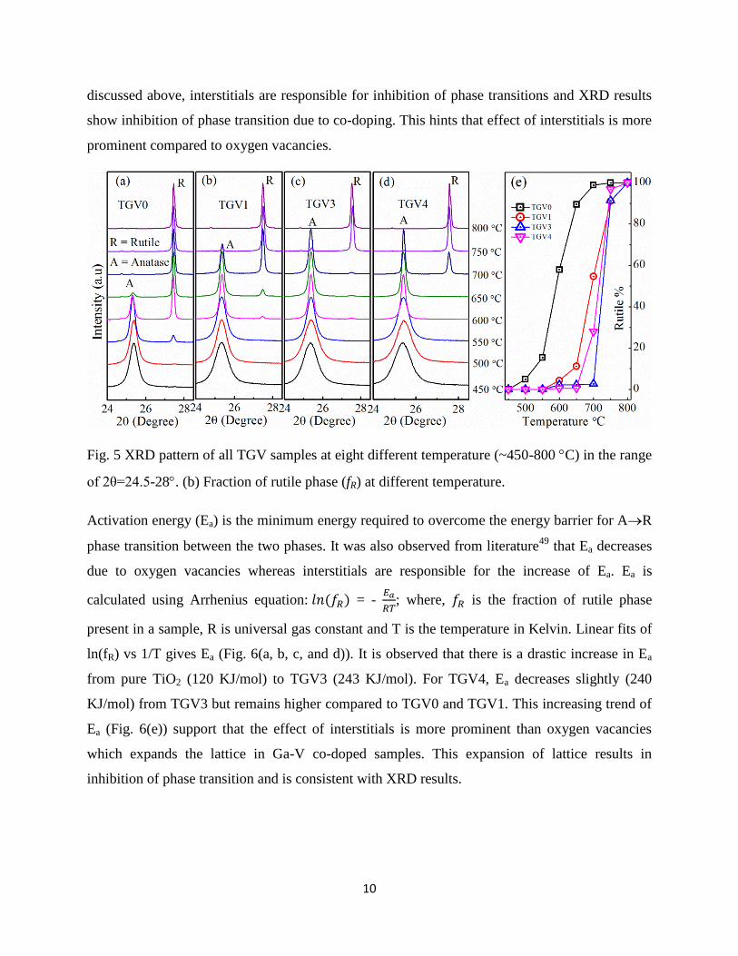
Activation energy (Ea) is the minimum energy required to overcome the energy barrier for AR
phase transition between the two phases. It was also observed from literature49
that Ea decreases
due to oxygen vacancies whereas interstitials are responsible for the increase of Ea. Ea is
calculated using Arrhenius equation: 𝑙𝑛(𝑓𝑅) = - 𝐸𝑎
𝑅𝑇; where, 𝑓𝑅 is the fraction of rutile phase
present in a sample, R is universal gas constant and T is the temperature in Kelvin. Linear fits of
ln(fR) vs 1/T gives Ea (Fig. 6(a, b, c, and d)). It is observed that there is a drastic increase in Ea
from pure TiO2 (120 KJ/mol) to TGV3 (243 KJ/mol). For TGV4, Ea decreases slightly (240
KJ/mol) from TGV3 but remains higher compared to TGV0 and TGV1. This increasing trend of
Ea (Fig. 6(e)) support that the effect of interstitials is more prominent than oxygen vacancies
which expands the lattice in Ga-V co-doped samples. This expansion of lattice results in
inhibition of phase transition and is consistent with XRD results.
11
Fig. 6 Fits of ln(fR) vs 1/T ((a): TGV0; (b): TGV1; (c): TGV3 and (d): TGV4). (b) Variation of
activation energy with doping concentration (solid line is just a guide to the eye).
Samples in anatase phase, when heated to a higher temperature (500 C) leads to rearrangement
of Ti-O bonds as a result unit cell volume contracts and phase transformation (AR) occurs. In
anatase phase, lattice constant ‘a=b’ (3.785 Å) is smaller and ‘c’ (9.514 Å) is larger compared to
lattice constants of rutile phase (a=b=4.59 4Å and c=2.958 Å)14
. Hence, unit cell volume of
anatase phase is larger (136.3 Å3) compared to rutile phase (62.4 Å
3). For phase transition, ‘a’
always increase and ‘c’ decrease. Hence, this delay of phase transition can be explained in terms
of change in lattice constants.
Fig. 7(a) shows the Rietveld refinement of TGV samples in pure anatase phase (450 C). It is
observed that all the three lattice constant increases with increasing doping concentration (Fig.
7(b)). Unit cell volume also follows the similar trend as observed in lattice constants (Fig. 7(c)).
Cr3+
has a comparable ionic radius (0.755 Å) as Ga3+
and has same charge state. Zhu et al.50
from
their DFT calculation showed that anatase phase formation energy is low when Cr3+
occupies
interstitials sites than substitutional sites. With increasing doping concentration, Cr3+
going from
interstitial to substitutional sites was observed to vary. Hence, Ga3+
ions too may have the same
tendency to go more into interstitial sites than substitutional sites. Banerjee et al.51
experimentally showed that Ga3+
ions occupy more interstitial sites than substitutional sites in
TiO2. These interstitial sites are responsible for the expansion of lattice and inhibit the phase
transition. Depero et al.34
experimentally proved that Ga doping inhibits phase transition. It was
also observed that formation energy of anatase TiO2 is low when V occupies the substitutional

12
sites rather than interstitial sites52
. Hence, theoretically and experimentally it was proved that V
occupies substitutional sites in TiO2 35, 53, 54
and thereby decrease all the three lattice constants.
This is because V4+/5+
have smaller ionic radius compared to Ti4+
. Vittadini et al.55
reported that
V5+
is more likely the major surface species where V4+
is stable inside balk. From TEM results it
was observed that particle is in a spherical shape and in nano size. With increasing doping
concentration, particle size decreases which result to increase the surface area to volume ratio of
the samples. BET measurement shows surface area increases with increasing doping
concentration. Hence at anatase phase, all the Vanadium ions are mostly in 5+ oxidation states42,
54. Hence, contraction of lattice constants and thereby unit cell volume by V incorporation
promoted the AR phase transition16
. In all the co-doped samples as Ga content is more
compared to V (Ga:V=4:1), hence the effect of Ga interstitial play a significant role over V
substitution and oxygen vacancies which expands the lattice. Rietveld refinement on anatase
phase shows this expansion of lattice and results in inhibition of phase transition.
Fig. 7(a) Rietveld refinement of anatase TGV samples (450 C). Change of lattice constants (b),
and unit cell volume (c) with Ga-V doping concentration.

13
From Rietveld refinement on rutile phase (800 ⁰C), it is observed that lattice constant ‘a’ and ‘b’
increases with increasing doping concentration. However, lattice constant ‘c’ nominally
increases for TGV1 and thereafter decreases rapidly for TGV3 and TGV4. Unit cell volume also
increases for TGV1 and thereafter decreases (for TGV3 and TGV4). As mentioned above that
for TGV3 and TGV4, due to thermal instability and less space, few Ga ions move out from
lattice structure. Hence, relative percentage of V4+/5+
ions compared to Ga3+
ions increases from
targeted values (4:1). At rutile phase, due to high temperature (800 ⁰C) particle size increases for
all TGV samples and with increasing doping content grain growth process enhanced (discussed
later at Fig. 9). Hence surface area to volume ratio decreases which results to increase in V4+
species in the samples as discussed above that V4+
is more likely stable into bulk. In our earlier
report16
, it was observed that V ions are in mixed valence states of V5+
/V4+
and with increasing
doping concentration presence of V4+
ions increases. In rutile phase, both the V5+
and V4+
ions
occupy the substitutional sites in TiO2 lattice. V5+/4+
ions have smaller ionic radius compared to
Ti4+
and Ga3+
which results in a decrease of lattice constants ‘c’ as well as unit cell volume. Ga3+
ions occupy more interstitials sites than substitutional sites in TiO2 discussed above. At lower
doping (TGV1), as all the Ga ions are inside the crystal structure and due to significant role of
this Ga3+
interstitials unit cell volume increased. However at higher doping (TGV3 and TGV4),
due to substitutional V4+/5+
ions and oxygen vacancies unit cell volume decreased.
Fig. 8 Change in lattice constants (a) and unit cell volume (b) with co-doping concentration at
rutile phase (800 C).

14
To investigate the effect of Ga and V co-doping on grain growth process, crystallite size (at 450
C) is calculated using Scherrer equation. It is observed that crystallite size decreases from 14.5
(pure TiO2) nm to 8.9 nm (TGV4) by Ga-V incorporation (Fig. 9(e)). Hence co-doping restrains
the grain growth process of anatase nanoparticles which is consistent with TEM results. In most
metal oxides this restrains grain growth is due to increasing strain in the nanoparticles.
Such increase of strain in lattice due to Ga-V co-doping has been verified by the shape and peak
positions of pure anatase TGV samples (at 450 C). Usually, crystallites in polycrystalline
aggregates are in a state of compression or tension by its neighboring crystallites which produce
uniform or non-uniform strain in the lattice. From literature, it was observed that shifting of
diffraction peak creates uniform strain whereas peak broadening without changing peak position
creates non-uniform strain 51
. Careful inspection reveals that the 101 peak become broad but
position remain almost same in TGV samples (provided in supplementary file Fig. S2). Hence,
incorporation of Ga3+
/V4+/5+
at lattice site and as well as in interstitial site may be responsible for
such nonuniform stain. Williamson Hall plot is used to calculate quantitative changes in strain
due to Ga-V co-doping. Slop of linear fits of cos() vs 4sin() gives strain; where is the
FWHM of corresponding peaks of XRD spectra. It is observed that strain increases with doping
concentration (Fig. 9(e)). This increasing strain due to Ga-V incorporation retards the grain
growth process of anatase nanoparticle.
Fig. 9 Linear fits of cos(θ) vs 4sin(θ) of TGV samples in anatase phase (450 C). (e) change of
strain and crystallite size with doping concentration.

15
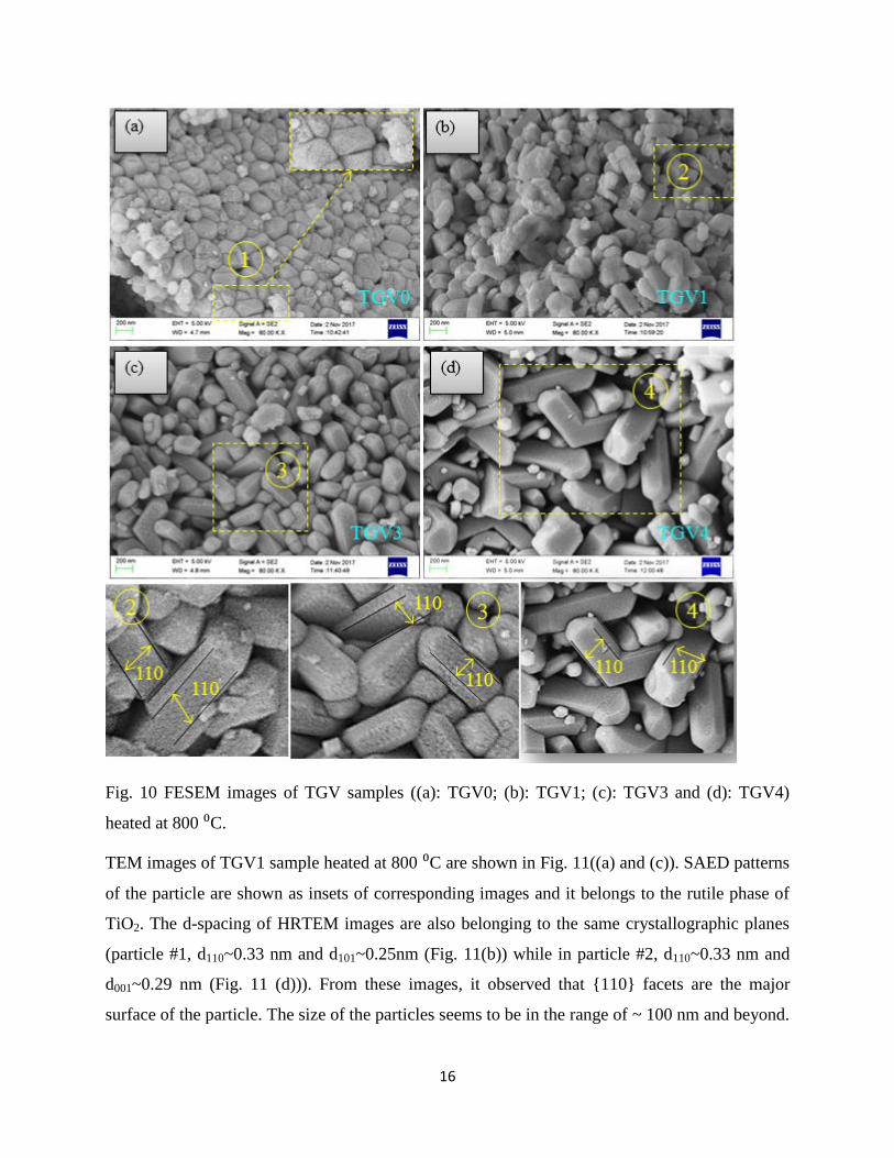
Fig. 10 shows the FESEM images of TGV samples at rutile phase (800 ⁰C). Oliver et al. 56
, from
their DFT calculations on rutile phase, reported that {110} surface has the lowest surface energy
(1.78 J/m2) whereas {100} surface perpendicular to {110} surface has the highest surface energy
(2.08 J/m2). During crystal growth, the low energy surface {110} grows fastest and high energy
surface {100} tend to decrease its surface area to minimize the total energy per crystal57
. As
mentioned above, particles of anatase TGV samples (450 ⁰C) are almost in a spherical shape.
With increasing temperature anatase phase converted into mixed phase and with further heating
transform into an entirely rutile phase. Similarly, particle shape and size also changed with
temperature. With increasing temperature spherical anatase crystals enlarge its size and become
elongate spherical to a rod-like structure. For pure TiO2 (TGV0), particles are in irregular
spherical shape or distorted rod-like structure and average particle size is ~200 nm (calculated
using Image J software). From these images (all the images are in same magnification), it clearly
observed that particles have prominent rod-like structure and grain growth process enhanced
with increasing doping concentration. It was observed that Ga doping restrain the rutile grain
growth process34
. Whereas in earlier reports it was observed that V enhanced the grain growth
process16
. Effect of Vanadium is more sensitive in grain growth process of rutile particle than
Gallium. Hence, the faster grain growth process in co-doped samples is mainly due to the effect
of vanadium. According to the nature of surface edges and area at par with reported literature,
{110} surfaces are the most prominent surfaces of rutile particle56, 58, 59
. Some portions of
FESEM images of TGV samples have been zoomed to show these surfaces. For TGV0 samples,
the zoomed view is shown in the inset of Fig. 10(a). The zoomed views of the co-doped samples
are shown as ② (TGV1), ③ (TGV3), and ④ (TGV4).
16
Fig. 10 FESEM images of TGV samples ((a): TGV0; (b): TGV1; (c): TGV3 and (d): TGV4)
heated at 800 ⁰C.
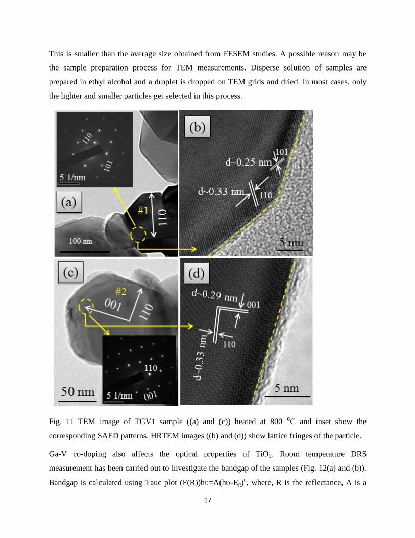
TEM images of TGV1 sample heated at 800 ⁰C are shown in Fig. 11((a) and (c)). SAED patterns
of the particle are shown as insets of corresponding images and it belongs to the rutile phase of
TiO2. The d-spacing of HRTEM images are also belonging to the same crystallographic planes
(particle #1, d110~0.33 nm and d101~0.25nm (Fig. 11(b)) while in particle #2, d110~0.33 nm and
d001~0.29 nm (Fig. 11 (d))). From these images, it observed that {110} facets are the major
surface of the particle. The size of the particles seems to be in the range of ~ 100 nm and beyond.
17
This is smaller than the average size obtained from FESEM studies. A possible reason may be
the sample preparation process for TEM measurements. Disperse solution of samples are
prepared in ethyl alcohol and a droplet is dropped on TEM grids and dried. In most cases, only
the lighter and smaller particles get selected in this process.
Fig. 11 TEM image of TGV1 sample ((a) and (c)) heated at 800 ⁰C and inset show the
corresponding SAED patterns. HRTEM images ((b) and (d)) show lattice fringes of the particle.
Ga-V co-doping also affects the optical properties of TiO2. Room temperature DRS
measurement has been carried out to investigate the bandgap of the samples (Fig. 12(a) and (b)).
Bandgap is calculated using Tauc plot (F(R))hʋ=A(h-Eg)n, where, R is the reflectance, A is a

18
constant, h is the frequency of illumination, Eg is the bandgap and n is a unitless parameter with
value ½ or 2 for direct or indirect bandgap semiconductor respectively. From literature, it was
observed that anatase is an indirect (n=2) bandgap whereas rutile is direct (n=1/2) bandgap
semiconductor17
. It is observed that bandgap decreases due to co-doping for both the phases. At
anatase phase, bandgap decreases from 3.14 eV (TGV0) to 2.86 eV (TGV4) (Fig. 12(c)) and at
rutile phase, bandgap decreases from 3.06 (TGV0) to 2.84 eV (TGV4) (Fig. 12(d)). O 2p and
Ti3d hybridization (p-d) form strong bonding states which are responsible to form valence band
(VB) in TiO2. On the other hand, antibonding states due to p-d hybridization between O 2p, Ti
3d, and Ti 2p form conduction band (CB)17
. Due to Ga doping, the hybridization between O 2p,
Ti 3d, and Ga 3d becomes weaker and form empty states in the bandgap of TiO2 which therefore
widen the conduction band33, 60
. This results in increasing the bandgap. From literature, it was
also observed that effect of Ga for enhancement of bandgap is not much pronounced21, 33, 51, 61
. In
case of V doped TiO2, p-d hybridization of O 2p, Ti 3d, and V 3d form impurity energy levels
(or donor levels) inside the bandgap. Due to these energy levels bandgap decreases42
. It was also
observed that effect of V is more sensitive compared to Ga for bandgap change. Hence, due to
combined effect of both V and Ga, bandgap decreases in co-doped samples.
In case of rutile phase, bandgap gradually shifted to lower values from 3.06 eV (TGV0) to 2.84
eV (TGV4) with increasing doping concentration. For TGV1, bandgap shows slight red shift
because V concentration is very low in the samples (Ga: V ~ 4:1). For TGV3 and TGV4, it is
observed from XRD data that some amount of Ga3+
ions move out of the lattice and forms -
Ga2O3 phase. Hence, relative amount of V4+/5+
to Ga3+
is increased (Ga:V=4:1; ratio decreased)
compared to intended values. It was discussed that V4+
ion is more effective than V5+
ion in
reducing the bandgap62
of TiO2: (Eg(V4+
)Eg(V5+
)). This may also be a reason, for a gradual shift
of bandgap in rutile phase.
Structural modifications are inevitable when foreign elements are incorporated into any lattice. It
is known that electronic band structure is strongly correlated with a lattice structure. Urbach
energy (EU) is a measure of lattice distortion in the samples which affects electronic band
structure 63, 64
. In most semiconductors, it was observed that bandgap decreases if EU increases65,
66. EU is calculated from linear fits of “lnF(R)-hʋ” plots just below the absorption edge of DRS
data. Reciprocal of the slope gives EU54
. In anatase phase, EU decrease from 145 meV for TGV0

19
to 506 meV for TGV4 (Fig. 12(c)). Whereas for rutile phase; EU decrease from 63 meV for
TGV0 to 256 meV for TGV4 (Fig. 12(d)). This increase in EU signifies a more distorted lattice
due to co-doping and a band tailing (Urbach tail) just below absorption edge.
Fig. 12 Room temperature DRS data of co-doped (Ga-V) samples in anatase (a) and rutile phase
(b). Inset shows the change of bandgap with co-doping concentration for corresponding samples.
As mentioned above for pure TiO2, phase transition (AR) starts in between 450-500 ⁰C. Upon
co-doping, anatase phase becomes stable up to ~650 ⁰C. Surface area plays an important role for
PCA. In the anatase phase, nano-sized spherical particles (8-15 nm) provide a large surface area
and BET analysis confirms this increasing trend of surface area with doping concentration. This
provides a larger number of active sites for PCA. V decreases the bandgap to visible regions
while Ga inhibits phase transition, thereby making the materials a promising candidate for “high
temperature visible light photocatalytic application.”

20
Conclusions
Uncompensated Ga-V co-doped TiO2 has been prepared successfully by modified sol-gel
process. Inhibition of phase transition due to co-doping is confirmed by XRD spectra. Activation
energy of phase transition increases from 120 KJ/mol (x=0) to 240 KJ/mol (x=0.046) by Ga-V
incorporation which also reveals this inhibition of phase transition. Ga ions occupy more
interstitial sites than substitutional sites whereas V ions occupy substitutional sites in TiO2. In
anatase phase, lattice constant increases by the effect of Ga3+
interstitials, as Ga content is more
than V content (Ga:V:=4:1). This expansion of lattice results in inhibition of phase transition.
Hence, anatase phase becomes stable up to ~650 C in co-doped sample. In anatase phase, grain
growth process restrained as strain increases by the effect of co-doping and thereby reduces
crystallite size. In rutile phase, grain growth process in co-doped sample is enhanced mainly by
the effect of Vanadium. Bandgap decreases in both phases and reduces to the visible light region.
BET analysis shows that surface area increases from 4.55 m2/g (x=0) to 96.53 m
2/g (x=0.046) by
Ga-V incorporation. Hence, co-doped anatase nanoparticles can be used as a good photocatalyst
using visible light up to a higher temperature ~650 C.
Acknowledgment
The authors are sincerely thanking IIT Indore for providing funds and all research related
facilities. The authors also thank Sophisticated Instrument Centre (SIC) of IIT Indore for TGA,
BET, and FESEM studies. One of the authors (Dr. Sajal Biring) acknowledges support from
Ministry of Science and Technology, Taiwan (MOST 105-2218-E-131-003 and 106-2221-E-
131-027).
References
1. M. Zukalova, A. Zukal, L. Kavan, M. K. Nazeeruddin, P. Liska and M. Gratzel, Nano. Lett. 5 (9),
1789-1792 (2005).
2. B. E. Hardin, E. T. Hoke, P. B. Armstrong, J.-H. Yum, P. Comte, T. Torres, J. M. J. Fréchet, M.
K. Nazeeruddin, M. Grätzel and M. D. McGehee, Nat. Photonics 3 (7), 406-411 (2009).
3. N. Abidi, L. Cabrales and E. Hequet, ACS Appl. Mater. Interfaces 1 (10), 2141-2146 (2009).
4. C. Fan, C. Chen, J. Wang, X. Fu, Z. Ren, G. Qian and Z. Wang, Sci. Rep. 5, 11712 (2015).
5. R. Ren, Z. Wen, S. Cui, Y. Hou, X. Guo and J. Chen, Sci. Rep. 5, 10714 (2015).
6. B. Park and E. J. Cairns, Electrochem. Comm. 13 (1), 75-77 (2011).
7. T. K. Das, P. Ilaiyaraja, P. S. V. Mocherla, G. M. Bhalerao and C. Sudakar, Sol. Energy Mater.
Sol. Cells 144, 194-209 (2016).
8. J.-Y. Liao, J.-W. He, H. Xu, D.-B. Kuang and C.-Y. Su, J. Mater. Chem. 22 (16), 7910 (2012).

21
9. M. J. A. Ruszala, N. A. Rowson, L. M. Grover and R. A. Choudhery, Int. J. Chem. Eng. Appl. 6
(5), 331-340 (2015).
10. Y. Wang, J. Li, L. Wang, T. Qi, D. Chen and W. Wang, Chem. Eng.Technol. 34 (6), 905-913
(2011).
11. T. Kamegawa, J. Sonoda, K. Sugimura, K. Mori and H. Yamashita, J. Alloys. Compound. 486 (1-
2), 685-688 (2009).
12. V. N. Koparde and P. T. Cummings, ACS Nano 2 (8), 1620-1624 (2008).
13. J. Muscat, V. Swamy and N. M. Harrison, Phys. Rev. B 65 (22) (2002).
14. D. A. H. Hanaor and C. C. Sorrell, J. Mater. Sci. 46 (4), 855-874 (2010).
15. K. Ding, Z. Miao, B. Hu, G. An, Z. Sun, B. Han and Z. Liu, Langmuir 26 (12), 10294-10302
(2010).
16. N. Khatun, Anita, P. Rajput, D. Bhattacharya, S. N. Jha, S. Biring and S. Sen, Ceram. Int. 43
(16), 14128-14134 (2017).
17. J. Zhang, P. Zhou, J. Liu and J. Yu, Phys. Chem. Chem. Phys. 16 (38), 20382-20386 (2014).
18. N. Satoh, T. Nakashima and K. Yamamoto, Sci. Rep. 3, 1959 (2013).
19. Q. L. XiaoBo Li, XiaoYing Jiang, Jianhua Huang, Int. J. Electrochem. Sci. 7, 11519-11527
(2012).
20. A. Sclafani and J. M. Herrmann, J. Phys. Chem. 100 (32), 13655-13661 (1996).
21. A. K. Chandiran, F. d. r. Sauvage, L. Etgar and M. Graetzel, J. Phys. Chem. C 115 (18), 9232-
9240 (2011).
22. B. Buchholcz, H. Haspel, Á. Kukovecz and Z. Kónya, CrystEngComm 16 (32), 7486 (2014).
23. C. Huang, X. Liu, L. Kong, W. Lan, Q. Su and Y. Wang, Appl. Phys. A 87 (4), 781-786 (2007).
24. A. Zaleska, Recent Patents on Engineering 2 (3), 157-164 (2008).
25. C. Rath, P. Mohanty, A. C. Pandey and N. C. Mishra, J. Phys. D: Appl. Phys. 42 (20), 205101
(2009).
26. G. Rajender and P. K. Giri, J. Alloys. Compound. 676, 591-600 (2016).
27. Anita, A. K. Yadav, N. Khatun, S. Kumar, C.-M. Tseng, S. Biring and S. Sen, J. Mater. Sci.:
Mater. Electron. (2017).
28. W. Choi, A. Termin and M. R. Hoffmann, J. Phys. Chem. 98 (51), 13669-13679 (1994).
29. B. Choudhury, A. Choudhury and D. Borah, J. Alloys. Compound. 646, 692-698 (2015).
30. Y. Zhang, Y. Shen, F. Gu, M. Wu, Y. Xie and J. Zhang, Appl. Surf. Sci. 256 (1), 85-89 (2009).
31. N. Khatun, R. Amin, Anita and S. Sen, AIP Conf. Proc. 1953, 040028 (2018).
32. G. Hassnain Jaffari, A. Tahir, N. Z. Ali, A. Ali and U. S. Qurashi, J. Appl. Phys. 123 (16),
161541 (2018).
33. S. Luo, T. D. Nguyen-Phan, D. Vovchok, I. Waluyo, R. M. Palomino, A. D. Gamalski, L. Barrio,
W. Xu, D. E. Polyansky, J. A. Rodriguez and S. D. Senanayake, Phys. Chem. Chem. Phys. 20 (3), 2104-
2112 (2018).
34. L. E. Depero, A. Marino, B. Allieri, E. Bontempi, L. Sangaletti, C. Casale and M. Notaro, J.
Mater. Res. 15 (10), 2080-2086 (2011).
35. W. Avansi, R. Arenal, V. R. de Mendonça, C. Ribeiro and E. Longo, CrystEngComm 16 (23),
5021 (2014).
36. S. Klosek and D. Raftery, J. Phys. Chem. B 105 (14), 2815-2819 (2001).
37. S. Shang, X. Jiao and D. Chen, ACS Appl. Mater. Interfaces 4 (2), 860-865 (2012).
38. X. Jiang, T. Herricks and Y. Xia, Adv. Mater. 15 (14), 1205-1209 (2003).
39. H. Yaghoubi, N. Taghavinia, E. K. Alamdari and A. A. Volinsky, ACS Appl. Mater. Interfaces 2
(9), 2629-2636 (2010).
40. M. V. Swapna and K. R. Haridas, J. Exp. Nanosci. 11 (7), 540-549 (2015).
41. V. Caratto, L. Setti, S. Campodonico, M. M. Carnasciali, R. Botter and M. Ferretti, J. Sol-Gel
Sci. Technol. 63 (1), 16-22 (2012).
42. W. Zhou, Q. Liu, Z. Zhu and J. Zhang, J. Phys. D: Appl. Phys. 43 (3), 035301 (2010).
22
43. K. Farhadian Azizi and M. M. Bagheri-Mohagheghi, J. Sol-Gel Sci. Technol. 65 (3), 329-335
(2012).
44. A. B.-N. A. Shalaby, R. Iordanova, Y. Dimitriev, J. Chem. Technol. Metall. 48, 585-590 (2013).
45. M. Thommes, K. Kaneko, A. V. Neimark, J. P. Olivier, F. Rodriguez-Reinoso, J. Rouquerol and
K. S. W. Sing, Pure Appl. Chem. 87 (9-10) (2015).
46. W.-J. Yin, S. Chen, J.-H. Yang, X.-G. Gong, Y. Yan and S.-H. Wei, Appl. Phys. Lett. 96 (22),
221901 (2010).
47. R. A. Spurr and H. Myers, Anal.l Chem. 29 (5), 760-762 (1957).
48. R. D. Shannon and J. A. Pask, J. Am. Ceram. Soc. 48 (8), 391-398 (1965).
49. M. A. Malati and W. K. Wong, Surf. Technol. 22 (4), 305-322 (1984).
50. W. Zhu, X. Qiu, V. Iancu, X. Q. Chen, H. Pan, W. Wang, N. M. Dimitrijevic, T. Rajh, H. M.
Meyer, 3rd, M. P. Paranthaman, G. M. Stocks, H. H. Weitering, B. Gu, G. Eres and Z. Zhang, Phys. Rev.
Lett. 103 (22), 226401 (2009).
51. A. N. Banerjee, S. W. Joo and B.-K. Min, J. Nanomater. 2012, 1-14 (2012).
52. R. Long and N. J. English, Chem. Phys. Chem. 11 (12), 2606-2611 (2010).
53. M. Amini, H. Naslhajian and S. M. F. Farnia, New J. Chem. 38 (4), 1581 (2014).
54. N. Khatun, E. G. Rini, P. Shirage, P. Rajput, S. N. Jha and S. Sen, Mater. Sci. Semicon. Proc. 50,
7-13 (2016).
55. A. Vittadini, M. Casarin and A. Selloni, J Phys Chem B 109 (5), 1652-1655 (2005).
56. P. M. Oliver, G. W. Watson, E. T. Kelsey and S. C. Parker, J. Mater. Chem. 7 (3), 563-568
(1997).
57. A. S. Barnard and P. Zapol, Phys. Rev. B 70 (23) (2004).
58. Z. Lai, F. Peng, H. Wang, H. Yu, S. Zhang and H. Zhao, J. Mater. Chem. A 1 (13), 4182 (2013).
59. T. Ohno, K. Sarukawa and M. Matsumura, New J. Chem. 26 (9), 1167-1170 (2002).
60. C. Gionco, S. Livraghi, S. Maurelli, E. Giamello, S. Tosoni, C. Di Valentin and G. Pacchioni,
Chem. Mater. 27 (11), 3936-3945 (2015).
61. S. Sudou, K. Kado and K. Nakamura, Trans. Mater. Res. Soc. Japan 35 (1), 171-174 (2010).
62. A. Y. Choi and C.-H. Han, J. Nanosci.Nanotechnol. 14 (10), 8070-8073 (2014).
63. S. J. Ikhmayies and R. N. Ahmad-Bitar, J. Mater. Res.Technol. 2 (3), 221-227 (2013).
64. A. Paleari, F. Meinardi, A. Lauria, R. Lorenzi, N. Chiodini and S. Brovelli, Appl. Phys. Lett. 91
(14), 141913 (2007).
65. A. S. Hassanien and A. A. Akl, J. Alloys. Compound. 648, 280-290 (2015).
66. S. Benramache, B. Benhaoua and F. Chabane, J. Semicon. 33 (9), 093001 (2012).