paper design of “bubble-inspired single-electron circuit
TRANSCRIPT

NOLTA, IEICE
Paper
Design of“bubble-inspired single-electron circuit”mimicking behavior of bubble film
Nobuhiko Kurata 1a) and Takahide Oya 1
1 Graduate School of Engineering Science, Yokohama National University
Tokiwadai 79-5, Hodogaya-ku, Yokohama 240-8501, Japan
Received January 9, 2019; Revised May 17, 2019; Published October 1, 2019
Abstract: We propose a novel single-electron (SE) circuit with unique information-processingthat mimics the behavior of bubble film, i.e., a “bubble-inspired SE circuit.” It is knownthat the behavior of bubble film can be assumed to solve the shortest Steiner problem. In thisstudy, we focus on the behavior to design a novel SE circuit. For this, there are three importantpoints, we believe, for mimicking the behavior for the circuit: 1) the film gradually shrinking,2) the film stopping shrinking when reaching points like pillars, and 3) films stopping shrinkingwhen they collide with each other. We here designed and tested our SE circuit. By computersimulation, we confirmed that the designed circuit displayed the three processes correctly asdesired. Therefore, the “bubble-inspired SE circuit” we designed has the potential for novelinformation processing.
Key Words: single-electron circuit, bubble film, natural phenomenon, Steiner problem
1. IntroductionIn recent years, the necessity of processing vast amounts of information has increased because ofadvances in today’s information society. For this, technology for miniaturizing CMOS LSI devices hasadvanced, improving their information processing performance. In addition, due to this technologicalinnovation (advances in nanotechnology), nano-scale devices (e.g., single-electron devices [1]) havegained focus due to their unique properties, and the design, construction, and fabrication of their unitelements is more possible than ever before. In this study, we focus on single-electron (SE) devices asthe targeted devices. Generally, SE devices that can operate using individual electrons by controllinga quantum effect (Coulomb blockade) have tunneling junctions as a main component [2]. It is knownthat this has many advantages, including extremely low power consumption and high integrability [3].However, there is a problem in that no optimal way for information-processing has been established,although many applications for SE devices have been proposed up to now [4–6]. As a candidate, wedraw inspiration from a natural phenomenon, i.e., behaviors shown in soap bubble films, that canbe regarded as a form of information processing [7]. Bubble film forms a special structure caused bythe surface tension of the film having minimum energy. From the perspective of engineering, it can
399
Nonlinear Theory and Its Applications, IEICE, vol. 10, no. 4, pp. 399–413 c©IEICE 2019 DOI: 10.1587/nolta.10.399
be assumed that a certain nonlinear problem, that is, the shortest Steiner problem, can be solvedby using this property. For example, when two plastic boards are prepared, placed face to face,connected to each other by using a few plastic pillars, immersed in a bubble liquid, and pulled up, thebubble film shrinks depending on where the pillars were placed. It is known that the shrunken formof this film shows the solution to the shortest Steiner problem [8]. In this study, we aim to design anovel information-processing system with SE devices that can solve the shortest Steiner problem bymimicking the behavior of bubble film.
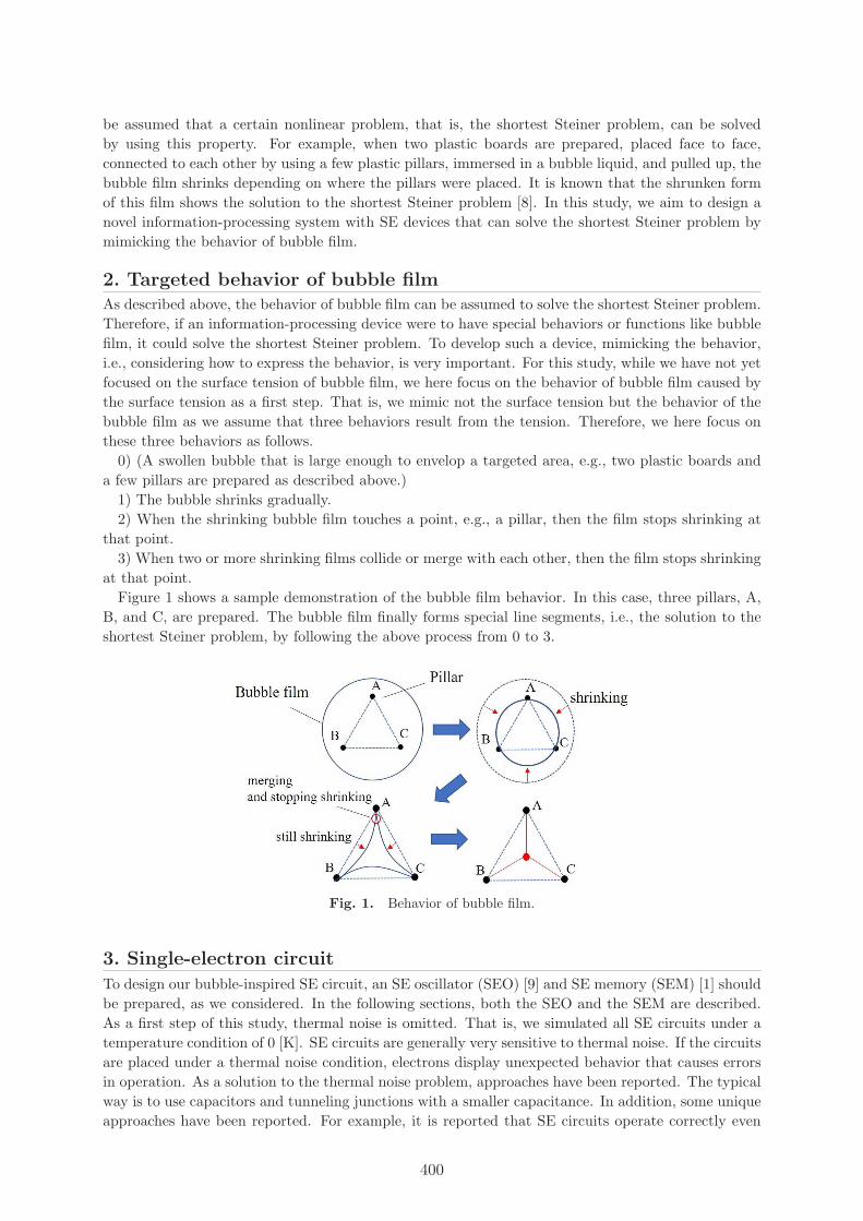
2. Targeted behavior of bubble filmAs described above, the behavior of bubble film can be assumed to solve the shortest Steiner problem.Therefore, if an information-processing device were to have special behaviors or functions like bubblefilm, it could solve the shortest Steiner problem. To develop such a device, mimicking the behavior,i.e., considering how to express the behavior, is very important. For this study, while we have not yetfocused on the surface tension of bubble film, we here focus on the behavior of bubble film caused bythe surface tension as a first step. That is, we mimic not the surface tension but the behavior of thebubble film as we assume that three behaviors result from the tension. Therefore, we here focus onthese three behaviors as follows.
0) (A swollen bubble that is large enough to envelop a targeted area, e.g., two plastic boards anda few pillars are prepared as described above.)
1) The bubble shrinks gradually.2) When the shrinking bubble film touches a point, e.g., a pillar, then the film stops shrinking at
that point.3) When two or more shrinking films collide or merge with each other, then the film stops shrinking
at that point.Figure 1 shows a sample demonstration of the bubble film behavior. In this case, three pillars, A,
B, and C, are prepared. The bubble film finally forms special line segments, i.e., the solution to theshortest Steiner problem, by following the above process from 0 to 3.
Fig. 1. Behavior of bubble film.
3. Single-electron circuit
To design our bubble-inspired SE circuit, an SE oscillator (SEO) [9] and SE memory (SEM) [1] shouldbe prepared, as we considered. In the following sections, both the SEO and the SEM are described.As a first step of this study, thermal noise is omitted. That is, we simulated all SE circuits under atemperature condition of 0 [K]. SE circuits are generally very sensitive to thermal noise. If the circuitsare placed under a thermal noise condition, electrons display unexpected behavior that causes errorsin operation. As a solution to the thermal noise problem, approaches have been reported. The typicalway is to use capacitors and tunneling junctions with a smaller capacitance. In addition, some uniqueapproaches have been reported. For example, it is reported that SE circuits operate correctly even
400

under the thermal noise condition when the circuits are constructed to mimic stochastic resonance(SR) behavior in neural networks (e.g., [10]). A system with SR behavior can be considered as acertain type of noise-energy-harnessing system, and it will operate correctly under the thermal noisecondition. We expect our circuit to operate correctly under the condition when the above ways areapplied in the near future. However, we here omitted thermal noise for simplicity.
3.1 Single-electron oscillatorThe SEO consists of a bias voltage source Vd, a high resistance R, and a tunneling junction Cj inseries. Figure 2 shows a schematic of the SEO. Because of the contained tunneling junction, theSEO operates as a threshold element. That is, the tunneling junction has a threshold voltage forelectrons to tunnel through it. When a Vd that is set to higher than the threshold value is applied tothe SEO, the electron tunneling probabilistically occurs. Then, the node voltage Vn changes sharply.An example of the operation of the SEO is shown in Fig. 3. In this case, the Vd was set to the sub-
Fig. 2. Single-electron oscillator.
Fig. 3. Example operation of single-electron oscillator (Vd = 7 mV , R =1 GΩ, Cj = 10 aF).
Fig. 4. One-dimensional arrayed single-electron oscillator system.
401

Fig. 5. Example operation of system (Fig. 4) (Vd = 5.7 mV, R = 200 MΩ,Cj = 10 aF, C = 2 aF).
Fig. 6. Two-dimensional arrayed single-electron oscillator system.
threshold value of the SEO. When an external trigger voltage was inputted, then Vn exceeded thethreshold voltage. After that, electron tunneling occurred, and the Vn changed sharply. From this,it is possible to control the electron tunneling by inputting a trigger or not. Moreover, the voltagechange can be propagated by connecting SEOs because changing Vn in an SEO can be a triggerinput for the adjacent ones. For example, when SEOs are arrayed and connected one-dimensionallyas shown in Fig. 4, the voltage change can propagate in the circuit because of continuous electrontunneling. The result of simulating the circuit in Fig. 4 is shown in Fig. 5. In addition, when the SEOsare arrayed and connected two-dimensionally as shown in Fig. 6, the voltage change can propagate
402
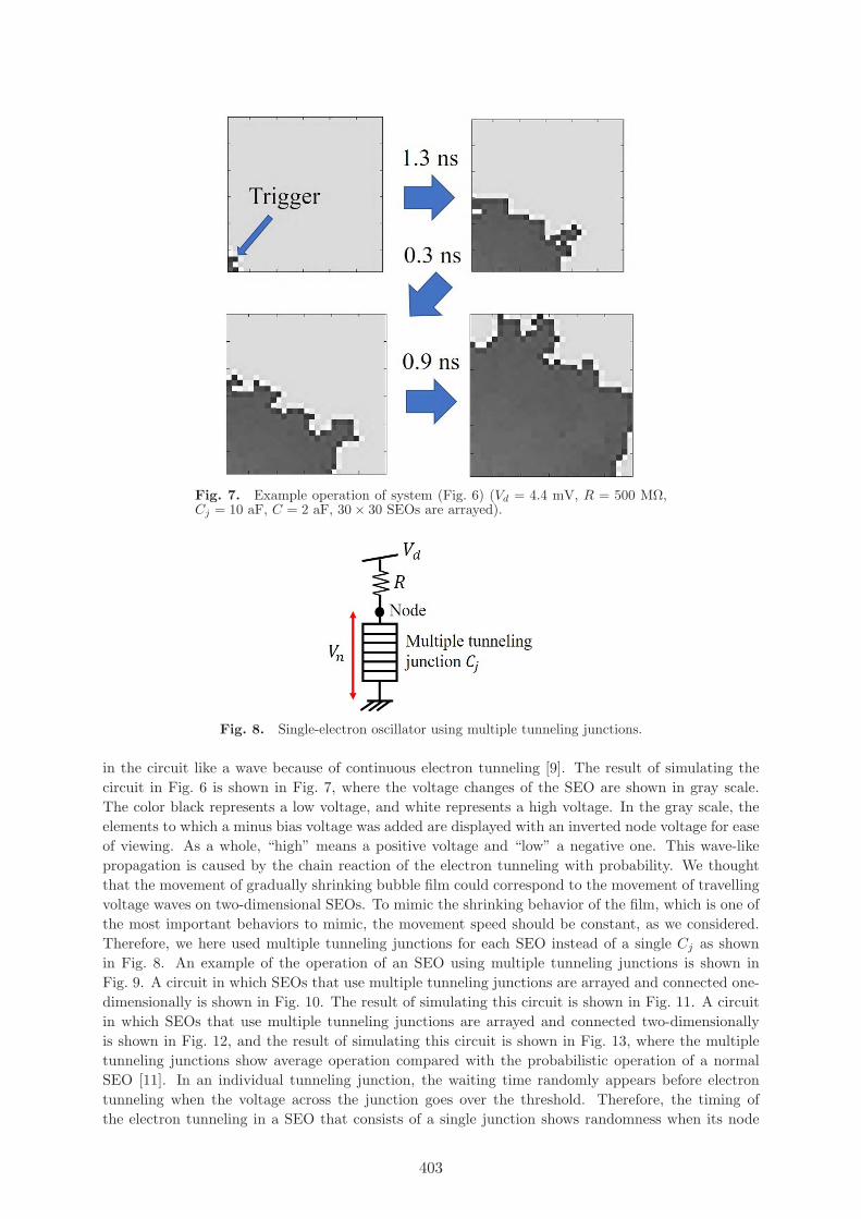
Fig. 7. Example operation of system (Fig. 6) (Vd = 4.4 mV, R = 500 MΩ,Cj = 10 aF, C = 2 aF, 30 × 30 SEOs are arrayed).
Fig. 8. Single-electron oscillator using multiple tunneling junctions.
in the circuit like a wave because of continuous electron tunneling [9]. The result of simulating thecircuit in Fig. 6 is shown in Fig. 7, where the voltage changes of the SEO are shown in gray scale.The color black represents a low voltage, and white represents a high voltage. In the gray scale, theelements to which a minus bias voltage was added are displayed with an inverted node voltage for easeof viewing. As a whole, “high” means a positive voltage and “low” a negative one. This wave-likepropagation is caused by the chain reaction of the electron tunneling with probability. We thoughtthat the movement of gradually shrinking bubble film could correspond to the movement of travellingvoltage waves on two-dimensional SEOs. To mimic the shrinking behavior of the film, which is one ofthe most important behaviors to mimic, the movement speed should be constant, as we considered.Therefore, we here used multiple tunneling junctions for each SEO instead of a single Cj as shownin Fig. 8. An example of the operation of an SEO using multiple tunneling junctions is shown inFig. 9. A circuit in which SEOs that use multiple tunneling junctions are arrayed and connected one-dimensionally is shown in Fig. 10. The result of simulating this circuit is shown in Fig. 11. A circuitin which SEOs that use multiple tunneling junctions are arrayed and connected two-dimensionallyis shown in Fig. 12, and the result of simulating this circuit is shown in Fig. 13, where the multipletunneling junctions show average operation compared with the probabilistic operation of a normalSEO [11]. In an individual tunneling junction, the waiting time randomly appears before electrontunneling when the voltage across the junction goes over the threshold. Therefore, the timing ofthe electron tunneling in a SEO that consists of a single junction shows randomness when its node
403
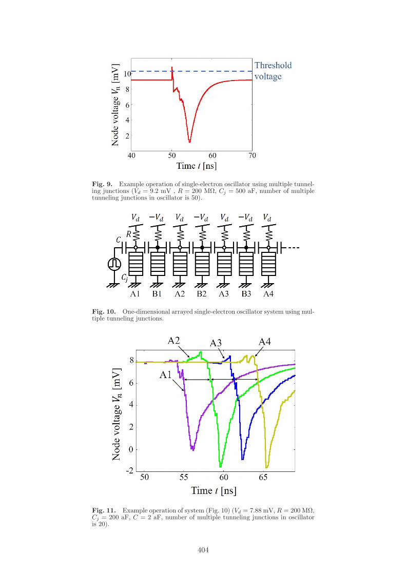
Fig. 9. Example operation of single-electron oscillator using multiple tunnel-ing junctions (Vd = 9.2 mV , R = 200 MΩ, Cj = 500 aF, number of multipletunneling junctions in oscillator is 50).
Fig. 10. One-dimensional arrayed single-electron oscillator system using mul-tiple tunneling junctions.
Fig. 11. Example operation of system (Fig. 10) (Vd = 7.88 mV, R = 200 MΩ,Cj = 200 aF, C = 2 aF, number of multiple tunneling junctions in oscillatoris 20).
404

Fig. 12. Two-dimensional arrayed single-electron oscillator system usingmultiple tunneling junctions.
Fig. 13. Example operation of system (Fig. 12) (Vd = 7.5 mV, R = 200 MΩ,Cj = 100 aF, C = 2 aF, number of multiple tunneling junctions in oscillatoris 10, 30 × 30 SEOs are arrayed).
voltage goes over the threshold, and this randomness causes the random movement speed of the wave-like propagation as shown in Fig. 5. In contrast, if multiple tunneling junctions are used for the SEOinstead of a single junction (Fig. 8), the waiting times are averaged as a whole. That is, if the multipletunneling junctions contain N junctions, the capacitance of the individual junctions is set to Cj/N
compared with the original one. Here, the first electron tunneling occurs in the one N junction thatshows the shortest waiting time among all when the node voltage of the multiple-tunneling-junctionSEO goes over the threshold. After that, the second electron tunneling occurs in the next junction,among the (N − 1) junctions, that shows the shortest waiting time after the first one. For adjacentSEOs in an arrayed SEO network, the sum of the voltage change caused by the electron tunneling in
405

some of the junctions, e.g., about 5 junctions if N is 20, becomes the trigger. Electron tunneling inall of the multiple tunneling junctions is not required for the trigger. The time span caused by theelectron tunneling for the trigger shows almost the same (averaged) value. As a result, the movementof the wave-like propagation in the arrayed SEO network had an average speed as shown in Fig. 11.Therefore, a system consisting of SEOs using multiple tunneling junctions can generate smooth waveshaving a constant propagation speed. The difference in the colors between Figs. 7 and 13 is causedby changes in the node voltage (charging of each tunneling junction after the electron tunneling) ofeach SEO depending on the RC time constant. However, this difference does not influence the circuitoperation. The important point is only the movement of the wave front.
3.2 Single-electron memoryThe SEM consists of a bias voltage source Vd, a capacitor CL, and two tunneling junctions Cjs. Aschematic of the SEM is shown in Fig. 14. The SEM operates as a threshold element with a hysteresischaracteristic as a function of the bias voltage Vd as shown in Fig. 15. Therefore, it is possible to holdtwo states of voltage as a memory element. Aiming for the bubble-inspired circuit, we considered thatSEOs and the SEMs must be connected, i.e., we used the SEOs to mimic the shrinking behavior of
Fig. 14. Single-electron memory.
Fig. 15. Example operation of SEM (CL = 4 aF, Cj = 40 aF).
406

the bubble and the SEMs for output. An example circuit that has an SEO and SEM connected byusing a coupling capacitor C is shown in Fig. 16. Figure 17 shows example operation of the SEO andSEM connected circuit. The fine line represents the operation of the SEO. The heavy line representsthat of the SEM. The bias voltage for the SEM was set to the sub-threshold value on the negativeside as indicated by the black line in Fig. 15. In this case, when the electron tunneling occurs in theSEO, the sudden voltage change of the SEO induces the electrons to tunnel in the SEM as a trigger.Then, the electron tunneling that occurred in the SEO is memorized by the connected SEM.
Fig. 16. Example construction of connecting SEO with SEM.
Fig. 17. Example operation of demonstrated circuit shown in Fig. 16 (Vd1 =5 mV, −Vd2 = −20 mV, R = 1 GΩ, Cj1 = 10 aF, Cj2 = 40 aF, CL = 4 aF,C = 2 aF).
407

4. Design of bubble-inspired single-electron circuit
If the processes (behaviors 1 to 3) as described in Sec. 2 can be mimicked on an electronic device,the device must operate as a “bubble-inspired device.” We here express the bubble film behavior onan SE circuit through a combination of SEO and SEM. To design our bubble-inspired SE circuit, weexpress the shrinking behavior of the bubble by using a two-dimensional array of SEOs. We consideredthat processes 0 to 3 as described in Sec. 2 can be expressed by the arrayed SEOs. This is becausethe traveling voltage wave can correspond to the behavior of shrinking bubble film. Therefore, bysetting the trigger on the circle, the changes in voltage gradually propagate to the inside. However,the original arrayed SEOs cannot hold the information of the collision points of waves [9]. Therefore,we here use the SEO and SEM connected circuit as described above. The configuration of the deviceproposed here has three layers for operation, as shown in Fig. 18. In the first layer, a two-dimensionalarray of SEOs using multiple-tunneling-junctions is used. The second and third layers are for sensingcollision points and for output with SEMs. The second layer senses the collision points of the waveson the first layer. For this, each SEM in the second layer is given a bias voltage of −Vd1 and placed
Fig. 18. Bubble-inspired circuit. (a) Schematic of layers and (b) ways ofconnecting elements.
408

just under (same coordinate) the SEOs of the first layer. The SEMs also connect to eight SEOs thatare neighbors of the upper SEOs for the SEMs in the first layer. That is, the SEMs receive eight inputsignals from eight SEOs. The third layer memorizes the information of the collision points. Here, eachSEM in the third layer is given a bias voltage of −Vd2 and connects to SEO #9 in the first layer (theupper SEO of the SEM) and the SEM in the second layer (the SEM under the SEO), i.e., the samecoordinates as the SEO and the SEM. That is, the SEM receives signals that are inputted from SEO#9 in the first layer and the SEM in the second layer. With these, the collision points (merged bubblefilms) are displayed on the third layer, which will be the solution to the shortest Steiner problem.Here, for the first layer, 15 × 15 +Vd-biased SEOs and 15 × 15 −Vd-biased SEOs were prepared, andthey were placed alternately like a checkerboard. For the second layer, −Vd1-biased SEMs and 15×15+Vd1-biased SEMs were prepared. For the third layer, the same as the second layer, −Vd2-biasedSEMs and 15× 15 +Vd2-biased SEMs were prepared. The minus-biased SEMs were connected to theplus-biased SEOs in the first layer, and the plus-biased SEMs were connected to the minus-biasedSEOs in the first layer for operation, as shown in Fig. 18. For operation, we set an appropriatethreshold value for the SEMs of the second and third layers. Concretely, the SEMs are used as thethreshold element. For the second layer, the threshold value is set to 4.5 for the eight inputs. This isbecause the travelling wave front in the first layer has no more than four SEOs in which the electrontunneling occurs. The SEMs will receive more than five inputs, when more than two waves exist justbefore collision in the first layer as shown in Fig. 19. With this, our circuit can detect the collisionpoints of waves on the first layer. For the third layer, the threshold is set to 1.5 for two inputs. As aresult, the voltage change of the second layer propagates slightly later than the wave of the voltagechange of the first layer. When waves collide (merge) in the first layer, electron tunneling occurs atthe same-coordinate SEM of the second layer. In this situation, electron tunneling in the third layerdoes not occur. On wave collision parts, electron tunneling in the SEMs of the second layer occurs inadvance before electron tunneling in the SEOs in the first layer. Therefore, electron tunneling doesnot occur in the SEMs of the third layer. As a result, a difference appears in the node voltage between
Fig. 19. Bubble-inspired single-electron circuit operation.
409

the overlapping parts and the other parts. That is, the third layer corresponds to the result of thecircuit to mimic the behavior of the bubble film.
In this circuit, we used an SEM using four multiple tunneling junctions in the third layer. In ourdesigned circuit, the SEMs in the second layer were placed at the same coordinates as one of theSEOs in first layer, i.e., SEO #9 as shown in Fig. 18. The SEM and SEO #9 must receive inputsignals from neighboring SEOs #1 to #8 in the first layer at the same time. Also, the SEMs in the
Fig. 20. (a) Node voltage change in 1st layer. (b) Node voltage change in 2ndlayer. (c) Node voltage change in 3rd layer [Vd = 7.9 mV, −Vd1 = −27.3 mV,−Vd2 = −25.7 mV, R = 20 GΩ, C = 2.2 aF, Cj = 500 aF, number of multipletunneling junctions in oscillator is 50, 30×30 elements (SEOs for 1st and SEMsfor 2nd and 3rd layers) are arrayed].
410
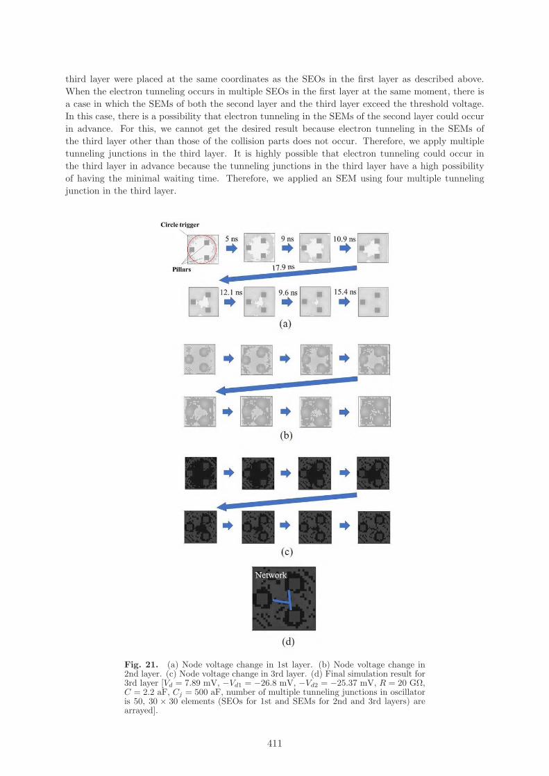
third layer were placed at the same coordinates as the SEOs in the first layer as described above.When the electron tunneling occurs in multiple SEOs in the first layer at the same moment, there isa case in which the SEMs of both the second layer and the third layer exceed the threshold voltage.In this case, there is a possibility that electron tunneling in the SEMs of the second layer could occurin advance. For this, we cannot get the desired result because electron tunneling in the SEMs ofthe third layer other than those of the collision parts does not occur. Therefore, we apply multipletunneling junctions in the third layer. It is highly possible that electron tunneling could occur inthe third layer in advance because the tunneling junctions in the third layer have a high possibilityof having the minimal waiting time. Therefore, we applied an SEM using four multiple tunnelingjunction in the third layer.
Fig. 21. (a) Node voltage change in 1st layer. (b) Node voltage change in2nd layer. (c) Node voltage change in 3rd layer. (d) Final simulation result for3rd layer [Vd = 7.89 mV, −Vd1 = −26.8 mV, −Vd2 = −25.37 mV, R = 20 GΩ,C = 2.2 aF, Cj = 500 aF, number of multiple tunneling junctions in oscillatoris 50, 30 × 30 elements (SEOs for 1st and SEMs for 2nd and 3rd layers) arearrayed].
411

To confirm our circuit operation, we tested it by Monte Carlo simulation. As a first test, we addedtwo triggers on only the lower left and upper right of the first layer. Figure 20 shows the simulationresult. The node voltage Vn is expressed in gray scale. The color white represents high voltage, andblack represents low voltage. In the gray scale, the elements to which a minus bias voltage was addedare displayed with an inverted node voltage for ease of viewing. As a whole, “high” means a positivevoltage, and “low” means a negative one as same as explained in Sec. 3.
In Fig. 20, when the triggers were added on the lower left and upper right in the first layer, thevoltage waves propagated gradually in the first layer. In the second layer, it could be confirmedthat the propagation of the waves was delayed compared with the first layer, but electron tunnelingoccurred in advance on only the collision parts. In the SEMs of the third layer except for the wave-collision parts, electron tunneling occurred immediately after electron tunneling in the SEOs of thefirst layer occurred. In the SEMs of the wave collision parts of the third layer, electron tunneling didnot occur even if electron tunneling in the connected SEOs of the first layer occurred since electrontunneling in the connected SEMs of the second layer occurred in advance. That is, electron tunnelingin the SEMs of the third layer did not occur for only the wave collision parts. Therefore, the “bubble-inspired SE circuit” we designed was confirmed to be as desired. As the second test, triggers on thecircle parts were added in the first layer. Figure 21 shows the simulation result. Here, the pillarswere expressed by turning off the bias voltage in the SEOs in the first layer. That is, the pillars didnot respond even if electron tunneling in the neighboring SEOs occurred. Therefore, when the wavereached the pillars, it spread and propagated, bypassing the pillars. The waves that spread met afterpassing the pillars, i.e., they collided with each other. Then, the second and the third layers detectedthe collision points. As a result, a network of line segments was created.
In Fig. 21, we confirmed that the final display in the third layer formed a network through all pillars.The obtained network shown in Fig. 21 was not the perfect shortest network so far. However, thetotal distance among the three pillars was estimated to differ 12% compared with ideal solution [12].This was not that bad of a result, we thought. Focusing on the first layer, the wave propagation of thefirst layer did not shrink gradually because the pillars where the bias voltage was turned off were set.By setting the pillars, the node voltage in the connected SEOs changed. The changing of the nodevoltage caused fluctuations in the connected SEMs in the second and the third layer. This fluctuationwas propagated throughout the whole circuit, so the wave did not shrink gradually. Therefore, wethink that setting pillars another way and controlling parameters are necessary to improve. If theseproblems are solved, it would be possible to shrink the wave on the circle gradually. In addition, webelieve that it would be possible to obtain networks with other pillar patterns in the near future. Forthis, we are designing additional and modified circuits. In this study, we have found the possibilityof creating a novel device to seek the shortest network through all pillars, although there are someproblems that should be overcome.
5. Conclusion
In this study, we aimed to design a unique SE circuit that mimicked the behavior of bubble film.It is known that the behavior of bubble film can be considered to be a certain type of informationprocessing that solves nonlinear problems. Therefore, we considered that mimicking the behavior onan SE circuit would lead to a novel, functional information-processing device that has the ability tosolve nonlinear problems. By relating the behavior of bubble film with the behavior of the SE circuit,we designed our bubble-inspired circuit. From a first simulation of our designed bubble-inspiredsingle-electron circuit, we confirmed that wave collision parts appeared as we desired. From a secondsimulation, we confirmed that the network appeared through all of the pillars, but many errors wereoutput by causing fluctuations throughout the whole circuit due to the setting of the pillars. Althoughsome problems still remain, we confirmed that our “bubble-inspired single-electron circuit” displayedits own information processing, and it is expected to be a candidate for the next-generation of novelinformation-processing circuits.
412

AcknowledgmentsThis work was partly supported by JSPS KAKENHI Grant Numbers JP16K14242, JP18H03766, andJP19H02545.
References[1] H. Grabert and M.H. Devoret, Single Charge Tunneling: Coulomb Blockade Phenomena in
Nanostructures, Plenum, New York, 1992.[2] K.K. Likharev, “Single-electron devices and their applications,” Institute of Electrical and Elec-
tronics Engineers, vol. 87, pp. 606–632, 1999.[3] D.V. Averin and K.K. Likharev, “Coulomb blockade of single-electron tunneling, and coherent
oscillations in small tunnel junctions,” Journal of Low Temperature Physics, vol. 62, no. 3–4,pp. 345–373, 1986.
[4] T. Tanabe and T. Oya, “Study of single-electron information-processing circuit mimicking for-aging behavior of honeybee swarm,” Japanese Journal of Applied Physics, vol. 56, 06GF13(7 pages), 2017.
[5] K. Satomi and T. Oya, “Design of slime-mold-inspired multi-layered single-electron circuit,”International Journal of Parallel, Emergent and Distributed Systems, 2017. https://doi.org/10.1080/17445760.2017.1410818
[6] S. Safiruddin, S. Cotofana, and F. Peper, “Stigmergic search with single electron tunnelingtechnology based memory enhanced hubs,” IEEE/ACM International Symposium on NanoscaleArchitectures (NANOARCH), pp. 174–180, 2012.
[7] F. Temprano-Coleto, F.J. Peaudecerf, J.R. Landel, F. Gibou, and P. Luzzatto-Fegiz, “Soapopera in the maze: Geometry matters in Marangoni flows,” Physical Review Fluids, vol. 3,100507 (4 pages), 2018.
[8] C. Isenberg, The Science of Soap Films and Soap Bubbles, Dover, New York, 1992.[9] T. Oya, T. Asai, T. Fukui, and Y. Amemiya, “Reaction-diffusion systems consisting of single-
electron circuits,” International Journal of Unconventional Computing, vol. 1, no. 2, pp. 177–194, 2005.
[10] T. Oya, T. Asai, and Y. Amemiya, “Stochastic resonance in an ensemble of single-electronneuromorphic devices and its application to competitive neural networks,” Chaos, Solitons &Fractals, vol. 32, no. 2, pp. 855–861, 2007.
[11] T. Oya, T. Asai, T. Fukui, and Y. Amemiya, “A single-electron reaction-diffusion device forcomputation of a Voronoi diagram,” International Journal of Unconventional Computing, vol. 3,no. 4, pp. 271–284, 2007.
[12] M.W. Bern and R.L. Graham, “The shortest-network problem,” Scientific American, vol. 260,no. 1, pp. 84–89, 1989.
413