parametric yield modeling and simulations of fpga...
TRANSCRIPT
10
Parametric Yield Modeling and Simulationsof FPGA Circuits Considering Within-DieDelay Variations
PETE SEDCOLE and PETER Y. K. CHEUNGImperial College London
Variations in the semiconductor fabrication process results in differences in parameters betweentransistors on the same die, a problem exacerbated by lithographic scaling. Field-ProgrammableGate Arrays may be able to compensate for within-die delay variability, by judicious use of
reconfigurability. This article presents two strategies for compensating within-die stochasticdelay variability by using reconfiguration: reconfiguring the entire FPGA, and relocating sub-circuits within an FPGA. Analytical models for the theoretical bounds on the achievable gains arederived for both strategies and compared to models for worst-case design as well as statisticalstatic timing analysis (SSTA). All models are validated by comparison to circuit-level Monte Carlosimulations. It is demonstrated that significant improvements in circuit yield and timing are pos-sible using SSTA alone, and these improvements can be enhanced by employing reconfiguration-based techniques.
Categories and Subject Descriptors: B.6.1 [Logic Design]: Design Styles—Logic arrays; B.7.1[Integrated Circuits]: Types and Design Styles—Advanced technologies
General Terms: Theory
Additional Key Words and Phrases: Delay, FPGA, modeling, process variation, reconfiguration,statistical theory, within-die variability, yield
ACM Reference Format:
Sedcole, P. and Cheung, P. Y. K. 2008. Parametric yield modeling and simulations of FPGA circuitsconsidering within-die delay variations. ACM Trans. Reconfig. Techn. Syst. 1, 2, Article 10 (June2008), 28 pages. DOI = 10.1145/1371579.1371582. http://doi.acm.org/10.1145/1371579.1371582.
The authors are grateful for the financial support of the UK Engineering and Physical SciencesResearch Council (Platform Grant EP/C549481/1).Authors’ address: Circuits and Systems, Department of Electrical and Electronic Engineering,Imperial College London, South Kensington Campus, London SW7 2BT, UK.Permission to make digital or hard copies of part or all of this work for personal or classroom useis granted without fee provided that the copies are not made or distributed for profit or directcommercial advantage and that copies show this notice on the first page or initial screen of adisplay along with the full citation. Copyrights for components of this work owned by others thanACM must be honored. Abstracting with credit is permitted. To copy otherwise, to republish,to post on servers, to redistribute to lists, or to use any component of this work in other worksrequires prior specific permission and/or a fee. Permissions may be requested from PublicationsDept., ACM, Inc., 2 Penn Plaza, Suite 701, New York, NY 10121-0701 USA, fax +1 (212) 869-0481,or [email protected]© 2008 ACM 1936-7406/2008/06-ART10 $5.00 DOI: 10.1145/1371579.1371582. http://doi.acm.org/
10.1145/1371579.1371582.
ACM Transactions on Reconfigurable Technology and Systems, Vol. 1, No. 2, Article 10, Pub. date: June 2008.
10: 2 · P. Sedcole and P. Y. K. Cheung
1. INTRODUCTION
Variations in process parameters during semiconductor fabrication are man-ifested in the variability of the performance of the resulting integrated cir-cuits. Historically, performance parameters have varied from wafer to wafer orlot to lot. At-speed testing techniques combined with speed-binning has beenemployed to partially compensate for variations in propagation delay betweendice. In deep-submicron technology nodes, variations in transistor and wireparameters within the same die are expected to become significant [Nassif2000; Visweswariah 2003]. The parametric difference between two nomi-nally identical features on the same die is partly stochastic and partly corre-lated, with the correlation depending on physical locality. Importantly, severalsources of stochastic variation are intrinsic to the materials used in fabrication[Asenov et al. 2002; 2003]. Stochastic variability cannot therefore be elimi-nated by improving the fabrication process, and is in fact predicted to increaserelative to other sources of variability [Nassif 2000].
Like other high-performance integrated circuits, Field-Programmable GateArrays (FPGAs) are affected by parametric variability. However, their recon-figurability gives FPGAs two distinct advantages over ASIC solutions. Firstly,the actual performance of each FPGA can be measured and characterized byconfiguring the device with Built-In Self-Test (BIST) circuits. Secondly, in the-ory it is possible to compensate for, or even make use of, the variations inperformance by adapting the application circuit based on the measured para-meters of the target FPGA (see, for example, Katsuki et al. [2005]).
There are a number of ways in which a circuit could be made adaptiveto within-FPGA variations in performance. The approach taken has a sig-nificant impact on the development of parametric test techniques, circuit de-sign methods and tools. It is crucially important to quantify the performanceimprovement a given approach is expected to provide.
The contributions of this article are:
(1) we propose two generalised reconfiguration-based strategies for variation-adaptive circuits in FPGAs (in Section 3),
(2) the derivation of analytical models based on the statistical theoryunderlying each strategy, as well as statistical static timing analysis andworst-case design (Section 4), which describe the theoretical limits of eachapproach,
(3) the validation of the theory from VPR-based Monte Carlo simulations, andcomparisons of the various techniques using the models (Section 5).
This article comprises an extension of the work we reported in Sedcole andCheung [2007]. In comparison to our earlier work, the simulations presentedin this article use VPR [Betz and Rose 1997] and are therefore more realistic.Furthermore, in order to apply the model to benchmark circuits, Section 5includes a method to determine the key model parameter from actual circuits.
ACM Transactions on Reconfigurable Technology and Systems, Vol. 1, No. 2, Article 10, Pub. date: June 2008.
Parametric Yield Modeling and Simulations of FPGA Circuits · 10: 3
2. BACKGROUND
The manufacture of high-performance digital integrated circuits requires rig-orous control over many process variables, each of which influences propaga-tion delay to a different extent [Nassif 2000]. Deviations from nominal valuesin process variables can be systematic or stochastic [Cao et al. 2002; Kim et al.2003]. The effect can be localized to a few transistors, a die, a wafer, or an en-tire lot. Systematic variations induce a shift in circuit parameters, sources ofwhich include, for example, mask errors due to inaccuracies in the processmodel, lithographic off-axis focusing errors, and reticle stepper alignmenterrors. Stochastic variations cause circuit parameters to increase in spread,and comes from sources such as vibrations during lithography, wafer uneven-ness, and nonuniformity in resist thickness.
Importantly, some sources of stochastic variability are not caused by imper-fections in the fabrication process but are the result of the discrete or granularnature of materials at nanometer scales. Such sources of variation are termedintrinsic and include line-edge roughness, random discrete dopants, andoxide thickness fluctuations [Asenov et al. 2002; 2003]. As these sources can-not be corrected by improving the process, they must be compensated for bynew devices or novel circuit and system level design techniques.
Within-die variability exacerbates verification complexity. The conventionalapproach to verifying circuit designs in the presence of variation uses statictiming analysis coupled with corner-case or Monte Carlo simulations. Thisis feasible if parameters are constant over the entire circuit. In the extremecase, where every transistor and wire in the design has parameters which varyindependently, the dimensionality of the parameter space becomes too large forsimulation-based methods to be practical.
Statistical static timing analysis (SSTA) is a promising new approach totiming analysis which incorporates the effects of within-die variations [Changet al. 2005; Visweswariah et al. 2004]. The analysis can consider complete end-to-end signal paths or propagate statistically described delays block-by-blockthrough the circuit. Lin, Hutton and Le recently applied SSTA to enhanceplacement and routing techniques in FPGAs [Lin et al. 2006].
Some research has been reported on reducing variability in FPGA architec-tures. Nabaa et al. [2006] describe a self-characterizing and adaptive FPGAwhich compensates for variability using body-biasing. Wong et al. [2005]determine yields using SPICE and numerical methods, and use the informa-tion to investigate the effect of LUT and cluster sizes. Matsumoto et al. [2007]proposed simultaneously with our earlier work [Sedcole and Cheung 2007] oneof the techniques in this article (using multiple configurations) and presentedresults of VPR simulations. Their simulations only investigated configura-tions with different routing, and not placement. The work presented in thisarticle differs in that it is based on analytical models of yield, and covers tworeconfiguration-based and as well as static techniques. We also present com-prehensive simulations to verify the models using VPR.
ACM Transactions on Reconfigurable Technology and Systems, Vol. 1, No. 2, Article 10, Pub. date: June 2008.
10: 4 · P. Sedcole and P. Y. K. Cheung
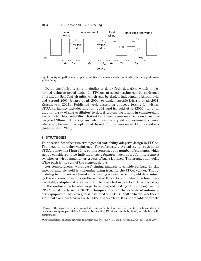
Fig. 1. A signal path is made up of a number of elements, each contributing to the signal propa-gation delay.
Delay variability testing is similar to delay fault detection, which is per-formed using at-speed tests. In FPGAs, at-speed testing can be performedby Built-In Self-Test circuits, which can be design-independent [Abramoviciand Stroud 2003; Girard et al. 2004] or design-specific [Harris et al. 2001;Krasniewski 2003]. Published work describing at-speed testing for within-FPGA variability includes Li et al. [2004] and Katsuki et al. [2006]. Li et al.used an array of ring oscillators to detect process variations in commerciallyavailable FPGAs from Xilinx. Katsuki et al. made measurements on a custom-designed 90nm LUT array, and also describe a yield enhancement scheme,whereby placement is optimised based on the measured LUT variations[Katsuki et al. 2005].
3. STRATEGIES
This section describes two strategies for variability-adaptive design in FPGAs.The focus is on delay variations. For reference, a typical signal path in anFPGA is shown in Figure 1. A path is composed of a number of elements, whichcan be considered to be individual basic features (such as LUTs, interconnectswitches or wire segments) or groups of basic features. The propagation delayof the path is the sum of the element delays.1
For completeness, “worst-case” timing analysis is considered first. In thiscase, parametric yield is a manufacturing issue for the FPGA vendor. The re-maining techniques are based on achieving a design-specific yield determinedby the end-user. It is outside the scope of this article to determine how thesevariability-adaptive strategies might be executed in practice. It is necessaryfor the end-user to be able to perform at-speed testing of the design in theFPGA, most likely using BIST techniques to avoid the expense of automatictest equipment. Moreover, it is assumed that BIST will indicate whether agiven path or circuit passes or fails the at-speed test. It is improbable that path
1Provided the signal path does not include chains of unbuffered wire segments, which would resultin a more complex path delay function. In practice, FPGA routing is buffered, so this is a validassumption.
ACM Transactions on Reconfigurable Technology and Systems, Vol. 1, No. 2, Article 10, Pub. date: June 2008.
Parametric Yield Modeling and Simulations of FPGA Circuits · 10: 5
delays would be quantified, much less delays of individual LUTs and wires,using BIST.
3.1 Worst-Case timing
The simplest timing strategy is to assign an upper bound on the value of thedelay for each path element in the die. These “worst-case” values must takeinto account all sources of variability: within-die and between dice. In speed-binned FPGAs, the delay values can be determined during at-speed testing. Ifthere is little within-die variability, testing is straightforward: each die can becharacterized by measuring the delay of a localized test structure. However,if within-die variation is a significant part of overall delay variability, the testcoverage must be either exhaustive, or at least sufficiently comprehensive toenable statistically reliable bounds on the slowest element in the die.
Using worst-case timing, all parametric yield issues are the responsibilityof the FPGA vendor; end-user designs are guaranteed to operate correctly at-speed. The designed delay for a signal path is the sum of the worst-case delaysof the individual elements. Under stochastic variation, it is improbable thatall elements in a path will exhibit near worst-case delays, making the designoverly conservative.
3.2 Statistical Static Timing Analysis
Research into statistical static timing analysis applied to FPGA designs hasonly recently begun [Lin et al. 2006]. It is instructive to examine the use ofSSTA in FPGAs, particularly as a comparison for the reconfiguration-basedtechniques described below.
Statistical static timing analysis improves on worst-case timing by takinginto account the probability that each path element has a given delay. Thedelay of a complete path can therefore be statistically described. ConventionalSTA will identify a single path in a given circuit implementation as the criticalpath, having the least slack. However, when implemented in FPGAs with sig-nificant within-die variation, the critical path may differ from device to devicebased on the variation in each die. Using SSTA, a circuit can be designed suchthat required timing is achieved at a given yield, taking into consideration allpaths, not just the path with the least nominal slack.
SSTA can be path-based or block-based. A path-based scheme examinescomplete end-to-end signal paths separately, making it highly accurate butcomputationally expensive. Block-based schemes are faster and resemble con-ventional static timing analysers, in that maximum delay values are propa-gated through leaf nodes of a path in parallel. This is less accurate as themaximum of statistically described values can in general only be estimated.
Theoretically, using SSTA in FPGAs requires at-speed testing of all end-user products. The tests would need to be specific to the end-user designs.Testing could be neglected by selecting a sufficiently high design yield, suchthat the risk of not testing is acceptably low, a decision that would be applica-tion and market dependent. This strategy, although not using the full benefitof SSTA, nevertheless would outperform worst-case timing, and would be more
ACM Transactions on Reconfigurable Technology and Systems, Vol. 1, No. 2, Article 10, Pub. date: June 2008.
10: 6 · P. Sedcole and P. Y. K. Cheung
amenable to in-field upgrades. Ultimately, statistical static timing analysis en-ables a trade-off between product parametric yield and speed.
3.3 Multiple Configurations
We now examine the class of strategies which makes use of the reconfigura-bility of the FPGA, the first of which is predicated on the use of multiple im-plementations of the same circuit design. This approach was simultaneouslyproposed by Matsumoto et al. [2007] and ourselves [Sedcole and Cheung 2007].Statistically, a given implementation of a circuit has a certain probability ofpassing at-speed testing when configured on an FPGA. If several implementa-tions of the circuit are generated, then there is an increased probability thatat least one of the implementations will meet at-speed requirements.
In this context, a circuit implementation is stored as a configuration bit-stream. All configurations are functionally identical, and could be generatedfrom the same netlist if the placement and routing of the netlist differs betweenconfigurations. Ideally, each configuration uses a different set of resources forthe critical path (or near-critical paths); if resource usage is highly correlatedbetween configurations the effectiveness of this technique is diminished.
This strategy requires a specific at-speed test for each configuration. Testsare run one by one in a given FPGA until a configuration is found which passesor all configuration options are exhausted. In the later case, the FPGA is failed.
Multiple configurations adds a degree of freedom (the number of configu-rations) to the design space, in addition to parametric yield and speed. Thedesign will therefore theoretically outperform statistical static timing analysis.
The approach has limitations. Several circuit configurations and test con-figurations must be generated and stored. Storage can be particularly prob-lematic if the strategy is implemented online in an embedded system. Designconstraints will generally preclude completely uncorrelated configurations.
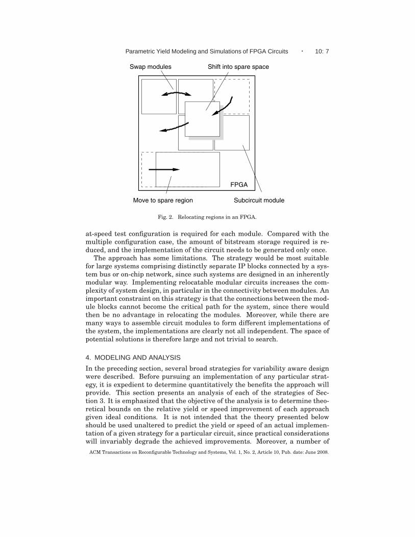
3.4 Region Relocation
The second strategy which exploits reconfiguration involves reconfiguring andrelocating parts of a complete circuit. The premise is similar to the multipleconfiguration case: different implementations of the same circuit increase theprobability that there exists one implementation that passes at-speed testing.In this case, instead of completely reconfiguring the FPGA, different configura-tions are created by partitioning the circuit into modules and then assemblingthe modules in different ways.
Different approaches to this strategy are illustrated in Figure 2. Funda-mentally, the circuit design must be sufficiently modular that critical (or near-critical) paths are encapsulated in module blocks. Moreover, the design mustsupport some degree of relocation of the modular blocks. This can include, forexample, swapping the location of modules in the FPGA, or shifting modulesinto unused areas.
With appropriate constraints on the circuit design, it is possible to storethe implemented circuit modules as partial bitstreams, and perform modulerelocation using dynamic reconfiguration [Sedcole et al. 2006]. A relocatable
ACM Transactions on Reconfigurable Technology and Systems, Vol. 1, No. 2, Article 10, Pub. date: June 2008.
Parametric Yield Modeling and Simulations of FPGA Circuits · 10: 7
Fig. 2. Relocating regions in an FPGA.
at-speed test configuration is required for each module. Compared with themultiple configuration case, the amount of bitstream storage required is re-duced, and the implementation of the circuit needs to be generated only once.
The approach has some limitations. The strategy would be most suitablefor large systems comprising distinctly separate IP blocks connected by a sys-tem bus or on-chip network, since such systems are designed in an inherentlymodular way. Implementing relocatable modular circuits increases the com-plexity of system design, in particular in the connectivity between modules. Animportant constraint on this strategy is that the connections between the mod-ule blocks cannot become the critical path for the system, since there wouldthen be no advantage in relocating the modules. Moreover, while there aremany ways to assemble circuit modules to form different implementations ofthe system, the implementations are clearly not all independent. The space ofpotential solutions is therefore large and not trivial to search.
4. MODELING AND ANALYSIS
In the preceding section, several broad strategies for variability aware designwere described. Before pursuing an implementation of any particular strat-egy, it is expedient to determine quantitatively the benefits the approach willprovide. This section presents an analysis of each of the strategies of Sec-tion 3. It is emphasized that the objective of the analysis is to determine theo-retical bounds on the relative yield or speed improvement of each approachgiven ideal conditions. It is not intended that the theory presented belowshould be used unaltered to predict the yield or speed of an actual implemen-tation of a given strategy for a particular circuit, since practical considerationswill invariably degrade the achieved improvements. Moreover, a number of
ACM Transactions on Reconfigurable Technology and Systems, Vol. 1, No. 2, Article 10, Pub. date: June 2008.
10: 8 · P. Sedcole and P. Y. K. Cheung
Table I. Notation Used in the Analysis
T Target path delayD Cumulative delay distribution
µπ Mean delay of a path π
σ 2π Variance of the delay of a path π
τ = T − µπ Target path delay relative to the meandi = µi + Xi Delay of path element i
Xi Random variable of delay of element i
Zπ =∑N
i Xi Random variable of delay of path π
N Number of elements in a pathP Number of paths in a circuitY Die yield
simplifying assumptions are made, which may not be applicable to actualimplementations, but nevertheless do not compromise the relative compar-isons between the strategies provided they are applied consistently.
In the models that follow, die-to-die variation is ignored as it can be ac-counted for by speed-binning. It is assumed that any within-die variationpresent is stochastic in nature; correlated within-die variation is negligible.This assumption is perhaps surprising given that measurements in 90nmtechnology have shown correlated variations can be significant [Sedcole andCheung 2006]. However, there are indications that at smaller geometries cor-related variability is becoming less significant [Zhao et al. 2007]. More im-portantly, the assumption is necessary for the analysis to be conservative:given that devices are speed-binned based on the their slowest attributes, anycorrelated variation would causes parts of the FPGA to operate faster than theminimum specified by the speed-bin. The pathological case that the analysismust account for is where there is no correlated variation, and all parts of thedevice operate equally slowly, except for stochastic variation. For experimentalresults verifying this assumption, see Section 5.4.
4.1 Notation
Some of the notation used in the following analysis is listed in Table I. Othernotation will be introduced as necessary. The error function, erf, has the usualdefinition:
erf(z) ≡2
√π
∫ z
0
e−x2
dx.
The complementary error function, erfc, is defined as erfc(z) ≡ 1 − erf(z).
4.2 Worst-Case Timing
An FPGA has many types of primitives which may form elemental parts ofa signal path, such as LUTs, wires, interconnect switch points, multipliers,and so on. For timing modeling, a path element is composed of the smallestinteresting segment of a signal path, such as a LUT together with the inputand output wiring. Parametric yield modeling can be applied to one or moredifferent elemental types. Assume there are K types of element of interest forparametric yield in an FPGA, Lk elements of type k, and the delay through
ACM Transactions on Reconfigurable Technology and Systems, Vol. 1, No. 2, Article 10, Pub. date: June 2008.
Parametric Yield Modeling and Simulations of FPGA Circuits · 10: 9
any given type k element is normally distributed: N(µk, σk). The cumulativeprobability distribution for the delay of a type k element is:
Dk(dk) =1
2+
1
2erf
(
dk − µk
σk
√2
)
. (1)
In this equation the variable dk is the target delay for elements of type k. Theparametric yield of an element type, Yk, is an order statistic that depends onLk, the total number of elements of that type in the FPGA. The manufacturingparametric yield of the FPGA is:
Y =
K∏
k=1
Yk =
K∏
k=1
[
Dk(dk)]Lk
. (2)
We will assume here that the yield of each elemental type is balanced, such
that Yk = Y1K . Physically, this means that a given FPGA has an equal chance
of failing to meet the manufacturing timing requirements due to a slow LUT, aslow multiplier, or a slow routing switch. This is not a necessary assumption,as it is possible to bias the yield towards a particular resource, such as LUTs.Nevertheless, it makes comparisons of the strategies more meaningful.
Given the assumption of balanced elemental yields, the designed-for delayof a signal path of N elements is:
T =N∑
i=1
di =N∑
i=1
[
µi + σi
√2 erf−1
(
2Y1
LiK − 1)]
, (3)
where the ith element has mean delay µi and variance σ 2i , dependent on its
type. Considering the specific case where parametric yield is applied to LUTsonly (for the sake of comparison) for an FPGA with L LUTs, the relative targetdelay for a given yield Y is:
T − µπ
σπ
=√
2N erf−1(
2Y1L − 1
)
. (4)
4.3 Statistical Static Timing Analysis
An ideal path-based statistical static timing analyser is examined here, whichis assumed to be able to accurately predict the actual path delays. Thus,throughout the rest of the article, SSTA is synonymous with actual path delay.
For a single path π in a given circuit implementation, with mean delay µπ
and variance σ 2π , the yield of the path will be:
Yπ = Dπ (T) =1
2+
1
2erf
(
T − µπ
σπ
√2
)
. (5)
In general, a circuit implementation will have a number of paths that willcontribute to yield loss. The impact each path has on the die yield is related tothe path delay mean and variance. For simplicity, assume that P of the pathshave sufficiently little delay slack such that they impact on yield; these we willlabel “near-critical” paths. The remaining paths in the circuit have a negligibleeffect on yield. Moreover, assume each near-critical path has the same mean
ACM Transactions on Reconfigurable Technology and Systems, Vol. 1, No. 2, Article 10, Pub. date: June 2008.
10: 10 · P. Sedcole and P. Y. K. Cheung
delay and variance, and therefore the same yield. To be consistent, the sameapproximation will be made when analysing the other strategies. The yield ofthe circuit is the product of the yields of the paths:
Y = Dπ (T)P. (6)
The relative target delay for a given yield is:
T − µπ
σπ
=√
2 erf−1(
2Y1P − 1
)
. (7)
This assumes that all the P paths are independent and separate. If thenear-critical paths share segments (because of signal path divergence or con-vergence) the yield will be higher than (6), as the effective number of paths(Peff) is lower. In the limit, Peff → 1 as the correlation between pathsapproaches unity and all critial paths converge to a single path.
4.4 Multiple Configurations
To be consistent with the SSTA evaluation, it is again assumed that a circuithas P near-critical paths, each with mean delay µπ and variance σ 2
π . The yieldof an individual path is given by (5). For a single configuration, the die yield isgiven by (6).
When multiple independent configurations are available, and the fastestconfiguration is chosen for each FPGA through at-speed testing, the circuityield is:
Y = 1 −[
1 − Dπ (T)P]C
. (8)
To derive this, note that for an FPGA to fail, it must fail at-speed tests forall C configurations. The probability that it fails for a single configuration is
1 − Dπ (T)P, and therefore to fail in all configurations[
1 − Dπ (T)P]C
.The relative target delay for a given yield is:
T − µπ
σπ
=√
2 erf−1
[
2(
1 − (1 − Y )1C
)1P − 1
]
. (9)
From (9) it is possible to determine how many independent configurationsare required to achieve a required yield Y , given a target path delay of T:
C ≥ln (1 − Y )
ln(
1 −(
u+12
)P) , (10)
where
u = erf
(
T − µπ
σπ
√2
)
. (11)
It should be emphasized that this technique, and the analysis, are depen-dent on independency of configurations. Configurations are independent if thenear-critical paths in each configuration use different resources. In practice,this will not be the case. Correlations between configurations have the effect ofreducing the effective value of C. The limiting case is where each configurationuses exactly the same resources, and the effective value of C is unity.
ACM Transactions on Reconfigurable Technology and Systems, Vol. 1, No. 2, Article 10, Pub. date: June 2008.
Parametric Yield Modeling and Simulations of FPGA Circuits · 10: 11
4.5 Region Relocation
The strategy of subdividing the circuit into many separate modular regionsthat can be assembled in different ways is next considered. Assume that themodularization of a circuit creates R identical regions and R subcircuit mod-ules, each of which can be assigned to any of the R regions. Clearly, thereare R! possible permutations for placing the subcircuits. The yield of thisstrategy is the probability of finding at least one assignment within the R!implementations where all subcircuits function (that is, pass at-speed testing).However, unlike the multiple configuration scheme, the implementations arenot independent.
Assume that the circuit is subdivided evenly into R subcircuits such thateach subcircuit has P
Rcritical paths. This we will term a balanced division.
Unbalanced divisions will be examined later.
THEOREM 4.5.1. Given a balanced subdivision of a circuit with P near-
critical paths into R subcircuit modules, and considering all possible assign-
ments of modules to regions, the yield of the system can be approximated by:
Y ≈(
1 − (1 − q)R)2R
, (12)
where
q = Dπ (T)PR =
[
1
2+
1
2erf
(
T − µπ
σπ
√2
)]PR
. (13)
Note that q is the yield of an individual subcircuit module assigned to a singleregion.
PROOF. The subdivision of the circuit is balanced. Therefore, it is reasonableto assume that any given pairing of a subcircuit and a region will have a fixedprobability of functioning, given by q in (13). The probability that a givensubcircuit does not function in a given region is (1 − q).
The yield of the region relocation scheme can be derived by determining theprobability that of the R! possible assignments of subcircuits to regions, nocombination can be found where all subcircuits function. We denote this event(that no combination works) as E. It is conjectured that E mostly occurs dueto one of two scenarios: either there a subcircuit that does not function in anyregion, or there is a region in which none of the subcircuits function. This doesnot cover all causes of E, such as there being two modules that function onlyin the same one region. Nevertheless, the probability of such cases occurringare sufficiently small that they may be ignored.
For a given subcircuit module mi, the probability that it does not function inany region (event Fmi
) is:
P(Fmi) ≡ P(mi cannot be placed) = (1 − q)R. (14)
Since there are R modules, the probability that there is a subcircuit whichcannot be placed is:
P(Fm) = P
(
⋃
i
Fmi
)
= 1 −(
1 − (1 − q)R)R
. (15)
ACM Transactions on Reconfigurable Technology and Systems, Vol. 1, No. 2, Article 10, Pub. date: June 2008.
10: 12 · P. Sedcole and P. Y. K. Cheung
Similarly, over all R regions, the probability there exists a region in which nosubcircuit works is:
P(Fr) = P
(
⋃
i
Fri
)
= 1 −(
1 − (1 − q)R)R
. (16)
where Friis the event that no subcircuit functions in region ri. The yield is
therefore:
Y = 1 − P(E) (17)
≈ 1 −(
P(Fm ∪ Fr))
(18)
≈ 1 −(
P(Fm) + P(Fr) − P(Fm)P(Fr))
, (19)
which can be reduced to (12) by substitution of (15) and (16). Note that eventsFr and Fm are only weakly dependent for large R, and so P(Fm ∩ Fr) ≈P(Fm)P(Fr).
The relative target delay given a yield Y is:
T − µπ
σπ
=√
2 erf−1
[
2
(
1 −(
1 − Y1
2R
)1R
)
RP
− 1
]
. (20)
If the subdivision of the circuit is unbalanced, the yield will be reduced.The limiting case is where all P near-critical paths are allocated to a singlesubcircuit. There are then R different placements of this subcircuit, while theplacement of the remaining subcircuits is irrelevant. The yield is then similarto the multiple configuration case:
Yunbalanced = 1 −[
1 − Dπ (T)P]R
. (21)
In practise, it may not be reasonable to have all regions and modules thesame size. An alternative may be to divide the regions and modules into twosizes: large and small. Large modules would be placed in large regions, andsmall modules in small regions. More generally, consider the case where thereare S differently sized regions. There are Ri regions of size i and Pi criticalpaths in the corresponding Ri modules. The overall timing yield can be calcu-lated from the product of each of the S independent yields:
Y =
S∏
i
Yi (22)
Yi ≈(
1 − (1 − qi)Ri)2Ri
(23)
qi = Dπ (T)PiRi =
[
1
2+
1
2erf
(
T − µπ
σπ
√2
)]
PiRi
. (24)
For the experimental results in this article, we choose to assume balancedregions of equal size.
ACM Transactions on Reconfigurable Technology and Systems, Vol. 1, No. 2, Article 10, Pub. date: June 2008.
Parametric Yield Modeling and Simulations of FPGA Circuits · 10: 13
Table II. Summary of the Analysis
SSTA Y = Dπ (T)P
Mult. conf. Y = 1 −[
1 − Dπ (T)P]C
Region reloc. Y ≈[
1 − (1 − Dπ (T)PR )R
]2R
where Dπ (T) = 12 + 1
2 erf(
T−µπ
σπ
√2
)
4.6 Summary
The derived expressions for the yields of the different strategies are summa-rized in Table II.
5. EXPERIMENTS
The theory presented in the previous section uses simple characteristic para-meters of a circuit to estimate the performance and yield of each strategy. It isassumed that the circuit has a number of independent critical paths P, each ofwhich have the same nominal delay and variance. This section describes themethodology used to apply the theory to realistic circuits, and experiments per-formed using VPR [Betz and Rose 1997]. The objectives of the experiments aretwofold. The first is to validate the theoretical results derived in the previoussection. Moreover, it is of interest to examine and compare the relative yieldenhancement offered by the alternative strategies under different conditions.
5.1 Methodology
A number of Monte Carlo simulations have been performed using the VPR soft-ware tool. The software has only been modified to gather more information onthe placement and routing than is provided by default. In particular, details ofthe specific routing resources for each path in the circuit are extracted. Thereare three types of delay elements in the abstract architecture employed byVPR: (1) LUTs, (2) global routing, and (3) local routing. Delays in global rout-ing are due to wire segments and switches connecting wire segments. Fullybuffered switches have been used in the simulations so that the delays can beisolated. Local routing delays occur from the input pin of a logic block to theinput pin of a LUT.
For this work, the deterministic timing figures produced by VPR are usedas a reference, and are chosen to be nominal (zero variation) delays. Randomdelay variations for every element type were generated for a set of 1000 dif-ferent devices. The timing for a worst-case design implementation is found byadding guard band values to the delays of every LUT, wire segment and localroute and recalculating the signal delays of all paths in the given circuit. Thedevice yield is found by comparing the guard band values with the generatedelemental variations.
The multiple configuration strategy requires many implementations of thesame circuit, with each implementation having the same timing. Unfortu-nately, VPR is designed to produce “best effort” timing results, rather than tim-ing driven by constraints. This results in a significant variation in the nominal
ACM Transactions on Reconfigurable Technology and Systems, Vol. 1, No. 2, Article 10, Pub. date: June 2008.
10: 14 · P. Sedcole and P. Y. K. Cheung
timing of the critical path produced by the tool depending on the starting con-ditions and random seed values. In contrast, a timing-constraint driven placeand route tool, when given different starting conditions and random seed val-ues, would produce designs with very similar critical path delay. To overcomethis limitation of VPR and generate implementations that more closely matchthe output of a constraint-driven tool, we produce many more implementationsof the circuit than are needed (in this case 40), initializing VPR with a differentrandom seed to generate each implementation. From these we select a subsetthat have the closest nominal critical path timing. Each implementation of thecircuit uses the same pin constraints, as would be required in a real scenario.
To simulate the region relocation strategy, we assume a large circuit madefrom several copies of one MCNC benchmark circuit. Each copy corresponds toone region. The approach artificially ensures that the circuits in each regionare all balanced. Moreover, it does not take into account any communicationthat may be required between regions. However, it is sufficient as an approx-imation at this level of examination. The circuit implementations from themultiple configuration investigation are reused for this part of the study.
The theoretical predictions for the yield of the Statistical Static TimingAnalysis, multiple configuration and region relocation strategies all use aparameter P for the number of independent critical paths in the circuit. Anestimation of P, which we will call the effective value, Peff, is calculated usingprincipal components analysis. The procedure is as follows.
(1) From the VPR implementation of a circuit, the critical path is identifiedusing the worst-case timing analysis. The nominal timing of this path isused for µπ , and the variance of the path delay σ 2
π calculated by summingthe delay variances of the path elements.
(2) Paths with nominal timing slower than a threshold of the critical pathnominal timing are identified.
(3) A correlation matrix V is constructed, where each entry Vij in the matrixis the correlation in delay between two paths πi and π j:
Vij = cor(πi, π j) =
∑
k∈Sσ 2
k
σπiσπ j
. (25)
Here, S is the set of path elements that the two paths have in common.
(4) The eigenvalues of V are calculated, and the scree test [Cattell 1966]applied to estimate the equivalent number of independent paths.
Although this method is somewhat imprecise, it provides a sufficientapproximation for Peff.
5.2 VPR Results
Here, the results of the VPR experiments are described. In all the experi-ments, the delay through any particular path element is normally distributed.The delays through each type of path element (LUTs, local routing and globalrouting) have standard deviations of 5%. All results use an FPGA model withparameters as summarized in Table III. The device size and routing channel
ACM Transactions on Reconfigurable Technology and Systems, Vol. 1, No. 2, Article 10, Pub. date: June 2008.
Parametric Yield Modeling and Simulations of FPGA Circuits · 10: 15
Table III. Summary of the Parameters of the VPR-Based Experiments
LUT size 4 inputsCluster size 4 LUTs
Routing Fully bufferedSegment length 4 logic blocks
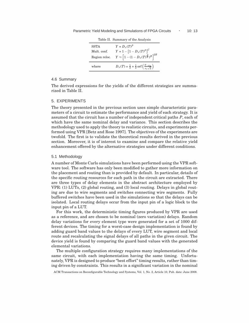
Fig. 3. The eigenvalues of the path correlation matrix V for one implementation of the alu4 circuit.Only the most significant 6% of paths are examined. A value Peff = 2 is chosen in this case.
width was set to the minimum required to reliably place and route each circuit.The input/output blocks were made dense enough to avoid the device size beinginfluenced by I/O constraints. Technology attributes were specified to ensurethat routing delays for any particular path were compariable to logic delays, tomatch the characteristics of recent FPGAs.
To start with, results from a single circuit (alu4) from the well-known MCNCbenchmark set are examined. Ten implementations (placement and routing)with similar timing were created using VPR. The eigenvalues of the equivalentindependent critical paths (which we call eigen-paths) as found by principalcomponents analysis are plotted in Figure 3. It can be seen that although thecircuit has several thousand signal paths, very few are close to the critical pathdelay. Moreover, the equivalent number of independent paths is less than 5.Applying the scree test a value of 2 is chosen for Peff in this case.
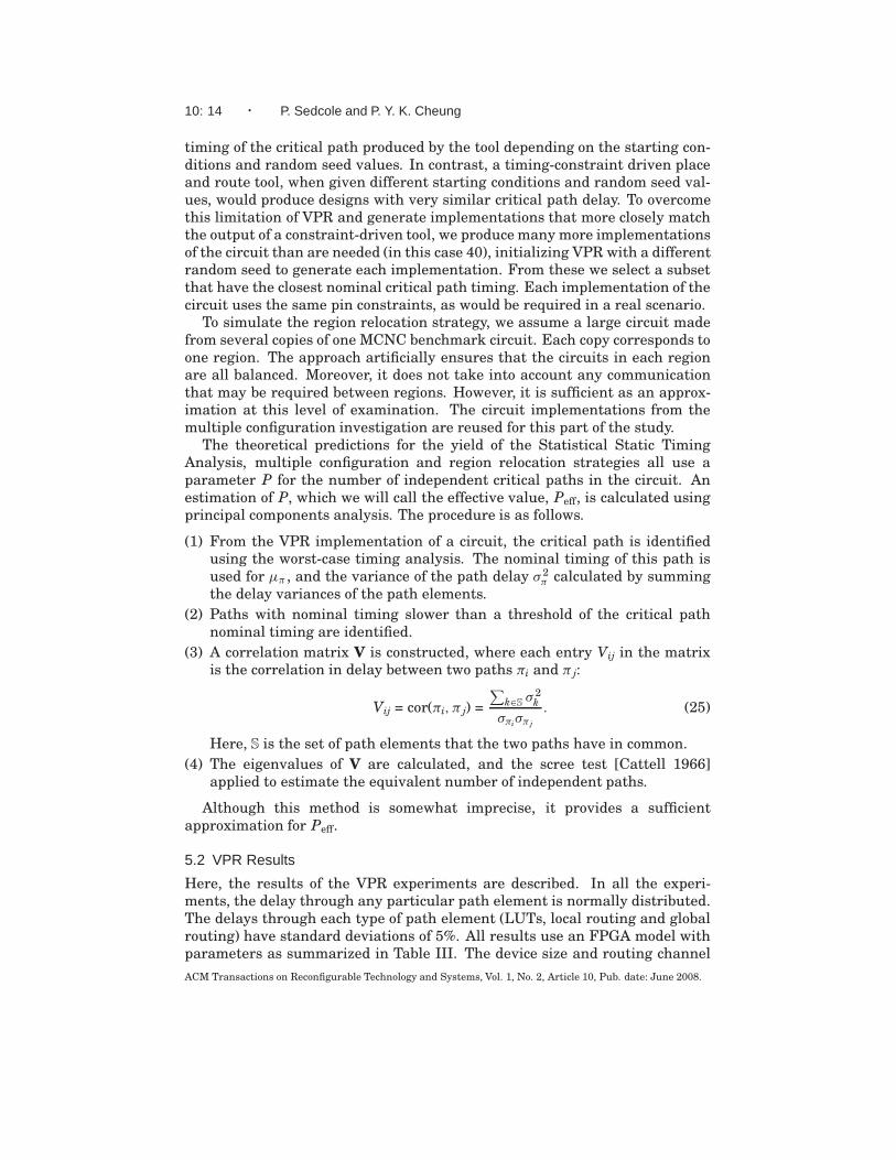
The timing yield using the worst-case design strategy is plotted for all tenimplementations of the alu4 circuit in Figure 4. The timing is normalised to
ACM Transactions on Reconfigurable Technology and Systems, Vol. 1, No. 2, Article 10, Pub. date: June 2008.
10: 16 · P. Sedcole and P. Y. K. Cheung
Fig. 4. The timing yield of ten alu4 circuit implementations using the worst-case timing strategy.The variations in each of the path element types is set at 5% standard deviation.
the nominal delay of the design, which would be achieved if there were novariability in the delays. It is important to emphasise that the curves are forthe manufacturing yield: if the FPGA vendor chooses decrease the thresholdfor the slowest acceptable elemental delay, thereby discarding more devices,the guaranteed worst-case timing will improve, but not by much. Even thoughcircuit implementations with similar timing have been selected, there is stilla spread of about ±3.4% in the circuit timing. Note that the theoreticallypredicted yield matches the yield measured from the simulations.
Using high-quality statistical timing analysis the actual delays of the im-plemented circuits can be predicted. It is assumed that SSTA is employed topredict the speed of a design after it has been placed and routed. Differentresults would be obtained by using SSTA during the place and route processas this would alter the circuit implementation. The yields of all ten imple-mentations for the actual delays are plotted in Figure 5, as well as the yieldsestimated by the theory. Here the theoretical results are sensitive to the valueof the nominal critical path delay, µπ . Nevertheless, the theory predicts theactual results well, with a mean absolute error in the delay prediction for the85% yield point of 0.23%.
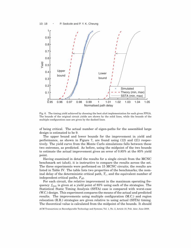
The multiple configuration strategy is examined next. From the MonteCarlo simulations, for each device the fastest of the ten implementations ischosen. The results of this are plotted in Figure 6. To generate theoreticalpredictions a single value for the nominal critical path delay µπ is needed.
ACM Transactions on Reconfigurable Technology and Systems, Vol. 1, No. 2, Article 10, Pub. date: June 2008.
Parametric Yield Modeling and Simulations of FPGA Circuits · 10: 17
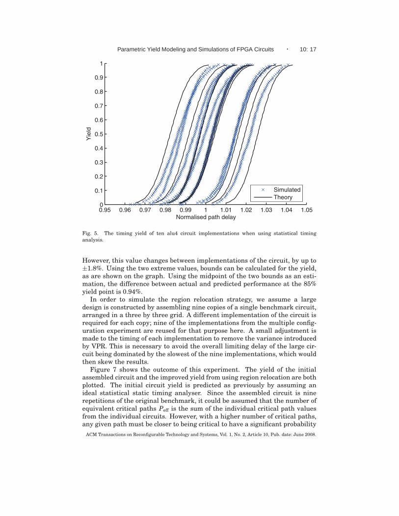
Fig. 5. The timing yield of ten alu4 circuit implementations when using statistical timinganalysis.
However, this value changes between implementations of the circuit, by up to±1.8%. Using the two extreme values, bounds can be calculated for the yield,as are shown on the graph. Using the midpoint of the two bounds as an esti-mation, the difference between actual and predicted performance at the 85%yield point is 0.94%.
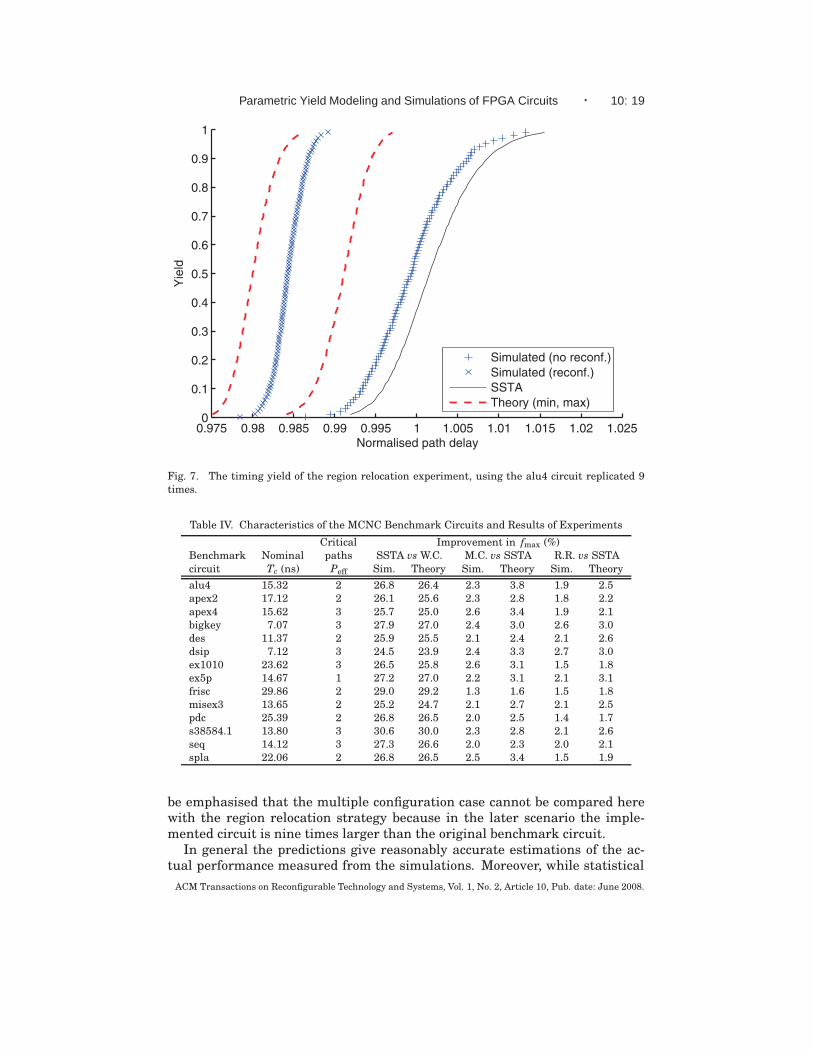
In order to simulate the region relocation strategy, we assume a largedesign is constructed by assembling nine copies of a single benchmark circuit,arranged in a three by three grid. A different implementation of the circuit isrequired for each copy; nine of the implementations from the multiple config-uration experiment are reused for that purpose here. A small adjustment ismade to the timing of each implementation to remove the variance introducedby VPR. This is necessary to avoid the overall limiting delay of the large cir-cuit being dominated by the slowest of the nine implementations, which wouldthen skew the results.
Figure 7 shows the outcome of this experiment. The yield of the initialassembled circuit and the improved yield from using region relocation are bothplotted. The initial circuit yield is predicted as previously by assuming anideal statistical static timing analyser. Since the assembled circuit is ninerepetitions of the original benchmark, it could be assumed that the number ofequivalent critical paths Peff is the sum of the individual critical path valuesfrom the individual circuits. However, with a higher number of critical paths,any given path must be closer to being critical to have a significant probability
ACM Transactions on Reconfigurable Technology and Systems, Vol. 1, No. 2, Article 10, Pub. date: June 2008.
10: 18 · P. Sedcole and P. Y. K. Cheung
Fig. 6. The timing yield achieved by choosing the best alu4 implementation for each given FPGA.The bounds of the original circuit yields are shown by the solid lines, while the bounds of themultiple configuration case are given by the dashed lines.
of being critical. The actual number of eigen-paths for the assembled largedesign is estimated to be 9.
The upper bound and lower bounds for the improvement in yield andperformance, as shown in Figure 7, are found using (12) and (21) respec-tively. The yield curve from the Monte Carlo simulations falls between thesetwo extremes, as predicted. As before, using the midpoint of the two boundsto estimate the actual improvement gives an error of 0.85% at the 85% yieldpoint.
Having examined in detail the results for a single circuit from the MCNCbenchmark set (alu4), it is instructive to compare the results across the set.The three experiments were performed on 15 MCNC circuits; the results arelisted in Table IV. The table lists two properties of the benchmarks; the nom-inal delay of the deterministic critical path, Tc, and the equivalent number ofindependent critical paths, Peff.
For each circuit, the relative improvement in the maximum operating fre-quency fmax is given at a yield point of 85% using each of the strategies. TheStatistical Static Timing Analysis (SSTA) case is compared with worst-case(W.C.) design. This experiment compares the means of the actual and predictedresults. The improvements using multiple configuration (M.C.) and regionrelocation (R.R.) strategies are given relative to using actual (SSTA) timing.The theoretical value is calculated from the midpoint of the bounds. It should
ACM Transactions on Reconfigurable Technology and Systems, Vol. 1, No. 2, Article 10, Pub. date: June 2008.
Parametric Yield Modeling and Simulations of FPGA Circuits · 10: 19
Fig. 7. The timing yield of the region relocation experiment, using the alu4 circuit replicated 9times.
Table IV. Characteristics of the MCNC Benchmark Circuits and Results of Experiments
Critical Improvement in fmax (%)Benchmark Nominal paths SSTA vs W.C. M.C. vs SSTA R.R. vs SSTA
circuit Tc (ns) Peff Sim. Theory Sim. Theory Sim. Theory
alu4 15.32 2 26.8 26.4 2.3 3.8 1.9 2.5apex2 17.12 2 26.1 25.6 2.3 2.8 1.8 2.2
apex4 15.62 3 25.7 25.0 2.6 3.4 1.9 2.1bigkey 7.07 3 27.9 27.0 2.4 3.0 2.6 3.0des 11.37 2 25.9 25.5 2.1 2.4 2.1 2.6dsip 7.12 3 24.5 23.9 2.4 3.3 2.7 3.0ex1010 23.62 3 26.5 25.8 2.6 3.1 1.5 1.8ex5p 14.67 1 27.2 27.0 2.2 3.1 2.1 3.1frisc 29.86 2 29.0 29.2 1.3 1.6 1.5 1.8misex3 13.65 2 25.2 24.7 2.1 2.7 2.1 2.5pdc 25.39 2 26.8 26.5 2.0 2.5 1.4 1.7s38584.1 13.80 3 30.6 30.0 2.3 2.8 2.1 2.6seq 14.12 3 27.3 26.6 2.0 2.3 2.0 2.1spla 22.06 2 26.8 26.5 2.5 3.4 1.5 1.9
be emphasised that the multiple configuration case cannot be compared herewith the region relocation strategy because in the later scenario the imple-mented circuit is nine times larger than the original benchmark circuit.
In general the predictions give reasonably accurate estimations of the ac-tual performance measured from the simulations. Moreover, while statistical
ACM Transactions on Reconfigurable Technology and Systems, Vol. 1, No. 2, Article 10, Pub. date: June 2008.
10: 20 · P. Sedcole and P. Y. K. Cheung
Fig. 8. The yields using actual timing for six of the MCNC benchmark circuits. These simulatedresults show that timing is less effected by variability in circuits that have longer critical paths.
timing analysis gives a significant gain in performance, the gain from usingreconfiguration is incremental in these results.
5.3 Exploration
Performing experiments using benchmark circuits give credence to the predic-tions of the probabilistic analysis. However, it is also of interest to examinethe impact that different parameters have on the outcome of the strategies,as well as making a comparison of statistical timing analysis with the two re-configuration based approaches. For these purposes the theoretical model isinvaluable.
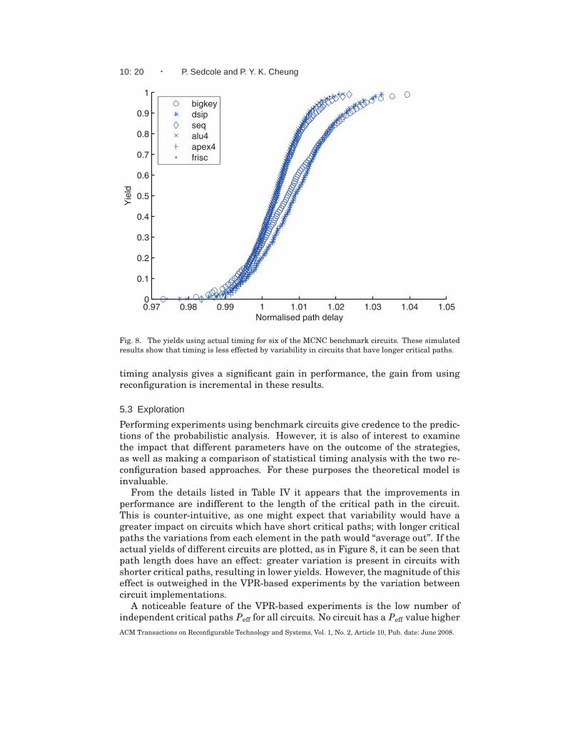
From the details listed in Table IV it appears that the improvements inperformance are indifferent to the length of the critical path in the circuit.This is counter-intuitive, as one might expect that variability would have agreater impact on circuits which have short critical paths; with longer criticalpaths the variations from each element in the path would “average out”. If theactual yields of different circuits are plotted, as in Figure 8, it can be seen thatpath length does have an effect: greater variation is present in circuits withshorter critical paths, resulting in lower yields. However, the magnitude of thiseffect is outweighed in the VPR-based experiments by the variation betweencircuit implementations.
A noticeable feature of the VPR-based experiments is the low number ofindependent critical paths Peff for all circuits. No circuit has a Peff value higher
ACM Transactions on Reconfigurable Technology and Systems, Vol. 1, No. 2, Article 10, Pub. date: June 2008.
Parametric Yield Modeling and Simulations of FPGA Circuits · 10: 21
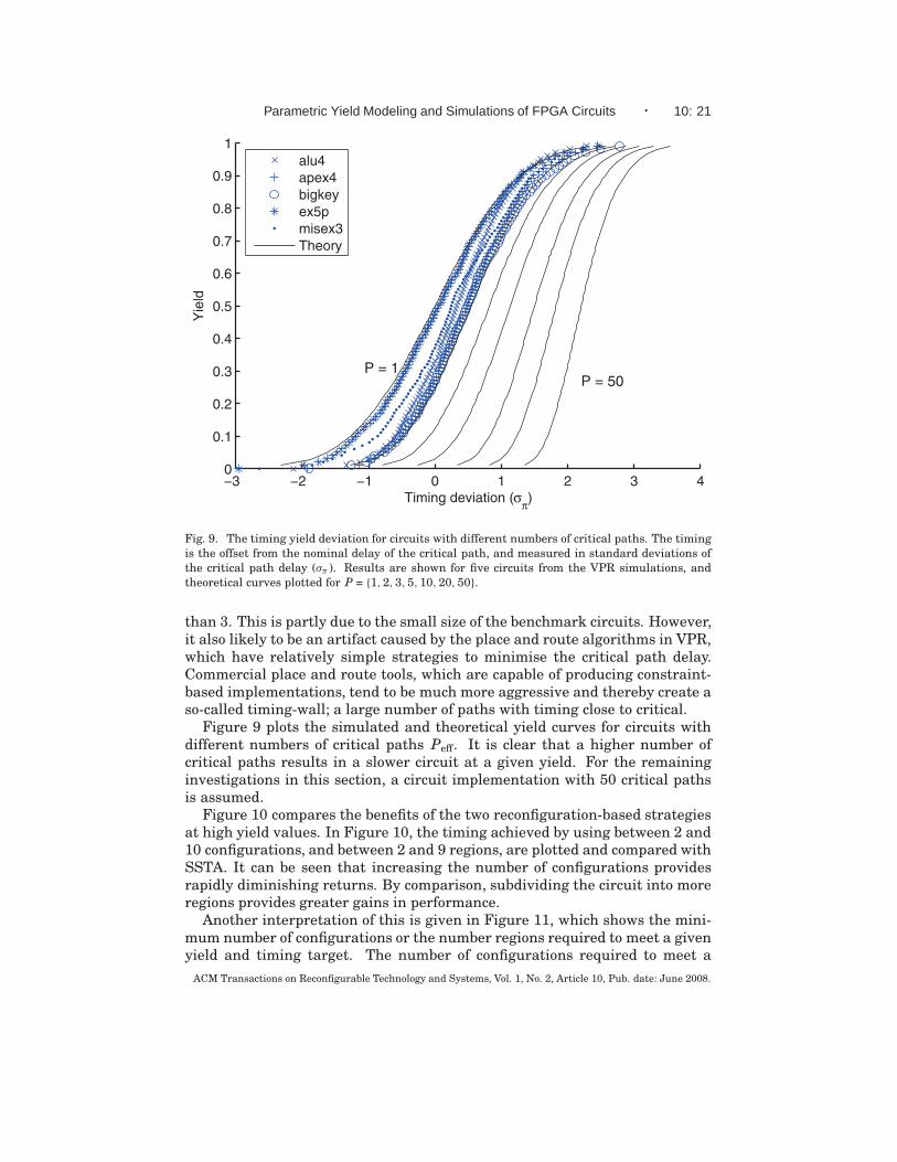
Fig. 9. The timing yield deviation for circuits with different numbers of critical paths. The timingis the offset from the nominal delay of the critical path, and measured in standard deviations ofthe critical path delay (σπ ). Results are shown for five circuits from the VPR simulations, andtheoretical curves plotted for P = {1,2, 3, 5, 10, 20, 50}.
than 3. This is partly due to the small size of the benchmark circuits. However,it also likely to be an artifact caused by the place and route algorithms in VPR,which have relatively simple strategies to minimise the critical path delay.Commercial place and route tools, which are capable of producing constraint-based implementations, tend to be much more aggressive and thereby create aso-called timing-wall; a large number of paths with timing close to critical.
Figure 9 plots the simulated and theoretical yield curves for circuits withdifferent numbers of critical paths Peff. It is clear that a higher number ofcritical paths results in a slower circuit at a given yield. For the remaininginvestigations in this section, a circuit implementation with 50 critical pathsis assumed.
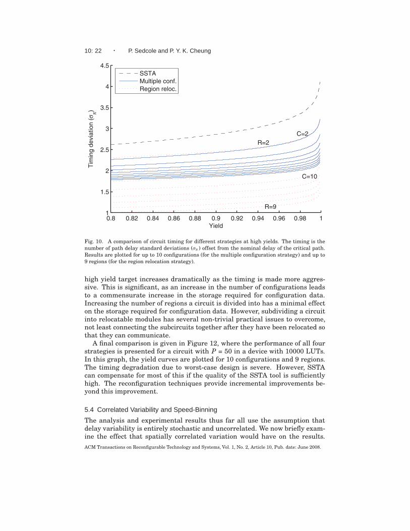
Figure 10 compares the benefits of the two reconfiguration-based strategiesat high yield values. In Figure 10, the timing achieved by using between 2 and10 configurations, and between 2 and 9 regions, are plotted and compared withSSTA. It can be seen that increasing the number of configurations providesrapidly diminishing returns. By comparison, subdividing the circuit into moreregions provides greater gains in performance.
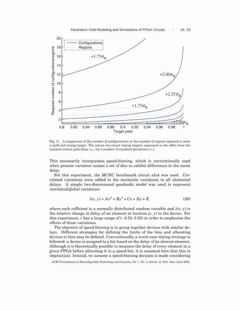
Another interpretation of this is given in Figure 11, which shows the mini-mum number of configurations or the number regions required to meet a givenyield and timing target. The number of configurations required to meet a
ACM Transactions on Reconfigurable Technology and Systems, Vol. 1, No. 2, Article 10, Pub. date: June 2008.
10: 22 · P. Sedcole and P. Y. K. Cheung
Fig. 10. A comparison of circuit timing for different strategies at high yields. The timing is thenumber of path delay standard deviations (σπ ) offset from the nominal delay of the critical path.Results are plotted for up to 10 configurations (for the multiple configuration strategy) and up to9 regions (for the region relocation strategy).
high yield target increases dramatically as the timing is made more aggres-sive. This is significant, as an increase in the number of configurations leadsto a commensurate increase in the storage required for configuration data.Increasing the number of regions a circuit is divided into has a minimal effecton the storage required for configuration data. However, subdividing a circuitinto relocatable modules has several non-trivial practical issues to overcome,not least connecting the subcircuits together after they have been relocated sothat they can communicate.
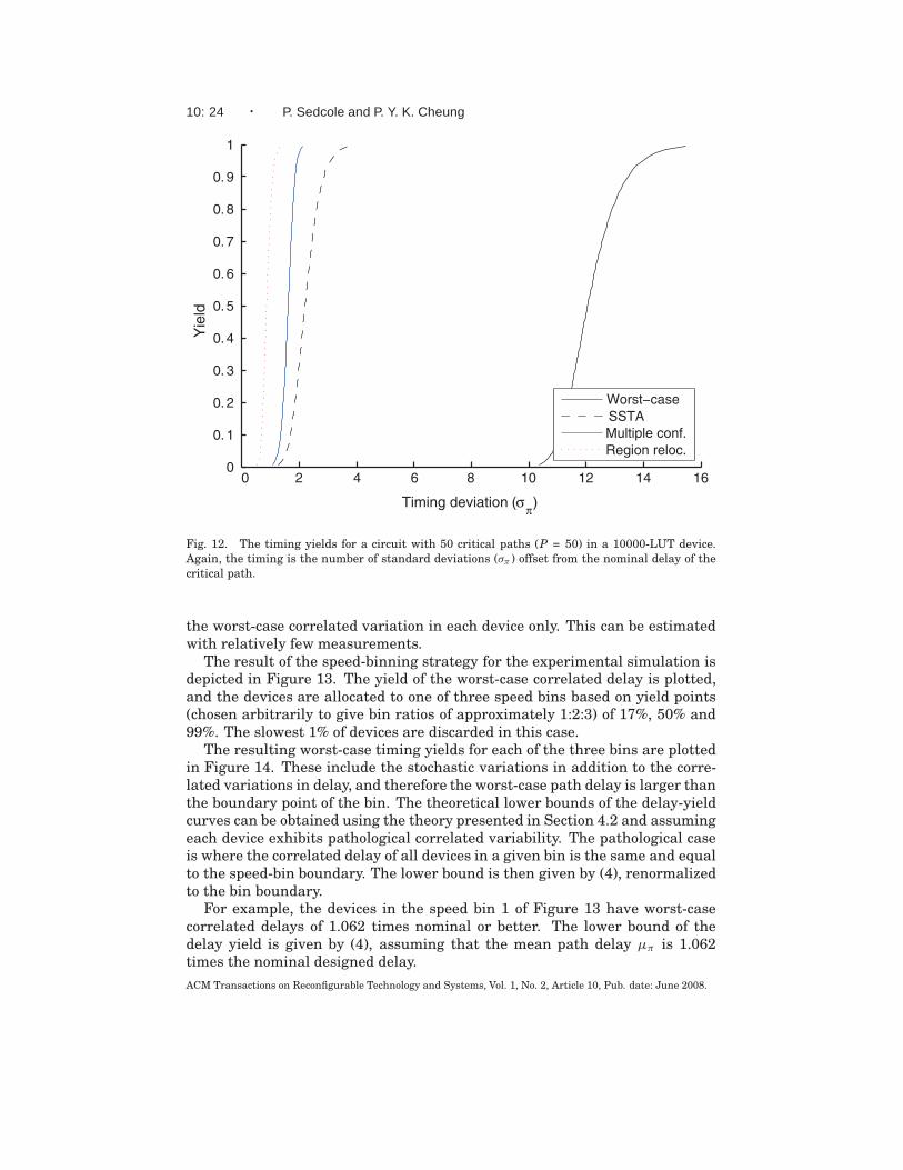
A final comparison is given in Figure 12, where the performance of all fourstrategies is presented for a circuit with P = 50 in a device with 10000 LUTs.In this graph, the yield curves are plotted for 10 configurations and 9 regions.The timing degradation due to worst-case design is severe. However, SSTAcan compensate for most of this if the quality of the SSTA tool is sufficientlyhigh. The reconfiguration techniques provide incremental improvements be-yond this improvement.
5.4 Correlated Variability and Speed-Binning
The analysis and experimental results thus far all use the assumption thatdelay variability is entirely stochastic and uncorrelated. We now briefly exam-ine the effect that spatially correlated variation would have on the results.
ACM Transactions on Reconfigurable Technology and Systems, Vol. 1, No. 2, Article 10, Pub. date: June 2008.
Parametric Yield Modeling and Simulations of FPGA Circuits · 10: 23
Fig. 11. A comparison of the number of configurations or the number of regions required to meeta yield and timing target. The curves are circuit timing targets, expressed in the offset from thenominal critical path delay (µπ ) by a number of standard deviations (σπ ).
This necessarily incorporates speed-binning, which is conventionally usedwhen process variation causes a set of dice to exhibit differences in the meandelay.
For this experiment, the MCNC benchmark circuit alu4 was used. Cor-related variations were added to the stochastic variations in all elementaldelays. A simple two-dimensional quadradic model was used to representcorrelated/global variations:
δ(x, y) = Ax2 + By2 + Cx + Dy + E, (26)
where each cofficient is a normally distributed random variable and δ(x, y) isthe relative change in delay of an element at location (x, y) in the device. Forthis experiment, δ has a large range of (−0.55, 0.53) in order to emphasise theeffects of these variations.
The objective of speed-binning is to group together devices with similar de-lays. Different strategies for defining the limits of the bins and allocatingdevices to bins may be defined. Conventionally, a worst-case timing strategy isfollowed: a device is assigned to a bin based on the delay of its slowest element.Although it is theoretically possible to measure the delay of every element in agiven FPGA before allocating it to a speed-bin, it is assumed here that this isimpractical. Instead, we assume a speed-binning decision is made considering
ACM Transactions on Reconfigurable Technology and Systems, Vol. 1, No. 2, Article 10, Pub. date: June 2008.
10: 24 · P. Sedcole and P. Y. K. Cheung
Fig. 12. The timing yields for a circuit with 50 critical paths (P = 50) in a 10000-LUT device.Again, the timing is the number of standard deviations (σπ ) offset from the nominal delay of thecritical path.
the worst-case correlated variation in each device only. This can be estimatedwith relatively few measurements.
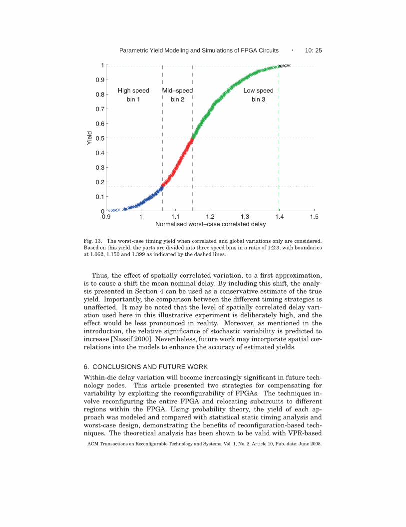
The result of the speed-binning strategy for the experimental simulation isdepicted in Figure 13. The yield of the worst-case correlated delay is plotted,and the devices are allocated to one of three speed bins based on yield points(chosen arbitrarily to give bin ratios of approximately 1:2:3) of 17%, 50% and99%. The slowest 1% of devices are discarded in this case.
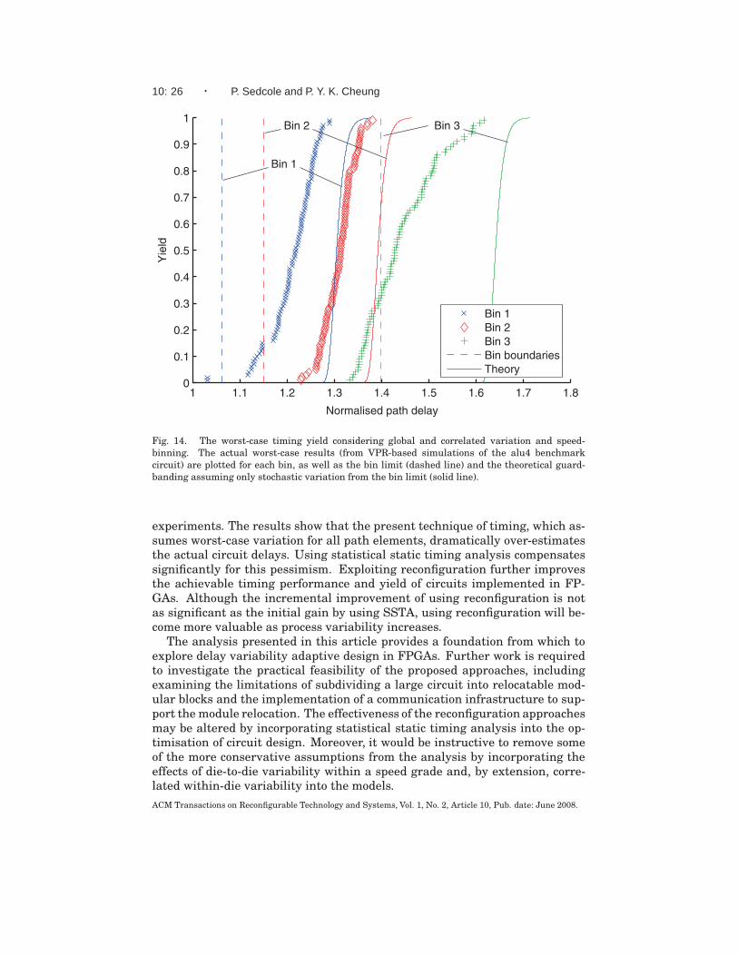
The resulting worst-case timing yields for each of the three bins are plottedin Figure 14. These include the stochastic variations in addition to the corre-lated variations in delay, and therefore the worst-case path delay is larger thanthe boundary point of the bin. The theoretical lower bounds of the delay-yieldcurves can be obtained using the theory presented in Section 4.2 and assumingeach device exhibits pathological correlated variability. The pathological caseis where the correlated delay of all devices in a given bin is the same and equalto the speed-bin boundary. The lower bound is then given by (4), renormalizedto the bin boundary.
For example, the devices in the speed bin 1 of Figure 13 have worst-casecorrelated delays of 1.062 times nominal or better. The lower bound of thedelay yield is given by (4), assuming that the mean path delay µπ is 1.062times the nominal designed delay.
ACM Transactions on Reconfigurable Technology and Systems, Vol. 1, No. 2, Article 10, Pub. date: June 2008.
Parametric Yield Modeling and Simulations of FPGA Circuits · 10: 25
Fig. 13. The worst-case timing yield when correlated and global variations only are considered.Based on this yield, the parts are divided into three speed bins in a ratio of 1:2:3, with boundariesat 1.062, 1.150 and 1.399 as indicated by the dashed lines.
Thus, the effect of spatially correlated variation, to a first approximation,is to cause a shift the mean nominal delay. By including this shift, the analy-sis presented in Section 4 can be used as a conservative estimate of the trueyield. Importantly, the comparison between the different timing strategies isunaffected. It may be noted that the level of spatially correlated delay vari-ation used here in this illustrative experiment is deliberately high, and theeffect would be less pronounced in reality. Moreover, as mentioned in theintroduction, the relative significance of stochastic variability is predicted toincrease [Nassif 2000]. Nevertheless, future work may incorporate spatial cor-relations into the models to enhance the accuracy of estimated yields.
6. CONCLUSIONS AND FUTURE WORK
Within-die delay variation will become increasingly significant in future tech-nology nodes. This article presented two strategies for compensating forvariability by exploiting the reconfigurability of FPGAs. The techniques in-volve reconfiguring the entire FPGA and relocating subcircuits to differentregions within the FPGA. Using probability theory, the yield of each ap-proach was modeled and compared with statistical static timing analysis andworst-case design, demonstrating the benefits of reconfiguration-based tech-niques. The theoretical analysis has been shown to be valid with VPR-based
ACM Transactions on Reconfigurable Technology and Systems, Vol. 1, No. 2, Article 10, Pub. date: June 2008.
10: 26 · P. Sedcole and P. Y. K. Cheung
Fig. 14. The worst-case timing yield considering global and correlated variation and speed-binning. The actual worst-case results (from VPR-based simulations of the alu4 benchmarkcircuit) are plotted for each bin, as well as the bin limit (dashed line) and the theoretical guard-banding assuming only stochastic variation from the bin limit (solid line).
experiments. The results show that the present technique of timing, which as-sumes worst-case variation for all path elements, dramatically over-estimatesthe actual circuit delays. Using statistical static timing analysis compensatessignificantly for this pessimism. Exploiting reconfiguration further improvesthe achievable timing performance and yield of circuits implemented in FP-GAs. Although the incremental improvement of using reconfiguration is notas significant as the initial gain by using SSTA, using reconfiguration will be-come more valuable as process variability increases.
The analysis presented in this article provides a foundation from which toexplore delay variability adaptive design in FPGAs. Further work is requiredto investigate the practical feasibility of the proposed approaches, includingexamining the limitations of subdividing a large circuit into relocatable mod-ular blocks and the implementation of a communication infrastructure to sup-port the module relocation. The effectiveness of the reconfiguration approachesmay be altered by incorporating statistical static timing analysis into the op-timisation of circuit design. Moreover, it would be instructive to remove someof the more conservative assumptions from the analysis by incorporating theeffects of die-to-die variability within a speed grade and, by extension, corre-lated within-die variability into the models.
ACM Transactions on Reconfigurable Technology and Systems, Vol. 1, No. 2, Article 10, Pub. date: June 2008.
Parametric Yield Modeling and Simulations of FPGA Circuits · 10: 27
ACKNOWLEDGMENT
Thanks to Dr. R. Sedcole for advice and suggestions on statistical theory.
REFERENCES
ABRAMOVICI, M. AND STROUD, C. E. 2003. BIST-based delay-fault testing in FPGAs. J. Electr.
Test.: Theory Appl. 19, 5, 549–558.
ASENOV, A., KAYA, S., AND BROWN, A. R. 2003. Intrinsic parameter fluctuations in decananome-ter MOSFETs introduced by gate line edge roughness. IEEE Trans. Electr. Devices 50, 5,1254–1260.
ASENOV, A., KAYA, S., AND DAVIES, J. H. 2002. Intrinsic threshold voltage fluctuationsindecananometer MOSFETs due to local oxide thickness variations. IEEE Trans. Electr. De-
vices 49, 6, 112–119.
BETZ, V. AND ROSE, J. 1997. VPR: A new packing, placement and routing tool for FPGA research.In Proceedings of the Field-Programmable Logic and Applications. Springer.
CAO, Y., GUPTA, P., KAHNG, A. B., SYLVESTER, D., AND YANG, J. 2002. Design sensitivities tovariability: Extrapolations and assessments in nanometer VLSI. In Proceedings of the IEEE
International ASIC/SOC Conference.
CATTELL, R. B. 1966. The scree test for the number of factors. Multivariate Behav. Resear. 1,245–276.
CHANG, H., ZOLOTOV, V., NARAYAN, S., AND VISWESWARIAH, C. 2005. Parameterized block-based statistical timing analysis with non-Gaussian parameters, nonlinear delay functions. InProceedings of the Design Automation Conference.
GIRARD, P., HERON, O., PRAVOSSOUDOVITCH, S., AND RENOVELL, M. 2004. High quality TPGfor delay faults in look-up tables of FPGAs. In Proceedings of the IEEE International Workshop
on Electronic Design, Test and Applications.
HARRIS, I. G., MENON, P. R., AND TESSIER, R. 2001. BIST-based delay path testing in FPGAarchitectures. In Proceedings of the IEEE International Test Conference.
KATSUKI, K., KOTANI, M., KOBAYASHI, K., AND ONODERA, H. 2005. A yield and speed enhance-ment scheme under within-die variations on 90nm LUT array. In Proceedings of the IEEE Cus-
tom Integrated Circuits Conference.
KATSUKI, K., KOTANI, M., KOBAYASHI, K., AND ONODERA, H. 2006. Measurement results ofwithin-die variations on a 90nm LUT array for speed and yield enhancement of reconfigurabledevices. In Proceedings of the Asia and South Pacific Design Automation Conference.
KIM, K. S., MITRA, S., AND RYAN, P. G. 2003. Delay defect characteristics and testing strategies.IEEE Design Test Comput. 20, 5, 8–16.
KRASNIEWSKI, A. 2003. Evaluation of testability of path delay faults for user-configured program-mable devices. In Proceedings of the Field-Programmable Logic and Applications. IEEE.
LI, X.-Y., WANG, F., LA, T., AND LING, Z.-M. 2004. FPGA as process monitor–an effective methodto characterize poly gate CD variation and its impact on product performance and yield. IEEE
Trans. Semicond. Manuf. 17, 3, 267–272.
LIN, Y., HUTTON, M., AND HE, L. 2006. Placement and timing for FPGAs considering variations.In Proceedings of the Field-Programmable Logic and Applications. IEEE.
MATSUMOTO, Y., HIOKI, M., KAWANAMI, T., TSUTSUMI, T., NAKAGAWA, T., SEKIGAWA, T., AND
KOIKE, H. 2007. Performance and yield enhancement of FPGAs with within-die variation usingmultiple configurations. In Proceedings of the ACM/SIGDA International Symposium on Field
Programmable Gate Arrays. ACM.
NABAA, G., AZIZI, N., AND NAJM, F. N. 2006. An adaptive FPGA architecture with process vari-ation compensation and reduced leakage. In Proceedings of the Design Automation Conference.
NASSIF, S. R. 2000. Design for variability in DSM technologies. In Proceedings of the IEEE Inter-
national Symposium on Quality Electronic Design.
SEDCOLE, P., BLODGET, B., BECKER, T., ANDERSON, J., AND LYSAGHT, P. 2006. Modular dy-namic reconfiguration in Virtex FPGAs. IEE Proc. Comput. Digital Techniq. 153, 3, 157–164.
ACM Transactions on Reconfigurable Technology and Systems, Vol. 1, No. 2, Article 10, Pub. date: June 2008.
10: 28 · P. Sedcole and P. Y. K. Cheung
SEDCOLE, P. AND CHEUNG, P. Y. K. 2006. Within-die delay variability in 90nm FPGAs and be-yond. In Proceedings of the IEEE International Conference on Field Programmable Technology.
SEDCOLE, P. AND CHEUNG, P. Y. K. 2007. Parametric yield in FPGAs due to within-die delay vari-ations: A quantitative analysis. In Proceedings of the ACM/SIGDA International Symposium on
Field Programmable Gate Arrays. ACM.
VISWESWARIAH, C. 2003. Death, taxes and failing chips. In Proceedings of the Design Automation
Conference.
VISWESWARIAH, C., RAVINDRAN, K., KALAFALA, K., WALKER, S. G., AND NARAYAN, S. 2004.First-order incremental block-based statistical timing analysis. In Proceedings of the Design
Automation Conference.
WONG, H.-Y., CHENG, L., LIN, Y., AND HE, L. 2005. FPGA device and architecture evaluationconsidering process variation. In Proceedings of the International Conference on Computer-Aided
Design.
ZHAO, W., LIU, F., AGARWAL, K., ACHARYYA, D., NASSIF, S., NOWKA, K., AND CAO, Y. 2007.Rigorous extraction of process variations for 65nm CMOS design. In Proceedings of the European
Solid-State Circuits Conference.
Received May 2007; revised September 2007, January 2008; accepted April 2008
ACM Transactions on Reconfigurable Technology and Systems, Vol. 1, No. 2, Article 10, Pub. date: June 2008.