part-b: simulation using pspice software
TRANSCRIPT

Dr. Ambedkar Institute of Technology Analog Electronics Circuits Laboratory Manual 18ECL36
Department of Electronics and Communication Engineering Page | 31
PART-B: Simulation using PSpice software Experiment No. B.1
B. 1: Design and verification of voltage follower, inverting amplifier and non-inverting amplifier
using OP-AMP B. 1.1: Voltage Follower Aim: - Design and Verification of OP-AMP as Voltage Follower
Circuit Diagram: OPAMP as Voltage Follower
Figure 1.1: Voltage Follower Circuit
Steps to build the Circuit Diagram in PSpice simulation:
1. Click on the Schematics icon on the Desktop to open the Simulation window.
Dr. Ambedkar Institute of Technology Analog Electronics Circuits Laboratory Manual 18ECL36
Department of Electronics and Communication Engineering Page | 32
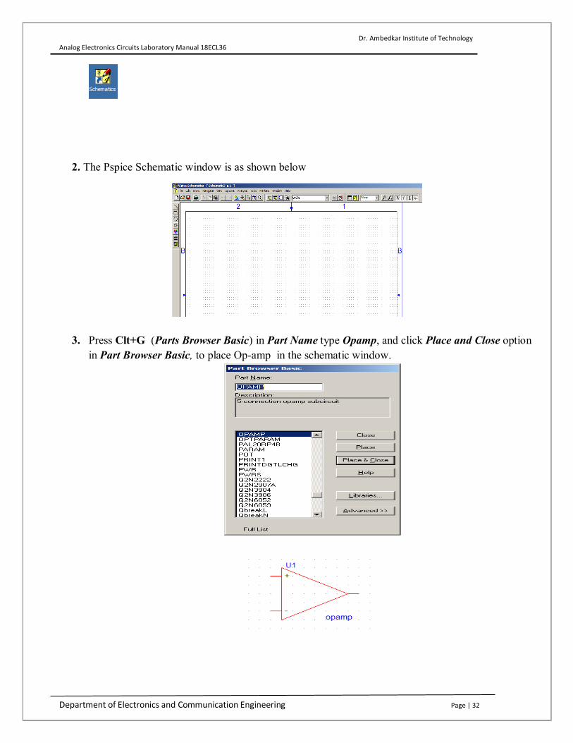
2. The Pspice Schematic window is as shown below
3. Press Clt+G (Parts Browser Basic) in Part Name type Opamp, and click Place and Close option in Part Browser Basic, to place Op-amp in the schematic window.

Dr. Ambedkar Institute of Technology Analog Electronics Circuits Laboratory Manual 18ECL36
Department of Electronics and Communication Engineering Page | 33
4. Press Clt+G (Parts Browser Basic) to select input sine wave, in the Part Name type vsin , and
click Place and Close option in Part Browser Basic, to place vsin schematic window.
vsin icon
5. Double click on the vsin icon to add the following parameter. (Note: Each time adding the parameter always press, Save Attr ) a. DC =0 b. AC =0 c. VOFF=0 d. VAMPL =0.5v e. FREQ = 50Hz

Dr. Ambedkar Institute of Technology Analog Electronics Circuits Laboratory Manual 18ECL36
Department of Electronics and Communication Engineering Page | 34
6. Select Draw wire option from menu bar to connect wire .
7. Select Draw wire option from menu bar to connect wire between the positive of the sine wave is
connected to the non-inverting terminal of op-amp (‘ – sign’ is non- inverting terminal of op-amp) and negative sign to ground, using draw wire option, connect the wires between the positive input terminal and negative ground terminal .
8. To get ground icon, Press Clt+G (Parts Browser Basic) to select ground icon in the Part Name type gnd_earth , and click Place and Close option in Part Browser Basic, to place ground in schematic window
Ground Icon
9. Using draw wire option, connect the wires between the inverting terminal of op-amp (‘ + sign’
is inverting terminal of op-amp) to the output of opamp, connect a wire using draw wire at output, to set as output label point.
10. Double click on the output label point to label as vout.

Dr. Ambedkar Institute of Technology Analog Electronics Circuits Laboratory Manual 18ECL36
Department of Electronics and Communication Engineering Page | 35
11. To perform simulation, the transient analysis must be setup.
12. Click on Analysis in the menu bar, select Setup option.
13. In Analysis Setup, click on Transient label.
Dr. Ambedkar Institute of Technology Analog Electronics Circuits Laboratory Manual 18ECL36
Department of Electronics and Communication Engineering Page | 36
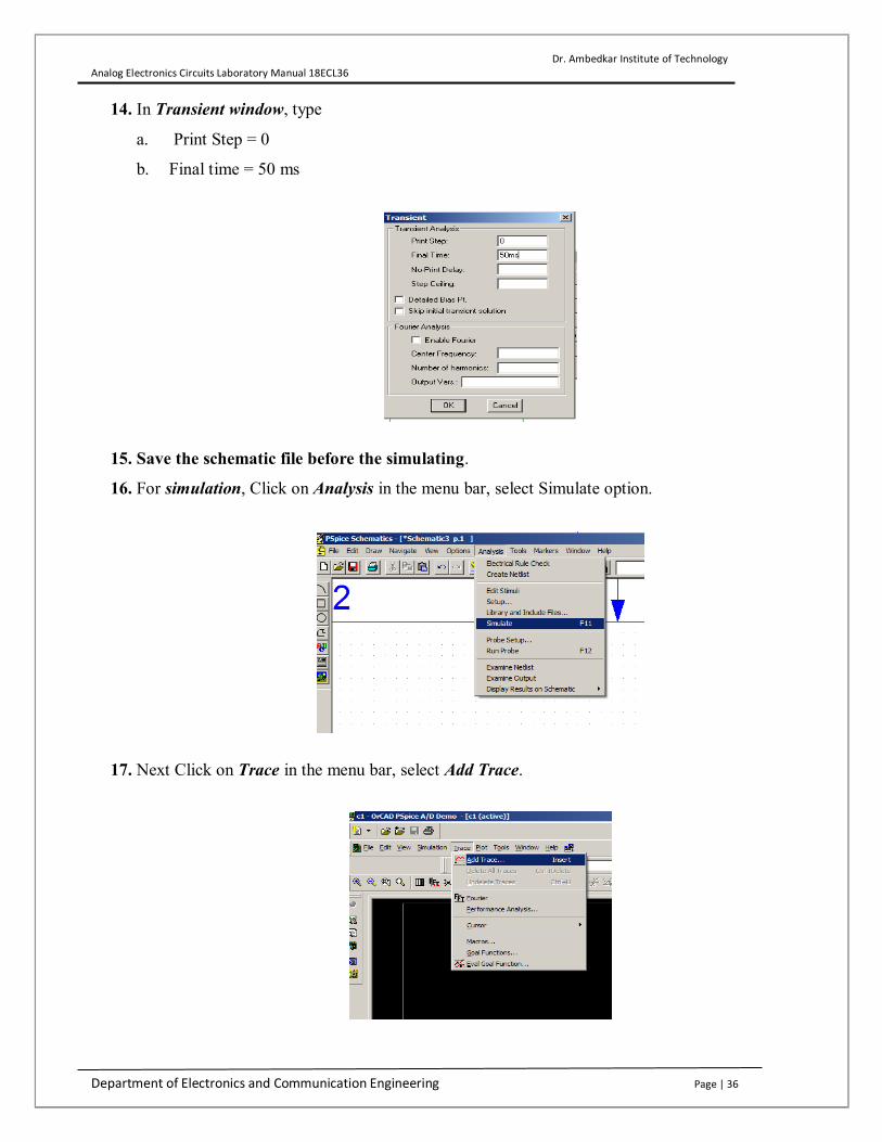
14. In Transient window, type
a. Print Step = 0
b. Final time = 50 ms
15. Save the schematic file before the simulating.
16. For simulation, Click on Analysis in the menu bar, select Simulate option.
17. Next Click on Trace in the menu bar, select Add Trace.
Dr. Ambedkar Institute of Technology Analog Electronics Circuits Laboratory Manual 18ECL36
Department of Electronics and Communication Engineering Page | 37
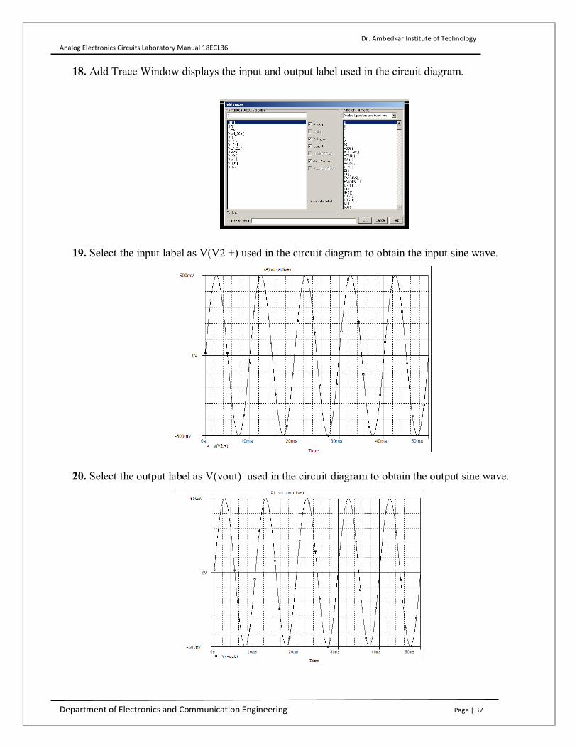
18. Add Trace Window displays the input and output label used in the circuit diagram.
19. Select the input label as V(V2 +) used in the circuit diagram to obtain the input sine wave.
20. Select the output label as V(vout) used in the circuit diagram to obtain the output sine wave.

Dr. Ambedkar Institute of Technology Analog Electronics Circuits Laboratory Manual 18ECL36
Department of Electronics and Communication Engineering Page | 38
21. The output wave follows the input wave, the amplitude of the output to the input wave is the
same, and hence gain = unity
22. The circuit opamp as voltage follower is simulated.
B. 1.2: Inverting Amplifier Aim: - Design and verification of OP-AMP as Inverting Amplifier Circuit Diagram: OPAMP as Inverting Amplifier
Figure 1.2: Inverting Amplifier Circuit
Design:

Dr. Ambedkar Institute of Technology Analog Electronics Circuits Laboratory Manual 18ECL36
Department of Electronics and Communication Engineering Page | 39
Steps to build the Circuit Diagram in PSpice simulation:
1. Press Clt+G (Parts Browser Basic) in Part Name type Opamp, and click Place and Close option in Part Browser Basic, to place Op-amp in the schematic window.
2. Press Clt+G (Parts Browser Basic) to select input sine wave, in the Part Name type vsin , and
click Place and Close option in Part Browser Basic, to place vsin schematic window.
3. Double click on the vsin icon to add the following parameter
(Note: Each time adding the parameter always press, Save Attr ) Name of the input sine wave = Vin a. DC =0
b. AC =0
c. VOFF=0
d. VAMPL =0.5v
e. FREQ = 1KHz
4. The positive of the sine wave is connected to the inverting terminal of op-amp (‘ + sign’ is
inverting terminal of op-amp) and negative sign to ground, using draw wire option, connect the wires between the positive input terminal and negative ground terminal.
5. Press Clt+G (Parts Browser Basic) to select resistors, in the Part Name type ‘r’ , and click Place and Close option in Part Browser Basic, to place resistors in the schematic window.

Dr. Ambedkar Institute of Technology Analog Electronics Circuits Laboratory Manual 18ECL36
Department of Electronics and Communication Engineering Page | 40
6. Double click on the resistor icon to add the following parameter .
a. R1 = 10K
b. R2= 50K
7. Select Draw wire option from menu bar to connect wire between inverting terminal ( ‘+ sign’ is inverting terminal of op-amp) and to R1 resistors , and R2 resistors and output , the label the output name as invoutput.
8. In Transient window, type a. Print Step = 0 b. Final time = 5 ms
9. Click on Analysis in the menu bar, select Simulate option, next Click on Trace in the menu bar, select Add Trace. Add Trace Window displays the input and output label used in the circuit diagram.
10. Select the input label as V1(Vin) used in the circuit diagram to obtain the input sine wave

Dr. Ambedkar Institute of Technology Analog Electronics Circuits Laboratory Manual 18ECL36
Department of Electronics and Communication Engineering Page | 41
11. Select the output as V(invoutput) used in the circuit diagram to obtain the input sine wave.

Dr. Ambedkar Institute of Technology Analog Electronics Circuits Laboratory Manual 18ECL36
Department of Electronics and Communication Engineering Page | 42
The output vs the input wave is observed, which shows the output wave is phase shift w.r.t to the input sine wave, with Vout = - 1.25 V
The circuit opamp as inverting amplifier is simulated.
Dr. Ambedkar Institute of Technology Analog Electronics Circuits Laboratory Manual 18ECL36
Department of Electronics and Communication Engineering Page | 43
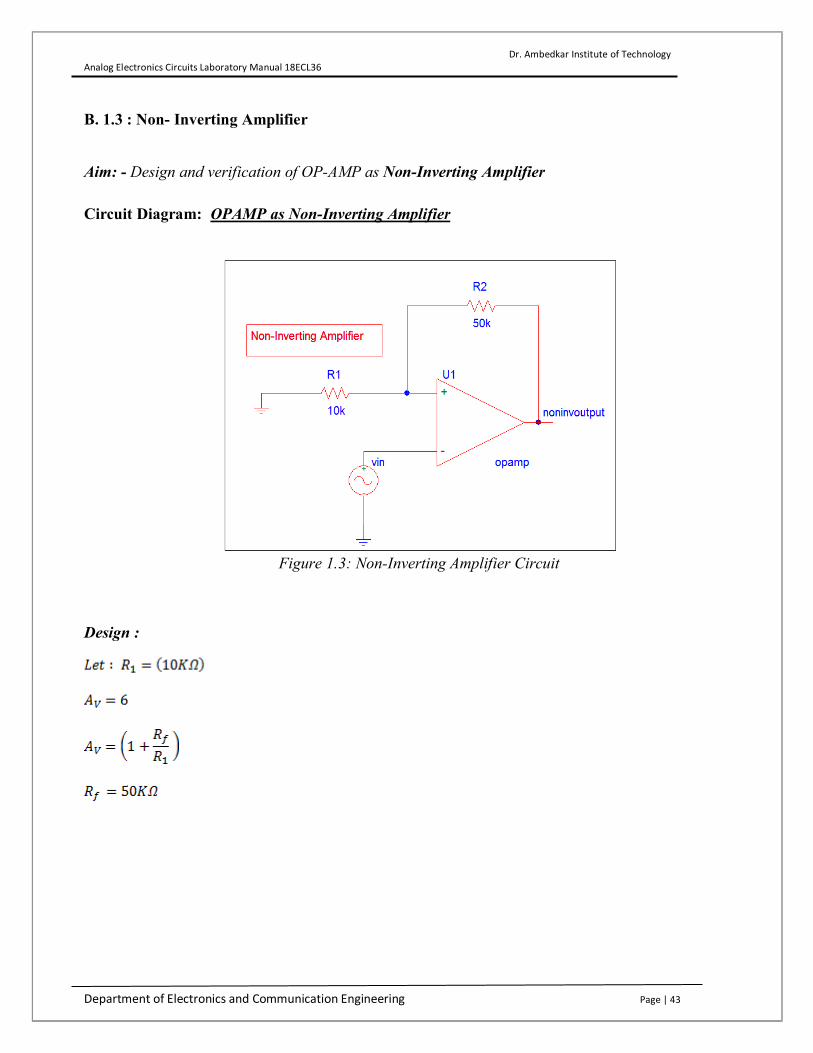
B. 1.3 : Non- Inverting Amplifier
Aim: - Design and verification of OP-AMP as Non-Inverting Amplifier
Circuit Diagram: OPAMP as Non-Inverting Amplifier
Figure 1.3: Non-Inverting Amplifier Circuit
Design :

Dr. Ambedkar Institute of Technology Analog Electronics Circuits Laboratory Manual 18ECL36
Department of Electronics and Communication Engineering Page | 44
Steps to build the Circuit Diagram in PSpice simulation:
1. Press Clt+G (Parts Browser Basic) in Part Name type Opamp, and click Place and Close
option in Part Browser Basic, to place Op-amp in the schematic window.
2. Press Clt+G (Parts Browser Basic) to select input sine wave, in the Part Name type vsin , and
click Place and Close option in Part Browser Basic, to place vsin schematic window.
3. Double click on the vsin icon to add the following parameter
(Note: Each time adding the parameter always press, Save Attr ) Name of the input sine wave = Vin a. DC =0
b. AC =0
c. VOFF = 0
d. VAMPL =0.5v
e. FREQ = 1KHz
4. The positive of the sine wave is connected to the non-inverting terminal of op-amp (‘ - sign’
is non-inverting terminal of op-amp) and negative sign to ground, using draw wire option, connect the wires between the positive input terminal and negative ground terminal.
5. Press Clt+G (Parts Browser Basic) to select resistors, in the Part Name type ‘r’ , and click Place and Close option in Part Browser Basic, to place resistors in the schematic window.

Dr. Ambedkar Institute of Technology Analog Electronics Circuits Laboratory Manual 18ECL36
Department of Electronics and Communication Engineering Page | 45
6. Double click on the resistor icon to add the following parameter .
c. R1 = 10K
d. R2= 50K
7. Select Draw wire option from menu bar to connect wire R1 resistors between inverting terminal (‘+ sign’ is inverting terminal of op-amp) & R1 another end to ground, and between R2 resistors and output , the label the output name as noninvoutput.
8. In Transient window, type
9. Print Step = 0
10. Final time = 5 ms

Dr. Ambedkar Institute of Technology Analog Electronics Circuits Laboratory Manual 18ECL36
Department of Electronics and Communication Engineering Page | 46
11. Click on Analysis in the menu bar, select Simulate option, next Click on Trace in the menu bar, select Add Trace. Add Trace Window displays the input and output label used in the circuit diagram.
12. Select the input label as V1(Vin) used in the circuit diagram to obtain the input sine wave
13. Select the output as V(noninvoutput) used in the circuit diagram to obtain the input sine wave.
Dr. Ambedkar Institute of Technology Analog Electronics Circuits Laboratory Manual 18ECL36
Department of Electronics and Communication Engineering Page | 47
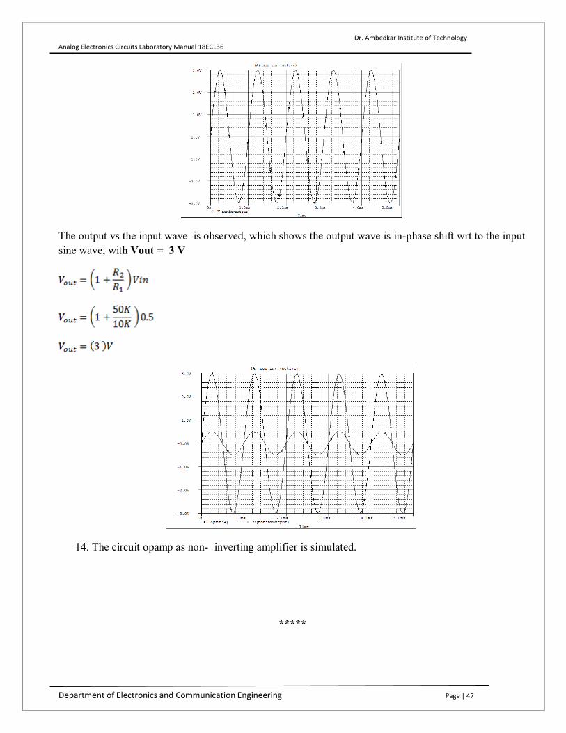
The output vs the input wave is observed, which shows the output wave is in-phase shift wrt to the input sine wave, with Vout = 3 V
14. The circuit opamp as non- inverting amplifier is simulated.
*****

Dr. Ambedkar Institute of Technology Analog Electronics Circuits Laboratory Manual 18ECL36
Department of Electronics and Communication Engineering Page | 48
Experiment No. B.2
Design and verification of Integrator and Differentiator using OP-AMP. B.2.1 Design and verification of Integrator using OP-AMP.
Aim: - Design and Verification of Integrator using OP-AMP
Circuit Diagram: OPAMP as Integrator
Figure 2.1: Integrator Circuit
Design:
Integrator:
Settings:
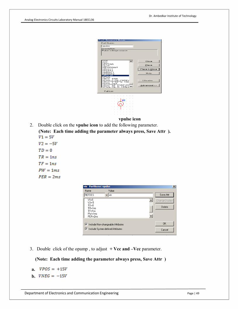
1. Press Clt+G (Parts Browser Basic) to select input square wave, in the Part Name type vpulse , and click Place and Close option in Part Browser Basic, to place vpulse schematic window.
Dr. Ambedkar Institute of Technology Analog Electronics Circuits Laboratory Manual 18ECL36
Department of Electronics and Communication Engineering Page | 49
vpulse icon
2. Double click on the vpulse icon to add the following parameter. (Note: Each time adding the parameter always press, Save Attr ).
3. Double click of the opamp , to adjust + Vcc and –Vcc parameter.
(Note: Each time adding the parameter always press, Save Attr )
a. b.
Dr. Ambedkar Institute of Technology Analog Electronics Circuits Laboratory Manual 18ECL36
Department of Electronics and Communication Engineering Page | 50
c.
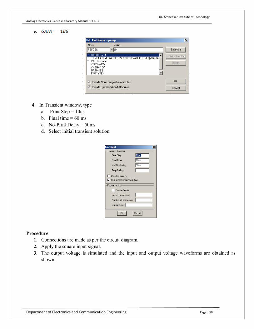
4. In Transient window, type a. Print Step = 10us b. Final time = 60 ms c. No-Print Delay = 50ms d. Select initial transient solution
Procedure
1. Connections are made as per the circuit diagram. 2. Apply the square input signal. 3. The output voltage is simulated and the input and output voltage waveforms are obtained as
shown.

Dr. Ambedkar Institute of Technology Analog Electronics Circuits Laboratory Manual 18ECL36
Department of Electronics and Communication Engineering Page | 51
Figure 2.2: Output waveforms
*****

Dr. Ambedkar Institute of Technology Analog Electronics Circuits Laboratory Manual 18ECL36
Department of Electronics and Communication Engineering Page | 52
B. 2.2 : Design and verification of Differentiator using OP-AMP Aim: - Design and Verification of Differentiator using OP-AMP
Circuit Diagram : OPAMP as Differentiator
Figure 2.1: Differentiator Circuit
Design: Differentiator :
Settings:
1. Press Clt+G (Parts Browser Basic) to select input square wave, in the Part Name type vpulse,
and click Place and Close option in Part Browser Basic, to place vpulse schematic window.

Dr. Ambedkar Institute of Technology Analog Electronics Circuits Laboratory Manual 18ECL36
Department of Electronics and Communication Engineering Page | 53
vpulse icon
2. Double click on the vpulse icon to add the following parameter. (Note: Each time adding the parameter always press, Save Attr ).

Dr. Ambedkar Institute of Technology Analog Electronics Circuits Laboratory Manual 18ECL36
Department of Electronics and Communication Engineering Page | 54
Double click of the opamp , to adjust + Vcc and –Vcc parameter.
(Note: Each time adding the parameter always press, Save Attr )
a. b. c.
3. In Transient window, type a. Print Step = 10us b. Final time = 60 ms c. No-Print Delay = 50ms d. Select initial transient solution
Procedure
1. Connections are made as per the circuit diagram. 2. Apply the square input signal. 3. The output voltage is simulated and the input and output voltage waveforms are obtained as
shown.

Dr. Ambedkar Institute of Technology Analog Electronics Circuits Laboratory Manual 18ECL36
Department of Electronics and Communication Engineering Page | 55
Differentiator circuit Triangular wave to square wave
Figure 2.2: Differentiator Circuit
Figure 2.4: Differentiator triangle to square waveforms
*****

Dr. Ambedkar Institute of Technology Analog Electronics Circuits Laboratory Manual 18ECL36
Department of Electronics and Communication Engineering Page | 56
Experiment No. B.3
Design and Simulation of Function generator to generate square wave and triangular wave generator using OP-AMP.
B. 3.1: Design and Simulation of Function generate triangular wave using OP-AMP Aim: Design and Simulation of Function generate triangular wave using OP-AMP Circuit Diagram: TRIANGULAR WAVE GENERATOR
Figure 3.1: Triangular wave generator Circuit
Design
Settings:
1. Press Clt+G (Parts Browser Basic) to select input square wave, in the Part Name type vpulse , and click Place and Close option in Part Browser Basic, to place vpulse schematic window.

Dr. Ambedkar Institute of Technology Analog Electronics Circuits Laboratory Manual 18ECL36
Department of Electronics and Communication Engineering Page | 57
vpulse icon
2. Double click on the vpulse icon to add the following parameter. (Note: Each time adding the parameter always press, Save Attr ).
3. In Transient window, type
a. Print Step = 10us b. Final time = 60 ms c. No-Print Delay = 50ms d. Select initial transient solution.
4. Double click of the opamp , to adjust + Vcc and –Vcc parameter.
(Note: Each time adding the parameter always press, Save Attr )
a. VPOS = +15V b. VNEG = -15V c. GAIN = 1E6

Dr. Ambedkar Institute of Technology Analog Electronics Circuits Laboratory Manual 18ECL36
Department of Electronics and Communication Engineering Page | 58
Procedure
Connections are made as per the circuit diagram. Apply the square input signal. The output voltage is simulated and the input and output voltage waveforms are obtained
as shown.
Figure 3.2: Output Triangular Waveform
*****

Dr. Ambedkar Institute of Technology Analog Electronics Circuits Laboratory Manual 18ECL36
Department of Electronics and Communication Engineering Page | 59
B. 3.2 : Design and Simulation of Function generate square wave using OP-AMP Aim: Design and Simulation of Function generate square wave using OP-AMP Circuit Diagram: SQUARE WAVE GENERATOR
Figure 3.3: Square Wave Generator Circuit
Design
Settings:
1. Press Clt+G (Parts Browser Basic) to select input triangular wave, in the Part Name type VPWL_ENH , and click Place and Close option in Part Browser Basic, to place vpulse schematic window.

Dr. Ambedkar Institute of Technology Analog Electronics Circuits Laboratory Manual 18ECL36
Department of Electronics and Communication Engineering Page | 60
VPWL_ENH icon
2. Double click on the vpwl_enh icon to add the following parameter.
(Note: Each time adding the parameter always press, Save Attr ).
3. In Transient window, type
a. Print Step = 0ns
b. Final time = 10 ms

Dr. Ambedkar Institute of Technology Analog Electronics Circuits Laboratory Manual 18ECL36
Department of Electronics and Communication Engineering Page | 61
4. Select initial transient solution.
Double click of the opamp , to adjust + Vcc and –Vcc parameter.
(Note: Each time adding the parameter always press, Save Attr )
a. VPOS = +12V
b. VNEG = -12V
c. GAIN = 1E6
Procedure
Connections are made as per the circuit diagram. Apply the triangular input signal. The output voltage is simulated and the input and output voltage waveforms are obtained
as shown.
Figure 3.4: Square Wave Generator Waveform
****

Dr. Ambedkar Institute of Technology Analog Electronics Circuits Laboratory Manual 18ECL36
Department of Electronics and Communication Engineering Page | 62
Experiment No. B.4
Analyze Input, Output characteristics of BJT Common emitter configuration and evaluation of parameters.
Aim: - Analyze Input, Output characteristics of BJT Common emitter configuration and evaluation of parameters.
Circuit Diagram:
Figure 4.1: BJT Common Emitter Circuit
Steps to draw the Circuit Diagram in PSpice simulation: 1. Press Clt+G (Parts Browser Basic) in Part Name type Q2N2222, and click Place and Close
option in Part Browser Basic, to place npn= transistor in the schematic window.
2. To add input DC voltage and bias voltage VCC, follow the below steps:
3. Press Clt+G (Parts Browser Basic) to select dc voltage , in the Part Name type vdc , and click
Place and Close option in Part Browser Basic, to place vdc at the input side and bias voltage in
the schematic window.

Dr. Ambedkar Institute of Technology Analog Electronics Circuits Laboratory Manual 18ECL36
Department of Electronics and Communication Engineering Page | 63
4. Double click on the vdc icon at input side to add the following parameter.
(Note: Each time adding the parameter always press, Save Attr ) Name of the input dc voltage = VBB a. DC =5V
5. Double click on the vdc icon for the bias voltage
Name of the input dc voltage = VBB a. DC =30V
6. Double click on the resistor icon to add the following parameter .
b. R1 = 100K
c. R2= 1K
7. Add label as VBE at input side, and VCE at output side, as shown in circuit diagram to obtain
the characteristic curve
8. Click on Analysis in the menu bar, select Setup option, Select DC Sweep option.
9. In DC Sweep , Select the Voltage source, and type
Name = VBB Start Value : 0 End Value = 5 Increment = 0.5.

Dr. Ambedkar Institute of Technology Analog Electronics Circuits Laboratory Manual 18ECL36
Department of Electronics and Communication Engineering Page | 64
10. In DC Sweep , Select the Nested Sweep
11. In DC Nested Sweep , Select the Voltage source, and enter
Name = VCC Start Value: 0 End Value = 15 Increment = 5 Enable : Enable Nested Sweep.
12. Click on Analysis in the menu bar, select Simulate option, next Click on Plot in the menu
bar, select Axis Setting. In Axis Setting click on Axis variable.

Dr. Ambedkar Institute of Technology Analog Electronics Circuits Laboratory Manual 18ECL36
Department of Electronics and Communication Engineering Page | 65
13. In Axis Variable, disable Alias Names, and Select V(VBE) and Click OK. The X-axis VBE
would be displayed.
14. Next Click on Trace in the menu bar, select Add Trace.
15. Select IB(Q1).

Dr. Ambedkar Institute of Technology Analog Electronics Circuits Laboratory Manual 18ECL36
Department of Electronics and Communication Engineering Page | 66
16. The input characteristics curve (IB vs VBE) is plotted as shown in figure
Figure 4.2: The input characteristics waveform
17. The input characteristics curve (IB vs VBB) is plotted as shown in figure
Figure 4.3: The input characteristics waveform

Dr. Ambedkar Institute of Technology Analog Electronics Circuits Laboratory Manual 18ECL36
Department of Electronics and Communication Engineering Page | 67
To plot output characteristics curve
18. In DC Sweep , Select the Voltage source, and type
a. Name = VCC b. Start Value : 0 c. End Value = 30 d. Increment = 1
19. In DC Sweep , Select the Nested Sweep
20. In DC Nested Sweep , Select the Voltage source, and type
a. Name = VBB b. Start Value: 0 c. End Value = 5 d. Increment =1
Enable : Enable Nested Sweep.

Dr. Ambedkar Institute of Technology Analog Electronics Circuits Laboratory Manual 18ECL36
Department of Electronics and Communication Engineering Page | 68
To plot output characteristics, In simulation select V(VCE) in Axis Variable
21. Next Click on Trace in the menu bar, select Add Trace. Select IC(Q1).
22. The output characteristics curve (IC vs VCE) is plotted as shown in figure
Figure 4.4: Output characteristic waveform

Dr. Ambedkar Institute of Technology Analog Electronics Circuits Laboratory Manual 18ECL36
Department of Electronics and Communication Engineering Page | 69
23. The input characteristics curve (Ic vs VCC) is plotted as shown in figure
Figure 4.5: Output characteristic waveform
Procedure Connections are made as per the circuit diagram. The input and output characteristics curve are obtained as shown.
*****

Dr. Ambedkar Institute of Technology Analog Electronics Circuits Laboratory Manual 18ECL36
Department of Electronics and Communication Engineering Page | 70
Experiment No. B.5
Analyze drain and gate characteristics of JFET Aim: - Analyze drain and gate characteristics of JFET
Circuit Diagram:
Figure 5.1: JFET circuit
Parameter Settings
1. Input values:
Source : Vdc Source: Vdc
Name : Vgs Name: Vds
DC = 0V DC = 20V

Dr. Ambedkar Institute of Technology Analog Electronics Circuits Laboratory Manual 18ECL36
Department of Electronics and Communication Engineering Page | 71
2. DC sweep parameters for drain characteristics
To add values for Vgs, select Nested Sweep, and click on enable nested sweep. Vgs values to be entered in Nested Sweep only
Vds Vgs
Name Vdc Name Vgs
Start values: 0V Start values: 0V
End Value: 20V End Value: 20V
Increment: 1V Increment: 1V
3. To analyze the drain characteristic, plot the graph of Vds vs Idc.
Figure 5.2: Drain characteristics waveform
Dr. Ambedkar Institute of Technology Analog Electronics Circuits Laboratory Manual 18ECL36
Department of Electronics and Communication Engineering Page | 72
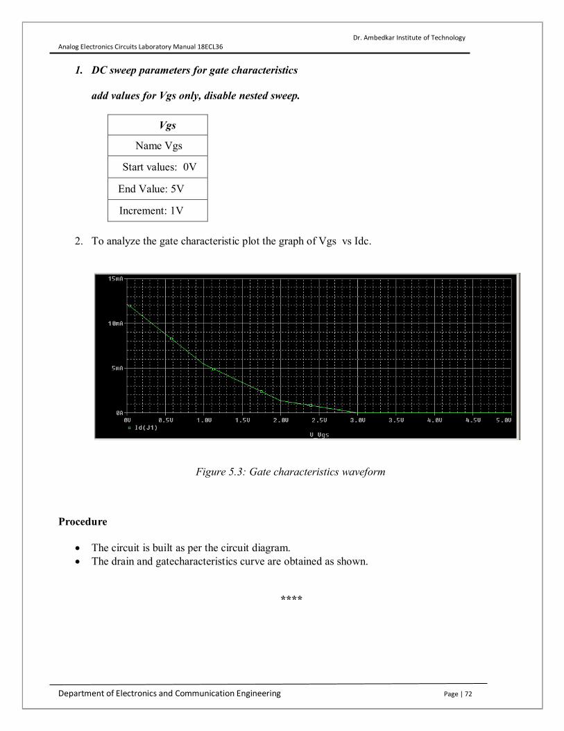
1. DC sweep parameters for gate characteristics add values for Vgs only, disable nested sweep.
Vgs
Name Vgs
Start values: 0V
End Value: 5V
Increment: 1V
2. To analyze the gate characteristic plot the graph of Vgs vs Idc.
Figure 5.3: Gate characteristics waveform
Procedure
The circuit is built as per the circuit diagram. The drain and gatecharacteristics curve are obtained as shown.
****

Dr. Ambedkar Institute of Technology Analog Electronics Circuits Laboratory Manual 18ECL36
Department of Electronics and Communication Engineering Page | 73
Experiment No. B.6
Analyze of Static characteristics of SCR
Aim: - Analyze of Static characteristics of SCR
Circuit Diagram: Silicon Controlled Rectifier (SCR)
Figure 6.1: SCR cirucit
Parameter Settings
1. Input values:
Source : Vdc Source: VSIN
Name : V3 Name: V1
DC = 5V DC = 0
AC=0
VOFF = 0
VAMPL = 12V
FREQ = 50

Dr. Ambedkar Institute of Technology Analog Electronics Circuits Laboratory Manual 18ECL36
Department of Electronics and Communication Engineering Page | 74
2. Input values: R1= 2K R2= 500
3. SCR name : 2N1595.
3. Transient analysis
Print step: 0ns
Final Time: 100ms
4. To analyze the scr characteristic: a. Add Traces: Select I(R2)
Figure 6.2: SCR characteristics waveform
b. Select Plot: Axis Setting: Axis Variable: Select V(X1 : A)

Dr. Ambedkar Institute of Technology Analog Electronics Circuits Laboratory Manual 18ECL36
Department of Electronics and Communication Engineering Page | 75
c. Select Plot: Axis Setting: Axis Variable: Select User Defined: Range -2 to 2.0V
Figure 6.3: Forward characteristics of SCR waveform
Procedure
The circuit is built as per the circuit diagram. The SCR characteristics are obtained as shown.
****