part number: version: date - midas · pdf filespecification part number: version: date: midas...
TRANSCRIPT
SpecificationPart Number:
Version: Date:
Midas Components Limited Electra House 32 Southtown Road Great Yarmouth Norfolk NR31 0DU England
Telephone +44 (0)1493 602602 Fax +44 (0)1493 665111 Email [email protected] Website www.midasdisplays.com

BOOKBINDING AREA
DOC.DATASHEET STATEMENT
The following icons are absolutely designed by Midas independently in 2007-SEP. They are not in commonuse in the LCD industry yet but just used for marking out Midas products’ characteristics quickly andsimply without any special meaning. Midas reserves the composing right and copyright.No one else is allowed to adopt these icons without Midas approval.
1.
The ISO9001 logo used in this document is authorized by SGS (www.sgs.com). Midas had alreadysuccessfully passed the strict and professional ISO9001:2000 Quality Management System Certification andgot the certificate (No.: CN07/00404)
2.
The technologies/techniques/crafts which denoted by the following icons are not exclusively owned by Midas,but also shared by Midas LCD strategic cooperators, however all these technologies/techniques/crafts havebeen finally confirmed by Midas professional engineers and QC department.
3.
SAMPLE APPROVAL document rather than consider this DATASHEET as the standard for judging whether or not theLCD meets your requirements. Once you instruct Midas to a mass-production without definite demand forproviding sample before, Midas will disclaim all responsibility if the mass-production is proved not meeting withyour requirements.
As the difference in test standard and test conditions, also Midas insufficient familiarity with the actual LCDusing environment, all the referred information in this DATASHEET (including the icons) only have two functions:4.1: providing quick reference when you are judging whether or not the product meets your requirements.4.2: listing out definitely the tolerance.
4.
The sequence of the icons is random and doesn’t indicate the importance grade.5.
Icons explanation6.
This icon on the cover indicates the productis with high contrast; Otherwise not.
HIGH CONTRAST LONG LIFE VERSIONThis icon on the cover indicates the productis long life version (over 9K hours guaranteed);Otherwise not.
H C
3.0VVlcm = 3.0V
This icon on the cover indicates the productcan work at 3.0V exactly; otherwise not.
3TIMEs 100% QC EXAMINATIONThis icon on the cover indicates the producthas passed Midas thrice 100% QC.Otherwise not.
This icon on the cover indicates the LED had passedMidas twice strict selection which promises theproduct’s identical color and brightness; Otherwise not.
TWICE SELECTION OF LED MATERIALS
This icon on the cover indicates the productis with high response speed; Otherwise not.
FAST RESPONSE TIME
This icon on the cover indicates the productis with protection circuit; Otherwise not.
PROTECTION CIRCUIT
FFF
Y C
X C
OPERATION TEMPERATURE RANGE
This icon on the cover indicates the operatingtemperature range (X-Y).
This icon on the cover indicates the productmeets ROHS requirements; Otherwise not.
RoHS COMPLIANCE
RoHS
Midas 2006 version logo.Midas is an integrated manufacturer of flatpanel display (FPD). Midas supplies TN, HTN, STN, FSTN monochromeLCD panel; COB, COG, TAB LCD module; and all kinds of LED backlight.
WIDE VIEWING SCOPE
This icon on the cover indicates the productis with wide viewing scope; Otherwise not.
Anti UV VERSION
This icon on the cover indicates the productis against UV line. Otherwise not.
UV
N New structure, new craft, newtechnology and new materials inside both LCDmodule and LCD panel to improve the "RainBow"
N SERIES TECHNOLOGY (2008 developed)

Midas Displays OLED Part Number System
MCO B 21605 A * V - E W I * 1 2 3 4 5 6 7 8 9 10
1 = MCO: Midas Displays OLED
2 = Blank: B: COB (Chip on Board) T: TAB (Taped Automated Bonding)
3 = No of dots: (e.g. 240064 = 240 x 64 dots) (e.g. 21605 = 2 x 16 5mm C.H.)
4 = Series A to Z
5 = Series Variant: A to Z and 1 to 9 – see addendum
6 = Operating Temp Range: A: -30+85° C V: -40+80° C Y: -40 +70° C Z: -30+70° C X: -40 +85° C
7 = Character Set: Blank: Not Applicable E: Multi European Font Set (English/Japanese – Western European (K) – Cyrillic (R))
8 = Colour: Y: Yellow W: White B: Blue R: Red G: Green RGB: Full Colour
9 = Interface: P: Parallel I: I²C S: SPI M: Multi
10 = Voltage Variant: e.g. 3 = 3v
F/Displays/Midas Brand/Midas NEW OLED Part Number System 18 June 2013 2011.doc

Page 3 , Total 62 Pages
Contents 1. Revision History 4
2. General Specification 4
3. Module Coding System 5
4. Interface Pin Function 6
5. Outline Dimension 7
6. Optics & Electrical Characteristics 9
7.. Absolute Maximum Ratings 22
8. Block Diagram 26
9. Timing Characteristics 27
10. Initializing of OLED Module 30
11 Absolute Maximum Ratings 47
12 Electrical Characteristicsical 48
13 Optical Characteristics 48
11. OLED Lifetime 49
12. Reliability 50
13. Inspection specification 52
14 Precautions in use of Modules 58
Page

1. Revision History
DATE VERSION REVISED PAGE NO. Note
2010/08/13
1
First issue
2. General Specification
The Features is described as follow:
Module dimension: 80.0 ×36.0 × 10.0 (max.) mm3
View area: 66.0 × 16.0 mm2
Active area: 56.95 × 11.85 mm2
Number of dots: 16 x 2
Pixel size: 0.55 x 0.65 mm2
Pixel pitch: 0.60 x0.70 mm2
Character size: 2.95x5.55 mm2
Character pitch:3.6 x6.3 mm2
Module type: Character Passive Matrix
Duty: 1/16
Emitting Color: Yellow

4. Interface Pin Function
No. Symbol I/O Function 1 VSS 0V Ground 2 VDD 5.0V Supply Voltage for logic 3 NC - 4 RS H/L H: DATA, L: Instruction code 5 R/W H/L H: Read(MPU→Module) L: Write(MPU→Module) 6 E H,H→L Chip enable signal 7 DB0 H/L Data bit 0 8 DB1 H/L Data bit 1 9 DB2 H/L Data bit 2
10 DB3 H/L Data bit 3 11 DB4 H/L Data bit 4 12 DB5 H/L Data bit 5 13 DB6 H/L Data bit 6 14 DB7 H/L Data bit 7 15 NC - 16 NC -
Brightness Control※※※※
Brightness(nits) Power consumption(measured with random texts) 125(typical) 150mW(5V*30mA)
Notes: 1.When random texts pattern is running , averagely , at any instance , about 1/2 of pixels
will be on.
2. You can to use the display off mode to make long life.
5. Outline Dimension
2.5
31.0
2.5 75.0
66.0(VA)
5.1
161
4.23
11.
85(
AA
)
40.55
80.0 0.5
36.0
0.5
5.7
10.3
18.3
4.957.55
8.0 P2.54*15=38.11.8 16- 1.0PTH 2
10.0Max
1.64- 2.5 PTH4- 5.0 PAD
25.
2
16.0
(VA
)
71.2Vss
RSR/W
NC
DB2
DB0DB1
E
Vdd
9
78
6
2
45
3
1
DB6
DB4DB5
NCNCDB7
13
161514
1112
10 DB3
56.95(AA)
0.650.7
0.65
5.55
0.60.55
2.953.6
6.3
0.75
SCALE 5/1DOT SIZES
The non-specified tolerance of dimension is ±0.3 mm .

IST0010

6. Optics & Electrical Characteristics
REGISTERS IC provides two types of 8-bit registers, namely: Instruction Register (IR) and Data Register (DR). The register is selected using the RS Pin. When the RS pin is set to "0", the Instruction Register Type is selected. When RS pin is set to "1", the Data Register Type is selected. Please refer to the table below.
RS R/WB Operation 0 0 Instruction register write as an internal operation.
0 1 Read busy flag (DB7) and address counter (DB0 to DB6)
1 0 Data register write as an internal operation (DR to DDRAM or CGRAM) 1 1 Data register read as an internal operation (DDRAM or CGRAM to DR)
INSTRUCTION REGISTER (IR) The Instruction Register is used to store the instruction code (i.e. Display Clear, Cursor Home and others), Display Data RAM (DDRAM) Address, and the Character Generator RAM (CGRAM) Address. Instruction register can only be written from the MPU. DATA REGISTER (DR) The Data Register is used as a temporary storage for data that are going to be written into the DDRAM or CGRAM as well as those data that are going to be read from the DDRAM or CGRAM.
BUSY FLAG (BF) The Busy Flag is used to determine whether IC is idle or internally operating. When IC is performing some internal operations, the Busy Flag is set to "1". Under this condition, the no other instruction will not be accepted. When RS Pin is set to "0" and R/WB Pin is set to "1", the Busy Flag will be outputted to the DB7 pin. When IC is idle or has completed its previous internal operation, the Busy Flag is set to "0". The next instruction can now be processed or executed. ADDRESS COUNTER (AC) The address counter is used to assign the Display Data RAM (DDRAM) Address and the Character Generator RAM (CGRAM) Address. When Address information is written into the Instruction Register (IR), this Address information is sent from the Instruction Register to the Address Counter. At the same time, the nature of the Address (either CGRAM or DDRAM) is determined by the instruction. After writing into or reading from the DDRAM or CGRAM, the Address Counter is automatically increased or decreased by 1 (for Write or Read Function). It must be noted that when the RS pin is set to "0" and R/WB is set to "1", the contents of the Address Counter are outputted to the pins -- DB0 to

DB6. DISPLAY DATA RAM (DDRAM) The Display Data RAM (DDRAM) is used to store the Display Data which is represented as 8-bit character code. The Display Data RAM supports an extended capacity of 128 x 8-bits or 128 characters. The Display Data RAM Address (ADD) is set in the Address Counter as a hexadecimal. High Order Bits Low Order Bits
Address Counter (hex) AC6 AC5 AC4 AC3 AC2 AC1 AC0
An example of a DDRAM Address=39 is given below.
DDRAM Address: 39 AC6 AC5 AC4 AC3 AC2 AC1 AC0
0 1 1 1 0 0 1
1-LINE DISPLAY (N=0) When the number of characters displayed is less than 128, the first character is displayed at the head position. The relationship between the DDRAM Address and position on the OLED Panel is shown below. Display Position (digit) 1 2 3 4 …………. 126 127 128
DDRAM address (hexadecimal)
00
01
02
03
………….
7D
7E
7F
For example, when only 8 characters are displayed in one Display Line, the relationship between the DDRAM Address and position on the OLED Panel is shown below. Display Position 1 2 3 4 5 6 7 8
DDRAM address 00 01 02 03 04 05 06 07
Shift left 01 02 03 04 05 06 07 08
Shift right 7F 00 01 02 03 04 05 06

2-LINE DISPLAY (N=1) Case 1: The Number of Characters displayed is less than 64 x 2 lines When the number of characters displayed is less than 64 x 2 lines, then the first character of the first and second lines are displayed starting from the head. It is important to note that every line reserve 64 x8bits DDRAM space. 1st line is 00 to 3F,second line is 40 to 7F.Please refer the figure below. Display Position 1 2 3 4 ………. 61 62 63 64
00 01 02 03 ………. 3C 3D 3E 3F DDRAM Address (hexadecimal) 40 41 42 43 ………. 7C 7D 7E 7F
To illustrate, for 2-line x 20 characters display, the relationship between the DDRAM address and position of the OLED panel is shown below.
Display Position 1 2 3 4 ………. 18 19 20
00 01 02 03 ………. 11 12 13 DDRAM address (hexadecimal) 40 41 42 43 ………. 51 52 53
01 02 03 04 ………. 19 20 21 Shift left 41 42 43 44 ………. 52 53 54
3F 00 01 02 ………. 10 11 12 Shift right
7F 40 41 42 ………. 50 51 52

Case 2: 40-Character x 2 Lines Display IC(Master) can be extended to display 40 characters x 2 lines by cascade the other IC(Slave). When there is a Display Shift operation, the DDRAM Address is also shifted. Please refer to the example below.
SLAVE MODE DATA INPUT When IC is under slave mode, display data is send from the other IC(master).The input data “D” is shifted at the falling edge of CL M/S Mode D CL LAT H Master Output Output Output
L Slave Input Input Input
Display Position
1
2
3
4
5
6
7
8
9
10
11
….
37
38
39
40
00 01 02 03 04 05 06 07 08 09 0A …. 24 25 26 27 40 41 42 43 44 45 46 47 48 49 4A …. 64 65 66 67
DDRAM address
IC display (Master) Cascade 2nd IC(Slave)
01 02 03 04 05 06 07 08 09 0A 0B …. 25 26 27 28
Shift left 41 42 43 44 45 46 47 48 49 4A 4B …. 65 66 67 68
3F 00 01 02 03 04 05 06 07 08 09 …. 23 24 25 26
Shift right 7F 40 41 42 43 44 45 46 47 48 49 …. 63 64 65 66

BIDIRECTIONAL SHIFT REGISTER BLOCK This block shifts the serial data at the falling edge of CL. When SHL is set “H”, the data input from D is shifted from bit100 to bit1 (When IC is “master” mode, D is output; When IC is “slave” mode, D is input). When SHL is set “L”, the data input is shifted from bit1 to bit100. Condition 1 : SHL=”H”
Condition 2 : SHL=”L
CHARACTER GENERATOR ROM (CGROM) The Character Generator ROM (CGROM) is used to generate either 5 x 8 dots or 5 x 10 dots character patterns from 8-bit character codes.IC build in three set of font tables as “Western European”, ”English Japanese” and “English Russian”. User can use software to select suitable font table (Default “English Japanese”) . CHARACTER GENERATOR RAM (CGRAM) The Character Generator RAM (CGRAM) is used to generate either 5 x 8 dot or 5 x 10 dot character patterns. It can generate eight 5 x 8 dot character patterns or four 5 x 10 dot character patterns. The character patterns generated by the CGRAM can be rewritten. User-defined character patterns for the CGRAM are supported.

Page 15 , Total 62 Pages
RELATIONSHIP BETWEEN CGRAM ADDRESS, DDRAM CHARACTER CODE AND CGRAM CHARACTER PATTERNS (FOR 5 X 8 DOT CHARACTER PATTERN) Character Codes Character Patterns (DDRAM Data) CGRAM Address (CGRAM Data)
7 6 5 4 3 2 1 0
5 4 3 2 1 0
7 6 5 4 3 2 1 0 High Low High Low High Low 0 0 0 * * * 1 1 1 1 0 0 0 1 * * * 1 0 0 0 1 0 1 0 * * * 1 0 0 0 1 0 0 0 0 * 0 0 0 0 0 0 0 1 1 * * * 1 1 1 1 0 1 0 0 * * * 1 0 1 0 0 1 0 1 * * * 1 0 0 1 0 1 1 0 * * * 1 0 0 0 1
Character pattern 1
1 1 1 * * * 0 0 0 0 0 Cursor Position 0 0 0 * * * 1 0 0 0 1 0 0 1 * * * 0 1 0 1 0 0 1 0 * * * 1 1 1 1 1 0 0 0 0 * 0 0 1 0 0 1 0 1 1 * * * 0 0 1 0 0 1 0 0 * * * 1 1 1 1 1 1 0 1 * * * 0 0 1 0 0 1 1 0 * * * 0 0 1 0 0
Character pattern 2
1 1 1
* * * 0 0 0 0 0 Cursor position 0 0 0 0 * .
.
.
.
.
.
.
.
.
.
.
.
. . . .
.
.
.
.
.
.
.
.
.
.
.
.
.
.
.
.
.
.
.
.
*
*
*
.
.
.
.
.
.
.
.
.
.
.
.
.
.
.
.
.
.
.
.
Character pattern 3~7
0 0 0 * * * 0 0 0 0 0 0 0 1 * * * 0 1 0 1 0 0 1 0 * * * 0 0 0 0 0 0 0 0 0 * 1 1 1 1 1 1 0 1 1 * * * 0 0 0 0 0 1 0 0 * * * 1 0 0 0 1 1 0 1 * * * 0 1 1 1 0 1 1 0 * * * 0 0 1 0 0
Character pattern 8
1 1 1 * * * 0 0 0 0 0 Cursor position

Notes: 1. * = Not Relevant 2. The character pattern row positions correspond to the CGRAM data bits -- 0 to 4, where bit 4 is in the left position. 3. Character Code Bits 0 to 2 correspond to the CGRAM Address Bits 3 to 5 (3 bits: 8 types) 4. If the CGRAM Data is set to "1", then the selection is displayed. If the CGRAM is set to "0", there no selection is made. 5. The CGRAM Address Bits 0 to 2 are used to define the character pattern line position. The 8th line is the cursor position and its display is formed by the logical OR with the cursor. The 8th line CGRAM data bits 0 to 4 must be set to "0". If any of the 8th line CGRAM data bits 0 to 4 is set to "1", the corresponding display location will light up regardless of the cursor position. 6. When the Character Code Bits 4 to 7 are set to "0", then the CGRAM Character Pattern is selected. It must be noted that Character Code Bit 3 is not relevant and will not have any effect on the character display. Because of this, the first Character Pattern shown above (R) can be displayed when the Character Code is 00H or 08H.

Character Codes Character Patterns (DDRAM Data) CGRAM Address (CGRAM Data)
7 6 5 4 3 2 1 0
5 4 3 2 1 0
7 6 5 4 3 2 1 0 High Low High Low High Low
0 0 0 0 * * * 0 0 1 0 0 0 0 0 1 * * * 0 1 1 1 0 0 0 1 0 * * * 1 0 1 0 1 0 0 1 1 * * * 1 0 1 0 0 0 1 0 0 * * * 0 1 1 0 0 0 1 0 1 * * * 0 0 1 1 0 0 1 1 0 * * * 0 0 1 0 1 0 1 1 1 * * * 1 0 1 0 1 1 0 0 0 * * * 0 1 1 1 0 1 0 0 1 * * * 0 0 1 0 0
Character pattern 1
1 0 1 0 * * * * * * * * Cursor Position 1 0 1 1 * * * * * * * * 1 1 0 0 * * * * * * * * 1 1 0 1 * * * * * * * * 1 1 1 0 * * * * * * * *
0
0
0
0
*
0
0
*
0
0
1 1 1 1 * * * * * * * *
0
0
0
0
*
.
.
.
.
.
.
.
.
*
. . . .
.
.
.
.
.
.
.
.
.
.
.
.
.
.
.
.
.
.
.
.
*
*
*
.
.
.
.
.
.
.
.
.
.
.
.
.
.
.
.
.
.
.
.
Character pattern 2~3
0 0 0 0 * * * 1 0 1 0 1 0 0 0 1 * * * 1 1 1 1 1 0 0 1 0 * * * 1 1 1 1 1 0 0 1 1 * * * 1 1 1 1 1 0 1 0 0 * * * 0 1 1 1 0 0 1 0 1 * * * 0 0 1 0 0 0 1 1 0 * * * 0 0 1 0 0 0 1 1 1 * * * 1 0 1 0 1 1 0 0 0 * * * 0 1 1 1 0 1 0 0 1 * * * 0 0 1 0 0
Character pattern 4
1 0 1 0 * * * * * * * * Cursor Position 1 0 1 1 * * * * * * * * 1 1 0 0 * * * * * * * * 1 1 0 1 * * * * * * * * 1 1 1 0 * * * * * * * *
0
0
0
0
*
1
1
*
1
1
1 1 1 1
* * * * * * * *

Page 18 , Total 62 Pages
Notes: 1. * = Not Relevant 2. The character pattern row positions correspond to the CGRAM data bits -- 0 to 4, where bit 4 is in the left position. 3. Character Code Bits 1 and 2 correspond to the CGRAM Address Bits -- 4 and 5 respectively (2 bits : 4 types) 4. If the CGRAM Data is set to "1", then the selection is displayed. If the CGRAM is set to "0", there no selection is made. 5. The CGRAM Address Bits 0 to 3 are used to define the character pattern line position. The 11th line is the cursor position and its display is formed by the logical OR with the cursor. The 11th line CGRAM data bits 0 to 4 must be set to "0". If any of the 11th line CGRAM data bits 0 to 4 is set to "1", the corresponding display location will light up regardless of the cursor position. 6. When the Character Code Bits 4 to 7 are set to "0", then the CGRAM Character Pattern is selected. It must be noted that Character Code Bit -- 0 and 3 are not relevant and will not have any effect on the character display. Because of this, the Character Pattern shown above ( $ ) can be displayed when the Character Code is 00H, 01H, 08H or 09H.
TIMING GENERATION CIRCUIT The timing signals for the internal circuit operations (i.e. DDRAM, CGRAM, and CGROM) are generated by the Timing Generation Circuit. The timing signals for the MPU internal operation and the RAM Read for Display are generated separately in order to prevent one from interfering with the other. This means that, for example, when the data is being written into the DDRAM, there will be no unwanted interference such as flickering in areas other than the display area. OLED DRIVER CIRCUIT IC provides 16 Common Drivers and 100 Segment Driver Outputs. When a character font and the number of lines to be displayed have been selected, the corresponding Common Drivers output the waveform automatically. A non-selection waveform will be outputted by the rest of the Common outputs. CURSOR/BLINK CONTROL CIRCUIT The cursor or character blinking is generated by the Cursor / Blink Control Circuit. The cursor or the blinking will appear with the digit located at the Display Data RAM (DDRAM) Address Set in the Address Counter (AC). AC6 AC5 AC4 AC3 AC2 AC1 AC0
Address counter 0 0 0 0 1 1 1 CASE 1: FOR 1-LINE DISPLAY

Page 19 , Total 62 Pages
Address Form at DB7 DB6 DB5 DB4 DB3 DB2 DB1 DB0 CA (Character Address ) 1 ADD6 ADD5 ADD4 ADD3 ADD2 ADD1 ADD0
Example: When the Address Counter (AC) is set to 0EH, the cursor position is displayed at DDRAM Address 0EH. Display position 1 2 3 4 5 …… 14 15 …… 19 20 DDRAM address (hexadecimal)
00
01
02
03
04
……
0D
0E
……
12
13
| Cursor Position
Notes: The cursor or blinking appears when the Address Counter (AC) selects the Character Generator RAM (CGRAM). When the AC selects CGRAM Address, then the cursor or the blinking is displayed in a irrelevant and meaningless position. CASE 2: FOR 2-LINE DISPLAY Example: When the Address Counter (AC) is set to 46H, the cursor position is displayed at DDRAM Address 46H. Display position 1 2 3 4 5 6 7 8 …… 19 20
00 01 02 03 04 05 06 07 …… 09 13 DDRAM address (hexadecimal) 40 41 42 43 44 45 46 47 …… 49 53
Cursor Position Notes: The cursor or blinking appears when the Address Counter (AC) selects the Character Generator RAM (CGRAM). When the AC selects CGRAM Address, then the cursor or the blinking is displayed in an irrelevant and meaningless position. CHARACTER MODE ADDRESSING IC provides two kind of character mode. User can fill in 128 characters data (N=0, one line) or 64 characters data per line (N=1, two line) in embedded RAM to display graphic. Character mode address can be controlled by DDRAM address ins truction.
1 2 3 4 …… …… 125 126 127 128
CA=
1000
0000
CA=
1000
0001
CA=
1000
0010
CA=
1000
0011
CA=
1111
1100
CA=
1111
1101
CA=
1111
1110
CA=
1111
1111
(2)2-Line condition (N=1)
1 2 3 4 …… …… 61 62 63 64
CA
=100
0000
0
CA
=100
0000
1
CA
=100
0001
0
CA
=100
0001
1
CA
=101
1110
0
CA
=101
1110
1
CA
=101
1111
0
CA
=101
1111
1
CA=
1100
0000
CA=
1100
0001
CA=
1100
0010
CA=
1100
0011
CA=
1111
1100
CA=
1111
1101
CA=
1111
1110
CA=
1111
1111

Page 21 , Total 62 Pages
GRAPHIC MODE ADDRESSING IC provides not only character mode but also graphic mode. User can fill in 100x16 data in embedded RAM to display graphic. Graphic mode addressing is different from character m ode. Use DDRAM address instruction to set X-axis address of Graphic mode and CGRAM address ins truction to set Y-axis of Graphic m ode. Address Form at DB7 DB6 DB5 DB4 DB3 DB2 DB1 DB0
GXA (Graphic X-axis Address) 1 ADD6 ADD5 ADD4 ADD3 ADD2 ADD1 ADD0 GYA (Graphic Y-axis Address) 0 1 0 0 0 0 0 CGA0
1 2 3 4 …… …… 97 98 99 100 D0 D1 D2 D3 D4 D5 D6
CG
A0=
0
GXA
=100
0000
0 G
YA=0
1000
000
GXA
=100
0000
1 G
YA=0
1000
000
GXA
=100
0001
0 G
YA=0
1000
000
GXA
=100
0001
1 G
YA=0
1000
000
D7 GXA
=111
0000
0 G
YA=0
1000
000
GXA
=111
0000
1 G
YA=0
1000
000
GXA
=111
0001
0 G
YA=0
1000
000
GXA
=111
0001
1 G
YA=0
1000
000
C G X A G X A G X A G X A D0 G X A G X A G X A G X A

Page 22 , Total 62 Pages
7. Absolute Maximum Ratings CHARACTER GENERATOR ROM (CGROM) IC provides three set of character font. Character font can be selected by programming FT. ENGLISH_JAPANESE CHARACTER FONT TABLE(default FT[1 :0]= 00)

Page 23 , Total 62 Pages
WESTERN EUROPEAN CHARACTER FONT TABLE I (FT[1 :0]=01)
Page 24 , Total 62 Pages
ENGLISH_RUSSIAN CHARACTER FONT TABLE(FT[1 :0]=10)

Page 25 , Total 62 Pages
WESTERN EUROPEAN CHARACTER FONT TABLE II (FT[1:0]=1

Page 26 , Total 62 Pages
8. Block Diagram Code
Instruction
RS R/WB DB7 DB6 DB5 DB4 DB3 DB2 DB1 DB0
Description
Max. Execution Time when fsp or fosc = 250KHz
Clea r Displa y
0
0
0
0
0
0
0
0
0
1
Clea rs e ntire di spla y. Set s DD RA M A dd re ss 0 into th e Add re ss Co unt er
6.2m s
Ret urn H om e
0
0
0
0
0
0
0
0
1
0
Set s DD RA M A dd re ss 0 into th e Add re ss Co unt er. Ret urn s shift ed displa y t o origin al po siti on. D DR AM co nte nt s re main un chan ge d. (D B0 i s t e st pi n. U se r sh ould se t D B0 =0 all the time )
0
Entry M ode Set
0
0
0
0
0
0
0
1
I/D
S
Set s cu rso r mo ve di re ctio n a nd sp e cifie s di spl a y shift. (The se o pe ratio n s a re per fo rm ed du ring dat a writ e a nd rea d. )
0
Displa y ON/ OFF Con trol
0
0
0
0
0
0
1
D
C
B
Set s e ntire Di spla y (D ) ON/ OFF. Set s Cu rso r (C ) ON/ OFF. Set s Blin kin g (B) of C ursor Po sition Ch ara cte r.
0
S/C
R/L
0
0
Cu rso r/ Displa y S hift/ Mode/ Pwr
0
0
0
0
0
1
G/ C P WR
1
1
Mo ve s cursor & shift s di spl ay witho ut chan ging D D RAM co nte nt s. Set s Gra phi c/ Cha ra cte r M ode Set s int ernal p o we r o n/of f
0
Fu n ction Set
0
0
0
0
1
DL
N
F
FT1
FT0
Set s int er fa ce da ta le ngt h (D L). Set s nu mb er of di spla y line s (N) . Set s Ch aracte r Fo nt (F ). Set s Fo nt Ta ble (FT)
0
et C GRAM Add re ss
0
0
0
1
AC G
AC G
AC G
AC G
AC G
AC G
Set s C GRAM Ad dre ss. C GRAM data is sent an d re cei ved afte r t hisse tting.
0
et DD RA M Add re ss
0
0
1
AD D
AD D
AD D
AD D
AD D
AD D
AD D
Set s DD RA M A dd re ss. The DD RA M dat a I s se nt and re cei ve d a fte r t his settin g.
0
ea d B u sy Flag & Add re ss
0
1
BF
AC
AC
AC
AC
AC
AC
AC
Rea d s Bu sy Fla g (B F) in dicatin g that i nte rn al op eration is bei ng per fo rm ed. Rea d s A dd re ss Co unt er co nte nt s.
0
Write da ta into t he C GRAM o r DD RA M
1
0
Write D ata
Write s dat a into the C GRA M o r DD RA M
0
Rea d Dat a fro m t he C GRAM o r DD RA M
1
1
Rea d Dat a
Rea d d ata from t he C GRA M o r DD RA M
0

Page 27 , Total 62 Pages
9.Timing Characteristics
AC CHARACTERISTICS Read / Write Characteristics (8080-series MPU) Figure 1. Read / Write Characteristics (8080-series MPU) VDD = 4.7 to 5.3V, Ta = 25 ) Item Signal Symbol Min. Typ. Max. Unit Remark Address setup time Address hold time RS tAS80
tAH80 20 0 - - ns
System cycle time tCY80 500 - - ns
Pulse width (WRB) RW_WRB tPW80(W) 250 - - ns
Pulse width (RDB) E_RDB tPW80(R) 250 - - ns Data setup time Data hold time
tDS80 tDH80
40 20 - - ns
Read access time Output disable time
DB7 to DB0 tACC80
tOD80 - 10 - 180
- ns CL = 100pF
tAS80 tAH80
tCY80
tPW80(R) tPW80(W)
tDH80 tDS80
tACC80 tOD80
0.1VDD 0.9VDD
RS
CSB
DB0 to DB7
RDB, WRB
DB0 to DB7

Page 28 , Total 62 Pages
Read / Write Characteristics (6800-series Microprocessor)
Figure 2. Read / Write Characteristics (6800-series MPU) (VDD = 4.7 to 5.3V, Ta = 25)
Item Signal Symbol Min. Typ. Max. Unit Remark
Address setup time Address hold time RS tAS68
tAH68 20 0 - - ns
System cycle time tCY68 500 - - ns
Pulse width (E) E_RDB tPW68(W) 250 - - ns
Pulse width (E) E_RDB tPW68(R) 250 - - ns Data setup time Data hold time
tDS68 tDH68
40 20 - - ns
Read access time Output disable time
DB7 to DB0 tACC68
tOD68 - 10 - 180
- ns CL = 100pF
tAS68 tAH68
tCY68
tPW68(R) tPW68(W)
tDH68 tDS68
tACC68 tOD68
0.1VDD 0.9VDD
RS
CSB
DB0 to DB7
E
DB0 to DB7

Page 29 , Total 62 Pages
Serial Interface Characteristics
Figure 3. Serial Interface Characteristics (VDD = 4.7 to 5.3V, Ta = 25 ) Item Signal Symbol Min. Typ. Max. Unit Remark Serial clock cycle SCL high pulse widthSCL low pulse width
DB5 (SCL)
tCYS tWHS tWLS
300 100 100
- - -
- - -
ns
CSB setup time CSB hold time CSB tCSS
tCHS 150 150
- -
- - ns
Data setup time Data hold time
DB7 (SDI)
tDSS tDHS
100 100
- -
- - ns
Read access time DB6 (SDO) tACCS - - 80 ns
Serial Interface Characteristics
tCSS
tWHS
tCYS
tDSS tDHS
tCHS
tWLS 0.1VDD 0.9VDD
CSB
DB7 (SDI)
DB5 (SCL)
DB6 (SDO)
TACCS

Page 30 , Total 62 Pages
10.Initializing of OLED Module
(1)8-bit mode

Page 31 , Total 62 Pages
(2)4-bit mode
Page 32 , Total 62 Pages
INSTRUCTIONS IC Instruction Register (IR) and Data Register (DR) are the only registers that can be controlled by the MPU. Prior to the commencement of it internal operation, IC temporarily stores the control information to its Instruction Register (IR) and Data Register (DR) in order to easily facilitate interface with various types of MPU. The internal operations of the IC are determined by the signals (RS, R/WB, DB0 to DB7) that are sent from the MPU. These signals are categorized into 4 instructions types, namely: 1, Function Setting Instructions (i.e. Display, Format, Data Length etc.) 2. Internal RAM Address Setting Instructions 3. Data Transfer with Internal RAM Instructions 4. Miscellaneous Function Instructions The generally used instructions are those that execute data transfers with the internal RAM. However, when the internal RAM addresses are auto incremented/decremented by 1 after each Data Write, the program load of the MPU is lightened. The Display Shift Instruction can be executed at the same time as the Display Data Write, thereby minimizing system development time with maximum programming efficiency.
When an instruction is being executed for an internal operation, only the Busy Flag/Address Read Instruction can be performed. The other instructions are not valid. It should be noted that during the execution of an instruction, the Busy Flag is set to "1". The Busy Flag is set to "0" when the instructions are can be accepted and executed. Therefore, the Busy Flag should be checked to make certain that BF = "0" before sending another instruction from the MPU. If not, the time between the first instruction and the next instruction is longer than the time it takes to execute the instruction itself.

Page 33 , Total 62 Pages
Code
Instruction
RS R/WB DB7 DB6 DB5 DB4 DB3 DB2 DB1 DB0
Description
Max. Execution Time when fsp or fosc = 250KHz
Clea r Displa y
0
0
0
0
0
0
0
0
0
1
Clea rs e ntire di spla y. Set s DD RA M A dd re ss 0 into th e Add re ss Co unt er
6.2m s
Ret urn H om e
0
0
0
0
0
0
0
0
1
0
Set s DD RA M A dd re ss 0 into th e Add re ss Co unt er. Ret urn s shift ed displa y t o origin al po siti on. D DR AM co nte nt s re main un chan ge d. (D B0 i s t e st pi n. U se r sh ould se t D B0 =0 all the time )
0
Entry M ode Set
0
0
0
0
0
0
0
1
I/D
S
Set s cu rso r mo ve di re ctio n a nd sp e cifie s di spl a y shift. (The se o pe ratio n s a re per fo rm ed du ring dat a writ e a nd rea d. )
0
Displa y ON/ OFF Con trol
0
0
0
0
0
0
1
D
C
B
Set s e ntire Di spla y (D ) ON/ OFF. Set s Cu rso r (C ) ON/ OFF. Set s Blin kin g (B) of C ursor Po sition Ch ara cte r.
0
S/C
R/L
0
0
Cu rso r/ Displa y S hift/ Mode/ Pwr
0
0
0
0
0
1
G/ C P WR
1
1
Mo ve s cursor & shift s di spl ay witho ut chan ging D D RAM co nte nt s. Set s Gra phi c/ Cha ra cte r M ode Set s int ernal p o we r o n/of f
0
Fu n ction Set
0
0
0
0
1
DL
N
F
FT1
FT0
Set s int er fa ce da ta le ngt h (D L). Set s nu mb er of di spla y line s (N) . Set s Ch aracte r Fo nt (F ). Set s Fo nt Ta ble (FT)
0
et C GRAM Add re ss
0
0
0
1
AC G
AC G
AC G
AC G
AC G
AC G
Set s C GR AM Add re ss. C GRA Mdata is sen t a nd re ceived aft er thi sse tting.
0
et DD RA M Add re ss
0
0
1
AD D
AD D
AD D
AD D
AD D
AD D
AD D
Set s D D RA M Add re ss. The DD RA M dat a I s sent a nd re cei ve d a fte r t his settin g.
0
ea d B u sy Flag & Add re ss
0
1
BF
AC
AC
AC
AC
AC
AC
AC
Rea d s Bu sy Fla g (B F) in dicatin g that i nte rn al op eration is bei ng per fo rm ed. Rea d s A dd re ss Co unt er co nte nt s.
0
Write dat a into th e C GRAM o r DD RA M
1
0
Write D ata
Write s dat a into the C GRA M o r DD RA M
0
Rea d D ata fro m th e C GRAM o r DD RA M
1
1
Rea d Dat a
Rea d d ata from t he C GRA M o r DD RA M
0
Notes:

Page 34 , Total 62 Pages
1. After the CGRAM/DDRAM Read or Write Instruction has been executed, the RAM Address Counter is incremented or decremented by 1. After the Busy Flag is turned OFF, the RAM Address is updated. 2. I/D=Increment/Decrement Bit - I/D="1": Increment - I/D="0": Decrement 3. S=Shift Entire Display Control Bit. When S=”0”, shift function disable. 4. BF=Busy Flag - BF="1": Internal Operating in Progress - BF="0": No Internal Operation is being executed, next instruction can be accepted. 5. R/L=Shift Right/Left - R/L="1": Shift to the Right - R/L="0": Shift to the Left 6. S/C=Display Shift/Cursor Move - S/C="1": Display Shift - S/C="0": Cursor Move 7. G/C=Graphic/Character mode selection. G/C=”0”, Character mode is selected. G/C=”1”, Graphic
mode is selected. 8. PWR=Internal DCDC on/of control. PWR=”1”, DCDC on. PWR=”0”, DCDC off. 9. DDRAM=Display Data RAM 10. CGRAM=Character Generator RAM 11. ACG=CGRAM Address 12. ADD=Address Counter Address (corresponds to cursor address) 13. AC=Address Counter (used for DDRAM and CGRAM Addresses) 14. F=Character Pattern Mode - F="1": 5 x 10 dots - F="0": 5 x 8 dots 15. N=Number of Lines Displayed - N="1": 2 -Line Display - N="0": 1-Line Display
INSTRUCTION DESCRIPTION

Page 35 , Total 62 Pages
CLEAR DISPLAY INSTRUCTION RS R/WB DB7 DB6 DB5 DB4 DB3 DB2 DB1 DB0 0 0 0 0 0 0 0 0 0 1
This instruction is used to clear the Display Write Space 20H in all DDRAM Addresses. That is, the character pattern for the Character Code 20H must be a BLANK pattern. It then sets the DDRAM Address 0 into the Address Counter and reverts the display to its original state (if the display has been shifted). The display will be cleared and the cursor or blinking will go to the left edge of the display. If there are 2 lines displayed, the cursor or blinking will go to the first line 's left edge of the display. Under the Entry Mode, this instruction also sets the I/D to 1 (Increment Mode). The S Bit of the Entry Mode does not change. RETURN HOME INSTRUCTION RS R/WB DB7 DB6 DB5 DB4 DB3 DB2 DB1 DB0 0 0 0 0 0 0 0 0 1 *
Note: * = Not Relevant This instruction is used to set the DDRAM Address 0 into the Address Counter and revert the display to its original status (if the display has been shifted). The DDRAM contents do not change.The cursor or blinking will go to the left edge of the display. If there are 2 lines displayed, the cursor or blinking will go to the first line's left edge of the display.

Page 36 , Total 62 Pages
ENTRY MODE SET INSTRUCTION The Entry Mode Set Instruction has two controlling bits: I/D and S. Please refer to the table below. RS R/WB DB7 DB6 DB5 DB4 DB3 DB2 DB1 DB0 0 0 0 0 0 0 0 1 I/D S
I/D IS THE INCREMENT/DECREMENT BIT. When I/D is set to "1", the DDRAM Address is incremented by "1" when a character code is written into or read from the DDRAM. An increment of 1 will move the cursor or blinking one step to the right. When I/D is set to "0", the DDRAM is decremented by 1 when a character code is written into or read from the DDRAM. A decrement of 1 will move the cursor or blinking one step to the left. S: SHIFT ENTIRE DISPLAY CONTROL BIT This bit is used to shift the entire display. When S is set to "1", the entire display is shifted to the right (when I/D ="0") or left (when I/D ="1"). When S is set to "0", the display is not shifted. Ex1 : I/D=1, S=1
Ex2 : I/D=0, S=1
DISPLAY ON/OFF CONTROL INSTRUCTION The Display On / OFF Instruction is used to turn the display ON or OFF. The controlling bits are D, C and B. RS R/WB DB7 DB6 DB5 DB4 DB3 DB2 DB1 DB0

Page 37 , Total 62 Pages
0 0 0 0 0 0 1 D C B CURSOR/DISPLAY SHIFT INSTRUCTION This instruction is used to shift the cursor or display position to the left or right without writing or reading the Display Data. This function is used to correct or search the display. Please refer to the table below. RS R/WB DB7 DB6 DB5 DB4 DB3 DB2 DB1 DB0 0 0 0 0 0 1 S/C R/L 0 0 0 0 0 0 0 1 G/C PW
R1 1
S/C R/L Shift Function 0 0 Shifts the cursor position to the left. (AC is decremented by 1). 0 1 Shifts cursor position to the right. (AC incremented by 1). 1 0 Shifts entire display to the left. The cursor follows the display shift. 1 1 Shifts the entire display to the right. The cursor follows the display shift.
In a 2-line Display, the cursor moves to the second line when it passes the 40th digit of the first line. The first and second line displays will shift at the same time. When the displayed data is shifted repeatedly, each line moves only horizontally. The second line display does not shift into the first line position. The Address Counter (AC) contents will not change if the only action performed is a Display Shift. G/C: GRAPHIC MODE / CHARACTER MODE SELECTION This bit is used to select the display mode for further process. When G/C = 1, the GRAPHIC MODE will be selected. When G/C = 0, the CHARACTER MODE will be selected. PWR: ENABLE/DISABLE INTERNAL POWER This bit is used to turn ON or turn OFF the internal power. When PWR = 1, the internal power is turned ON. When PWR = 0, the internal power is turned OFF. FUNCTION SET INSTRUCTION The Function Set Instruction has three controlling 3 bits, namely: DL, N and F. Please refer to the table below. RS R/WB DB7 DB6 DB5 DB4 DB3 DB2 DB1 DB0

Page 38 , Total 62 Pages
DL: INTERFACE DATA LENGTH CONTROL BIT This is used to set the interface data length. When DL is set to "1", the data is sent or received in 8-bit length via the DB0 to DB7 (for an 8-Bit Data Transfer). When DL is set to "0", the data is sent or received in 4-bit length via DB4 to DB7 (for a 4-Bit Data Transfer). When the 4-bit data length is selected, the data must be sent or received twice. N: NUMBER OF DISPLAY LINE This is used to set the number of display lines. When N="1", the 2-line display is selected. When N is set to "0", the 1-line display is selected. F: CHARACTER FONT SET This is used to set the character font set. When F is set to "0", the 5 x 8 dot character font is selected. When F is set to "1", the 5 x 10 dot character font is selected. It must be noted that the character font setting must be performed at the head of the program before executing any instructions other than the Busy Flag and Address Instruction. Otherwise, the Function Set Instruction cannot be executed unless the interface data length is changed. FT1, FT0: FONT TABLE SELECTION These two bits are used to select one font table out of the three for further process. When (FT1, FT0) = (0, 0), the ENGLISH_JAPANESE CHARACTER FONT TABLE will be selected.
(FT1, FT0) = (0, 1), the WESTERN EUROPEAN CHARACTER FONT TABLE will be selected.
(FT1, FT0) = (1, 0), the ENGLISH_RUSSIAN CHARACTER FONT TABLE will be selected. (FT1, FT0) = (1, 1), N/A Note: The default setting for FT1 and FT0 is 0 and 0 respectively which means the default Font Table is ENGLISH_JAPANESE CHARACTER FONT TABLE. SET CGRAM ADDRESS INSTRUCTION This instruction is used to set the CGRAM Address binary AAAAAA into the Address Counter. Data is then written to or read from the MPU for CGRAM.
RS R/WB DB7 DB6 DB5 DB4 DB3 DB2 DB1 DB0 0 0 0 0 ACG ACG ACG ACG ACG ACG Note: ACG is the CGRAM Addres SET DDRAM ADDRESS INSTRUCTION This instruction is used to set the DDRAM Address binary AAAAAAA into the Address Counter.
FT0 FT1 F N DL 1 0 0 0 0

Page 39 , Total 62 Pages
The data is written to or read from the MPU for the DDRAM. If 1-line display is selected (N="0"), then AAAAAAA can be 00H to 4FH. When the 2-line display is selected, then AAAAAAA can be 00H to 27H for the first line and 40H to 67H for the second line. RS R/WB DB7 DB6 DB5 DB4 DB3 DB2 DB1 DB0 0 0 1 ADD ADD ADD ADD ADD ADD ADD
Note: ADD = DDRAM Address READ BUSY FLAG AND ADDRESS INSTRUCTION This instruction is used to read the Busy Flag (BF) to indicate if IC is internally operating on a previously received instruction. If BF is set to "1", then the internal operation is in progress and the next instruction will not be accepted. If the BF is set to "0", then the previously received instruction has been executed and the next instruction can be accepted and processed. It is important to check the BF status before proceeding to the next write operation. The value of the Address Counter in binary AAAAAAA is simultaneously read out. This Address Counter is used by both the CGRAM and the DDRAM and its value is determined by the previous instruction. The contents of the address are the same as for the instructions -- Set CGRAM Address and Set DDRAM Address.
RS R/WB DB7 DB6 DB5 DB4 DB3 DB2 DB1 DB0 0 1 BF AC AC AC AC AC AC AC Notes: 1. BF=Busy Flag 2. AC=Address Counter
WRITE DATA TO CGRAM / DDRAM INSTRUCTION This instruction writes 8-bit binary data -- DDDDDDDD to the CGRAM or the DDRAM. The previous CGRAM or DDRAM Address setting determines whether a data is to be written into the CGRAM or the DDRAM. After the write process is completed, the address is automatically incremented or

Page 40 , Total 62 Pages
decremented by 1 in accordance with the Entry Mode instruction. It must be noted that the Entry Mode instruction also determines the Display Shift. RS R/WB DB7 DB6 DB5 DB4 DB3 DB2 DB1 DB0 1 0 D D D D D D D D
READ DATA FROM THE CGRAM OR DDRAM INSTRUCTION This instruction reads the 8-bit binary data -- DDDDDDDD from the CGRAM or the DDRAM. The Set CGRAM Address or Set DDRAM Address Set Instruction must be executed before this instruction can be performed, otherwise, the first Read Data will not be valid. RS R/WB DB7 DB6 DB5 DB4 DB3 DB2 DB1 DB0 1 1 D D D D D D D D
MPU INTERFACE IC provides High-speed 8-bit parallel bi-directional interface with 6800-series or 8080-series and serial interface. User can choice by signal “PS” and “C68”. 68 – series interface (a) 8-BIT mode(Not available for serial mode) When IC interfaces with an 8-bit MPU, DB0 to DB7 are used. The 8-bit data transfer starts from the four high order bits --DB4 to DB7 followed by the four low order bits -- DB0 to DB3.An example of a Busy Flag Check Timing in an 8-Bit MPU Interface is given in the diagra
(b) 4-BIT mode (Not available for serial mode) IC can be configured to interface with a 4-bit MPU and is selected via a program. If the I/O port of the 4-Bit MPU from which IC is connected to, is capable of transferring 8 bits, then an 8-bit data transfer operation is executed. Otherwise, two 4-bit data transfer operations are needed to

Page 41 , Total 62 Pages
satisfy one complete data transfeUnder the 4-bit data transfer, DB4 to DB7 are used as bus lines. DB0 to DB3 are disabled. The data transfer between IC and MPU is completed after two 4-bit data have been transferred. The Busy Flag must be checked (one instruction) after completion of the data transfer (that is, 4-bit data has been transferred twice.). The Busy Flag must be checked after two 4-bits data transfer has been completed. Please refer to the diagram below for a 4-bit data transfer timing sequence.
where: 1. IR7=Instruction Bit 7 2. IR3=Instruction Bit 3 3. AC3=Address Counter 3
From the above timing diagram, it is important to note that the Busy Flag Check and the data
transfer are both executed twice.
80 – series interface (a) 8-BIT mode

Page 42 , Total 62 Pages
(b) 4-BIT mode
Serial interface 3-Line series Write/Read

Page 43 , Total 62 Pages
AC CHARACTERISTICS Read / Write Characteristics (8080-series MPU)
tAS80 tAH80
tCY80
tPW80(R) tPW80(W)
tDH80 tDS80
tACC80 tOD80
0.1VDD 0.9VDD
RS
CSB
DB0 to DB7
RDB, WRB
DB0 to DB7

Page 44 , Total 62 Pages
Figure 1. Read / Write Characteristics (8080-series MPU) VDD = 4.7 to 5.3V, Ta = -40 to +85 ) Item Signal Symbol Min. Typ. Max. Unit Remark Address setup time Address hold time RS tAS80
tAH80 0 0 - - ns
System cycle time tCY80 300 - - ns
Pulse width (WRB) RW_WRB tPW80(W) 80 - - ns
Pulse width (RDB) E_RDB tPW80(R) 80 - - ns Data setup time Data hold time
tDS80 tDH80
40 15 - - ns
Read access time Output disable time
DB7 to DB0 tACC80
tOD80 - 10 - 140
100 ns CL = 100pF
Read / Write Characteristics (6800-series Microprocessor) Figure 2. Read / Write Characteristics (6800-series MPU)
tAS68 tAH68
tCY68
tPW68(R) tPW68(W)
tDH68 tDS68
tACC68 tOD68
0.1VDD 0.9VDD
RS
CSB
DB0 to DB7
E
DB0 to DB7

Page 45 , Total 62 Pages
(VDD = 4.7 to 5.3V, Ta = -40 to +85 ) Item Signal Symbol Min. Typ. Max. Unit Remark Address setup time Address hold time RS tAS68
tAH68 0 0 - - ns
System cycle time tCY68 300 - - ns
Pulse width (E) E_RDB tPW68(W) 80 - - ns
Pulse width (E) E_RDB tPW68(R) 80 - - ns Data setup time Data hold time
tDS68 tDH68
40 0 - - ns
Read access time Output disable time
DB7 to DB0 tACC68
tOD68 - 5 - 70
50 ns CL = 100pF
Serial Interface Characteristics Figure 3. Serial Interface Characteristics (VDD = 4.7 to 5.3V, Ta = -40 to +85 ) Item Signal Symbol Min. Typ. Max. Unit Remark
tCSS
tWHS
tCYS
tDSS tDHS
tCHS
tWLS 0.1VDD 0.9VDD
CSB
DB7 (SDI)
DB5 (SCL)
DB6 (SDO)
TACCS

Page 46 , Total 62 Pages
Serial clock cycle SCL high pulse width SCL low pulse width
DB5 (SCL)
tCYS tWHS tWLS
250 100 100
- - -
- - -
ns
CS1B setup time CS1B hold time CSB tCSS
tCHS 150 150
- -
- - ns
Data setup time Data hold time
DB7 (SDI)
tDSS tDHS
100 100
- -
- - ns
Read access time DB6 (SDO) tACCS - - 50 ns

Page 47 , Total 62 Pages
11. Absolute Maximum Ratings
Item Symbol Min Max Unit Notes
Operating Temperature TOP -40 +80
Storage Temperature TST -40 +80
Input Voltage VI -0.3 VDD V Supply Voltage For Logic VDD-VSS -0.3 5.3 V

Page 48 , Total 62 Pages
12. Electrical Characteristicsical
Item Symbol Condition Min Typ Max Unit
Supply Voltage For Logic VDD-VSS - 3.0 5.0 5.3 V
Input High Volt. VIH - 0.9 VDD - VDD V
Input Low Volt. VIL - GND - 0.1VDD V
Output High Volt. VOH IOH=-0.5mA 0.8 VDD - VDD V
Output Low Volt. VOL IOL=0.5mA GND - 0.2 VDD V
Supply Current IDD VDD=5V - 16 - mA
CIEx(Yellow) x,y(CIE1931) 0.44 0.48 0.52 CIEy(Yellow) x,y(CIE1931) 0.46 0.50 0.54
13. Optical Characteristics
Item Symbol Condition Min Typ Max Unit
(V)θ 160 deg View Angle
(H)φ 160 deg
Contrast Ratio CR Dark 2000:1 - -
T rise - 10 µs Response Time
T fall - 10 µs
Supply Voltage For Logic 5V 50% Check Board Brightness
With polarizer 125 nits
Supply Voltage For Logic 3V 50% Check Board Brightness
With polarizer 175 nits
Page 49 , Total 62 Pages
14.OLED Lifetime
ITEM Conditions Typ Remark
Operating Life Time
Ta=25 /Initial 50% CheckBoard brightness 125nits
100,000 Hrs Note
Notes: 1. Simulation pattern for operation test: interchanging with 50% checkboard
The brightness decay does not exceed 50%. 2. You can use the display off mode to make long life. 3.The average operating lifetime at room temperature is estimated by the accelerated operation
at high temperature conditions.

Page 50 , Total 62 Pages
15. Reliability
Content of Reliability Test Environmental Test
Test Item Content of Test Test Condition Applicable Standard
High Temperature storage
Endurance test applying the high storage temperature for a long time.
80 240hrs ——
High Temperature Operation
Endurance test applying the electric stress (Voltage & Current) and the thermal stress to the element for a long time.
80 240hrs ——
Low Temperature Operation
Endurance test applying the electric stress under low temperature for a long time.
-40 240hrs ——
High Temperature/ Humidity Storage
Endurance test applying the high temperature and high humidity storage for a long time.
60 ,90%RH 240hrs ——
Temperature Cycle
Endurance test applying the low and high temperature cycle. -40 25 80 30min 5min 30min 1 cycle
-40 /80 100 cycles ——
Mechanical Test
Vibration test Endurance test applying the vibration during transportation and using.
10~22Hz→1.5mmp-p 22~500Hz→1.5G Total 0.5hrs
——
Shock test Constructional and mechanical endurance test applying the shock during transportation.
50G Half sign wave 11 msedc 3 times of each direction
——
Atmospheric pressure test
Endurance test applying the atmospheric pressure during transportation by air.
115mbar 40hrs ——
Others
Static electricity test
Endurance test applying the electric stress to the terminal.
VS=800V,RS=1.5kΩ CS=100pF 1 time
——
***Supply voltage for logic system=5V. Supply voltage for OLED system =Operating voltage at 25

Page 51 , Total 62 Pages
Test and measurement conditions 1. All measurements shall not be started until the specimens attain to temperature stability.
After the completion of the described reliability test, the samples were left at room temperature for 2 hrs prior to conducting the failure test at 23±5°C; 55±15% RH.
2. All-pixels-on is used as operation test pattern. 3. The degradation of Polarizer are ignored for High Temperature storage, High Temperature/
Humidity Storage, Temperature Cycle Evaluation criteria 1. The function test is OK. 2. No observable defects. 3. Luminance: > 50% of initial value. 4. Current consumption: within ± 50% of initial value. APPENDIX: RESIDUE IMAGE Because the pixels are lighted in different time, the luminance of active pixels may reduce or differ from inactive pixels. Therefore, the residue image will occur. To avoid the residue image, every pixel needs to be lighted up uniformly.
Page 52 , Total 62 Pages
16. Inspection specification NO Item Criterion AQL
01 Electrical Testing
1.1 Missing vertical, horizontal segment, segment contrast defect. 1.2 Missing character, dot or icon. 1.3 Display malfunction. 1.4 No function or no display. 1.5 Current consumption exceeds product specif ications. 1.6 Viewing angle defect. 1.7 Mixed product types. 1.8 Contrast defect.
0.65
02 Black or
bright spots on OLED
(display only)
2.1 Bright and black spots on display ≦0.25mm, no more than three Bright or black spots present.
2.2 Densely spaced: No more than two spots or lines within 3mm
2.5
3.1 Round type : As follow ing drawing
Φ=( x + y ) / 2
SIZE Acceptable Q TY
Φ≦0.10 Accept no dense
0.10<Φ≦0.20 2 0.20<Φ≦0.25 1 0.25<Φ 0
2.5
03
Black spots, bright spots, contaminatio
n (non-display)
3.2 Line type : (As follow ing drawing)
Length Width Acceptable Q TY --- W≦0.02 Accept no dense
L≦3.0 0.02<W≦0.03 L≦2.5 0.03<W≦0.05 2
--- 0.05<W As round type
2.5
04 Polarizer bubbles
If bubbles are visible, judge using black spot specif ications, not easy to f ind, must check in specify direction.
Size Φ Acceptable Q TY Φ≦0.20 Accept no dense
0.20<Φ≦0.50 3 0.50<Φ≦1.00 2 1.00<Φ 0
Total Q TY 3
2.5

Page 53 , Total 62 Pages
NO Item Criterion AQL 05 Scratche
s Follow NO.3 black spots, bright spots, contamination
06 Chipped glass
Symbols Define: x: Chip length y: Chip width z: Chip thickness k: Seal width t: Glass thickness a: OLED side length L: Electrode pad length: 6.1 General glass chip : 6.1.1 Chip on panel surface and crack between panels:
z: Chip
thickness y: Chip width x: Chip length
Z≦1/2t Not over viewing area
x≦1/8a
1/2t<z≦2t Not exceed 1/3k
x≦1/8a
If there are 2 or more chips, x is total length of each chip. 6.1.2 Corner crack:
z: Chip
thickness y: Chip width x: Chip length
Z≦1/2t Not over viewing area
x≦1/8a
1/2t<z≦2t Not exceed 1/3k
x≦1/8a
If there are 2 or more chips, x is the total length of each chip.
2.5
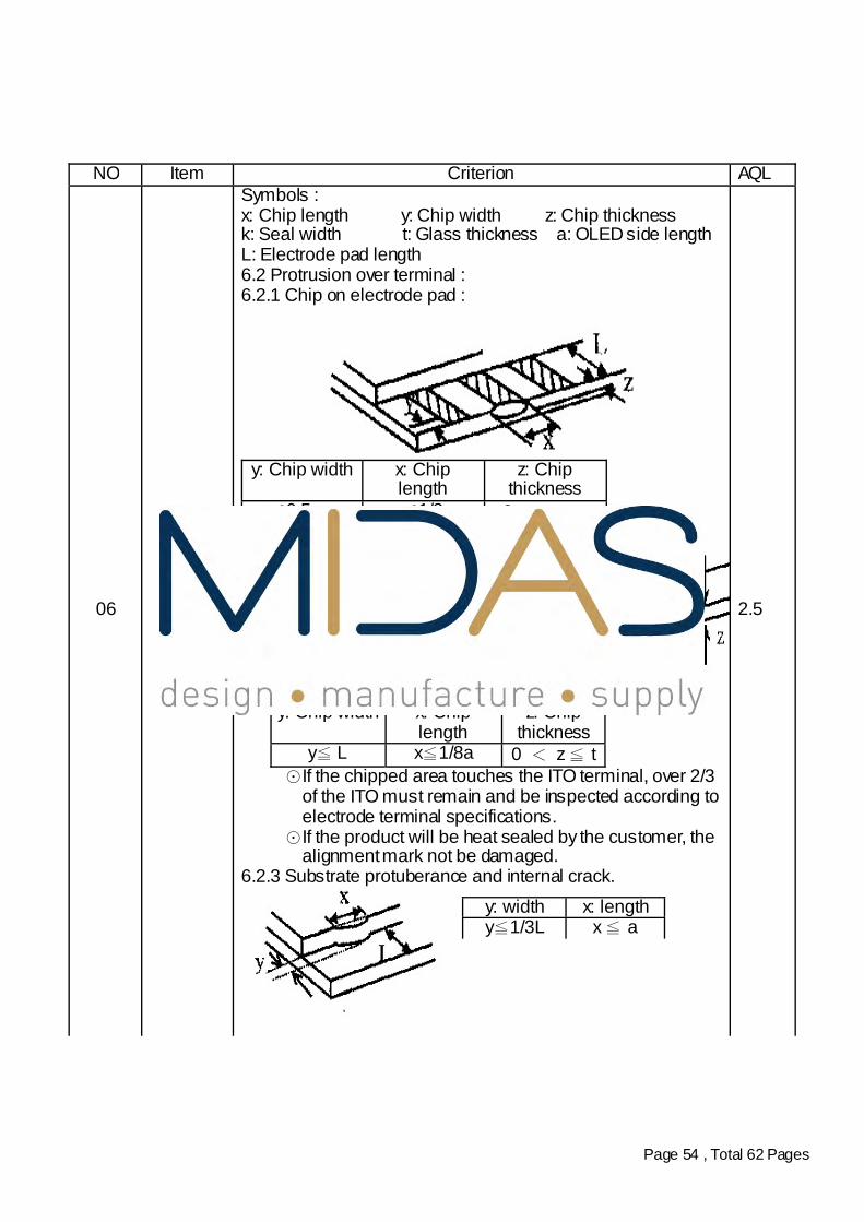
Page 54 , Total 62 Pages
NO Item Criterion AQL
06 Glass crack
Symbols : x: Chip length y: Chip width z: Chip thickness k: Seal width t: Glass thickness a: OLED side length L: Electrode pad length 6.2 Protrusion over terminal : 6.2.1 Chip on electrode pad :
y: Chip width x: Chip
length z: Chip
thickness y≦0.5mm x≦1/8a 0 < z ≦ t
6.2.2 Non-conductive portion:
y: Chip width x: Chip length
z: Chip thickness
y≦ L x≦1/8a 0 < z ≦ t If the chipped area touches the ITO terminal, over 2/3
of the ITO must remain and be inspected according to electrode terminal specifications.
If the product will be heat sealed by the customer, the alignment mark not be damaged.
6.2.3 Substrate protuberance and internal crack.
y: width x: length y≦1/3L x ≦ a
2.5
Page 55 , Total 62 Pages
NO Item Criterion AQL
07 Cracked
glass The OLED with extensive crack is not acceptable. 2.5
08 Bezel 8.1 Bezel may not have rust, be deformed or have
fingerprints, stains or other contamination. 8.2 Bezel must comply with job specifications.
2.5 0.65
9 PCB、
COB
9.1 COB seal may not have pinholes larger than 0.2mm or contamination.
9.2 COB seal surface may not have pinholes through to the IC.
9.3 The height of the COB should not exceed the height indicated in the assembly diagram.
9.4 There may not be more than 2mm of sealant outside the seal area on the PCB. And there should be no more than three places.
9.5 No oxidation or contamination PCB terminals. 9.6 Parts on PCB must be the same as on the production
characteristic chart. There should be no wrong parts, missing parts or excess parts.
9.7 The jumper on the PCB should conform to the product characteristic chart.
9.8 If solder gets on bezel tab pads, zebra pad or screw hold pad, make sure it is smoothed down.
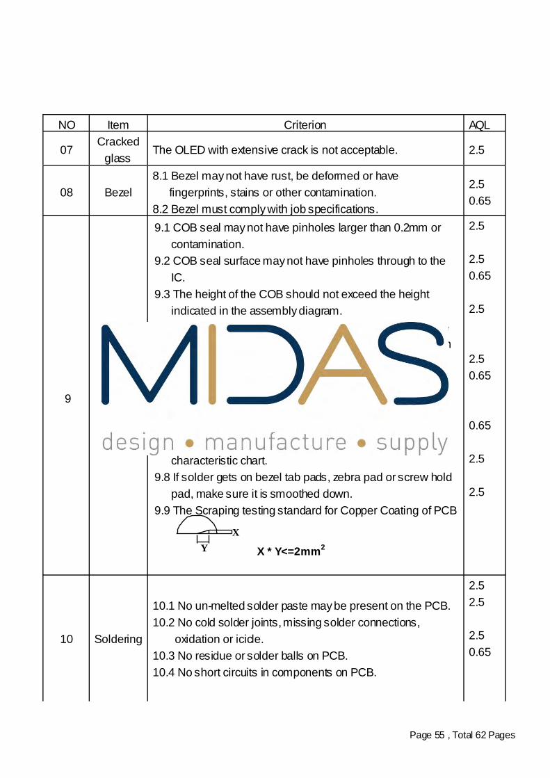
9.9 The Scraping testing standard for Copper Coating of PCB
Y
X
X * Y<=2mm2
2.5 2.5 0.65 2.5 2.5 0.65 0.65 2.5 2.5
10 Soldering
10.1 No un-melted solder paste may be present on the PCB. 10.2 No cold solder joints, missing solder connections,
oxidation or icicle. 10.3 No residue or solder balls on PCB. 10.4 No short circuits in components on PCB.
2.5 2.5 2.5 0.65
Page 56 , Total 62 Pages
NO Item Criterion AQL
11 General appearance
11.1 No oxidation, contamination, curves or, bends on
interface Pin (OLB) of TCP. 11.2 No cracks on interface pin (OLB) of TCP. 11.3 No contamination, solder residue or solder balls on
product. 11.4 The IC on the TCP may not be damaged, circuits. 11.5 The uppermost edge of the protective strip on the
interface pin must be present or look as if it causes the interface pin to sever.
11.6 The residual rosin or tin oil of soldering (component or chip component) is not burned into brown or black color.
11.7 Sealant on top of the ITO circuit has not hardened. 11.8 Pin type must match type in specification sheet. 11.9 OLED pin loose or missing pins. 11.10 Product packaging must the same as specified on
packaging specification sheet. 11.11 Product dimension and structure must conform to
product specification sheet.
2.5 0.65 2.5 2.5 2.5 2.5 2.5 0.65 0.65 0.65 0.65
Page 57 , Total 62 Pages
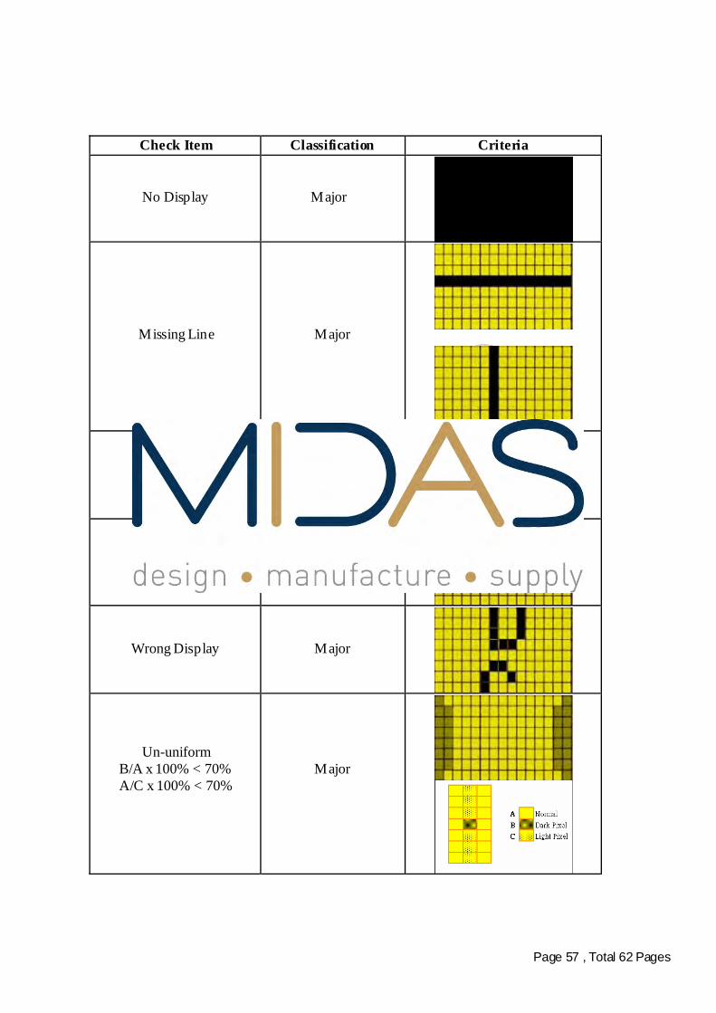
Check Item Classification Criteria
No Display
Major
Missing Line
Major
Pixel Short
Major
Darker Short
Major
Wrong Display
Major
Un-uniform B/A x 100% < 70% A/C x 100% < 70%
Major

Page 58 , Total 62 Pages
17. Precautions in use of Modules
1. Avoid applying excessive shocks to the module or making any alterations or modifications to it.
2. Don’t make extra holes on the printed circuit board, modify its shape or change the components of OLED module.
3. Don’t disassemble the OLED module. 4. Don’t operate it above the absolute maximum rating. 5. Don’t drop, bend or twist OLED module. 6. Soldering: only to the I/O terminals. 7. Storage: please storage in anti-static electricity container and clean environment. 8. Midas have the right to change the passive components (Resistors,capacitors and other passive components will have different appearance and
color caused by the different supplier.) 9. Midas have the right to change the PCB Rev.