pcf2129 accurate rtc with integrated quartz crystal for ... · 1. general description the pcf2129...
TRANSCRIPT

1. General description
The PCF2129 is a CMOS1 Real Time Clock (RTC) and calendar with an integrated Temperature Compensated Crystal (Xtal) Oscillator (TCXO) and a 32.768 kHz quartz crystal optimized for very high accuracy and very low power consumption. The PCF2129 has a selectable I2C-bus or SPI-bus, a backup battery switch-over circuit, a programmable watchdog function, a timestamp function, and many other features.
For a selection of NXP Real-Time Clocks, see Table 83 on page 75
2. Features and benefits
Operating temperature range from 40 C to +85 C Temperature Compensated Crystal Oscillator (TCXO) with integrated capacitors
Typical accuracy:
PCF2129AT: 3 ppm from 15 C to +60 C PCF2129T: 3 ppm from 30 C to +80 C
Integration of a 32.768 kHz quartz crystal and oscillator in the same package
Provides year, month, day, weekday, hours, minutes, seconds, and leap year correction
Timestamp function
with interrupt capability
detection of two different events on one multilevel input pin (for example, for tamper detection)
Two line bidirectional 400 kHz Fast-mode I2C-bus interface
3 line SPI-bus with separate data input and output (maximum speed 6.5 Mbit/s)
Battery backup input pin and switch-over circuitry
Battery backed output voltage
Battery low detection function
Power-On Reset Override (PORO)
Oscillator stop detection function
Interrupt output (open-drain)
Programmable 1 second or 1 minute interrupt
Programmable watchdog timer with interrupt
Programmable alarm function with interrupt capability
Programmable square output
PCF2129Accurate RTC with integrated quartz crystal for industrial applicationsRev. 7 — 19 December 2014 Product data sheet
1. The definition of the abbreviations and acronyms used in this data sheet can be found in Section 20.

NXP Semiconductors PCF2129Accurate RTC with integrated quartz crystal for industrial applications
Clock operating voltage: 1.8 V to 4.2 V
Low supply current: typical 0.70 A at VDD = 3.3 V
3. Applications
Electronic metering for electricity, water, and gas
Precision timekeeping
Access to accurate time of the day
GPS equipment to reduce time to first fix
Applications that require an accurate process timing
Products with long automated unattended operation time
4. Ordering information
4.1 Ordering options
5. Marking
Table 1. Ordering information
Type number Package
Name Description Version
PCF2129AT SO20 plastic small outline package; 20 leads; body width 7.5 mm
SOT163-1
PCF2129T SO16 plastic small outline package; 16 leads;body width 7.5 mm
SOT162-1
Table 2. Ordering options
Product type number Orderable part number Sales item (12NC)
Delivery form IC revision
PCF2129AT/2 PCF2129AT/2,518 935295732518 tape and reel, 13 inch, dry pack 2
PCF2129T/2 PCF2129T/2,518 935297464518 tape and reel, 13 inch, dry pack 2
Table 3. Marking codes
Product type number Marking code
PCF2129AT/2 PCF2129AT
PCF2129T/2 PCF2129T
PCF2129 All information provided in this document is subject to legal disclaimers. © NXP Semiconductors N.V. 2014. All rights reserved.
Product data sheet Rev. 7 — 19 December 2014 2 of 86

NXP Semiconductors PCF2129Accurate RTC with integrated quartz crystal for industrial applications
6. Block diagram
Fig 1. Block diagram of PCF2129
PCF2129 All information provided in this document is subject to legal disclaimers. © NXP Semiconductors N.V. 2014. All rights reserved.
Product data sheet Rev. 7 — 19 December 2014 3 of 86

NXP Semiconductors PCF2129Accurate RTC with integrated quartz crystal for industrial applications
7. Pinning information
7.1 Pinning
Top view. For mechanical details, see Figure 50.
Fig 2. Pin configuration for PCF2129AT (SO20)
Top view. For mechanical details, see Figure 50.
Fig 3. Pin configuration for PCF2129T (SO16)
Fig 4. Position of the stubs from the package assembly process
PCF2129 All information provided in this document is subject to legal disclaimers. © NXP Semiconductors N.V. 2014. All rights reserved.
Product data sheet Rev. 7 — 19 December 2014 4 of 86

NXP Semiconductors PCF2129Accurate RTC with integrated quartz crystal for industrial applications
After lead forming and cutting, there remain stubs from the package assembly process. These stubs are present at the edge of the package as illustrated in Figure 4. The stubs are at an electrical potential. To avoid malfunction of the PCF2129, it has to be ensured that they are not shorted with another electrical potential (e.g. by condensation).
7.2 Pin description
Table 4. Pin description of PCF2129Input or input/output pins must always be at a defined level (VSS or VDD) unless otherwise specified.
Symbol Pin Description
PCF2129AT PCF2129T
SCL 1 1 combined serial clock input for both I2C-bus and SPI-bus
SDI 2 2 serial data input for SPI-bus
connect to pin VSS if I2C-bus is selected
SDO 3 3 serial data output for SPI-bus, push-pull
SDA/CE 4 4 combined serial data input and output for the I2C-bus and chip enable input (active LOW) for the SPI-bus
IFS 5 5 interface selector input
connect to pin VSS to select the SPI-bus
connect to pin BBS to select the I2C-bus
TS 6 6 timestamp input (active LOW) with 200 k internal pull-up resistor (RPU)
CLKOUT 7 7 clock output (open-drain)
VSS 8 8 ground supply voltage
n.c. 9 to 16 9 to 12 not connected; do not connect; do not use as feed through
INT 17 13 interrupt output (open-drain; active LOW)
BBS 18 14 output voltage (battery backed)
VBAT 19 15 battery supply voltage (backup)
connect to VSS if battery switch over is not used
VDD 20 16 supply voltage
PCF2129 All information provided in this document is subject to legal disclaimers. © NXP Semiconductors N.V. 2014. All rights reserved.
Product data sheet Rev. 7 — 19 December 2014 5 of 86
NXP Semiconductors PCF2129Accurate RTC with integrated quartz crystal for industrial applications
8. Functional description
The PCF2129 is a Real Time Clock (RTC) and calendar with an on-chip Temperature Compensated Crystal (Xtal) Oscillator (TCXO) and a 32.768 kHz quartz crystal integrated into the same package (see Section 8.3.3).
Address and data are transferred by a selectable 400 kHz Fast-mode I2C-bus or a 3 line SPI-bus with separate data input and output (see Section 9). The maximum speed of the SPI-bus is 6.5 Mbit/s.
The PCF2129 has a backup battery input pin and backup battery switch-over circuit which monitors the main power supply. The backup battery switch-over circuit automatically switches to the backup battery when a power failure condition is detected (see Section 8.5.1). Accurate timekeeping is maintained even when the main power supply is interrupted.
A battery low detection circuit monitors the status of the battery (see Section 8.5.2). When the battery voltage drops below a certain threshold value, a flag is set to indicate that the battery must be replaced soon. This ensures the integrity of the data during periods of battery backup.
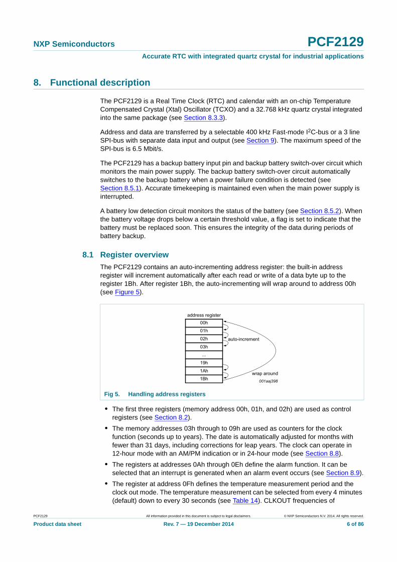
8.1 Register overview
The PCF2129 contains an auto-incrementing address register: the built-in address register will increment automatically after each read or write of a data byte up to the register 1Bh. After register 1Bh, the auto-incrementing will wrap around to address 00h (see Figure 5).
• The first three registers (memory address 00h, 01h, and 02h) are used as control registers (see Section 8.2).
• The memory addresses 03h through to 09h are used as counters for the clock function (seconds up to years). The date is automatically adjusted for months with fewer than 31 days, including corrections for leap years. The clock can operate in 12-hour mode with an AM/PM indication or in 24-hour mode (see Section 8.8).
• The registers at addresses 0Ah through 0Eh define the alarm function. It can be selected that an interrupt is generated when an alarm event occurs (see Section 8.9).
• The register at address 0Fh defines the temperature measurement period and the clock out mode. The temperature measurement can be selected from every 4 minutes (default) down to every 30 seconds (see Table 14). CLKOUT frequencies of
Fig 5. Handling address registers
PCF2129 All information provided in this document is subject to legal disclaimers. © NXP Semiconductors N.V. 2014. All rights reserved.
Product data sheet Rev. 7 — 19 December 2014 6 of 86

NXP Semiconductors PCF2129Accurate RTC with integrated quartz crystal for industrial applications
32.768 kHz (default) down to 1 Hz for use as system clock, microcontroller clock, and so on, can be chosen (see Table 15).
• The registers at addresses 10h and 11h are used for the watchdog timer functions. The watchdog timer has four selectable source clocks allowing for timer periods from less than 1 ms to greater than 4 hours (see Table 52). An interrupt is generated when the watchdog times out.
• The registers at addresses 12h to 18h are used for the timestamp function. When the trigger event happens, the actual time is saved in the timestamp registers (see Section 8.11).
• The register at address 19h is used for the correction of the crystal aging effect (see Section 8.4.1).
• The registers at addresses 1Ah and 1Bh are for internal use only.
• The registers Seconds, Minutes, Hours, Days, Months, and Years are all coded in Binary Coded Decimal (BCD) format to simplify application use. Other registers are either bit-wise or standard binary.
When one of the RTC registers is written or read, the content of all counters is temporarily frozen. This prevents a faulty writing or reading of the clock and calendar during a carry condition (see Section 8.8.8).
PCF2129 All information provided in this document is subject to legal disclaimers. © NXP Semiconductors N.V. 2014. All rights reserved.
Product data sheet Rev. 7 — 19 December 2014 7 of 86

xxxxxxxxxxxxxxxxxxxxx xxxxxxxxxxxxxxxxxxxxxxxxxx xxxxxxx x x x xxxxxxxxxxxxxxxxxxxxxxxxxxxxxx xxxxxxxxxxxxxxxxxxx xx xx xxxxx xxxxxxxxxxxxxxxxxxxxxxxxxxx xxxxxxxxxxxxxxxxxxx xxxxxx xxxxxxxxxxxxxxxxxxxxxxxxxxxxxxxxxxx xxxxxxxxxxxx x x xxxxxxxxxxxxxxxxxxxxx xxxxxxxxxxxxxxxxxxxxxxxxxxxxxx xxxxx xxxxxxxxxxxxxxxxxxxxxxxxxxxxxxxxxxxxxxxxxxxxxxxxxx xxxxxxxx xxxxxxxxxxxxxxxxxxxxxxxxx xxxxxxxxxxxxxxxxxxxx xxx
PC
F21
29
Pro
du
ct data sh
NX
P S
emico
nd
ucto
rsP
CF
2129A
cc
ura
te R
TC
with
inte
gra
ted
qu
artz cry
sta
l for in
du
strial a
pp
licatio
ns
Table 5. Register overviewBit positions labeled as - are not implemented and return 0 when read. Bits labeled as T must always be written with logic 0. Bits labeled as X are undefined at power-on and unchanged by subsequent resets.
Address Register name Bit Reset value Reference
0000 1000 Table 7 on page 10
0000 0000 Table 9 on page 11
0000 0000 Table 11 on page 12
1XXX XXXX Table 22 on page 25
- XXX XXXX Table 25 on page 26
- - XX XXXX Table 27 on page 27
- - XX XXXX
- - XX XXXX Table 29 on page 27
- - - - - XXX Table 31 on page 28
- - - X XXXX Table 34 on page 29
XXXX XXXX Table 37 on page 30
1XXX XXXX Table 39 on page 33
1XXX XXXX Table 41 on page 33
1 - XX XXXX Table 43 on page 34
1 - XX XXXX
1 - XX XXXX Table 45 on page 34
1 - - - - XXX Table 47 on page 35
00X - - 000 Table 13 on page 12
000 - - - 11 Table 49 on page 36
XXXX XXXX Table 51 on page 36
00 - X XXXX Table 58 on page 41
All inform
ation provided
in this docum
ent is subject to leg
al disclaim
ers.©
NX
P S
em
iconductors N
.V. 2014. A
ll rights reserved.
eetR
ev. 7 — 19 D
ecemb
er 2014
8 of 86
7 6 5 4 3 2 1 0
Control registers
00h Control_1 EXT_TEST
T STOP TSF1 POR_OVRD
12_24 MI SI
01h Control_2 MSF WDTF TSF2 AF T TSIE AIE T
02h Control_3 PWRMNG[2:0] BTSE BF BLF BIE BLIE
Time and date registers
03h Seconds OSF SECONDS (0 to 59)
04h Minutes - MINUTES (0 to 59)
05h Hours - - AMPM HOURS (1 to 12) in 12-hour mode
HOURS (0 to 23) in 24-hour mode
06h Days - - DAYS (1 to 31)
07h Weekdays - - - - - WEEKDAYS (0 to 6)
08h Months - - - MONTHS (1 to 12)
09h Years YEARS (0 to 99)
Alarm registers
0Ah Second_alarm AE_S SECOND_ALARM (0 to 59)
0Bh Minute_alarm AE_M MINUTE_ALARM (0 to 59)
0Ch Hour_alarm AE_H - AMPM HOUR_ALARM (1 to 12) in 12-hour mode
HOUR_ALARM (0 to 23) in 24-hour mode
0Dh Day_alarm AE_D - DAY_ALARM (1 to 31)
0Eh Weekday_alarm AE_W - - - - WEEKDAY_ALARM (0 to 6)
CLKOUT control register
0Fh CLKOUT_ctl TCR[1:0] OTPR - - COF[2:0]
Watchdog registers
10h Watchdg_tim_ctl WD_CD T TI_TP - - - TF[1:0]
11h Watchdg_tim_val WATCHDG_TIM_VAL[7:0]
Timestamp registers
12h Timestp_ctl TSM TSOFF - 1_O_16_TIMESTP[4:0]

xxxxxxxxxxxxxxxxxxxxx xxxxxxxxxxxxxxxxxxxxxxxxxx xxxxxxx x x x xxxxxxxxxxxxxxxxxxxxxxxxxxxxxx xxxxxxxxxxxxxxxxxxx xx xx xxxxx xxxxxxxxxxxxxxxxxxxxxxxxxxx xxxxxxxxxxxxxxxxxxx xxxxxx xxxxxxxxxxxxxxxxxxxxxxxxxxxxxxxxxxx xxxxxxxxxxxx x x xxxxxxxxxxxxxxxxxxxxx xxxxxxxxxxxxxxxxxxxxxxxxxxxxxx xxxxx xxxxxxxxxxxxxxxxxxxxxxxxxxxxxxxxxxxxxxxxxxxxxxxxxx xxxxxxxx xxxxxxxxxxxxxxxxxxxxxxxxx xxxxxxxxxxxxxxxxxxxx xxx
PC
F21
29
Pro
du
ct data sh
NX
P S
emico
nd
ucto
rsP
CF
2129A
cc
ura
te R
TC
with
inte
gra
ted
qu
artz cry
sta
l for in
du
strial a
pp
licatio
ns
- XXX XXXX Table 60 on page 41
- XXX XXXX Table 62 on page 42
- - XX XXXX Table 64 on page 42
- - XX XXXX
- - XX XXXX Table 66 on page 43
- - - X XXXX Table 68 on page 43
XXXX XXXX Table 70 on page 43
- - - - 1000 Table 17 on page 14
- - - - - - - - -
- - - - - - - - -
Table 5. Register overview …continuedBit positions labeled as - are not implemented and return 0 when read. Bits labeled as T must always be written with logic 0. Bits labeled as X are undefined at power-on and unchanged by subsequent resets.
Address Register name Bit Reset value Reference
7 6 5 4 3 2 1 0
All inform
ation provided
in this docum
ent is subject to leg
al disclaim
ers.©
NX
P S
em
iconductors N
.V. 2014. A
ll rights reserved.
eetR
ev. 7 — 19 D
ecemb
er 2014
9 of 86
13h Sec_timestp - SECOND_TIMESTP (0 to 59)
14h Min_timestp - MINUTE_TIMESTP (0 to 59)
15h Hour_timestp - - AMPM HOUR_TIMESTP (1 to 12) in 12-hour mode
HOUR_TIMESTP (0 to 23) in 24-hour mode
16h Day_timestp - - DAY_TIMESTP (1 to 31)
17h Mon_timestp - - - MONTH_TIMESTP (1 to 12)
18h Year_timestp YEAR_TIMESTP (0 to 99)
Aging offset register
19h Aging_offset - - - - AO[3:0]
Internal registers
1Ah Internal_reg - - - - - - - -
1Bh Internal_reg - - - - - - - -

NXP Semiconductors PCF2129Accurate RTC with integrated quartz crystal for industrial applications
8.2 Control registers
The first 3 registers of the PCF2129, with the addresses 00h, 01h, and 02h, are used as control registers.
8.2.1 Register Control_1
Table 6. Control_1 - control and status register 1 (address 00h) bit allocationBits labeled as T must always be written with logic 0.
Bit 7 6 5 4 3 2 1 0
Symbol EXT_TEST
T STOP TSF1 POR_OVRD
12_24 MI SI
Reset value
0 0 0 0 1 0 0 0
Table 7. Control_1 - control and status register 1 (address 00h) bit descriptionBits labeled as T must always be written with logic 0.
Bit Symbol Value Description Reference
7 EXT_TEST 0 normal mode Section 8.13
1 external clock test mode
6 T 0 unused -
5 STOP 0 RTC source clock runs Section 8.14
1 RTC clock is stopped;
RTC divider chain flip-flops are asynchronously set logic 0;
CLKOUT at 32.768 kHz, 16.384 kHz, or 8.192 kHz is still available
4 TSF1 0 no timestamp interrupt generated Section 8.11.1
1 flag set when TS input is driven to an intermediate level between power supply and ground;
flag must be cleared to clear interrupt
3 POR_OVRD 0 Power-On Reset Override (PORO) facility disabled;
set logic 0 for normal operation
Section 8.7.2
1 Power-On Reset Override (PORO) sequence reception enabled
2 12_24 0 24-hour mode selected Table 27, Table 43, Table 64
1 12-hour mode selected
1 MI 0 minute interrupt disabled Section 8.12.1
1 minute interrupt enabled
0 SI 0 second interrupt disabled
1 second interrupt enabled
PCF2129 All information provided in this document is subject to legal disclaimers. © NXP Semiconductors N.V. 2014. All rights reserved.
Product data sheet Rev. 7 — 19 December 2014 10 of 86

NXP Semiconductors PCF2129Accurate RTC with integrated quartz crystal for industrial applications
8.2.2 Register Control_2
Table 8. Control_2 - control and status register 2 (address 01h) bit allocationBits labeled as T must always be written with logic 0.
Bit 7 6 5 4 3 2 1 0
Symbol MSF WDTF TSF2 AF T TSIE AIE T
Reset value
0 0 0 0 0 0 0 0
Table 9. Control_2 - control and status register 2 (address 01h) bit descriptionBits labeled as T must always be written with logic 0.
Bit Symbol Value Description Reference
7 MSF 0 no minute or second interrupt generated Section 8.12
1 flag set when minute or second interrupt generated;
flag must be cleared to clear interrupt
6 WDTF 0 no watchdog timer interrupt or reset generated Section 8.12.3
1 flag set when watchdog timer interrupt or reset generated;
flag cannot be cleared by command (read-only)
5 TSF2 0 no timestamp interrupt generated Section 8.11.1
1 flag set when TS input is driven to ground;
flag must be cleared to clear interrupt
4 AF 0 no alarm interrupt generated Section 8.9.6
1 flag set when alarm triggered;
flag must be cleared to clear interrupt
3 T 0 unused -
2 TSIE 0 no interrupt generated from timestamp flag Section 8.12.5
1 interrupt generated when timestamp flag set
1 AIE 0 no interrupt generated from the alarm flag Section 8.12.4
1 interrupt generated when alarm flag set
0 T 0 unused -
PCF2129 All information provided in this document is subject to legal disclaimers. © NXP Semiconductors N.V. 2014. All rights reserved.
Product data sheet Rev. 7 — 19 December 2014 11 of 86

NXP Semiconductors PCF2129Accurate RTC with integrated quartz crystal for industrial applications
8.2.3 Register Control_3
8.3 Register CLKOUT_ctl
Table 10. Control_3 - control and status register 3 (address 02h) bit allocation
Bit 7 6 5 4 3 2 1 0
Symbol PWRMNG[2:0] BTSE BF BLF BIE BLIE
Reset value
0 0 0 0 0 0 0 0
Table 11. Control_3 - control and status register 3 (address 02h) bit description
Bit Symbol Value Description Reference
7 to 5 PWRMNG[2:0] see Table 19
control of the battery switch-over, battery low detection, and extra power fail detection functions
Section 8.5
4 BTSE 0 no timestamp when battery switch-over occurs Section 8.11.4
1 time-stamped when battery switch-over occurs
3 BF 0 no battery switch-over interrupt generated Section 8.5.1 and Section 8.11.4
1 flag set when battery switch-over occurs;
flag must be cleared to clear interrupt
2 BLF 0 battery status ok;
no battery low interrupt generated
Section 8.5.2
1 battery status low;
flag cannot be cleared by command
1 BIE 0 no interrupt generated from the battery flag (BF) Section 8.12.6
1 interrupt generated when BF is set
0 BLIE 0 no interrupt generated from battery low flag (BLF) Section 8.12.7
1 interrupt generated when BLF is set
Table 12. CLKOUT_ctl - CLKOUT control register (address 0Fh) bit allocationBit positions labeled as - are not implemented and return 0 when read. Bits labeled as X are undefined at power-on and unchanged by subsequent resets.
Bit 7 6 5 4 3 2 1 0
Symbol TCR[1:0] OTPR - - COF[2:0]
Reset value
0 0 X - - 0 0 0
Table 13. CLKOUT_ctl - CLKOUT control register (address 0Fh) bit descriptionBit positions labeled as - are not implemented and return 0 when read. Bits labeled as X are undefined at power-on and unchanged by subsequent resets.
Bit Symbol Value Description
7 to 6 TCR[1:0] see Table 14 temperature measurement period
5 OTPR 0 no OTP refresh
1 OTP refresh performed
4 to 3 - - unused
2 to 0 COF[2:0] see Table 15 CLKOUT frequency selection
PCF2129 All information provided in this document is subject to legal disclaimers. © NXP Semiconductors N.V. 2014. All rights reserved.
Product data sheet Rev. 7 — 19 December 2014 12 of 86

NXP Semiconductors PCF2129Accurate RTC with integrated quartz crystal for industrial applications
8.3.1 Temperature compensated crystal oscillator
The frequency of tuning fork quartz crystal oscillators is temperature-dependent. In the PCF2129, the frequency deviation caused by temperature variation is corrected by adjusting the load capacitance of the crystal oscillator.
The load capacitance is changed by switching between two load capacitance values using a modulation signal with a programmable duty cycle. In order to compensate the spread of the quartz parameters every chip is factory calibrated.
The frequency accuracy can be evaluated by measuring the frequency of the square wave signal available at the output pin CLKOUT. However, the selection of fCLKOUT = 32.768 kHz (default value) leads to inaccurate measurements. Accurate frequency measurement occurs when fCLKOUT = 16.384 kHz or lower is selected (see Table 15).
8.3.1.1 Temperature measurement
The PCF2129 has a temperature sensor circuit used to perform the temperature compensation of the frequency. The temperature is measured immediately after power-on and then periodically with a period set by the temperature conversion rate TCR[1:0] in the register CLKOUT_ctl.
[1] Default value.
8.3.2 OTP refresh
Each IC is calibrated during production and testing of the device. The calibration parameters are stored on EPROM cells called One Time Programmable (OTP) cells. It is recommended to process an OTP refresh once after the power is up and the oscillator is operating stable. The OTP refresh takes less than 100 ms to complete.
To perform an OTP refresh, bit OTPR has to be cleared (set to logic 0) and then set to logic 1 again.
8.3.3 Clock output
A programmable square wave is available at pin CLKOUT. Operation is controlled by the COF[2:0] control bits in register CLKOUT_ctl. Frequencies of 32.768 kHz (default) down to 1 Hz can be generated for use as system clock, microcontroller clock, charge pump input, or for calibrating the oscillator.
CLKOUT is an open-drain output and enabled at power-on. When disabled, the output is high-impedance.
Table 14. Temperature measurement period
TCR[1:0] Temperature measurement period
00 [1] 4 min
01 2 min
10 1 min
11 30 seconds
PCF2129 All information provided in this document is subject to legal disclaimers. © NXP Semiconductors N.V. 2014. All rights reserved.
Product data sheet Rev. 7 — 19 December 2014 13 of 86

NXP Semiconductors PCF2129Accurate RTC with integrated quartz crystal for industrial applications
[1] Duty cycle definition: % HIGH-level time : % LOW-level time.
[2] Default value.
[3] The specified accuracy of the RTC can be only achieved with CLKOUT frequencies not equal to 32.768 kHz or if CLKOUT is disabled.
The duty cycle of the selected clock is not controlled, however, due to the nature of the clock generation all but the 32.768 kHz frequencies are 50 : 50.
8.4 Register Aging_offset
8.4.1 Crystal aging correction
The PCF2129 has an offset register Aging_offset to correct the crystal aging effects2.
The accuracy of the frequency of a quartz crystal depends on its aging. The aging offset adds an adjustment, positive or negative, in the temperature compensation circuit which allows correcting the aging effect.
At 25 C, the aging offset bits allow a frequency correction of typically 1 ppm per AO[3:0] value, from 7 ppm to +8 ppm.
Table 15. CLKOUT frequency selection
COF[2:0] CLKOUT frequency (Hz) Typical duty cycle[1]
000 [2][3] 32768 60 : 40 to 40 : 60
001 16384 50 : 50
010 8192 50 : 50
011 4096 50 : 50
100 2048 50 : 50
101 1024 50 : 50
110 1 50 : 50
111 CLKOUT = high-Z -
Table 16. Aging_offset - crystal aging offset register (address 19h) bit allocationBit positions labeled as - are not implemented and return 0 when read.
Bit 7 6 5 4 3 2 1 0
Symbol - - - - AO[3:0]
Reset value
- - - - 1 0 0 0
Table 17. Aging_offset - crystal aging offset register (address 19h) bit descriptionBit positions labeled as - are not implemented and return 0 when read.
Bit Symbol Value Description
7 to 4 - - unused
3 to 0 AO[3:0] see Table 18 aging offset value
2. For further information, refer to the application note Ref. 3 “AN11186”.
PCF2129 All information provided in this document is subject to legal disclaimers. © NXP Semiconductors N.V. 2014. All rights reserved.
Product data sheet Rev. 7 — 19 December 2014 14 of 86

NXP Semiconductors PCF2129Accurate RTC with integrated quartz crystal for industrial applications
[1] Default value.
Table 18. Frequency correction at 25C, typical
AO[3:0] ppm
Decimal Binary
0 0000 +8
1 0001 +7
2 0010 +6
3 0011 +5
4 0100 +4
5 0101 +3
6 0110 +2
7 0111 +1
8 1000 [1] 0
9 1001 1
10 1010 2
11 1011 3
12 1100 4
13 1101 5
14 1110 6
15 1111 7
PCF2129 All information provided in this document is subject to legal disclaimers. © NXP Semiconductors N.V. 2014. All rights reserved.
Product data sheet Rev. 7 — 19 December 2014 15 of 86

NXP Semiconductors PCF2129Accurate RTC with integrated quartz crystal for industrial applications
8.5 Power management functions
The PCF2129 has two power supplies:
VDD — the main power supply
VBAT — the battery backup supply
Internally, the PCF2129 is operating with the internal operating voltage Voper(int) which is also available as VBBS on the battery backed output voltage pin, BBS. Depending on the condition of the main power supply and the selected power management function, Voper(int) is either on the potential of VDD or VBAT (see Section 8.5.3).
Two power management functions are implemented:
Battery switch-over function — monitoring the main power supply VDD and switching to VBAT in case a power fail condition is detected (see Section 8.5.1).
Battery low detection function — monitoring the status of the battery, VBAT (see Section 8.5.2).
The power management functions are controlled by the control bits PWRMNG[2:0] (see Table 19) in register Control_3 (see Table 11):
[1] Default value.
[2] When the battery switch-over function is disabled, the PCF2129 works only with the power supply VDD. VBAT must be put to ground and the battery low detection function is disabled.
Table 19. Power management control bit description
PWRMNG[2:0] Function
000 [1] battery switch-over function is enabled in standard mode;
battery low detection function is enabled
001 battery switch-over function is enabled in standard mode;
battery low detection function is disabled
010 battery switch-over function is enabled in standard mode;
battery low detection function is disabled
011 battery switch-over function is enabled in direct switching mode;
battery low detection function is enabled
100 battery switch-over function is enabled in direct switching mode;
battery low detection function is disabled
101 battery switch-over function is enabled in direct switching mode;
battery low detection function is disabled
111 [2] battery switch-over function is disabled, only one power supply (VDD);
battery low detection function is disabled
PCF2129 All information provided in this document is subject to legal disclaimers. © NXP Semiconductors N.V. 2014. All rights reserved.
Product data sheet Rev. 7 — 19 December 2014 16 of 86

NXP Semiconductors PCF2129Accurate RTC with integrated quartz crystal for industrial applications
8.5.1 Battery switch-over function
The PCF2129 has a backup battery switch-over circuit which monitors the main power supply VDD. When a power failure condition is detected, it automatically switches to the backup battery.
One of two operation modes can be selected:
Standard mode — the power failure condition happens when:VDD < VBAT AND VDD < Vth(sw)bat
Vth(sw)bat is the battery switch threshold voltage. Typical value is 2.5 V. The battery switch-over in standard mode works only for VDD > 2.5 V
Direct switching mode — the power failure condition happens when VDD < VBAT. Direct switching from VDD to VBAT without requiring VDD to drop below Vth(sw)bat
When a power failure condition occurs and the power supply switches to the battery, the following sequence occurs:
1. The battery switch flag BF (register Control_3) is set logic 1.
2. An interrupt is generated if the control bit BIE (register Control_3) is enabled (see Section 8.12.6).
3. If the control bit BTSE (register Control_3) is logic 1, the timestamp registers store the time and date when the battery switch occurred (see Section 8.11.4).
4. The battery switch flag BF is cleared by command; it must be cleared to clear the interrupt.
The interface is disabled in battery backup operation:
• Interface inputs are not recognized, preventing extraneous data being written to the device
• Interface outputs are high-impedance
For further information about I2C-bus communication and battery backup operation, see Section 9.3 on page 56.
PCF2129 All information provided in this document is subject to legal disclaimers. © NXP Semiconductors N.V. 2014. All rights reserved.
Product data sheet Rev. 7 — 19 December 2014 17 of 86

NXP Semiconductors PCF2129Accurate RTC with integrated quartz crystal for industrial applications
8.5.1.1 Standard mode
If VDD > VBAT OR VDD > Vth(sw)bat: Voper(int) is at VDD potential.
If VDD < VBAT AND VDD < Vth(sw)bat: Voper(int) is at VBAT potential.
Vth(sw)bat is the battery switch threshold voltage. Typical value is 2.5 V. In standard mode, the battery switch-over works only for VDD > 2.5 V.
VDD may be lower than VBAT (for example VDD = 3 V, VBAT = 4.1 V).
Fig 6. Battery switch-over behavior in standard mode with bit BIE set logic 1 (enabled)
PCF2129 All information provided in this document is subject to legal disclaimers. © NXP Semiconductors N.V. 2014. All rights reserved.
Product data sheet Rev. 7 — 19 December 2014 18 of 86

NXP Semiconductors PCF2129Accurate RTC with integrated quartz crystal for industrial applications
8.5.1.2 Direct switching mode
If VDD > VBAT: Voper(int) is at VDD potential.
If VDD < VBAT: Voper(int) is at VBAT potential.
The direct switching mode is useful in systems where VDD is always higher than VBAT. This mode is not recommended if the VDD and VBAT values are similar (for example, VDD = 3.3 V, VBAT 3.0 V). In direct switching mode, the power consumption is reduced compared to the standard mode because the monitoring of VDD and Vth(sw)bat is not performed.
8.5.1.3 Battery switch-over disabled: only one power supply (VDD)
When the battery switch-over function is disabled:
• The power supply is applied on the VDD pin
• The VBAT pin must be connected to ground
• Voper(int) is at VDD potential
• The battery flag (BF) is always logic 0
Fig 7. Battery switch-over behavior in direct switching mode with bit BIE set logic 1 (enabled)
PCF2129 All information provided in this document is subject to legal disclaimers. © NXP Semiconductors N.V. 2014. All rights reserved.
Product data sheet Rev. 7 — 19 December 2014 19 of 86

NXP Semiconductors PCF2129Accurate RTC with integrated quartz crystal for industrial applications
8.5.1.4 Battery switch-over architecture
The architecture of the battery switch-over circuit is shown in Figure 8.
Voper(int) is at VDD or VBAT potential.
Remark: It has to be assured that there are decoupling capacitors on the pins VDD, VBAT, and BBS.
8.5.2 Battery low detection function
The PCF2129 has a battery low detection circuit which monitors the status of the battery VBAT.
When VBAT drops below the threshold value Vth(bat)low (typically 2.5 V), the BLF flag (register Control_3) is set to indicate that the battery is low and that it must be replaced. Monitoring of the battery voltage also occurs during battery operation.
An unreliable battery cannot prevent that the supply voltage drops below Vlow (typical 1.2 V) and with that the data integrity gets lost. (For further information about Vlow see Section 8.6.)
When VBAT drops below the threshold value Vth(bat)low, the following sequence occurs (see Figure 9):
1. The battery low flag BLF is set logic 1.
2. An interrupt is generated if the control bit BLIE (register Control_3) is enabled (see Section 8.12.7).
3. The flag BLF remains logic 1 until the battery is replaced. BLF cannot be cleared by command. It is automatically cleared by the battery low detection circuit when the battery is replaced or when the voltage rises again above the threshold value. This could happen if a super capacitor is used as a backup source and the main power is applied again.
Fig 8. Battery switch-over circuit, simplified block diagram
PCF2129 All information provided in this document is subject to legal disclaimers. © NXP Semiconductors N.V. 2014. All rights reserved.
Product data sheet Rev. 7 — 19 December 2014 20 of 86

NXP Semiconductors PCF2129Accurate RTC with integrated quartz crystal for industrial applications
8.5.3 Battery backup supply
The VBBS voltage on the output pin BBS is at the same potential as the internal operating voltage Voper(int), depending on the selected battery switch-over function mode:
The output pin BBS can be used as a supply for external devices with battery backup needs, such as SRAM (see Ref. 3 “AN11186”). For this case, Figure 10 shows the typical driving capability when VBBS is driven from VDD.
Fig 9. Battery low detection behavior with bit BLIE set logic 1 (enabled)
Table 20. Output pin BBS
Battery switch-over function mode
Conditions Potential of Voper(int) and VBBS
standard VDD > VBAT OR VDD > Vth(sw)bat VDD
VDD < VBAT AND VDD < Vth(sw)bat VBAT
direct switching VDD > VBAT VDD
VDD < VBAT VBAT
disabled only VDD available,VBAT must be put to ground
VDD
PCF2129 All information provided in this document is subject to legal disclaimers. © NXP Semiconductors N.V. 2014. All rights reserved.
Product data sheet Rev. 7 — 19 December 2014 21 of 86

NXP Semiconductors PCF2129Accurate RTC with integrated quartz crystal for industrial applications
8.6 Oscillator stop detection function
The PCF2129 has an on-chip oscillator detection circuit which monitors the status of the oscillation: whenever the oscillation stops, a reset occurs and the oscillator stop flag OSF (in register Seconds) is set logic 1.
• Power-on:
a. The oscillator is not running, the chip is in reset (OSF is logic 1).
b. When the oscillator starts running and is stable after power-on, the chip exits from reset.
c. The flag OSF is still logic 1 and can be cleared (OSF set logic 0) by command.
• Power supply failure:
a. When the power supply of the chip drops below a certain value (Vlow), typically 1.2 V, the oscillator stops running and a reset occurs.
b. When the power supply returns to normal operation, the oscillator starts running again, the chip exits from reset.
c. The flag OSF is still logic 1 and can be cleared (OSF set logic 0) by command.
Fig 10. Typical driving capability of VBBS: (VBBS VDD) with respect to the output load current IBBS
PCF2129 All information provided in this document is subject to legal disclaimers. © NXP Semiconductors N.V. 2014. All rights reserved.
Product data sheet Rev. 7 — 19 December 2014 22 of 86

NXP Semiconductors PCF2129Accurate RTC with integrated quartz crystal for industrial applications
8.7 Reset function
The PCF2129 has a Power-On Reset (POR) and a Power-On Reset Override (PORO) function implemented.
8.7.1 Power-On Reset (POR)
The POR is active whenever the oscillator is stopped. The oscillator is considered to be stopped during the time between power-on and stable crystal resonance (see Figure 12). This time may be in the range of 200 ms to 2 s depending on temperature and supply voltage. Whenever an internal reset occurs, the oscillator stop flag is set (OSF set logic 1).
The OTP refresh (see Section 8.3.2 on page 13) should ideally be executed as the first instruction after start-up and also after a reset due to an oscillator stop.
(1) Theoretical state of the signals since there is no power.
(2) The oscillator stop flag (OSF), set logic 1, indicates that the oscillation has stopped and a reset has occurred since the flag was last cleared (OSF set logic 0). In this case, the integrity of the clock information is not guaranteed. The OSF flag is cleared by command.
Fig 11. Power failure event due to battery discharge: reset occurs
PCF2129 All information provided in this document is subject to legal disclaimers. © NXP Semiconductors N.V. 2014. All rights reserved.
Product data sheet Rev. 7 — 19 December 2014 23 of 86

NXP Semiconductors PCF2129Accurate RTC with integrated quartz crystal for industrial applications
After POR, the following mode is entered:
• 32.768 kHz CLKOUT active
• Power-On Reset Override (PORO) available to be set
• 24-hour mode is selected
• Battery switch-over is enabled
• Battery low detection is enabled
The register values after power-on are shown in Table 5 on page 8.
8.7.2 Power-On Reset Override (PORO)
The POR duration is directly related to the crystal oscillator start-up time. Due to the long start-up times experienced by these types of circuits, a mechanism has been built in to disable the POR and therefore speed up the on-board test of the device.
The setting of the PORO mode requires that POR_OVRD in register Control_1 is set logic 1 and that the signals at the interface pins SDA/CE and SCL are toggled as illustrated in Figure 14. All timings shown are required minimum.
Fig 12. Dependency between POR and oscillator
Fig 13. Power-On Reset (POR) system
PCF2129 All information provided in this document is subject to legal disclaimers. © NXP Semiconductors N.V. 2014. All rights reserved.
Product data sheet Rev. 7 — 19 December 2014 24 of 86

NXP Semiconductors PCF2129Accurate RTC with integrated quartz crystal for industrial applications
Once the override mode is entered, the device is immediately released from the reset state and the set-up operation can commence.
The PORO mode is cleared by writing logic 0 to POR_OVRD. POR_OVRD must be logic 1 before a re-entry into the override mode is possible. Setting POR_OVRD logic 0 during normal operation has no effect except to prevent accidental entry into the PORO mode.
8.8 Time and date function
Most of these registers are coded in the Binary Coded Decimal (BCD) format.
8.8.1 Register Seconds
Fig 14. Power-On Reset Override (PORO) sequence, valid for both I2C-bus and SPI-bus
Table 21. Seconds - seconds and clock integrity register (address 03h) bit allocationBits labeled as X are undefined at power-on and unchanged by subsequent resets.
Bit 7 6 5 4 3 2 1 0
Symbol OSF SECONDS (0 to 59)
Reset value
1 X X X X X X X
Table 22. Seconds - seconds and clock integrity register (address 03h) bit descriptionBits labeled as X are undefined at power-on and unchanged by subsequent resets.
Bit Symbol Value Place value Description
7 OSF 0 - clock integrity is guaranteed
1 - clock integrity is not guaranteed:
oscillator has stopped and chip reset has occurred since flag was last cleared
6 to 4 SECONDS 0 to 5 ten’s place actual seconds coded in BCD format
3 to 0 0 to 9 unit place
PCF2129 All information provided in this document is subject to legal disclaimers. © NXP Semiconductors N.V. 2014. All rights reserved.
Product data sheet Rev. 7 — 19 December 2014 25 of 86

NXP Semiconductors PCF2129Accurate RTC with integrated quartz crystal for industrial applications
8.8.2 Register Minutes
Table 23. Seconds coded in BCD format
Seconds value in decimal
Upper-digit (ten’s place) Digit (unit place)
Bit 6 Bit 5 Bit 4 Bit 3 Bit 2 Bit 1 Bit 0
00 0 0 0 0 0 0 0
01 0 0 0 0 0 0 1
02 0 0 0 0 0 1 0
: : : : : : : :
09 0 0 0 1 0 0 1
10 0 0 1 0 0 0 0
: : : : : : : :
58 1 0 1 1 0 0 0
59 1 0 1 1 0 0 1
Table 24. Minutes - minutes register (address 04h) bit allocationBit positions labeled as - are not implemented and return 0 when read. Bits labeled as X are undefined at power-on and unchanged by subsequent resets.
Bit 7 6 5 4 3 2 1 0
Symbol - MINUTES (0 to 59)
Reset value
- X X X X X X X
Table 25. Minutes - minutes register (address 04h) bit descriptionBit positions labeled as - are not implemented and return 0 when read. Bits labeled as X are undefined at power-on and unchanged by subsequent resets.
Bit Symbol Value Place value Description
7 - - - unused
6 to 4 MINUTES 0 to 5 ten’s place actual minutes coded in BCD format
3 to 0 0 to 9 unit place
PCF2129 All information provided in this document is subject to legal disclaimers. © NXP Semiconductors N.V. 2014. All rights reserved.
Product data sheet Rev. 7 — 19 December 2014 26 of 86

NXP Semiconductors PCF2129Accurate RTC with integrated quartz crystal for industrial applications
8.8.3 Register Hours
[1] Hour mode is set by the bit 12_24 in register Control_1 (see Table 7).
8.8.4 Register Days
[1] If the year counter contains a value which is exactly divisible by 4, including the year 00, the RTC compensates for leap years by adding a 29th day to February.
Table 26. Hours - hours register (address 05h) bit allocationBit positions labeled as - are not implemented and return 0 when read. Bits labeled as X are undefined at power-on and unchanged by subsequent resets.
Bit 7 6 5 4 3 2 1 0
Symbol - - AMPM HOURS (1 to 12) in 12-hour mode
HOURS (0 to 23) in 24-hour mode
Reset value
- - X X X X X X
Table 27. Hours - hours register (address 05h) bit descriptionBit positions labeled as - are not implemented and return 0 when read. Bits labeled as X are undefined at power-on and unchanged by subsequent resets.
Bit Symbol Value Place value Description
7 to 6 - - - unused
12-hour mode[1]
5 AMPM 0 - indicates AM
1 - indicates PM
4 HOURS 0 to 1 ten’s place actual hours coded in BCD format when in 12-hour mode3 to 0 0 to 9 unit place
24-hour mode[1]
5 to 4 HOURS 0 to 2 ten’s place actual hours coded in BCD format when in 24-hour mode3 to 0 0 to 9 unit place
Table 28. Days - days register (address 06h) bit allocationBit positions labeled as - are not implemented and return 0 when read. Bits labeled as X are undefined at power-on and unchanged by subsequent resets.
Bit 7 6 5 4 3 2 1 0
Symbol - - DAYS (1 to 31)
Reset value
- - X X X X X X
Table 29. Days - days register (address 06h) bit description
Bit Symbol Value Place value Description
7 to 6 - - - unused
5 to 4 DAYS[1] 0 to 3 ten’s place actual day coded in BCD format
3 to 0 0 to 9 unit place
PCF2129 All information provided in this document is subject to legal disclaimers. © NXP Semiconductors N.V. 2014. All rights reserved.
Product data sheet Rev. 7 — 19 December 2014 27 of 86

NXP Semiconductors PCF2129Accurate RTC with integrated quartz crystal for industrial applications
8.8.5 Register Weekdays
Although the association of the weekdays counter to the actual weekday is arbitrary, the PCF2129 assumes that Sunday is 000 and Monday is 001 for the purpose of determining the increment for calendar weeks.
[1] Definition may be reassigned by the user.
Table 30. Weekdays - weekdays register (address 07h) bit allocationBit positions labeled as - are not implemented and return 0 when read. Bits labeled as X are undefined at power-on and unchanged by subsequent resets.
Bit 7 6 5 4 3 2 1 0
Symbol - - - - - WEEKDAYS (0 to 6)
Reset value
- - - - - X X X
Table 31. Weekdays - weekdays register (address 07h) bit descriptionBit positions labeled as - are not implemented and return 0 when read. Bits labeled as X are undefined at power-on and unchanged by subsequent resets.
Bit Symbol Value Description
7 to 3 - - unused
2 to 0 WEEKDAYS 0 to 6 actual weekday value, see Table 32
Table 32. Weekday assignments
Day[1] Bit
2 1 0
Sunday 0 0 0
Monday 0 0 1
Tuesday 0 1 0
Wednesday 0 1 1
Thursday 1 0 0
Friday 1 0 1
Saturday 1 1 0
PCF2129 All information provided in this document is subject to legal disclaimers. © NXP Semiconductors N.V. 2014. All rights reserved.
Product data sheet Rev. 7 — 19 December 2014 28 of 86

NXP Semiconductors PCF2129Accurate RTC with integrated quartz crystal for industrial applications
8.8.6 Register Months
Table 33. Months - months register (address 08h) bit allocationBit positions labeled as - are not implemented and return 0 when read. Bits labeled as X are undefined at power-on and unchanged by subsequent resets.
Bit 7 6 5 4 3 2 1 0
Symbol - - - MONTHS (1 to 12)
Reset value
- - - X X X X X
Table 34. Months - months register (address 08h) bit descriptionBit positions labeled as - are not implemented and return 0 when read. Bits labeled as X are undefined at power-on and unchanged by subsequent resets.
Bit Symbol Value Place value Description
7 to 5 - - - unused
4 MONTHS 0 to 1 ten’s place actual month coded in BCD format, see Table 35
3 to 0 0 to 9 unit place
Table 35. Month assignments in BCD format
Month Upper-digit (ten’s place)
Digit (unit place)
Bit 4 Bit 3 Bit 2 Bit 1 Bit 0
January 0 0 0 0 1
February 0 0 0 1 0
March 0 0 0 1 1
April 0 0 1 0 0
May 0 0 1 0 1
June 0 0 1 1 0
July 0 0 1 1 1
August 0 1 0 0 0
September 0 1 0 0 1
October 1 0 0 0 0
November 1 0 0 0 1
December 1 0 0 1 0
PCF2129 All information provided in this document is subject to legal disclaimers. © NXP Semiconductors N.V. 2014. All rights reserved.
Product data sheet Rev. 7 — 19 December 2014 29 of 86

NXP Semiconductors PCF2129Accurate RTC with integrated quartz crystal for industrial applications
8.8.7 Register Years
8.8.8 Setting and reading the time
Figure 15 shows the data flow and data dependencies starting from the 1 Hz clock tick.
During read/write operations, the time counting circuits (memory locations 03h through 09h) are blocked.
This prevents
• Faulty reading of the clock and calendar during a carry condition
• Incrementing the time registers during the read cycle
After this read/write access is completed, the time circuit is released again. Any pending request to increment the time counters that occurred during the read/write access is serviced. A maximum of 1 request can be stored; therefore, all accesses must be completed within 1 second (see Figure 16).
Table 36. Years - years register (address 09h) bit allocationBits labeled as X are undefined at power-on and unchanged by subsequent resets.
Bit 7 6 5 4 3 2 1 0
Symbol YEARS (0 to 99)
Reset value
X X X X X X X X
Table 37. Years - years register (address 09h) bit descriptionBits labeled as X are undefined at power-on and unchanged by subsequent resets.
Bit Symbol Value Place value Description
7 to 4 YEARS 0 to 9 ten’s place actual year coded in BCD format
3 to 0 0 to 9 unit place
Fig 15. Data flow of the time function
PCF2129 All information provided in this document is subject to legal disclaimers. © NXP Semiconductors N.V. 2014. All rights reserved.
Product data sheet Rev. 7 — 19 December 2014 30 of 86

NXP Semiconductors PCF2129Accurate RTC with integrated quartz crystal for industrial applications
As a consequence of this method, it is very important to make a read or write access in one go. That is, setting or reading seconds through to years should be made in one single access. Failing to comply with this method could result in the time becoming corrupted.
As an example, if the time (seconds through to hours) is set in one access and then in a second access the date is set, it is possible that the time may increment between the two accesses. A similar problem exists when reading. A roll-over may occur between reads thus giving the minutes from one moment and the hours from the next. Therefore it is advised to read all time and date registers in one access.
Fig 16. Access time for read/write operations
PCF2129 All information provided in this document is subject to legal disclaimers. © NXP Semiconductors N.V. 2014. All rights reserved.
Product data sheet Rev. 7 — 19 December 2014 31 of 86

NXP Semiconductors PCF2129Accurate RTC with integrated quartz crystal for industrial applications
8.9 Alarm function
When one or more of the alarm bit fields are loaded with a valid second, minute, hour, day, or weekday and its corresponding alarm enable bit (AE_x) is logic 0, then that information is compared with the actual second, minute, hour, day, and weekday (see Figure 17).
The generation of interrupts from the alarm function is described in Section 8.12.4.
(1) Only when all enabled alarm settings are matching.
Fig 17. Alarm function block diagram
PCF2129 All information provided in this document is subject to legal disclaimers. © NXP Semiconductors N.V. 2014. All rights reserved.
Product data sheet Rev. 7 — 19 December 2014 32 of 86

NXP Semiconductors PCF2129Accurate RTC with integrated quartz crystal for industrial applications
8.9.1 Register Second_alarm
8.9.2 Register Minute_alarm
Table 38. Second_alarm - second alarm register (address 0Ah) bit allocationBits labeled as X are undefined at power-on and unchanged by subsequent resets.
Bit 7 6 5 4 3 2 1 0
Symbol AE_S SECOND_ALARM (0 to 59)
Reset value
1 X X X X X X X
Table 39. Second_alarm - second alarm register (address 0Ah) bit description
Bit Symbol Value Place value Description
7 AE_S 0 - second alarm is enabled
1 - second alarm is disabled
6 to 4 SECOND_ALARM 0 to 5 ten’s place second alarm information coded in BCD format
3 to 0 0 to 9 unit place
Table 40. Minute_alarm - minute alarm register (address 0Bh) bit allocationBits labeled as X are undefined at power-on and unchanged by subsequent resets.
Bit 7 6 5 4 3 2 1 0
Symbol AE_M MINUTE_ALARM (0 to 59)
Reset value
1 X X X X X X X
Table 41. Minute_alarm - minute alarm register (address 0Bh) bit descriptionBits labeled as X are undefined at power-on and unchanged by subsequent resets.
Bit Symbol Value Place value Description
7 AE_M 0 - minute alarm is enabled
1 - minute alarm is disabled
6 to 4 MINUTE_ALARM 0 to 5 ten’s place minute alarm information coded in BCD format
3 to 0 0 to 9 unit place
PCF2129 All information provided in this document is subject to legal disclaimers. © NXP Semiconductors N.V. 2014. All rights reserved.
Product data sheet Rev. 7 — 19 December 2014 33 of 86

NXP Semiconductors PCF2129Accurate RTC with integrated quartz crystal for industrial applications
8.9.3 Register Hour_alarm
[1] Hour mode is set by the bit 12_24 in register Control_1.
8.9.4 Register Day_alarm
Table 42. Hour_alarm - hour alarm register (address 0Ch) bit allocationBit positions labeled as - are not implemented and return 0 when read. Bits labeled as X are undefined at power-on and unchanged by subsequent resets.
Bit 7 6 5 4 3 2 1 0
Symbol AE_H - AMPM HOUR_ALARM (1 to 12) in 12-hour mode
HOUR_ALARM (0 to 23) in 24-hour mode
Reset value
1 - X X X X X X
Table 43. Hour_alarm - hour alarm register (address 0Ch) bit descriptionBit positions labeled as - are not implemented and return 0 when read. Bits labeled as X are undefined at power-on and unchanged by subsequent resets.
Bit Symbol Value Place value Description
7 AE_H 0 - hour alarm is enabled
1 - hour alarm is disabled
6 - - - unused
12-hour mode[1]
5 AMPM 0 - indicates AM
1 - indicates PM
4 HOUR_ALARM 0 to 1 ten’s place hour alarm information coded in BCD format when in 12-hour mode3 to 0 0 to 9 unit place
24-hour mode[1]
5 to 4 HOUR_ALARM 0 to 2 ten’s place hour alarm information coded in BCD format when in 24-hour mode3 to 0 0 to 9 unit place
Table 44. Day_alarm - day alarm register (address 0Dh) bit allocationBit positions labeled as - are not implemented and return 0 when read. Bits labeled as X are undefined at power-on and unchanged by subsequent resets.
Bit 7 6 5 4 3 2 1 0
Symbol AE_D - DAY_ALARM (1 to 31)
Reset value
1 - X X X X X X
Table 45. Day_alarm - day alarm register (address 0Dh) bit descriptionBit positions labeled as - are not implemented and return 0 when read. Bits labeled as X are undefined at power-on and unchanged by subsequent resets.
Bit Symbol Value Place value Description
7 AE_D 0 - day alarm is enabled
1 - day alarm is disabled
6 - - - unused
5 to 4 DAY_ALARM 0 to 3 ten’s place day alarm information coded in BCD format
3 to 0 0 to 9 unit place
PCF2129 All information provided in this document is subject to legal disclaimers. © NXP Semiconductors N.V. 2014. All rights reserved.
Product data sheet Rev. 7 — 19 December 2014 34 of 86

NXP Semiconductors PCF2129Accurate RTC with integrated quartz crystal for industrial applications
8.9.5 Register Weekday_alarm
8.9.6 Alarm flag
When all enabled comparisons first match, the alarm flag AF (register Control_2) is set. AF remains set until cleared by command. Once AF has been cleared, it will only be set again when the time increments to match the alarm condition once more. For clearing the flags, see Section 8.10.5
Alarm registers which have their alarm enable bit AE_x at logic 1 are ignored.
8.10 Timer functions
The PCF2129 has a watchdog timer function. The timer can be switched on and off by using the control bit WD_CD in the register Watchdg_tim_ctl.
The watchdog timer has four selectable source clocks. It can, for example, be used to detect a microcontroller with interrupt and reset capability which is out of control (see Section 8.10.3)
To control the timer function and timer output, the registers Control_2, Watchdg_tim_ctl, and Watchdg_tim_val are used.
Table 46. Weekday_alarm - weekday alarm register (address 0Eh) bit allocationBit positions labeled as - are not implemented and return 0 when read. Bits labeled as X are undefined at power-on and unchanged by subsequent resets.
Bit 7 6 5 4 3 2 1 0
Symbol AE_W - - - - WEEKDAY_ALARM (0 to 6)
Reset value
1 - - - - X X X
Table 47. Weekday_alarm - weekday alarm register (address 0Eh) bit descriptionBit positions labeled as - are not implemented and return 0 when read. Bits labeled as X are undefined at power-on and unchanged by subsequent resets.
Bit Symbol Value Description
7 AE_W 0 weekday alarm is enabled
1 weekday alarm is disabled
6 to 3 - - unused
2 to 0 WEEKDAY_ALARM 0 to 6 weekday alarm information
Example where only the minute alarm is used and no other interrupts are enabled.
Fig 18. Alarm flag timing diagram
PCF2129 All information provided in this document is subject to legal disclaimers. © NXP Semiconductors N.V. 2014. All rights reserved.
Product data sheet Rev. 7 — 19 December 2014 35 of 86

NXP Semiconductors PCF2129Accurate RTC with integrated quartz crystal for industrial applications
8.10.1 Register Watchdg_tim_ctl
8.10.2 Register Watchdg_tim_val
Table 48. Watchdg_tim_ctl - watchdog timer control register (address 10h) bit allocationBit positions labeled as - are not implemented and return 0 when read. Bits labeled as T must always be written with logic 0.
Bit 7 6 5 4 3 2 1 0
Symbol WD_CD T TI_TP - - - TF[1:0]
Reset value
0 0 0 - - - 1 1
Table 49. Watchdg_tim_ctl - watchdog timer control register (address 10h) bit descriptionBit positions labeled as - are not implemented and return 0 when read. Bits labeled as T must always be written with logic 0.
Bit Symbol Value Description
7 WD_CD 0 watchdog timer disabled
1 watchdog timer enabled;
the interrupt pin INT is activated when timed out
6 T 0 unused
5 TI_TP 0 the interrupt pin INT is configured to generate a permanent active signal when MSF is set
1 the interrupt pin INT is configured to generate a pulsed signal when MSF flag is set (see Figure 21)
4 to 2 - - unused
1 to 0 TF[1:0] timer source clock for watchdog timer
00 4.096 kHz
01 64 Hz
10 1 Hz
11 1⁄60 Hz
Table 50. Watchdg_tim_val - watchdog timer value register (address 11h) bit allocationBits labeled as X are undefined at power-on and unchanged by subsequent resets.
Bit 7 6 5 4 3 2 1 0
Symbol WATCHDG_TIM_VAL[7:0]
Reset value
X X X X X X X X
Table 51. Watchdg_tim_val - watchdog timer value register (address 11h) bit descriptionBits labeled as X are undefined at power-on and unchanged by subsequent resets.
Bit Symbol Value Description
7 to 0 WATCHDG_TIM_ VAL[7:0]
00 to FF timer period in seconds:
where n is the timer value
TimerPeriod nSourceClockFrequency---------------------------------------------------------------=
PCF2129 All information provided in this document is subject to legal disclaimers. © NXP Semiconductors N.V. 2014. All rights reserved.
Product data sheet Rev. 7 — 19 December 2014 36 of 86

NXP Semiconductors PCF2129Accurate RTC with integrated quartz crystal for industrial applications
8.10.3 Watchdog timer function
The watchdog timer function is enabled or disabled by the WD_CD bit of the register Watchdg_tim_ctl (see Table 49).
The 2 bits TF[1:0] in register Watchdg_tim_ctl determine one of the four source clock frequencies for the watchdog timer: 4.096 kHz, 64 Hz, 1 Hz, or 1⁄60 Hz (see Table 52).
When the watchdog timer function is enabled, the 8-bit timer in register Watchdg_tim_val determines the watchdog timer period (see Table 52).
The watchdog timer counts down from the software programmed 8-bit binary value n in register Watchdg_tim_val. When the counter reaches 1, the watchdog timer flag WDTF (register Control_2) is set logic 1 and an interrupt is generated.
The counter does not automatically reload.
When WD_CD is logic 0 (watchdog timer disabled) and the Microcontroller Unit (MCU) loads a watchdog timer value n:
• the flag WDTF is reset
• INT is cleared
• the watchdog timer starts again
Loading the counter with 0 will:
• reset the flag WDTF
• clear INT
• stop the watchdog timer
Remark: WDTF is read only and cannot be cleared by command. WDTF can be cleared by:
• loading a value in register Watchdg_tim_val
• reading of the register Control_2
Writing a logic 0 or logic 1 to WDTF has no effect.
Table 52. Programmable watchdog timer
TF[1:0] Timer source clock frequency
Units Minimum timer period (n = 1)
Units Maximum timer period (n = 255)
Units
00 4.096 kHz 244 s 62.256 ms
01 64 Hz 15.625 ms 3.984 s
10 1 Hz 1 s 255 s
11 1⁄60 Hz 60 s 15300 s
PCF2129 All information provided in this document is subject to legal disclaimers. © NXP Semiconductors N.V. 2014. All rights reserved.
Product data sheet Rev. 7 — 19 December 2014 37 of 86

NXP Semiconductors PCF2129Accurate RTC with integrated quartz crystal for industrial applications
• When the watchdog timer counter reaches 1, the watchdog timer flag WDTF is set logic 1
• When a minute or second interrupt occurs, the minute/second flag MSF is set logic 1 (see Section 8.12.1).
8.10.4 Pre-defined timers: second and minute interrupt
PCF2129 has two pre-defined timers which are used to generate an interrupt either once per second or once per minute (see Section 8.12.1). The pulse generator for the minute or second interrupt operates from an internal 64 Hz clock. It is independent of the watchdog timer. Each of these timers can be enabled by the bits SI (second interrupt) and MI (minute interrupt) in register Control_1.
8.10.5 Clearing flags
The flags MSF, AF, and TSFx can be cleared by command. To prevent one flag being overwritten while clearing another, a logic AND is performed during the write access. A flag is cleared by writing logic 0 while a flag is not cleared by writing logic 1. Writing logic 1 results in the flag value remaining unchanged.
Two examples are given for clearing the flags. Clearing a flag is made by a write command:
• Bits labeled with - must be written with their previous values
• Bits labeled with T have to be written with logic 0
• WDTF is read only and has to be written with logic 0
Repeatedly rewriting these bits has no influence on the functional behavior.
Counter reached 1, WDTF is logic 1, and an interrupt is generated.
Fig 19. WD_CD set logic 1: watchdog activates an interrupt when timed out
Table 53. Flag location in register Control_2
Register Bit
7 6 5 4 3 2 1 0
Control_2 MSF WDTF TSF2 AF T - - T
PCF2129 All information provided in this document is subject to legal disclaimers. © NXP Semiconductors N.V. 2014. All rights reserved.
Product data sheet Rev. 7 — 19 December 2014 38 of 86

NXP Semiconductors PCF2129Accurate RTC with integrated quartz crystal for industrial applications
The following tables show what instruction must be sent to clear the appropriate flag.
[1] The bits labeled as - have to be rewritten with the previous values.
[1] The bits labeled as - have to be rewritten with the previous values.
8.11 Timestamp function
The PCF2129 has an active LOW timestamp input pin TS, internally pulled with an on-chip pull-up resistor to Voper(int). It also has a timestamp detection circuit which can detect two different events:
1. Input on pin TS is driven to an intermediate level between power supply and ground.
2. Input on pin TS is driven to ground.
The timestamp function is enabled by default after power-on and it can be switched off by setting the control bit TSOFF (register Timestp_ctl).
Table 54. Example values in register Control_2
Register Bit
7 6 5 4 3 2 1 0
Control_2 1 0 1 1 0 0 0 0
Table 55. Example to clear only AF (bit 4)
Register Bit
7 6 5 4 3 2 1 0
Control_2 1 0 1 0 0 0[1] 0[1] 0
Table 56. Example to clear only MSF (bit 7)
Register Bit
7 6 5 4 3 2 1 0
Control_2 0 0 1 1 0 0[1] 0[1] 0
(1) When using switches or push-buttons, it is recommended to connect a 1 nF capacitance to the TS pin to ensure proper switching.
Fig 20. Timestamp detection with two push-buttons on the TS pin (for example, for tamper detection)
PCF2129 All information provided in this document is subject to legal disclaimers. © NXP Semiconductors N.V. 2014. All rights reserved.
Product data sheet Rev. 7 — 19 December 2014 39 of 86

NXP Semiconductors PCF2129Accurate RTC with integrated quartz crystal for industrial applications
A most common application of the timestamp function is described in Ref. 3 “AN11186”.
See Section 8.12.5 for a description of interrupt generation from the timestamp function.
8.11.1 Timestamp flag
1. When the TS input pin is driven to an intermediate level between the power supply and ground, either on the falling edge from VDD or on the rising edge from ground, then the following sequence occurs:
a. The actual date and time are stored in the timestamp registers.
b. The timestamp flag TSF1 (register Control_1) is set.
c. If the TSIE bit (register Control_2) is active, an interrupt on the INT pin is generated.
The TSF1 flag can be cleared by command. Clearing the flag clears the interrupt. Once TSF1 is cleared, it will only be set again when a new negative or positive edge on pin TS is detected.
2. When the TS input pin is driven to ground, the following sequence occurs:
a. The actual date and time are stored in the timestamp registers.
b. In addition to the TSF1 flag, the TSF2 flag (register Control_2) is set.
c. If the TSIE bit is active, an interrupt on the INT pin is generated.
The TSF1 and TSF2 flags can be cleared by command; clearing both flags clears the interrupt. Once TSF2 is cleared, it will only be set again when TS pin is driven to ground once again.
8.11.2 Timestamp mode
The timestamp function has two different modes selected by the control bit TSM (timestamp mode) in register Timestp_ctl:
• If TSM is logic 0 (default): in subsequent trigger events without clearing the timestamp flags, the last timestamp event is stored
• If TSM is logic 1: in subsequent trigger events without clearing the timestamp flags, the first timestamp event is stored
The timestamp function also depends on the control bit BTSE in register Control_3, see Section 8.11.4.
PCF2129 All information provided in this document is subject to legal disclaimers. © NXP Semiconductors N.V. 2014. All rights reserved.
Product data sheet Rev. 7 — 19 December 2014 40 of 86

NXP Semiconductors PCF2129Accurate RTC with integrated quartz crystal for industrial applications
8.11.3 Timestamp registers
8.11.3.1 Register Timestp_ctl
8.11.3.2 Register Sec_timestp
Table 57. Timestp_ctl - timestamp control register (address 12h) bit allocationBit positions labeled as - are not implemented and return 0 when read. Bits labeled as X are undefined at power-on and unchanged by subsequent resets.
Bit 7 6 5 4 3 2 1 0
Symbol TSM TSOFF - 1_O_16_TIMESTP[4:0]
Reset value
0 0 - X X X X X
Table 58. Timestp_ctl - timestamp control register (address 12h) bit descriptionBit positions labeled as - are not implemented and return 0 when read. Bits labeled as X are undefined at power-on and unchanged by subsequent resets.
Bit Symbol Value Description
7 TSM 0 in subsequent events without clearing the timestamp flags, the last event is stored
1 in subsequent events without clearing the timestamp flags, the first event is stored
6 TSOFF 0 timestamp function active
1 timestamp function disabled
5 - - unused
4 to 0 1_O_16_TIMESTP[4:0] 1⁄16 second timestamp information coded in BCD format
Table 59. Sec_timestp - second timestamp register (address 13h) bit allocationBit positions labeled as - are not implemented and return 0 when read. Bits labeled as X are undefined at power-on and unchanged by subsequent resets.
Bit 7 6 5 4 3 2 1 0
Symbol - SECOND_TIMESTP (0 to 59)
Reset value
- X X X X X X X
Table 60. Sec_timestp - second timestamp register (address 13h) bit descriptionBit positions labeled as - are not implemented and return 0 when read. Bits labeled as X are undefined at power-on and unchanged by subsequent resets.
Bit Symbol Value Place value Description
7 - - - unused
6 to 4 SECOND_TIMESTP 0 to 5 ten’s place second timestamp information coded in BCD format
3 to 0 0 to 9 unit place
PCF2129 All information provided in this document is subject to legal disclaimers. © NXP Semiconductors N.V. 2014. All rights reserved.
Product data sheet Rev. 7 — 19 December 2014 41 of 86

NXP Semiconductors PCF2129Accurate RTC with integrated quartz crystal for industrial applications
8.11.3.3 Register Min_timestp
8.11.3.4 Register Hour_timestp
[1] Hour mode is set by the bit 12_24 in register Control_1.
Table 61. Min_timestp - minute timestamp register (address 14h) bit allocationBit positions labeled as - are not implemented and return 0 when read. Bits labeled as X are undefined at power-on and unchanged by subsequent resets.
Bit 7 6 5 4 3 2 1 0
Symbol - MINUTE_TIMESTP (0 to 59)
Reset value
- X X X X X X X
Table 62. Min_timestp - minute timestamp register (address 14h) bit description Bit positions labeled as - are not implemented and return 0 when read. Bits labeled as X are undefined at power-on and unchanged by subsequent resets.
Bit Symbol Value Place value Description
7 - - - unused
6 to 4 MINUTE_TIMESTP 0 to 5 ten’s place minute timestamp information coded in BCD format
3 to 0 0 to 9 unit place
Table 63. Hour_timestp - hour timestamp register (address 15h) bit allocationBit positions labeled as - are not implemented and return 0 when read. Bits labeled as X are undefined at power-on and unchanged by subsequent resets.
Bit 7 6 5 4 3 2 1 0
Symbol - - AMPM HOUR_TIMESTP (1 to 12) in 12-hour mode
HOUR_TIMESTP (0 to 23) in 24-hour mode
Reset value
- - X X X X X X
Table 64. Hour_timestp - hour timestamp register (address 15h) bit descriptionBit positions labeled as - are not implemented and return 0 when read. Bits labeled as X are undefined at power-on and unchanged by subsequent resets.
Bit Symbol Value Place value Description
7 to 6 - - - unused
12-hour mode[1]
5 AMPM 0 - indicates AM
1 - indicates PM
4 HOUR_TIMESTP 0 to 1 ten’s place hour timestamp information coded in BCD format when in 12-hour mode3 to 0 0 to 9 unit place
24-hour mode[1]
5 to 4 HOUR_TIMESTP 0 to 2 ten’s place hour timestamp information coded in BCD format when in 24-hour mode3 to 0 0 to 9 unit place
PCF2129 All information provided in this document is subject to legal disclaimers. © NXP Semiconductors N.V. 2014. All rights reserved.
Product data sheet Rev. 7 — 19 December 2014 42 of 86

NXP Semiconductors PCF2129Accurate RTC with integrated quartz crystal for industrial applications
8.11.3.5 Register Day_timestp
8.11.3.6 Register Mon_timestp
8.11.3.7 Register Year_timestp
Table 65. Day_timestp - day timestamp register (address 16h) bit allocationBit positions labeled as - are not implemented and return 0 when read. Bits labeled as X are undefined at power-on and unchanged by subsequent resets.
Bit 7 6 5 4 3 2 1 0
Symbol - - DAY_TIMESTP (1 to 31)
Reset value
- - X X X X X X
Table 66. Day_timestp - day timestamp register (address 16h) bit descriptionBit positions labeled as - are not implemented and return 0 when read. Bits labeled as X are undefined at power-on and unchanged by subsequent resets.
Bit Symbol Value Place value Description
7 to 6 - - - unused
5 to 4 DAY_TIMESTP 0 to 3 ten’s place day timestamp information coded in BCD format
3 to 0 0 to 9 unit place
Table 67. Mon_timestp - month timestamp register (address 17h) bit allocationBit positions labeled as - are not implemented and return 0 when read. Bits labeled as X are undefined at power-on and unchanged by subsequent resets.
Bit 7 6 5 4 3 2 1 0
Symbol - - - MONTH_TIMESTP (1 to 12)
Reset value
- - - X X X X X
Table 68. Mon_timestp - month timestamp register (address 17h) bit descriptionBit positions labeled as - are not implemented and return 0 when read. Bits labeled as X are undefined at power-on and unchanged by subsequent resets.
Bit Symbol Value Place value Description
7 to 5 - - - unused
4 MONTH_TIMESTP 0 to 1 ten’s place month timestamp information coded in BCD format
3 to 0 0 to 9 unit place
Table 69. Year_timestp - year timestamp register (address 18h) bit allocationBits labeled as X are undefined at power-on and unchanged by subsequent resets.
Bit 7 6 5 4 3 2 1 0
Symbol YEAR_TIMESTP (0 to 99)
Reset value
X X X X X X X X
Table 70. Year_timestp - year timestamp register (address 18h) bit descriptionBits labeled as X are undefined at power-on and unchanged by subsequent resets.
Bit Symbol Value Place value Description
7 to 4 YEAR_TIMESTP 0 to 9 ten’s place year timestamp information coded in BCD format
3 to 0 0 to 9 unit place
PCF2129 All information provided in this document is subject to legal disclaimers. © NXP Semiconductors N.V. 2014. All rights reserved.
Product data sheet Rev. 7 — 19 December 2014 43 of 86
NXP Semiconductors PCF2129Accurate RTC with integrated quartz crystal for industrial applications
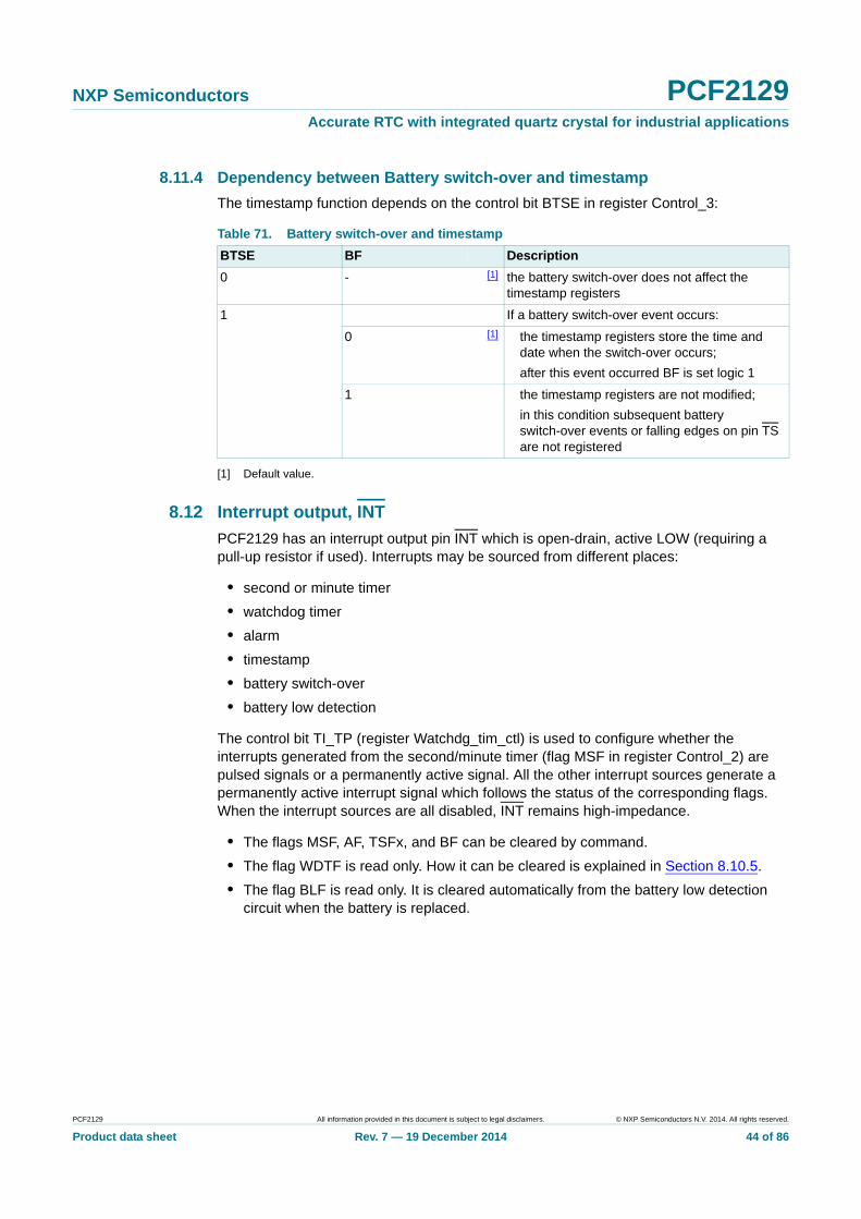
8.11.4 Dependency between Battery switch-over and timestamp
The timestamp function depends on the control bit BTSE in register Control_3:
[1] Default value.
8.12 Interrupt output, INT
PCF2129 has an interrupt output pin INT which is open-drain, active LOW (requiring a pull-up resistor if used). Interrupts may be sourced from different places:
• second or minute timer
• watchdog timer
• alarm
• timestamp
• battery switch-over
• battery low detection
The control bit TI_TP (register Watchdg_tim_ctl) is used to configure whether the interrupts generated from the second/minute timer (flag MSF in register Control_2) are pulsed signals or a permanently active signal. All the other interrupt sources generate a permanently active interrupt signal which follows the status of the corresponding flags. When the interrupt sources are all disabled, INT remains high-impedance.
• The flags MSF, AF, TSFx, and BF can be cleared by command.
• The flag WDTF is read only. How it can be cleared is explained in Section 8.10.5.
• The flag BLF is read only. It is cleared automatically from the battery low detection circuit when the battery is replaced.
Table 71. Battery switch-over and timestamp
BTSE BF Description
0 - [1] the battery switch-over does not affect the timestamp registers
1 If a battery switch-over event occurs:
0 [1] the timestamp registers store the time and date when the switch-over occurs;
after this event occurred BF is set logic 1
1 the timestamp registers are not modified;
in this condition subsequent battery switch-over events or falling edges on pin TS are not registered
PCF2129 All information provided in this document is subject to legal disclaimers. © NXP Semiconductors N.V. 2014. All rights reserved.
Product data sheet Rev. 7 — 19 December 2014 44 of 86

NXP Semiconductors PCF2129Accurate RTC with integrated quartz crystal for industrial applications
8.12.1 Minute and second interrupts
Minute and second interrupts are generated by predefined timers. The timers can be enabled independently from one another by the bits MI and SI in register Control_1. However, a minute interrupt enabled on top of a second interrupt cannot be distinguishable since it occurs at the same time.
The minute/second flag MSF (register Control_2) is set logic 1 when either the seconds or the minutes counter increments according to the enabled interrupt (see Table 72). The MSF flag can be cleared by command.
When SI, MI, WD_CD, AIE, TSIE, BIE, BLIE are all disabled, INT remains high-impedance.
Fig 21. Interrupt block diagram
PCF2129 All information provided in this document is subject to legal disclaimers. © NXP Semiconductors N.V. 2014. All rights reserved.
Product data sheet Rev. 7 — 19 December 2014 45 of 86

NXP Semiconductors PCF2129Accurate RTC with integrated quartz crystal for industrial applications
When MSF is set logic 1:
• If TI_TP is logic 1, the interrupt is generated as a pulsed signal.
• If TI_TP is logic 0, the interrupt is permanently active signal that remains until MSF is cleared.
Table 72. Effect of bits MI and SI on pin INT and bit MSF
MI SI Result on INT Result on MSF
0 0 no interrupt generated MSF never set
1 0 an interrupt once per minute MSF set when minutes counter increments
0 1 an interrupt once per second MSF set when seconds counter increments
1 1 an interrupt once per second MSF set when seconds counter increments
In this example, bit TI_TP is logic 1 and the MSF flag is not cleared after an interrupt.
Fig 22. INT example for SI and MI when TI_TP is logic 1
In this example, bit TI_TP is logic 0 and the MSF flag is cleared after an interrupt.
Fig 23. INT example for SI and MI when TI_TP is logic 0
PCF2129 All information provided in this document is subject to legal disclaimers. © NXP Semiconductors N.V. 2014. All rights reserved.
Product data sheet Rev. 7 — 19 December 2014 46 of 86

NXP Semiconductors PCF2129Accurate RTC with integrated quartz crystal for industrial applications
The pulse generator for the minute/second interrupt operates from an internal 64 Hz clock and generates a pulse of 1⁄64 seconds in duration.
8.12.2 INT pulse shortening
If the MSF flag (register Control_2) is cleared before the end of the INT pulse, then the INT pulse is shortened. This allows the source of a system interrupt to be cleared immediately when it is serviced, that is, the system does not have to wait for the completion of the pulse before continuing; see Figure 24. Instructions for clearing the bit MSF can be found in Section 8.10.5.
8.12.3 Watchdog timer interrupts
The generation of interrupts from the watchdog timer is controlled using the WD_CD bit (register Watchdg_tim_ctl). The interrupt is generated as an active signal which follows the status of the watchdog timer flag WDTF (register Control_2). No pulse generation is possible for watchdog timer interrupts.
The interrupt is cleared when the flag WDTF is reset. WDTF is a read-only bit and cannot be cleared by command. Instructions for clearing it can be found in Section 8.10.5.
8.12.4 Alarm interrupts
Generation of interrupts from the alarm function is controlled by the bit AIE (register Control_2). If AIE is enabled, the INT pin follows the status of bit AF (register Control_2). Clearing AF immediately clears INT. No pulse generation is possible for alarm interrupts.
(1) Indicates normal duration of INT pulse.
The timing shown for clearing bit MSF is also valid for the non-pulsed interrupt mode, that is, when TI_TP is logic 0, where the INT pulse may be shortened by setting both bits MI and SI logic 0.
Fig 24. Example of shortening the INT pulse by clearing the MSF flag
PCF2129 All information provided in this document is subject to legal disclaimers. © NXP Semiconductors N.V. 2014. All rights reserved.
Product data sheet Rev. 7 — 19 December 2014 47 of 86

NXP Semiconductors PCF2129Accurate RTC with integrated quartz crystal for industrial applications
8.12.5 Timestamp interrupts
Interrupt generation from the timestamp function is controlled using the TSIE bit (register Control_2). If TSIE is enabled, the INT pin follows the status of the flags TSFx. Clearing the flags TSFx immediately clears INT. No pulse generation is possible for timestamp interrupts.
8.12.6 Battery switch-over interrupts
Generation of interrupts from the battery switch-over is controlled by the BIE bit (register Control_3). If BIE is enabled, the INT pin follows the status of bit BF in register Control_3 (see Table 71). Clearing BF immediately clears INT. No pulse generation is possible for battery switch-over interrupts.
8.12.7 Battery low detection interrupts
Generation of interrupts from the battery low detection is controlled by the BLIE bit (register Control_3). If BLIE is enabled, the INT pin follows the status of bit BLF (register Control_3). The interrupt is cleared when the battery is replaced (BLF is logic 0) or when bit BLIE is disabled (BLIE is logic 0). BLF is read only and therefore cannot be cleared by command.
8.13 External clock test mode
A test mode is available which allows on-board testing. In this mode, it is possible to set up test conditions and control the operation of the RTC.
The test mode is entered by setting bit EXT_TEST logic 1 (register Control_1). Then pin CLKOUT becomes an input. The test mode replaces the internal clock signal (64 Hz) with the signal applied to pin CLKOUT. Every 64 positive edges applied to pin CLKOUT generate an increment of one second.
Example where only the minute alarm is used and no other interrupts are enabled.
Fig 25. AF timing diagram
PCF2129 All information provided in this document is subject to legal disclaimers. © NXP Semiconductors N.V. 2014. All rights reserved.
Product data sheet Rev. 7 — 19 December 2014 48 of 86

NXP Semiconductors PCF2129Accurate RTC with integrated quartz crystal for industrial applications
The signal applied to pin CLKOUT should have a minimum pulse width of 300 ns and a maximum period of 1000 ns. The internal clock, now sourced from CLKOUT, is divided down by a 26 divider chain called prescaler (see Table 73). The prescaler can be set into a known state by using bit STOP. When bit STOP is logic 1, the prescaler is reset to 0. STOP must be cleared before the prescaler can operate again.
From a stop condition, the first 1 second increment will take place after 32 positive edges on pin CLKOUT. Thereafter, every 64 positive edges cause a 1 second increment.
Remark: Entry into test mode is not synchronized to the internal 64 Hz clock. When entering the test mode, no assumption as to the state of the prescaler can be made.
Operating example:
1. Set EXT_TEST test mode (register Control_1, EXT_TEST is logic 1).
2. Set bit STOP (register Control_1, STOP is logic 1).
3. Set time registers to desired value.
4. Clear STOP (register Control_1, STOP is logic 0).
5. Apply 32 clock pulses to CLKOUT.
6. Read time registers to see the first change.
7. Apply 64 clock pulses to CLKOUT.
8. Read time registers to see the second change.
Repeat 7 and 8 for additional increments.
8.14 STOP bit function
The function of the STOP bit is to allow for accurate starting of the time circuits. STOP causes the upper part of the prescaler (F9 to F14) to be held in reset and thus no 1 Hz ticks are generated. The time circuits can then be set and will not increment until the STOP bit is released. STOP doesn’t affect the CLKOUT signal but the output of the prescaler in the range of 32 Hz to 1 Hz (see Figure 26).
The lower stages of the prescaler, F0 to F8, are not reset and because the I2C-bus and the SPI-bus are asynchronous to the crystal oscillator, the accuracy of restarting the time circuits is between 0 and one 64 Hz cycle (0.484375 s and 0.500000 s), see Table 73 and Figure 27.
Fig 26. STOP bit functional diagram
PCF2129 All information provided in this document is subject to legal disclaimers. © NXP Semiconductors N.V. 2014. All rights reserved.
Product data sheet Rev. 7 — 19 December 2014 49 of 86

NXP Semiconductors PCF2129Accurate RTC with integrated quartz crystal for industrial applications
[1] F0 is clocked at 32.768 kHz.
Table 73. First increment of time circuits after stop release
BitSTOP
Prescaler bits[1]
F0 to F8 - F9 to F14
1 Hz tick Timehh:mm:ss
Comment
Clock is running normally
0 010000111-010100 12:45:12 prescaler counting normally
STOP bit is activated by user. F0 to F8 are not reset and values cannot be predicted externally
1 xxxxxxxxx-000000 12:45:12 prescaler is reset; time circuits are frozen
New time is set by user
1 xxxxxxxxx-000000 08:00:00 prescaler is reset; time circuits are frozen
STOP bit is released by user
0 xxxxxxxxx-000000 08:00:00 prescaler is now running
0 xxxxxxxxx-100000 08:00:00
0 xxxxxxxxx-100000 08:00:00
0 xxxxxxxxx-110000 08:00:00
: : :
0 111111111-111110 08:00:00
0 000000000-000001 08:00:01 0 to 1 transition of F14 increments the time circuits
0 100000000-000001 08:00:01
: : :
0 111111111-111111 08:00:01
0 000000000-000000 08:00:01
0 100000000-000000
: : :
0 111111111-111110 08:00:01
0 000000000-000001 08:00:02 0 to 1 transition of F14 increments the time circuits
Fig 27. STOP bit release timing
PCF2129 All information provided in this document is subject to legal disclaimers. © NXP Semiconductors N.V. 2014. All rights reserved.
Product data sheet Rev. 7 — 19 December 2014 50 of 86

NXP Semiconductors PCF2129Accurate RTC with integrated quartz crystal for industrial applications
9. Interfaces
The PCF2129 has an I2C-bus or SPI-bus interface using the same pins. The selection is done using the interface selection pin IFS (see Table 74).
9.1 SPI-bus interface
Data transfer to and from the device is made by a 3 line SPI-bus (see Table 75). The data lines for input and output are split. The data input and output line can be connected together to facilitate a bidirectional data bus (see Figure 29). The SPI-bus is initialized whenever the chip enable line pin SDA/CE is inactive.
Table 74. Interface selection input pin IFS
Pin Connection Bus interface Reference
IFS VSS SPI-bus Section 9.1
BBS I2C-bus Section 9.2
To select the SPI-bus interface, pin IFS has to be connected to pin VSS.
To select the I2C-bus interface, pin IFS has to be connected to pin BBS.
a. SPI-bus interface selection b. I2C-bus interface selection
Fig 28. Interface selection
Fig 29. SDI, SDO configurations
PCF2129 All information provided in this document is subject to legal disclaimers. © NXP Semiconductors N.V. 2014. All rights reserved.
Product data sheet Rev. 7 — 19 December 2014 51 of 86

NXP Semiconductors PCF2129Accurate RTC with integrated quartz crystal for industrial applications
[1] The chip enable must not be wired permanently LOW.
9.1.1 Data transmission
The chip enable signal is used to identify the transmitted data. Each data transfer is a whole byte, with the Most Significant Bit (MSB) sent first.
The transmission is controlled by the active LOW chip enable signal SDA/CE. The first byte transmitted is the command byte. Subsequent bytes are either data to be written or data to be read (see Figure 30).
The command byte defines the address of the first register to be accessed and the read/write mode. The address counter will auto increment after every access and will reset to zero after the last valid register is accessed. The R/W bit defines if the following bytes are read or write information.
Table 75. Serial interface
Symbol Function Description
SDA/CE chip enable input;active LOW
[1] when HIGH, the interface is reset;
input may be higher than VDD
SCL serial clock input when SDA/CE is HIGH, input may float;
input may be higher than VDD
SDI serial data input when SDA/CE is HIGH, input may float;
input may be higher than VDD;
input data is sampled on the rising edge of SCL
SDO serial data output push-pull output;
drives from VSS to Voper(int) (VBBS);
output data is changed on the falling edge of SCL
Fig 30. Data transfer overview
Table 76. Command byte definition
Bit Symbol Value Description
7 R/W data read or write selection
0 write data
1 read data
6 to 5 SA 01 subaddress;
other codes will cause the device to ignore data transfer
4 to 0 RA 00h to 1Bh register address
PCF2129 All information provided in this document is subject to legal disclaimers. © NXP Semiconductors N.V. 2014. All rights reserved.
Product data sheet Rev. 7 — 19 December 2014 52 of 86

NXP Semiconductors PCF2129Accurate RTC with integrated quartz crystal for industrial applications
In this example, the Seconds register is set to 45 seconds and the Minutes register to 10 minutes.
Fig 31. SPI-bus write example
In this example, the registers Months and Years are read. The pins SDI and SDO are not connected together. For this configuration, it is important that pin SDI is never left floating. It must always be driven either HIGH or LOW. If pin SDI is left open, high IDD currents may result.
Fig 32. SPI-bus read example
PCF2129 All information provided in this document is subject to legal disclaimers. © NXP Semiconductors N.V. 2014. All rights reserved.
Product data sheet Rev. 7 — 19 December 2014 53 of 86

NXP Semiconductors PCF2129Accurate RTC with integrated quartz crystal for industrial applications
9.2 I2C-bus interface
The I2C-bus is for bidirectional, two-line communication between different ICs or modules. The two lines are a Serial DAta line (SDA) and a Serial CLock line (SCL). Both lines are connected to a positive supply by a pull-up resistor. Data transfer is initiated only when the bus is not busy.
9.2.1 Bit transfer
One data bit is transferred during each clock pulse. The data on the SDA line remains stable during the HIGH period of the clock pulse as changes in the data line at this time are interpreted as control signals (see Figure 33).
9.2.2 START and STOP conditions
Both data and clock lines remain HIGH when the bus is not busy. A HIGH-to-LOW transition of the data line, while the clock is HIGH, is defined as the START condition S. A LOW-to-HIGH transition of the data line while the clock is HIGH is defined as the STOP condition P (see Figure 34).
Remark: For the PCF2129, a repeated START is not allowed. Therefore a STOP has to be released before the next START.
9.2.3 System configuration
A device generating a message is a transmitter; a device receiving a message is the receiver. The device that controls the message is the master; and the devices which are controlled by the master are the slaves.
The PCF2129 can act as a slave transmitter and a slave receiver.
Fig 33. Bit transfer
Fig 34. Definition of START and STOP conditions
PCF2129 All information provided in this document is subject to legal disclaimers. © NXP Semiconductors N.V. 2014. All rights reserved.
Product data sheet Rev. 7 — 19 December 2014 54 of 86
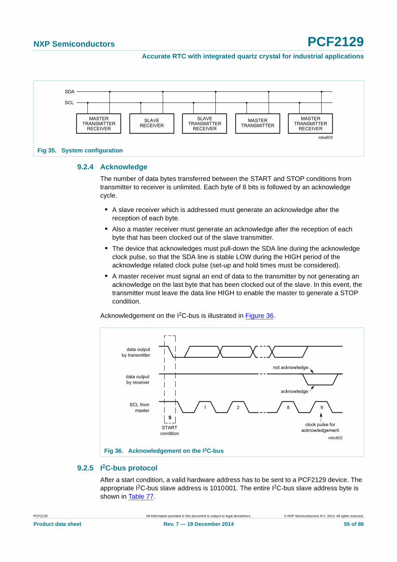
NXP Semiconductors PCF2129Accurate RTC with integrated quartz crystal for industrial applications
9.2.4 Acknowledge
The number of data bytes transferred between the START and STOP conditions from transmitter to receiver is unlimited. Each byte of 8 bits is followed by an acknowledge cycle.
• A slave receiver which is addressed must generate an acknowledge after the reception of each byte.
• Also a master receiver must generate an acknowledge after the reception of each byte that has been clocked out of the slave transmitter.
• The device that acknowledges must pull-down the SDA line during the acknowledge clock pulse, so that the SDA line is stable LOW during the HIGH period of the acknowledge related clock pulse (set-up and hold times must be considered).
• A master receiver must signal an end of data to the transmitter by not generating an acknowledge on the last byte that has been clocked out of the slave. In this event, the transmitter must leave the data line HIGH to enable the master to generate a STOP condition.
Acknowledgement on the I2C-bus is illustrated in Figure 36.
9.2.5 I2C-bus protocol
After a start condition, a valid hardware address has to be sent to a PCF2129 device. The appropriate I2C-bus slave address is 1010001. The entire I2C-bus slave address byte is shown in Table 77.
Fig 35. System configuration
Fig 36. Acknowledgement on the I2C-bus
PCF2129 All information provided in this document is subject to legal disclaimers. © NXP Semiconductors N.V. 2014. All rights reserved.
Product data sheet Rev. 7 — 19 December 2014 55 of 86

NXP Semiconductors PCF2129Accurate RTC with integrated quartz crystal for industrial applications
The R/W bit defines the direction of the following single or multiple byte data transfer (read is logic 1, write is logic 0).
For the format and the timing of the START condition (S), the STOP condition (P), and the acknowledge (A) refer to the I2C-bus specification Ref. 13 “UM10204” and the characteristics table (Table 82). In the write mode, a data transfer is terminated by sending a STOP condition. A repeated START (Sr) condition is not applicable.
9.3 Bus communication and battery backup operation
To save power during battery backup operation (see Section 8.5.1), the bus interfaces are inactive. Therefore the communication via I2C- or SPI-bus should be terminated before the supply of the PCF2129 is switched from VDD to VBAT.
Remark: If the I2C-bus communication was terminated uncontrolled, the I2C-bus has to be reinitialized by sending a STOP followed by a START after the device switched back from battery backup operation to VDD supply operation.
Table 77. I2C slave address byte
Slave address
Bit 7 6 5 4 3 2 1 0
MSB LSB
1 0 1 0 0 0 1 R/W
Fig 37. Bus protocol, writing to registers
Fig 38. Bus protocol, reading from registers
PCF2129 All information provided in this document is subject to legal disclaimers. © NXP Semiconductors N.V. 2014. All rights reserved.
Product data sheet Rev. 7 — 19 December 2014 56 of 86

NXP Semiconductors PCF2129Accurate RTC with integrated quartz crystal for industrial applications
10. Internal circuitry
11. Safety notes
Fig 39. Device diode protection diagram of PCF2129
CAUTION
This device is sensitive to ElectroStatic Discharge (ESD). Observe precautions for handling electrostatic sensitive devices.
Such precautions are described in the ANSI/ESD S20.20, IEC/ST 61340-5, JESD625-A or equivalent standards.
PCF2129 All information provided in this document is subject to legal disclaimers. © NXP Semiconductors N.V. 2014. All rights reserved.
Product data sheet Rev. 7 — 19 December 2014 57 of 86

NXP Semiconductors PCF2129Accurate RTC with integrated quartz crystal for industrial applications
12. Limiting values
[1] Pass level; Human Body Model (HBM) according to Ref. 7 “JESD22-A114”.
[2] Pass level; Charged-Device Model (CDM), according to Ref. 8 “JESD22-C101”.
[3] Pass level; latch-up testing according to Ref. 9 “JESD78” at maximum ambient temperature (Tamb(max)).
[4] According to the store and transport requirements (see Ref. 14 “UM10569”) the devices have to be stored at a temperature of +8 C to +45 C and a humidity of 25 % to 75 %.
Table 78. Limiting valuesIn accordance with the Absolute Maximum Rating System (IEC 60134).
Symbol Parameter Conditions Min Max Unit
VDD supply voltage 0.5 +6.5 V
IDD supply current 50 +50 mA
Vi input voltage 0.5 +6.5 V
II input current 10 +10 mA
VO output voltage 0.5 +6.5 V
IO output current 10 +10 mA
at pin SDA/CE 10 +20 mA
VBAT battery supply voltage 0.5 +6.5 V
Ptot total power dissipation - 300 mW
VESD electrostatic discharge voltage
HBM [1] - 4000 V
CDM [2] - 1250 V
Ilu latch-up current [3] - 200 mA
Tstg storage temperature [4] 55 +85 C
Tamb ambient temperature operating device 40 +85 C
PCF2129 All information provided in this document is subject to legal disclaimers. © NXP Semiconductors N.V. 2014. All rights reserved.
Product data sheet Rev. 7 — 19 December 2014 58 of 86

NXP Semiconductors PCF2129Accurate RTC with integrated quartz crystal for industrial applications
13. Static characteristics
Table 79. Static characteristicsVDD = 1.8 V to 4.2 V; VSS = 0 V; Tamb = 40 C to +85 C, unless otherwise specified.
Symbol Parameter Conditions Min Typ Max Unit
Supplies
VDD supply voltage [1] 1.8 - 4.2 V
VBAT battery supply voltage 1.8 - 4.2 V
VDD(cal) calibration supply voltage - 3.3 - V
Vlow low voltage - 1.2 - V
IDD supply current interface active;supplied by VDD
SPI-bus (fSCL = 6.5 MHz) - - 800 A
I2C-bus (fSCL = 400 kHz) - - 200 A
interface inactive (fSCL = 0 Hz)[2]; TCR[1:0] = 00 (see Table 13 on page 12)
PWRMNG[2:0] = 111 (see Table 19 on page 16);TSOFF = 1 (see Table 58 on page 41);COF[2:0] = 111 (see Table 15 on page 14)
VDD = 1.8 V - 470 - nA
VDD = 3.3 V - 700 1500 nA
VDD = 4.2 V - 800 - nA
PWRMNG[2:0] = 111 (see Table 19 on page 16);TSOFF = 1 (see Table 58 on page 41);COF[2:0] = 000 (see Table 15 on page 14)
VDD = 1.8 V - 560 - nA
VDD = 3.3 V - 850 - nA
VDD = 4.2 V - 1050 - nA
PWRMNG[2:0] = 000 (see Table 19 on page 16);TSOFF = 0 (see Table 58 on page 41);COF[2:0] = 111 (see Table 15 on page 14)
VDD or VBAT = 1.8 V [3] - 1750 - nA
VDD or VBAT = 3.3 V [3] - 2150 - nA
VDD or VBAT = 4.2 V [3] - 2350 3500 nA
PWRMNG[2:0] = 000 (see Table 19 on page 16);TSOFF = 0 (see Table 58 on page 41);COF[2:0] = 000 (see Table 15 on page 14)
VDD or VBAT = 1.8 V [3] - 1840 - nA
VDD or VBAT = 3.3 V [3] - 2300 - nA
VDD or VBAT = 4.2 V [3] - 2600 - nA
IL(bat) battery leakage current VDD is active supply;VBAT = 3.0 V
- 50 100 nA
PCF2129 All information provided in this document is subject to legal disclaimers. © NXP Semiconductors N.V. 2014. All rights reserved.
Product data sheet Rev. 7 — 19 December 2014 59 of 86
NXP Semiconductors PCF2129Accurate RTC with integrated quartz crystal for industrial applications
[1] For reliable oscillator start-up at power-on: VDD(po)min = VDD(min) + 0.3 V.
[2] Timer source clock = 1⁄60 Hz, level of pins SDA/CE, SDI, and SCL is VDD or VSS.
[3] When the device is supplied by the VBAT pin instead of the VDD pin, the current values for IBAT are as specified for IDD under the same conditions.
[4] The I2C-bus and SPI-bus interfaces of PCF2129 are 5 V tolerant.
[5] Tested on sample basis.
[6] For further information, see Figure 40.
Power management
Vth(sw)bat battery switch threshold voltage
- 2.5 - V
Vth(bat)low low battery threshold voltage
- 2.5 - V
Tamb = 25 C 2.25 - 2.85 V
Inputs[4]
VI input voltage 0.5 - VDD + 0.5 V
VIL LOW-level input voltage - - 0.25VDD V
Tamb = 20 C to +85 C;VDD > 2.0 V
- - 0.3VDD V
VIH HIGH-level input voltage 0.7VDD - - V
ILI input leakage current VI = VDD or VSS - 0 - A
post ESD event 1 - +1 A
Ci input capacitance [5] - - 7 pF
Outputs
VO output voltage on pins CLKOUT, INT, referring to external pull-up
0.5 - +5.5 V
on pin BBS 1.8 - 4.2 V
on pin SDO 0.5 - VDD + 0.5 V
VOH HIGH output voltage on pin SDO 0.8VDD - VDD V
VOL LOW output voltage on pins CLKOUT, INT, and SDO
VSS - 0.2VDD V
IOL LOW-level output current output sink current;VOL = 0.4 V
on pin SDA/CE [6] 3 17 - mA
on all other outputs 1.0 - - mA
IOH HIGH-level output current output source current;on pin SDO;VOH = 3.8 V;VDD = 4.2 V
1.0 - - mA
ILO output leakage current VO = VDD or VSS - 0 - A
post ESD event 1 - +1 A
Table 79. Static characteristics …continuedVDD = 1.8 V to 4.2 V; VSS = 0 V; Tamb = 40 C to +85 C, unless otherwise specified.
Symbol Parameter Conditions Min Typ Max Unit
PCF2129 All information provided in this document is subject to legal disclaimers. © NXP Semiconductors N.V. 2014. All rights reserved.
Product data sheet Rev. 7 — 19 December 2014 60 of 86

NXP Semiconductors PCF2129Accurate RTC with integrated quartz crystal for industrial applications
13.1 Current consumption characteristics, typical
Typical value; VOL = 0.4 V.
Fig 40. IOL on pin SDA/CE
CLKOUT disabled; PWRMNG[2:0] = 111; TSOFF = 1; TS input floating.
Fig 41. IDD as a function of temperature
PCF2129 All information provided in this document is subject to legal disclaimers. © NXP Semiconductors N.V. 2014. All rights reserved.
Product data sheet Rev. 7 — 19 December 2014 61 of 86

NXP Semiconductors PCF2129Accurate RTC with integrated quartz crystal for industrial applications
a. PWRMNG[2:0] = 111; TSOFF = 1; Tamb = 25 C; TS input floating
b. PWRMNG[2:0] = 000; TSOFF = 0; Tamb = 25 C; TS input floating
Fig 42. IDD as a function of VDD
PCF2129 All information provided in this document is subject to legal disclaimers. © NXP Semiconductors N.V. 2014. All rights reserved.
Product data sheet Rev. 7 — 19 December 2014 62 of 86

NXP Semiconductors PCF2129Accurate RTC with integrated quartz crystal for industrial applications
Interface inactive; Tamb = 25 C; VBAT = 0 V; default configuration.
Description of the PWRMNG[2:0] settings, see Table 19 on page 16.
(1) VDD = 1.8 V.
(2) VDD = 3.3 V.
(3) VDD = 4.2 V.
(4) VDD or VBAT = 1.8 V.
(5) VDD or VBAT = 3.3 V.
(6) VDD or VBAT = 4.2 V.
Fig 43. Typical IDD as a function of the power management settings
PCF2129 All information provided in this document is subject to legal disclaimers. © NXP Semiconductors N.V. 2014. All rights reserved.
Product data sheet Rev. 7 — 19 December 2014 63 of 86

NXP Semiconductors PCF2129Accurate RTC with integrated quartz crystal for industrial applications
13.2 Frequency characteristics
[1] 1 ppm corresponds to a time deviation of 0.0864 seconds per day.
[2] Only valid if CLKOUT frequencies are not equal to 32.768 kHz or if CLKOUT is disabled.
[3] Not production tested. Effects of reflow soldering are included (see Ref. 3 “AN11186”).
Table 80. Frequency characteristicsVDD = 1.8 V to 4.2 V; VSS = 0 V; Tamb = +25 C, unless otherwise specified.
Symbol Parameter Conditions Min Typ Max Unit
fo output frequency on pin CLKOUT;VDD or VBAT = 3.3 V;COF[2:0] = 000;AO[3:0] = 1000
- 32.768 - kHz
f/f frequency stability VDD or VBAT = 3.3 V
PCF2129AT
Tamb = 15 C to +60 C [1][2] - 3 5 ppm
Tamb = 25 C to 15 C and Tamb = +60 C to +65 C
[1][2] - 5 10 ppm
PCF2129T
Tamb = 30 C to +80 C [1][2] - 3 8 ppm
Tamb = 40 C to 30 C and Tamb = +80 C to +85 C
[1][2] - 5 15 ppm
fxtal/fxtal relative crystal frequency variation
crystal aging
PCF2129AT
first year;VDD or VBAT = 3.3 V
[3] - - 3 ppm
PCF2129T
first year [3] - - 3 ppm
ten years - - 8 ppm
f/V frequency variation with voltage
on pin CLKOUT - 1 - ppm/V
PCF2129 All information provided in this document is subject to legal disclaimers. © NXP Semiconductors N.V. 2014. All rights reserved.
Product data sheet Rev. 7 — 19 December 2014 64 of 86

NXP Semiconductors PCF2129Accurate RTC with integrated quartz crystal for industrial applications
(1) Typical temperature compensated frequency response.
(2) Uncompensated typical tuning-fork crystal frequency.
Fig 44. Typical characteristic of frequency with respect to temperature of PCF2129AT
(1) Typical temperature compensated frequency response.
(2) Uncompensated typical tuning-fork crystal frequency.
Fig 45. Typical characteristic of frequency with respect to temperature of PCF2129T
PCF2129 All information provided in this document is subject to legal disclaimers. © NXP Semiconductors N.V. 2014. All rights reserved.
Product data sheet Rev. 7 — 19 December 2014 65 of 86

NXP Semiconductors PCF2129Accurate RTC with integrated quartz crystal for industrial applications
14. Dynamic characteristics
14.1 SPI-bus timing characteristics
[1] No load value; bus is held up by bus capacitance; use RC time constant with application values.
Table 81. SPI-bus characteristicsVDD = 1.8 V to 4.2 V; VSS = 0 V; Tamb = 40 C to +85 C, unless otherwise specified. All timing values are valid within the operating supply voltage at ambient temperature and referenced to VIL and VIH with an input voltage swing of VSS to VDD (see Figure 46).
Symbol Parameter Conditions VDD = 1.8 V VDD = 4.2 V Unit
Min Max Min Max
Pin SCL
fclk(SCL) SCL clock frequency - 2.0 - 6.5 MHz
tSCL SCL time 800 - 140 - ns
tclk(H) clock HIGH time 100 - 70 - ns
tclk(L) clock LOW time 400 - 70 - ns
tr rise time for SCL signal - 100 - 100 ns
tf fall time for SCL signal - 100 - 100 ns
Pin SDA/CE
tsu(CE_N) CE_N set-up time 60 - 30 - ns
th(CE_N) CE_N hold time 40 - 25 - ns
trec(CE_N) CE_N recovery time 100 - 30 - ns
tw(CE_N) CE_N pulse width - 0.99 - 0.99 s
Pin SDI
tsu set-up time set-up time for SDI data 70 - 20 - ns
th hold time hold time for SDI data 70 - 20 - ns
Pin SDO
td(R)SDO SDO read delay time CL = 50 pF - 225 - 55 ns
tdis(SDO) SDO disable time [1] - 90 - 25 ns
tt(SDI-SDO) transition time from SDI to SDO
to avoid bus conflict 0 - 0 - ns
PCF2129 All information provided in this document is subject to legal disclaimers. © NXP Semiconductors N.V. 2014. All rights reserved.
Product data sheet Rev. 7 — 19 December 2014 66 of 86

NXP Semiconductors PCF2129Accurate RTC with integrated quartz crystal for industrial applications
Fig 46. SPI-bus timing
PCF2129 All information provided in this document is subject to legal disclaimers. © NXP Semiconductors N.V. 2014. All rights reserved.
Product data sheet Rev. 7 — 19 December 2014 67 of 86

NXP Semiconductors PCF2129Accurate RTC with integrated quartz crystal for industrial applications
14.2 I2C-bus timing characteristics
[1] The minimum SCL clock frequency is limited by the bus time-out feature which resets the serial bus interface if either the SDA or SCL is held LOW for a minimum of 25 ms. The bus time-out feature must be disabled for DC operation.
[2] A master device must internally provide a hold time of at least 300 ns for the SDA signal (refer to the VIL of the SCL signal) in order to bridge the undefined region of the falling edge of SCL.
[3] Cb is the total capacitance of one bus line in pF.
[4] The maximum tf for the SDA and SCL bus lines is 300 ns. The maximum fall time for the SDA output stage, tf is 250 ns. This allows series protection resistors to be connected between the SDA/CE pin, the SCL pin, and the SDA/SCL bus lines without exceeding the maximum tf.
[5] tVD;ACK is the time of the acknowledgement signal from SCL LOW to SDA (out) LOW.
[6] tVD;DAT is the minimum time for valid SDA (out) data following SCL LOW.
[7] Input filters on the SDA and SCL inputs suppress noise spikes of less than 50 ns.
Table 82. I2C-bus characteristicsAll timing characteristics are valid within the operating supply voltage and ambient temperature range and reference to 30 % and 70 % with an input voltage swing of VSS to VDD (see Figure 47).
Symbol Parameter Standard mode Fast-mode (Fm) Unit
Min Max Min Max
Pin SCL
fSCL SCL clock frequency [1] 0 100 0 400 kHz
tLOW LOW period of the SCL clock 4.7 - 1.3 - s
tHIGH HIGH period of the SCL clock 4.0 - 0.6 - s
Pin SDA/CE
tSU;DAT data set-up time 250 - 100 - ns
tHD;DAT data hold time 0 - 0 - ns
Pins SCL and SDA/CE
tBUF bus free time between a STOP and START condition
4.7 - 1.3 - s
tSU;STO set-up time for STOP condition 4.0 - 0.6 - s
tHD;STA hold time (repeated) START condition
4.0 - 0.6 - s
tSU;STA set-up time for a repeated START condition
4.7 - 0.6 - s
tr rise time of both SDA and SCL signals
[2][3][4] - 1000 20 + 0.1Cb 300 ns
tf fall time of both SDA and SCL signals
[2][3][4] - 300 20 + 0.1Cb 300 ns
tVD;ACK data valid acknowledge time [5] 0.1 3.45 0.1 0.9 s
tVD;DAT data valid time [6] 300 - 75 - ns
tSP pulse width of spikes that must be suppressed by the input filter
[7] - 50 - 50 ns
PCF2129 All information provided in this document is subject to legal disclaimers. © NXP Semiconductors N.V. 2014. All rights reserved.
Product data sheet Rev. 7 — 19 December 2014 68 of 86

NXP Semiconductors PCF2129Accurate RTC with integrated quartz crystal for industrial applications
Fig 47. I2C-bus timing diagram; rise and fall times refer to 30 % and 70 %
PCF2129 All information provided in this document is subject to legal disclaimers. © NXP Semiconductors N.V. 2014. All rights reserved.
Product data sheet Rev. 7 — 19 December 2014 69 of 86

NXP Semiconductors PCF2129Accurate RTC with integrated quartz crystal for industrial applications
15. Application information
For information about application configuration, see Ref. 3 “AN11186”.
Ci: In case mechanical switches are used, a capacitor of 1 nF is recommended.
RPU: For example, 10 k.
Fig 48. General application diagram
PCF2129 All information provided in this document is subject to legal disclaimers. © NXP Semiconductors N.V. 2014. All rights reserved.
Product data sheet Rev. 7 — 19 December 2014 70 of 86

NXP Semiconductors PCF2129Accurate RTC with integrated quartz crystal for industrial applications
16. Package outline
Fig 49. Package outline SOT163-1 (SO20) of PCF2129AT
PCF2129 All information provided in this document is subject to legal disclaimers. © NXP Semiconductors N.V. 2014. All rights reserved.
Product data sheet Rev. 7 — 19 December 2014 71 of 86

NXP Semiconductors PCF2129Accurate RTC with integrated quartz crystal for industrial applications
Fig 50. Package outline SOT162-1 (SO16) of PCF2129T
PCF2129 All information provided in this document is subject to legal disclaimers. © NXP Semiconductors N.V. 2014. All rights reserved.
Product data sheet Rev. 7 — 19 December 2014 72 of 86

NXP Semiconductors PCF2129Accurate RTC with integrated quartz crystal for industrial applications
17. Packing information
17.1 Tape and reel information
For tape and reel packing information, see
• Ref. 11 “SOT162-1_518” on page 78 for the PCF2129T.
• Ref. 12 “SOT163-1_518” on page 78 for the PCF2129AT.
18. Soldering
For information about soldering, see Ref. 3 “AN11186”.
18.1 Footprint information
Fig 51. Footprint information for reflow soldering of SOT163-1 (SO20) of PCF2129AT
PCF2129 All information provided in this document is subject to legal disclaimers. © NXP Semiconductors N.V. 2014. All rights reserved.
Product data sheet Rev. 7 — 19 December 2014 73 of 86

NXP Semiconductors PCF2129Accurate RTC with integrated quartz crystal for industrial applications
Fig 52. Footprint information for reflow soldering of SOT162-1 (SO16) of PCF2129T
PCF2129 All information provided in this document is subject to legal disclaimers. © NXP Semiconductors N.V. 2014. All rights reserved.
Product data sheet Rev. 7 — 19 December 2014 74 of 86
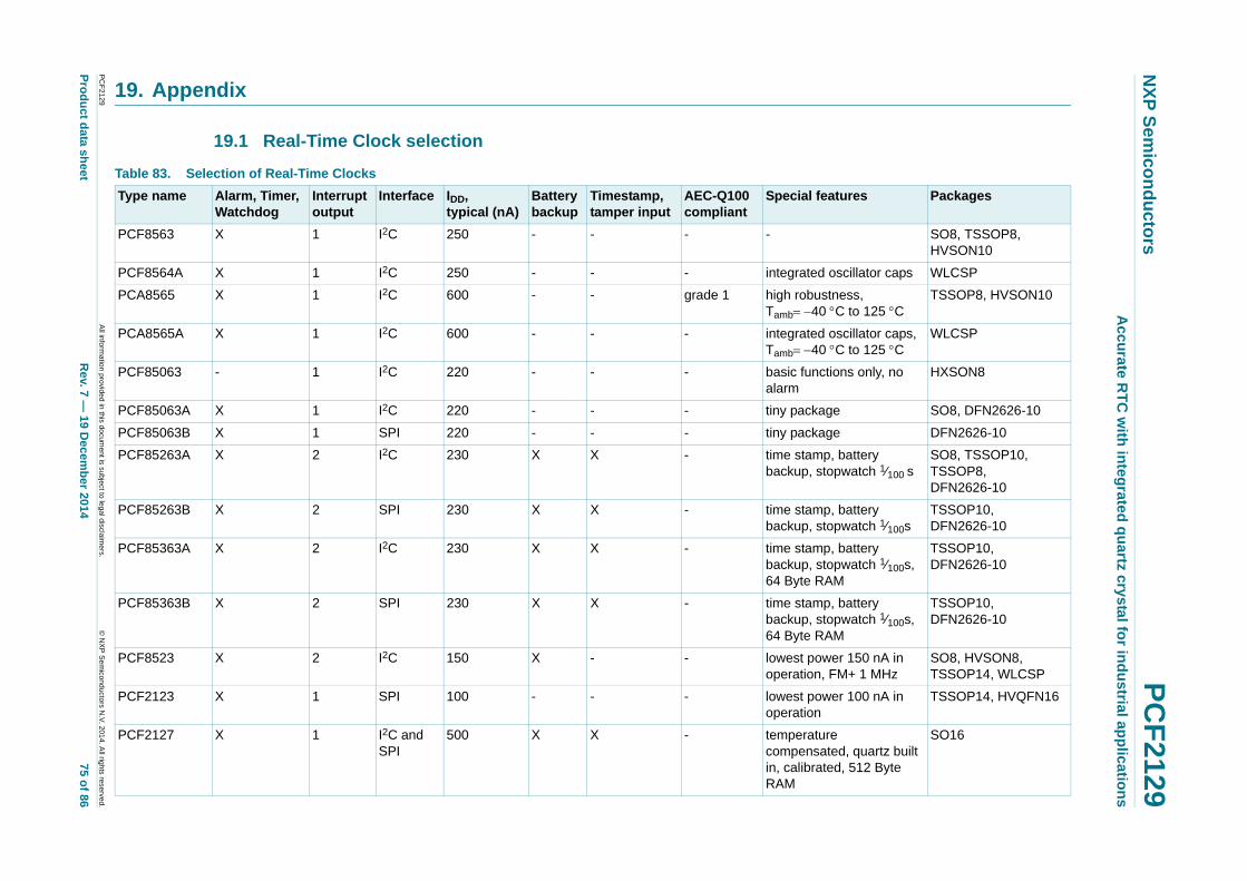
xxxxxxxxxxxxxxxxxxxxx xxxxxxxxxxxxxxxxxxxxxxxxxx xxxxxxx x x x xxxxxxxxxxxxxxxxxxxxxxxxxxxxxx xxxxxxxxxxxxxxxxxxx xx xx xxxxx xxxxxxxxxxxxxxxxxxxxxxxxxxx xxxxxxxxxxxxxxxxxxx xxxxxx xxxxxxxxxxxxxxxxxxxxxxxxxxxxxxxxxxx xxxxxxxxxxxx x x xxxxxxxxxxxxxxxxxxxxx xxxxxxxxxxxxxxxxxxxxxxxxxxxxxx xxxxx xxxxxxxxxxxxxxxxxxxxxxxxxxxxxxxxxxxxxxxxxxxxxxxxxx xxxxxxxx xxxxxxxxxxxxxxxxxxxxxxxxx xxxxxxxxxxxxxxxxxxxx xxx
PC
F21
29
Pro
du
ct data sh
NX
P S
emico
nd
ucto
rsP
CF
2129A
cc
ura
te R
TC
with
inte
gra
ted
qu
artz cry
sta
l for in
du
strial a
pp
licatio
ns
19. Appendix
19.1 Real-Time Clock selection
atures Packages
SO8, TSSOP8, HVSON10
oscillator caps WLCSP
stness,C to 125 C
TSSOP8, HVSON10
oscillator caps,C to 125 C
WLCSP
tions only, no HXSON8
ge SO8, DFN2626-10
ge DFN2626-10
p, battery topwatch 1⁄100 s
SO8, TSSOP10, TSSOP8, DFN2626-10
p, battery topwatch 1⁄100s
TSSOP10, DFN2626-10
p, battery topwatch 1⁄100s, AM
TSSOP10, DFN2626-10
p, battery topwatch 1⁄100s, AM
TSSOP10, DFN2626-10
wer 150 nA in , FM+ 1 MHz
SO8, HVSON8, TSSOP14, WLCSP
wer 100 nA in TSSOP14, HVQFN16
re ted, quartz built
ted, 512 Byte
SO16
All inform
ation provided
in this docum
ent is subject to leg
al disclaim
ers.©
NX
P S
em
iconductors N
.V. 2014. A
ll rights reserved.
eetR
ev. 7 — 19 D
ecemb
er 2014
75 of 86
Table 83. Selection of Real-Time Clocks
Type name Alarm, Timer,Watchdog
Interruptoutput
Interface IDD,typical (nA)
Batterybackup
Timestamp,tamper input
AEC-Q100compliant
Special fe
PCF8563 X 1 I2C 250 - - - -
PCF8564A X 1 I2C 250 - - - integrated
PCA8565 X 1 I2C 600 - - grade 1 high robuTamb40
PCA8565A X 1 I2C 600 - - - integratedTamb40
PCF85063 - 1 I2C 220 - - - basic funcalarm
PCF85063A X 1 I2C 220 - - - tiny packa
PCF85063B X 1 SPI 220 - - - tiny packa
PCF85263A X 2 I2C 230 X X - time stambackup, s
PCF85263B X 2 SPI 230 X X - time stambackup, s
PCF85363A X 2 I2C 230 X X - time stambackup, s64 Byte R
PCF85363B X 2 SPI 230 X X - time stambackup, s64 Byte R
PCF8523 X 2 I2C 150 X - - lowest pooperation
PCF2123 X 1 SPI 100 - - - lowest pooperation
PCF2127 X 1 I2C and SPI
500 X X - temperatucompensain, calibraRAM

xxxxxxxxxxxxxxxxxxxxx xxxxxxxxxxxxxxxxxxxxxxxxxx xxxxxxx x x x xxxxxxxxxxxxxxxxxxxxxxxxxxxxxx xxxxxxxxxxxxxxxxxxx xx xx xxxxx xxxxxxxxxxxxxxxxxxxxxxxxxxx xxxxxxxxxxxxxxxxxxx xxxxxx xxxxxxxxxxxxxxxxxxxxxxxxxxxxxxxxxxx xxxxxxxxxxxx x x xxxxxxxxxxxxxxxxxxxxx xxxxxxxxxxxxxxxxxxxxxxxxxxxxxx xxxxx xxxxxxxxxxxxxxxxxxxxxxxxxxxxxxxxxxxxxxxxxxxxxxxxxx xxxxxxxx xxxxxxxxxxxxxxxxxxxxxxxxx xxxxxxxxxxxxxxxxxxxx xxx
PC
F21
29
Pro
du
ct data sh
NX
P S
emico
nd
ucto
rsP
CF
2129A
cc
ura
te R
TC
with
inte
gra
ted
qu
artz cry
sta
l for in
du
strial a
pp
licatio
ns
PCF2127A X 1 I2C and SPI
500 X X - temperature compensated, quartz built
ted, 512 Byte
SO20
re ted, quartz built
ted
SO16
re ted, quartz built
ted
SO20
re ted, quartz built
ted
SO16
stness,C to 125 C
TSSOP14
Table 83. Selection of Real-Time Clocks …continued
Type name Alarm, Timer,Watchdog
Interruptoutput
Interface IDD,typical (nA)
Batterybackup
Timestamp,tamper input
AEC-Q100compliant
Special features Packages
All inform
ation provided
in this docum
ent is subject to leg
al disclaim
ers.©
NX
P S
em
iconductors N
.V. 2014. A
ll rights reserved.
eetR
ev. 7 — 19 D
ecemb
er 2014
76 of 86
in, calibraRAM
PCF2129 X 1 I2C and SPI
500 X X - temperatucompensain, calibra
PCF2129A X 1 I2C and SPI
500 X X - temperatucompensain, calibra
PCA2129 X 1 I2C and SPI
500 X X grade 3 temperatucompensain, calibra
PCA21125 X 1 SPI 820 - - grade 1 high robuTamb40

NXP Semiconductors PCF2129Accurate RTC with integrated quartz crystal for industrial applications
20. Abbreviations
Table 84. Abbreviations
Acronym Description
AM Ante Meridiem
BCD Binary Coded Decimal
CDM Charged Device Model
CMOS Complementary Metal-Oxide Semiconductor
DC Direct Current
GPS Global Positioning System
HBM Human Body Model
I2C Inter-Integrated Circuit
IC Integrated Circuit
LSB Least Significant Bit
MCU Microcontroller Unit
MM Machine Model
MSB Most Significant Bit
PM Post Meridiem
POR Power-On Reset
PORO Power-On Reset Override
PPM Parts Per Million
RC Resistance-Capacitance
RTC Real-Time Clock
SCL Serial CLock line
SDA Serial DAta line
SPI Serial Peripheral Interface
SRAM Static Random Access Memory
TCXO Temperature Compensated Xtal Oscillator
Xtal crystal
PCF2129 All information provided in this document is subject to legal disclaimers. © NXP Semiconductors N.V. 2014. All rights reserved.
Product data sheet Rev. 7 — 19 December 2014 77 of 86
NXP Semiconductors PCF2129Accurate RTC with integrated quartz crystal for industrial applications
21. References
[1] AN10365 — Surface mount reflow soldering description
[2] AN10853 — Handling precautions of ESD sensitive devices
[3] AN11186 — Application and soldering information for the PCA2129 and PCF2129 TCXO RTC
[4] IEC 60134 — Rating systems for electronic tubes and valves and analogous semiconductor devices
[5] IEC 61340-5 — Protection of electronic devices from electrostatic phenomena
[6] IPC/JEDEC J-STD-020D — Moisture/Reflow Sensitivity Classification for Nonhermetic Solid State Surface Mount Devices
[7] JESD22-A114 — Electrostatic Discharge (ESD) Sensitivity Testing Human Body Model (HBM)
[8] JESD22-C101 — Field-Induced Charged-Device Model Test Method for Electrostatic-Discharge-Withstand Thresholds of Microelectronic Components
[9] JESD78 — IC Latch-Up Test
[10] JESD625-A — Requirements for Handling Electrostatic-Discharge-Sensitive (ESDS) Devices
[11] SOT162-1_518 — SO16; Reel pack; SMD, 13”, packing information
[12] SOT163-1_518 — SO20; Reel pack; SMD, 13”, packing information
[13] UM10204 — I2C-bus specification and user manual
[14] UM10569 — Store and transport requirements
[15] UM10762 — User manual for the accurate RTC demo board OM13513 containing PCF2127T and PCF2129AT
PCF2129 All information provided in this document is subject to legal disclaimers. © NXP Semiconductors N.V. 2014. All rights reserved.
Product data sheet Rev. 7 — 19 December 2014 78 of 86

NXP Semiconductors PCF2129Accurate RTC with integrated quartz crystal for industrial applications
22. Revision history
Table 85. Revision history
Document ID Release date Data sheet status Change notice Supersedes
PCF2129 v.7 20141219 Product data sheet - PCF2129AT v.6PCF2129T v.4
Modifications: • The format of this data sheet has been redesigned to comply with the new identity guidelines of NXP Semiconductors.
• Legal texts have been adapted to the new company name where appropriate.
• Combined PCF2129AT and PCF2129T data sheets to one data sheet
• Added Figure 4, Figure 43 and Figure 48
• Enhanced Figure 8, Figure 12, Figure 20, Section 8.11.1, Figure 37, Figure 38
• Added Section 9.3
• Changed IDD values in Table 79
• Added VOH and VOL values in Table 79
• Enhanced description of internal operating voltage
• Added register bit allocation tables
• Enhanced ESD HBM values
• Fixed typos
PCF2129AT
PCF2127AT v.6 20130711 Product data sheet - PCF2127AT v.5
PCF2129AT v.5 20130212 Product data sheet - PCF2129AT v.4
PCF2129AT v.4 20121107 Product data sheet - PCF2129AT v.3
PCF2129AT v.3 20121004 Product data sheet - PCF2129AT v.2
PCF2129AT v.2 20100507 Product data sheet - PCF2129AT v.1
PCF2129AT v.1 20100113 Product data sheet - -
PCF2129T
PCF2129T v.4 20130711 Product data sheet - PCF2129T v.3
PCF2129T v.3 20130212 Product data sheet - PCF2129T v.2
PCF2129T v.2 20121025 Product data sheet - PCF2129T v.1
PCF2129T v.1 20120618 Product data sheet - -
PCF2129 All information provided in this document is subject to legal disclaimers. © NXP Semiconductors N.V. 2014. All rights reserved.
Product data sheet Rev. 7 — 19 December 2014 79 of 86
NXP Semiconductors PCF2129Accurate RTC with integrated quartz crystal for industrial applications
23. Legal information
23.1 Data sheet status
[1] Please consult the most recently issued document before initiating or completing a design.
[2] The term ‘short data sheet’ is explained in section “Definitions”.
[3] The product status of device(s) described in this document may have changed since this document was published and may differ in case of multiple devices. The latest product status information is available on the Internet at URL http://www.nxp.com.
23.2 Definitions
Draft — The document is a draft version only. The content is still under internal review and subject to formal approval, which may result in modifications or additions. NXP Semiconductors does not give any representations or warranties as to the accuracy or completeness of information included herein and shall have no liability for the consequences of use of such information.
Short data sheet — A short data sheet is an extract from a full data sheet with the same product type number(s) and title. A short data sheet is intended for quick reference only and should not be relied upon to contain detailed and full information. For detailed and full information see the relevant full data sheet, which is available on request via the local NXP Semiconductors sales office. In case of any inconsistency or conflict with the short data sheet, the full data sheet shall prevail.
Product specification — The information and data provided in a Product data sheet shall define the specification of the product as agreed between NXP Semiconductors and its customer, unless NXP Semiconductors and customer have explicitly agreed otherwise in writing. In no event however, shall an agreement be valid in which the NXP Semiconductors product is deemed to offer functions and qualities beyond those described in the Product data sheet.
23.3 Disclaimers
Limited warranty and liability — Information in this document is believed to be accurate and reliable. However, NXP Semiconductors does not give any representations or warranties, expressed or implied, as to the accuracy or completeness of such information and shall have no liability for the consequences of use of such information. NXP Semiconductors takes no responsibility for the content in this document if provided by an information source outside of NXP Semiconductors.
In no event shall NXP Semiconductors be liable for any indirect, incidental, punitive, special or consequential damages (including - without limitation - lost profits, lost savings, business interruption, costs related to the removal or replacement of any products or rework charges) whether or not such damages are based on tort (including negligence), warranty, breach of contract or any other legal theory.
Notwithstanding any damages that customer might incur for any reason whatsoever, NXP Semiconductors’ aggregate and cumulative liability towards customer for the products described herein shall be limited in accordance with the Terms and conditions of commercial sale of NXP Semiconductors.
Right to make changes — NXP Semiconductors reserves the right to make changes to information published in this document, including without limitation specifications and product descriptions, at any time and without notice. This document supersedes and replaces all information supplied prior to the publication hereof.
Suitability for use — NXP Semiconductors products are not designed, authorized or warranted to be suitable for use in life support, life-critical or safety-critical systems or equipment, nor in applications where failure or malfunction of an NXP Semiconductors product can reasonably be expected to result in personal injury, death or severe property or environmental damage. NXP Semiconductors and its suppliers accept no liability for inclusion and/or use of NXP Semiconductors products in such equipment or applications and therefore such inclusion and/or use is at the customer’s own risk.
Applications — Applications that are described herein for any of these products are for illustrative purposes only. NXP Semiconductors makes no representation or warranty that such applications will be suitable for the specified use without further testing or modification.
Customers are responsible for the design and operation of their applications and products using NXP Semiconductors products, and NXP Semiconductors accepts no liability for any assistance with applications or customer product design. It is customer’s sole responsibility to determine whether the NXP Semiconductors product is suitable and fit for the customer’s applications and products planned, as well as for the planned application and use of customer’s third party customer(s). Customers should provide appropriate design and operating safeguards to minimize the risks associated with their applications and products.
NXP Semiconductors does not accept any liability related to any default, damage, costs or problem which is based on any weakness or default in the customer’s applications or products, or the application or use by customer’s third party customer(s). Customer is responsible for doing all necessary testing for the customer’s applications and products using NXP Semiconductors products in order to avoid a default of the applications and the products or of the application or use by customer’s third party customer(s). NXP does not accept any liability in this respect.
Limiting values — Stress above one or more limiting values (as defined in the Absolute Maximum Ratings System of IEC 60134) will cause permanent damage to the device. Limiting values are stress ratings only and (proper) operation of the device at these or any other conditions above those given in the Recommended operating conditions section (if present) or the Characteristics sections of this document is not warranted. Constant or repeated exposure to limiting values will permanently and irreversibly affect the quality and reliability of the device.
Terms and conditions of commercial sale — NXP Semiconductors products are sold subject to the general terms and conditions of commercial sale, as published at http://www.nxp.com/profile/terms, unless otherwise agreed in a valid written individual agreement. In case an individual agreement is concluded only the terms and conditions of the respective agreement shall apply. NXP Semiconductors hereby expressly objects to applying the customer’s general terms and conditions with regard to the purchase of NXP Semiconductors products by customer.
No offer to sell or license — Nothing in this document may be interpreted or construed as an offer to sell products that is open for acceptance or the grant, conveyance or implication of any license under any copyrights, patents or other industrial or intellectual property rights.
Document status[1][2] Product status[3] Definition
Objective [short] data sheet Development This document contains data from the objective specification for product development.
Preliminary [short] data sheet Qualification This document contains data from the preliminary specification.
Product [short] data sheet Production This document contains the product specification.
PCF2129 All information provided in this document is subject to legal disclaimers. © NXP Semiconductors N.V. 2014. All rights reserved.
Product data sheet Rev. 7 — 19 December 2014 80 of 86
NXP Semiconductors PCF2129Accurate RTC with integrated quartz crystal for industrial applications
Export control — This document as well as the item(s) described herein may be subject to export control regulations. Export might require a prior authorization from competent authorities.
Non-automotive qualified products — Unless this data sheet expressly states that this specific NXP Semiconductors product is automotive qualified, the product is not suitable for automotive use. It is neither qualified nor tested in accordance with automotive testing or application requirements. NXP Semiconductors accepts no liability for inclusion and/or use of non-automotive qualified products in automotive equipment or applications.
In the event that customer uses the product for design-in and use in automotive applications to automotive specifications and standards, customer (a) shall use the product without NXP Semiconductors’ warranty of the product for such automotive applications, use and specifications, and (b) whenever customer uses the product for automotive applications beyond NXP Semiconductors’ specifications such use shall be solely at customer’s
own risk, and (c) customer fully indemnifies NXP Semiconductors for any liability, damages or failed product claims resulting from customer design and use of the product for automotive applications beyond NXP Semiconductors’ standard warranty and NXP Semiconductors’ product specifications.
Translations — A non-English (translated) version of a document is for reference only. The English version shall prevail in case of any discrepancy between the translated and English versions.
23.4 TrademarksNotice: All referenced brands, product names, service names and trademarks are the property of their respective owners.
I2C-bus — logo is a trademark of NXP Semiconductors N.V.
24. Contact information
For more information, please visit: http://www.nxp.com
For sales office addresses, please send an email to: [email protected]
PCF2129 All information provided in this document is subject to legal disclaimers. © NXP Semiconductors N.V. 2014. All rights reserved.
Product data sheet Rev. 7 — 19 December 2014 81 of 86

NXP Semiconductors PCF2129Accurate RTC with integrated quartz crystal for industrial applications
25. Tables
Table 1. Ordering information. . . . . . . . . . . . . . . . . . . . . .2Table 2. Ordering options . . . . . . . . . . . . . . . . . . . . . . . . .2Table 3. Marking codes . . . . . . . . . . . . . . . . . . . . . . . . . .2Table 4. Pin description of PCF2129 . . . . . . . . . . . . . . . .5Table 5. Register overview . . . . . . . . . . . . . . . . . . . . . . .8Table 6. Control_1 - control and status register 1
(address 00h) bit allocation . . . . . . . . . . . . . . .10Table 7. Control_1 - control and status register 1
(address 00h) bit description . . . . . . . . . . . . . .10Table 8. Control_2 - control and status register 2
(address 01h) bit allocation . . . . . . . . . . . . . . . 11Table 9. Control_2 - control and status register 2
(address 01h) bit description . . . . . . . . . . . . . . 11Table 10. Control_3 - control and status register 3
(address 02h) bit allocation . . . . . . . . . . . . . . .12Table 11. Control_3 - control and status register 3
(address 02h) bit description . . . . . . . . . . . . . .12Table 12. CLKOUT_ctl - CLKOUT control register
(address 0Fh) bit allocation . . . . . . . . . . . . . . .12Table 13. CLKOUT_ctl - CLKOUT control register
(address 0Fh) bit description . . . . . . . . . . . . . .12Table 14. Temperature measurement period . . . . . . . . . .13Table 15. CLKOUT frequency selection . . . . . . . . . . . . . .14Table 16. Aging_offset - crystal aging offset register
(address 19h) bit allocation . . . . . . . . . . . . . . .14Table 17. Aging_offset - crystal aging offset register
(address 19h) bit description . . . . . . . . . . . . . .14Table 18. Frequency correction at 25 °C, typical . . . . . . .15Table 19. Power management control bit description. . . .16Table 20. Output pin BBS. . . . . . . . . . . . . . . . . . . . . . . . .21Table 21. Seconds - seconds and clock integrity
register (address 03h) bit allocation . . . . . . . . .25Table 22. Seconds - seconds and clock integrity
register (address 03h) bit description . . . . . . . .25Table 23. Seconds coded in BCD format . . . . . . . . . . . .26Table 24. Minutes - minutes register (address 04h)
bit allocation . . . . . . . . . . . . . . . . . . . . . . . . . . .26Table 25. Minutes - minutes register (address 04h)
bit description . . . . . . . . . . . . . . . . . . . . . . . . . .26Table 26. Hours - hours register (address 05h)
bit allocation . . . . . . . . . . . . . . . . . . . . . . . . . . .27Table 27. Hours - hours register (address 05h)
bit description . . . . . . . . . . . . . . . . . . . . . . . . .27Table 28. Days - days register (address 06h)
bit allocation . . . . . . . . . . . . . . . . . . . . . . . . . . .27Table 29. Days - days register (address 06h)
bit description . . . . . . . . . . . . . . . . . . . . . . . . . .27Table 30. Weekdays - weekdays register (address 07h)
bit allocation . . . . . . . . . . . . . . . . . . . . . . . . . . .28Table 31. Weekdays - weekdays register (address 07h)
bit description . . . . . . . . . . . . . . . . . . . . . . . . . .28Table 32. Weekday assignments . . . . . . . . . . . . . . . . . . .28Table 33. Months - months register (address 08h)
bit allocation . . . . . . . . . . . . . . . . . . . . . . . . . . .29Table 34. Months - months register (address 08h)
bit description . . . . . . . . . . . . . . . . . . . . . . . . . .29
Table 35. Month assignments in BCD format . . . . . . . . . 29Table 36. Years - years register (address 09h)
bit allocation . . . . . . . . . . . . . . . . . . . . . . . . . . 30Table 37. Years - years register (address 09h)
bit description. . . . . . . . . . . . . . . . . . . . . . . . . . 30Table 38. Second_alarm - second alarm register
(address 0Ah) bit allocation . . . . . . . . . . . . . . 33Table 39. Second_alarm - second alarm register
(address 0Ah) bit description . . . . . . . . . . . . . . 33Table 40. Minute_alarm - minute alarm register
(address 0Bh) bit allocation . . . . . . . . . . . . . . 33Table 41. Minute_alarm - minute alarm register
(address 0Bh) bit description . . . . . . . . . . . . . . 33Table 42. Hour_alarm - hour alarm register
(address 0Ch) bit allocation . . . . . . . . . . . . . . 34Table 43. Hour_alarm - hour alarm register
(address 0Ch) bit description . . . . . . . . . . . . . 34Table 44. Day_alarm - day alarm register
(address 0Dh) bit allocation . . . . . . . . . . . . . . 34Table 45. Day_alarm - day alarm register
(address 0Dh) bit description . . . . . . . . . . . . . . 34Table 46. Weekday_alarm - weekday alarm register
(address 0Eh) bit allocation . . . . . . . . . . . . . . 35Table 47. Weekday_alarm - weekday alarm register
(address 0Eh) bit description . . . . . . . . . . . . . . 35Table 48. Watchdg_tim_ctl - watchdog timer control
register (address 10h) bit allocation . . . . . . . . 36Table 49. Watchdg_tim_ctl - watchdog timer control
register (address 10h) bit description . . . . . . . 36Table 50. Watchdg_tim_val - watchdog timer value
register (address 11h) bit allocation . . . . . . . . 36Table 51. Watchdg_tim_val - watchdog timer value
register (address 11h) bit description. . . . . . . . 36Table 52. Programmable watchdog timer . . . . . . . . . . . . 37Table 53. Flag location in register Control_2 . . . . . . . . . . 38Table 54. Example values in register Control_2 . . . . . . . 39Table 55. Example to clear only AF (bit 4). . . . . . . . . . . . 39Table 56. Example to clear only MSF (bit 7) . . . . . . . . . . 39Table 57. Timestp_ctl - timestamp control register
(address 12h) bit allocation . . . . . . . . . . . . . . . 41Table 58. Timestp_ctl - timestamp control register
(address 12h) bit description . . . . . . . . . . . . . . 41Table 59. Sec_timestp - second timestamp register
(address 13h) bit allocation . . . . . . . . . . . . . . . 41Table 60. Sec_timestp - second timestamp register
(address 13h) bit description . . . . . . . . . . . . . . 41Table 61. Min_timestp - minute timestamp register
(address 14h) bit allocation . . . . . . . . . . . . . . . 42Table 62. Min_timestp - minute timestamp register
(address 14h) bit description . . . . . . . . . . . . . . 42Table 63. Hour_timestp - hour timestamp register
(address 15h) bit allocation . . . . . . . . . . . . . . . 42Table 64. Hour_timestp - hour timestamp register
(address 15h) bit description . . . . . . . . . . . . . . 42Table 65. Day_timestp - day timestamp register
(address 16h) bit allocation . . . . . . . . . . . . . . . 43
PCF2129 All information provided in this document is subject to legal disclaimers. © NXP Semiconductors N.V. 2014. All rights reserved.
Product data sheet Rev. 7 — 19 December 2014 82 of 86

NXP Semiconductors PCF2129Accurate RTC with integrated quartz crystal for industrial applications
Table 66. Day_timestp - day timestamp register (address 16h) bit description . . . . . . . . . . . . . .43
Table 67. Mon_timestp - month timestamp register (address 17h) bit allocation . . . . . . . . . . . . . . .43
Table 68. Mon_timestp - month timestamp register (address 17h) bit description . . . . . . . . . . . . . .43
Table 69. Year_timestp - year timestamp register (address 18h) bit allocation . . . . . . . . . . . . . . .43
Table 70. Year_timestp - year timestamp register (address 18h) bit description . . . . . . . . . . . . . .43
Table 71. Battery switch-over and timestamp. . . . . . . . . .44Table 72. Effect of bits MI and SI on pin INT and
bit MSF . . . . . . . . . . . . . . . . . . . . . . . . . . . . . . .46Table 73. First increment of time circuits after
stop release . . . . . . . . . . . . . . . . . . . . . . . . . . .50Table 74. Interface selection input pin IFS . . . . . . . . . . . .51Table 75. Serial interface . . . . . . . . . . . . . . . . . . . . . . . . .52Table 76. Command byte definition . . . . . . . . . . . . . . . . .52Table 77. I2C slave address byte . . . . . . . . . . . . . . . . . . .56Table 78. Limiting values . . . . . . . . . . . . . . . . . . . . . . . . .58Table 79. Static characteristics . . . . . . . . . . . . . . . . . . . .59Table 80. Frequency characteristics . . . . . . . . . . . . . . . .64Table 81. SPI-bus characteristics . . . . . . . . . . . . . . . . . .66Table 82. I2C-bus characteristics . . . . . . . . . . . . . . . . . . .68Table 83. Selection of Real-Time Clocks . . . . . . . . . . . . .75Table 84. Abbreviations . . . . . . . . . . . . . . . . . . . . . . . . . .77Table 85. Revision history . . . . . . . . . . . . . . . . . . . . . . . .79
PCF2129 All information provided in this document is subject to legal disclaimers. © NXP Semiconductors N.V. 2014. All rights reserved.
Product data sheet Rev. 7 — 19 December 2014 83 of 86

NXP Semiconductors PCF2129Accurate RTC with integrated quartz crystal for industrial applications
26. Figures
Fig 1. Block diagram of PCF2129 . . . . . . . . . . . . . . . . . .3Fig 2. Pin configuration for PCF2129AT (SO20) . . . . . . .4Fig 3. Pin configuration for PCF2129T (SO16) . . . . . . . .4Fig 4. Position of the stubs from the package assembly
process . . . . . . . . . . . . . . . . . . . . . . . . . . . . . . . . .4Fig 5. Handling address registers . . . . . . . . . . . . . . . . . .6Fig 6. Battery switch-over behavior in standard mode
with bit BIE set logic 1 (enabled) . . . . . . . . . . . . .18Fig 7. Battery switch-over behavior in direct switching
mode with bit BIE set logic 1 (enabled) . . . . . . . .19Fig 8. Battery switch-over circuit, simplified block
diagram . . . . . . . . . . . . . . . . . . . . . . . . . . . . . . . .20Fig 9. Battery low detection behavior with bit BLIE set
logic 1 (enabled) . . . . . . . . . . . . . . . . . . . . . . . . .21Fig 10. Typical driving capability of VBBS: (VBBS - VDD)
with respect to the output load current IBBS . . . . .22Fig 11. Power failure event due to battery discharge:
reset occurs . . . . . . . . . . . . . . . . . . . . . . . . . . . . .23Fig 12. Dependency between POR and oscillator . . . . . .24Fig 13. Power-On Reset (POR) system. . . . . . . . . . . . . .24Fig 14. Power-On Reset Override (PORO) sequence,
valid for both I2C-bus and SPI-bus . . . . . . . . . . .25Fig 15. Data flow of the time function. . . . . . . . . . . . . . . .30Fig 16. Access time for read/write operations . . . . . . . . .31Fig 17. Alarm function block diagram. . . . . . . . . . . . . . . .32Fig 18. Alarm flag timing diagram . . . . . . . . . . . . . . . . . .35Fig 19. WD_CD set logic 1: watchdog activates an
interrupt when timed out . . . . . . . . . . . . . . . . . . .38Fig 20. Timestamp detection with two push-buttons
on the TS pin (for example, for tamper detection)39Fig 21. Interrupt block diagram . . . . . . . . . . . . . . . . . . . .45Fig 22. INT example for SI and MI when TI_TP
is logic 1. . . . . . . . . . . . . . . . . . . . . . . . . . . . . . . .46Fig 23. INT example for SI and MI when TI_TP
is logic 0. . . . . . . . . . . . . . . . . . . . . . . . . . . . . . . .46Fig 24. Example of shortening the INT pulse by
clearing the MSF flag. . . . . . . . . . . . . . . . . . . . . .47Fig 25. AF timing diagram . . . . . . . . . . . . . . . . . . . . . . . .48Fig 26. STOP bit functional diagram . . . . . . . . . . . . . . . .49Fig 27. STOP bit release timing . . . . . . . . . . . . . . . . . . . .50Fig 28. Interface selection . . . . . . . . . . . . . . . . . . . . . . . .51Fig 29. SDI, SDO configurations . . . . . . . . . . . . . . . . . . .51Fig 30. Data transfer overview. . . . . . . . . . . . . . . . . . . . .52Fig 31. SPI-bus write example. . . . . . . . . . . . . . . . . . . . .53Fig 32. SPI-bus read example . . . . . . . . . . . . . . . . . . . . .53Fig 33. Bit transfer . . . . . . . . . . . . . . . . . . . . . . . . . . . . . .54Fig 34. Definition of START and STOP conditions. . . . . .54Fig 35. System configuration . . . . . . . . . . . . . . . . . . . . . .55Fig 36. Acknowledgement on the I2C-bus . . . . . . . . . . . .55Fig 37. Bus protocol, writing to registers . . . . . . . . . . . . .56Fig 38. Bus protocol, reading from registers . . . . . . . . . .56Fig 39. Device diode protection diagram of PCF2129 . . .57Fig 40. IOL on pin SDA/CE . . . . . . . . . . . . . . . . . . . . . . . .61Fig 41. IDD as a function of temperature . . . . . . . . . . . . .61Fig 42. IDD as a function of VDD . . . . . . . . . . . . . . . . . . . .62Fig 43. Typical IDD as a function of the power
management settings . . . . . . . . . . . . . . . . . . . . . 63Fig 44. Typical characteristic of frequency with respect to
temperature of PCF2129AT . . . . . . . . . . . . . . . . 65Fig 45. Typical characteristic of frequency with respect to
temperature of PCF2129T . . . . . . . . . . . . . . . . . 65Fig 46. SPI-bus timing. . . . . . . . . . . . . . . . . . . . . . . . . . . 67Fig 47. I2C-bus timing diagram; rise and fall times refer to
30 % and 70 % . . . . . . . . . . . . . . . . . . . . . . . . . . 69Fig 48. General application diagram . . . . . . . . . . . . . . . . 70Fig 49. Package outline SOT163-1 (SO20) of
PCF2129AT. . . . . . . . . . . . . . . . . . . . . . . . . . . . . 71Fig 50. Package outline SOT162-1 (SO16) of
PCF2129T. . . . . . . . . . . . . . . . . . . . . . . . . . . . . . 72Fig 51. Footprint information for reflow soldering
of SOT163-1 (SO20) of PCF2129AT. . . . . . . . . . 73Fig 52. Footprint information for reflow soldering
of SOT162-1 (SO16) of PCF2129T. . . . . . . . . . . 74
PCF2129 All information provided in this document is subject to legal disclaimers. © NXP Semiconductors N.V. 2014. All rights reserved.
Product data sheet Rev. 7 — 19 December 2014 84 of 86

NXP Semiconductors PCF2129Accurate RTC with integrated quartz crystal for industrial applications
27. Contents
1 General description . . . . . . . . . . . . . . . . . . . . . . 1
2 Features and benefits . . . . . . . . . . . . . . . . . . . . 1
3 Applications . . . . . . . . . . . . . . . . . . . . . . . . . . . . 2
4 Ordering information. . . . . . . . . . . . . . . . . . . . . 24.1 Ordering options . . . . . . . . . . . . . . . . . . . . . . . . 2
5 Marking . . . . . . . . . . . . . . . . . . . . . . . . . . . . . . . . 2
6 Block diagram . . . . . . . . . . . . . . . . . . . . . . . . . . 3
7 Pinning information. . . . . . . . . . . . . . . . . . . . . . 47.1 Pinning . . . . . . . . . . . . . . . . . . . . . . . . . . . . . . . 47.2 Pin description . . . . . . . . . . . . . . . . . . . . . . . . . 5
8 Functional description . . . . . . . . . . . . . . . . . . . 68.1 Register overview . . . . . . . . . . . . . . . . . . . . . . . 68.2 Control registers . . . . . . . . . . . . . . . . . . . . . . . 108.2.1 Register Control_1 . . . . . . . . . . . . . . . . . . . . . 108.2.2 Register Control_2 . . . . . . . . . . . . . . . . . . . . . 118.2.3 Register Control_3 . . . . . . . . . . . . . . . . . . . . . 128.3 Register CLKOUT_ctl . . . . . . . . . . . . . . . . . . . 128.3.1 Temperature compensated crystal oscillator . 138.3.1.1 Temperature measurement . . . . . . . . . . . . . . 138.3.2 OTP refresh . . . . . . . . . . . . . . . . . . . . . . . . . . 138.3.3 Clock output . . . . . . . . . . . . . . . . . . . . . . . . . . 138.4 Register Aging_offset . . . . . . . . . . . . . . . . . . . 148.4.1 Crystal aging correction . . . . . . . . . . . . . . . . . 148.5 Power management functions . . . . . . . . . . . . 168.5.1 Battery switch-over function . . . . . . . . . . . . . . 178.5.1.1 Standard mode . . . . . . . . . . . . . . . . . . . . . . . . 188.5.1.2 Direct switching mode . . . . . . . . . . . . . . . . . . 198.5.1.3 Battery switch-over disabled: only one power
supply (VDD) . . . . . . . . . . . . . . . . . . . . . . . . . . 198.5.1.4 Battery switch-over architecture . . . . . . . . . . . 208.5.2 Battery low detection function. . . . . . . . . . . . . 208.5.3 Battery backup supply . . . . . . . . . . . . . . . . . . 218.6 Oscillator stop detection function . . . . . . . . . . 228.7 Reset function . . . . . . . . . . . . . . . . . . . . . . . . 238.7.1 Power-On Reset (POR) . . . . . . . . . . . . . . . . . 238.7.2 Power-On Reset Override (PORO) . . . . . . . . 248.8 Time and date function . . . . . . . . . . . . . . . . . . 258.8.1 Register Seconds . . . . . . . . . . . . . . . . . . . . . . 258.8.2 Register Minutes. . . . . . . . . . . . . . . . . . . . . . . 268.8.3 Register Hours . . . . . . . . . . . . . . . . . . . . . . . . 278.8.4 Register Days . . . . . . . . . . . . . . . . . . . . . . . . . 278.8.5 Register Weekdays. . . . . . . . . . . . . . . . . . . . . 288.8.6 Register Months . . . . . . . . . . . . . . . . . . . . . . . 298.8.7 Register Years . . . . . . . . . . . . . . . . . . . . . . . . 308.8.8 Setting and reading the time. . . . . . . . . . . . . . 308.9 Alarm function. . . . . . . . . . . . . . . . . . . . . . . . . 32
8.9.1 Register Second_alarm . . . . . . . . . . . . . . . . . 338.9.2 Register Minute_alarm. . . . . . . . . . . . . . . . . . 338.9.3 Register Hour_alarm . . . . . . . . . . . . . . . . . . . 348.9.4 Register Day_alarm . . . . . . . . . . . . . . . . . . . . 348.9.5 Register Weekday_alarm. . . . . . . . . . . . . . . . 358.9.6 Alarm flag. . . . . . . . . . . . . . . . . . . . . . . . . . . . 358.10 Timer functions. . . . . . . . . . . . . . . . . . . . . . . . 358.10.1 Register Watchdg_tim_ctl . . . . . . . . . . . . . . . 368.10.2 Register Watchdg_tim_val . . . . . . . . . . . . . . . 368.10.3 Watchdog timer function . . . . . . . . . . . . . . . . 378.10.4 Pre-defined timers: second and minute
interrupt . . . . . . . . . . . . . . . . . . . . . . . . . . . . . 388.10.5 Clearing flags . . . . . . . . . . . . . . . . . . . . . . . . . 388.11 Timestamp function . . . . . . . . . . . . . . . . . . . . 398.11.1 Timestamp flag. . . . . . . . . . . . . . . . . . . . . . . . 408.11.2 Timestamp mode . . . . . . . . . . . . . . . . . . . . . . 408.11.3 Timestamp registers. . . . . . . . . . . . . . . . . . . . 418.11.3.1 Register Timestp_ctl . . . . . . . . . . . . . . . . . . . 418.11.3.2 Register Sec_timestp. . . . . . . . . . . . . . . . . . . 418.11.3.3 Register Min_timestp . . . . . . . . . . . . . . . . . . . 428.11.3.4 Register Hour_timestp . . . . . . . . . . . . . . . . . . 428.11.3.5 Register Day_timestp. . . . . . . . . . . . . . . . . . . 438.11.3.6 Register Mon_timestp . . . . . . . . . . . . . . . . . . 438.11.3.7 Register Year_timestp . . . . . . . . . . . . . . . . . . 438.11.4 Dependency between Battery switch-over
and timestamp . . . . . . . . . . . . . . . . . . . . . . . . 448.12 Interrupt output, INT. . . . . . . . . . . . . . . . . . . . 448.12.1 Minute and second interrupts. . . . . . . . . . . . . 458.12.2 INT pulse shortening . . . . . . . . . . . . . . . . . . . 478.12.3 Watchdog timer interrupts . . . . . . . . . . . . . . . 478.12.4 Alarm interrupts . . . . . . . . . . . . . . . . . . . . . . . 478.12.5 Timestamp interrupts . . . . . . . . . . . . . . . . . . . 488.12.6 Battery switch-over interrupts . . . . . . . . . . . . 488.12.7 Battery low detection interrupts . . . . . . . . . . . 488.13 External clock test mode . . . . . . . . . . . . . . . . 488.14 STOP bit function. . . . . . . . . . . . . . . . . . . . . . 49
9 Interfaces . . . . . . . . . . . . . . . . . . . . . . . . . . . . . 519.1 SPI-bus interface . . . . . . . . . . . . . . . . . . . . . . 519.1.1 Data transmission . . . . . . . . . . . . . . . . . . . . . 529.2 I2C-bus interface . . . . . . . . . . . . . . . . . . . . . . 549.2.1 Bit transfer . . . . . . . . . . . . . . . . . . . . . . . . . . . 549.2.2 START and STOP conditions. . . . . . . . . . . . . 549.2.3 System configuration . . . . . . . . . . . . . . . . . . . 549.2.4 Acknowledge . . . . . . . . . . . . . . . . . . . . . . . . . 559.2.5 I2C-bus protocol . . . . . . . . . . . . . . . . . . . . . . . 559.3 Bus communication and battery backup
operation . . . . . . . . . . . . . . . . . . . . . . . . . . . . 56
10 Internal circuitry . . . . . . . . . . . . . . . . . . . . . . . 57
PCF2129 All information provided in this document is subject to legal disclaimers. © NXP Semiconductors N.V. 2014. All rights reserved.
Product data sheet Rev. 7 — 19 December 2014 85 of 86
continued >>

NXP Semiconductors PCF2129Accurate RTC with integrated quartz crystal for industrial applications
11 Safety notes . . . . . . . . . . . . . . . . . . . . . . . . . . . 57
12 Limiting values. . . . . . . . . . . . . . . . . . . . . . . . . 58
13 Static characteristics. . . . . . . . . . . . . . . . . . . . 5913.1 Current consumption characteristics, typical . 6113.2 Frequency characteristics. . . . . . . . . . . . . . . . 64
14 Dynamic characteristics . . . . . . . . . . . . . . . . . 6614.1 SPI-bus timing characteristics . . . . . . . . . . . . 6614.2 I2C-bus timing characteristics . . . . . . . . . . . . . 68
15 Application information. . . . . . . . . . . . . . . . . . 70
16 Package outline . . . . . . . . . . . . . . . . . . . . . . . . 71
17 Packing information . . . . . . . . . . . . . . . . . . . . 7317.1 Tape and reel information . . . . . . . . . . . . . . . . 73
18 Soldering . . . . . . . . . . . . . . . . . . . . . . . . . . . . . 7318.1 Footprint information. . . . . . . . . . . . . . . . . . . . 73
19 Appendix . . . . . . . . . . . . . . . . . . . . . . . . . . . . . 7519.1 Real-Time Clock selection . . . . . . . . . . . . . . . 75
20 Abbreviations. . . . . . . . . . . . . . . . . . . . . . . . . . 77
21 References . . . . . . . . . . . . . . . . . . . . . . . . . . . . 78
22 Revision history. . . . . . . . . . . . . . . . . . . . . . . . 79
23 Legal information. . . . . . . . . . . . . . . . . . . . . . . 8023.1 Data sheet status . . . . . . . . . . . . . . . . . . . . . . 8023.2 Definitions. . . . . . . . . . . . . . . . . . . . . . . . . . . . 8023.3 Disclaimers . . . . . . . . . . . . . . . . . . . . . . . . . . . 8023.4 Trademarks. . . . . . . . . . . . . . . . . . . . . . . . . . . 81
24 Contact information. . . . . . . . . . . . . . . . . . . . . 81
25 Tables . . . . . . . . . . . . . . . . . . . . . . . . . . . . . . . . 82
26 Figures . . . . . . . . . . . . . . . . . . . . . . . . . . . . . . . 84
27 Contents . . . . . . . . . . . . . . . . . . . . . . . . . . . . . . 85
© NXP Semiconductors N.V. 2014. All rights reserved.
For more information, please visit: http://www.nxp.comFor sales office addresses, please send an email to: [email protected]
Date of release: 19 December 2014
Document identifier: PCF2129
Please be aware that important notices concerning this document and the product(s)described herein, have been included in section ‘Legal information’.