pdf - arxiv.org e-print archive · pracht et al.: electrodynamics of the superconducting state in...
TRANSCRIPT

IEEE TRANSACTIONS ON THZ SCIENCE AND TECHNOLOGY, 2013 1
Electrodynamics of the Superconducting Statein Ultra-Thin Films at THz Frequencies
Uwe S. Pracht, Eric Heintze, Conrad Clauss, Daniel Hafner, Roman Bek, David Werner, Sergey Gelhorn,Marc Scheffler, Martin Dressel, Daniel Sherman, Boris Gorshunov, Konstantin S. Il´in, Dagmar Henrich, and
Michael Siegel
Abstract—We report on terahertz frequency-domain spec-troscopy (THz-FDS) experiments in which we measure chargecarrier dynamics and excitations of thin-film superconductingsystems at low temperatures in the THz spectral range. Thecharacteristics of the set-up and the experimental procedures aredescribed comprehensively. We discuss the single-particle densityof states and a theory of electrodynamic absorption and opticalconductivity of conventional superconductors. We present theexperimental performance of the setup at low temperatures fora broad spectral range from 3 to 38 cm-1 (0.1 - 1.1 THz) by theexample of ultra-thin films of weakly disordered superconductorsniobium nitride (NbN) and tantalum nitride (TaN) with differentvalues of critical temperatures Tc. Furthermore, we analyzeand interpret our experimental data within the framework ofconventional Bardeen-Cooper-Schrieffer (BCS) theory of super-conductivity. By and large, we find the properties of our NbNand TaN thin films to be well described by the theory. Our resultson NbN resemble tendencies towards anomalous behavior of theratio 2∆(0)/kBTc as a function of Tc.
Index Terms—Frequency-domain THz spectroscopy, supercon-ducting thin films, BCS theory, density of states of a supercon-ductor, optical conductivity of superconductors, superconductor-insulator transition, TaN, NbN.
I. INTRODUCTION
THIN films of superconductors are of both technologicaland academic interest. Properties of interacting electron
systems are governed by the electronic density of states(DOS) which changes upon reducing spatial dimensions. Thus,dimensional reduction 3D→2D may affect optical, electronic,and thermodynamic properties of the system. In superconduc-tivity, studying quasi-2D systems turned out to be a partic-ularly fruitful field and led to remarkable findings such asinsulators featuring a superconducting gap [1], pseudogap inconventional s-wave superconductors [2], or extremely strong-coupling superconductivity in Kondo lattices [3]. Besidespure academic interest, thin-film superconductors play a key
U. S. Pracht, E. Heintze, C. Clauss, D. Hafner, R. Bek, D. Werner, S.Gelhorn, M. Scheffler, and M. Dressel are with 1. Physikalisches InstitutUniversitat Stuttgart, Pfaffenwaldring 57, D-70550 Stuttgart. Germany
Daniel Sherman is with Faculty of Exact Sciences, Bar-Ilan UniversityRamat-Gan, 52900 Israel
Boris Gorshunov is with A.M. Prokhorov Institute of General Physics,Russian Academy of Sciences, Moscow 119991, Russia, and Moscow Instituteof Physics and Technology (State University), Dolgoprudny, Moscow Region141700, Russia
K. Il´in. D. Henrich, and M. Siegel are with Institut fur Mikro- undNanoelektronische Systeme (IMS), Karlsruher Institut fur Technologie (KIT),Hertzstraße 16, D - 76187 Karlsruhe, Germany
Manuscript submitted January 29, 2013, revised manuscript submittedMarch 20, 2013
role in many state-of-the-art applications such as SQUIDs,thermal and electrical switches using Josephson junctions, ormicrowave resonators [4]. Ultra-thin films of niobium nitride(NbN) and tantalum nitride (TaN) studied in this work aresuited for a novel approach to build single-photon detectors[5]–[10]. Apart from applications, NbN has recently gainedattention as a model system for the superconductor-insulatortransition (SIT): Tunneling studies [11] reveal a gapped DOSslightly above Tc in highly disordered films as it has beenfound for titanium nitride (TiN) films [2]. This peculiar stateresembles the well-established pseudogap in high-Tc cupratesuperconductors. In the case of NbN, however, Tc is aboutone order of magnitude higher compared to TiN. Thus, mea-surements on NbN in the vicinity of the SIT are much lessdemanding than in the case of TiN [12], [13]. Consequently,results obtained for NbN might serve as a key to understandthe still puzzling pseudogap state in high-Tc cuprates.
THz time-resolved spectroscopy [14], THz frequency-domain spectroscopy (THz-FDS) [15], THz pump-THz probespectroscopy [16], far-IR laser spectroscopy [17]–[19], andfar-IR Fourier-spectroscopy [20] measurements on comparablythick films of NbN have been performed previously in acomparable spectral range. With our approach, however, wepush experimental limits towards even lower frequencies andtemperatures which allow us to study films with a higherdegree of disorder and thus a smaller energy gap [11]. THzspectroscopy in the range from 0.03 to 1.5 THz (1 to 50 cm−1
in the units common for spectroscopists) has proved to bea powerful tool to study many questions among thin filmsuperconductors [21], since the superconducting energy gap2∆ of many compounds happens to fall in the correspondingenergy range of the order of a millielectronvolt (∼ 0.25 THz).Importantly, no contacts or surface structuring are requiredwhich might affect the sample´s properties, or complicate theanalysis because of contact effects. The setup described belowis a quasi-optical Mach-Zehnder interferometer that enablesus to measure amplitude and phaseshift of THz radiationpassing through a thin film on a plane-parallel substrate. Fromthese experimental data, any complex optical function such ascomplex conductivity σ = σ1+iσ2 or the complex permittivityε = ε1 +iε2 as well as free-electron parameters e.g., scatteringrate 1/τ or plasma frequency ωp, can be calculated.
This review paper is structured as follows. In section II,we give a brief introduction in the BCS theory of supercon-ductivity focusing on the single-particle density of states andthe electromagnetic absorption and the optical conductivity.
arX
iv:1
302.
6155
v2 [
cond
-mat
.sup
r-co
n] 3
May
201
3

2 IEEE TRANSACTIONS ON THZ SCIENCE AND TECHNOLOGY, 2013
Furthermore, in section III we describe our experimentaltechniques and the analysis approaches employed. Section IVfeatures experimental data on thin film superconductors NbNand TaN, which not only play an interesting role in currentresearch but also nicely demonstrate the agreement betweentheory and experiment.
II. ELECTROMAGNETIC ABSORPTION AND OPTICALCONDUCTIVITY OF A SUPERCONDUCTOR
In 1956, Cooper proposed an instability of a metal´s elec-tronic structure towards the condensation of free electronsinto electron-electron pairs in the presence of a (arbitrarysmall) positive electron-electron net interaction [22] and, bythis, laid the foundation for BCS theory of superconductivity[23]. By the exchange of a virtual phonon at sufficientlylow temperatures, the repulsive Coulomb force between two(itinerant) electrons may be overcompensated lowering theenergy of each electron by ∆(T ), and lead to a bound electron-electron state, a Cooper pair, with the total binding energy2∆(T ). The phonon-mediated interaction is most effectivein case of electrons with opposite momenta k1 = k andk2 = −k and antiparallel spins s1 = 1/2 and s2 = −1/2.Consequently, a Cooper pair has no net momentum and zerospin, thus obeying Bose-Einstein statistics. All Cooper pairsare allowed to occupy the same state which leads to theformation of a macroscopic phase-coherent condensate. Sincethe Cooper-pair binding energy typically is of the order ofa few millielectronvolts, the bound state is easily destroyedby thermal energy, and thus superconductivity commonly islimited to very low temperatures below a critical temperatureTc (Note: In what follows we will focus on conventionalsuperconductors originating from metallic normal states. Forreviews on unconventional superconductivity see e.g., [24]–[26]).
A. Single-particle density of states
The superconducting state features a number of intrigu-ing properties like non-dissipative transport current, perfectdiamagnetism, and a peculiar single-particle density of statesdepending on temperature. At low temperatures in the super-conducting state, the DOS of a metal features an energy gapof the size 2∆ around the Fermi energy EF and divergesat EF ± ∆, as shown in Fig. 1. The particular shape of theDOS sensitively depends on temperature. In the normal state,T > Tc, the DOS around EF can be considered constantwithin the energy range of interest. The energy states areoccupied according to Fermi-Dirac distribution around the EF ,as shown in Fig. 1(a). Because of the finite temperature, somestates above EF are occupied with thermal electrons whilesome states below EF are empty. Upon cooling below Tc, thesuperconducting state evolves and an energy gap 2∆(T ) startsto open symmetrically around EF relocating the states in thevicinity of EF ,as shown in Fig. 1(b). The states which happento fall in the energy gap are shifted above EF + ∆(T ) andbelow EF − ∆(T ) increasing the DOS at the edges of theenergy gap. At EF ±∆(T ), the DOS diverges and becomesinfinite. The electrons which occupied the vanished states are
Fig. 1. (Color online) Single-particle density states around the Fermi energyEF = 0 of a superconductor. (a) At T > Tc, the energy states are occupiedaccording to Fermi-Dirac distribution leading to thermal population of somestates above and some empty states below EF . (b) At 0 < T < Tc, atemperature-dependent energy gap 2∆(T ) opens around EF and the DOSdiverges at the edges of the gap. Due to finite temperatures, some states abovethe gap are occupied by thermally activated unpaired electrons. By absorptionof photons of arbitrary energy, these thermal electrons contribute to σ1. Thesetransitions are marked by dashed arrows and correspond to integral A in (1).Electrons below the gap exclusively contribute for photon energies greaterthan 2∆(T ). These transitions are marked by solid arrows and correspond tointegral B in (1). (c) At T = 0, no thermal electrons are apparent and 2∆(T )reaches it´s maximum.
bound into Cooper pairs and disappear from the single particleDOS when condensing to a mutual ground state. (In somemodels suited for e.g., tunneling phenomena, Cooper pairs areconsidered to be at EF . But we employ a semiconductor-likepicture, where Cooper pairs are not apparent). The majorityof unpaired electrons remains below the gap, not contributingto the electrodynamic properties. A small number, however,is thermally activated to states above EF + ∆(T ). Thesethermally activated unpaired electrons (in the following justthermal electrons) play a key role for electrodynamics at finitetemperatures. As the temperature approaches zero, 2∆(T )rises to it´s maximum and the number of thermal electronsdecreases to zero, as shown in Fig. 1(c). (In real systems, theDOS does not actually diverge but is smeared out due to thefinite lifetime of the thermal electrons [27].)
PRACHT et al.: ELECTRODYNAMICS OF THE SUPERCONDUCTING STATE IN ULTRA-THIN FILMS AT THZ FREQUENCIES 3
B. Electromagnetic properties and optical conductivity
The gapped and diverging DOS gives rise to significantchanges in the electromagnetic absorption and the opticalconductivity for frequencies of the same order as the gapfrequency ωg = 2∆/h, with h = h/2π the reduced Planckconstant. Considering typical values of the energy gap, thesechanges are likely to be found in the far-IR, THz andmicrowave spectral ranges. The optical conductivity of asuperconductor was first derived by Mattis and Bardeen [28]and holds for superconductors without significant electronscattering, i.e. where the mean free path ` ∝ τ , with τ therelaxation time, by far exceeds the superconducting coherencelength ξ and penetration depth λ. The more general formalismfor arbitrary values of τ is first presented in [29], and castsinto the equation (with EF ≡ 0)
σ (ω) = iσdc2ωτ
×
∫ hω+∆(T )
∆(T )
I1dE︸ ︷︷ ︸Integral A
+
∫ ∞∆(T )
I2dE︸ ︷︷ ︸Integral B
(1)
with
I1 = tanhE
2kBT
[1− ∆(T )2 + E (E − hω)
P3P2
]1
P3 + P2 + ihτ−1−[1 +
∆(T )2 + E (E − hω)
P3P2
]1
P3 − P2 + ihτ−1
I2 = tanhE + hω
2kBT
[1 +
∆(T )2 + E (E + hω)
P1P2
]1
P1 − P2 + ihτ−1−[1− ∆(T )2 + E (E + hω)
P1P2
]1
−P1 − P2 + ihτ−1
+ tanh
E
2kBT
[1− ∆(T )2 + E (E + hω)
P1P2
]1
P1 + P2 + ihτ−1−[1 +
∆(T )2 + E (E + hω)
P1P2
]1
P1 − P2 + ihτ−1
P1 =
√(E + hω)
2 −∆(T )2 P2 =√E2 −∆(T )2 P3 =
√(E − hω)
2 −∆(T )2
and kB the Boltzmann constant. (For numeric calculations, amore convenient version of (1) is given in [29].) Real andimaginary parts of the complex conductivity follow from (1)with σ1 = Re(σ) and σ2 = Im(σ).
The first integral∫ hω+∆(T )
∆(T )I1dE in (1) (in the following
labeled integral A) accounts for the electromagnetic responseof the Cooper pairs, while the second one
∫∞∆(T )
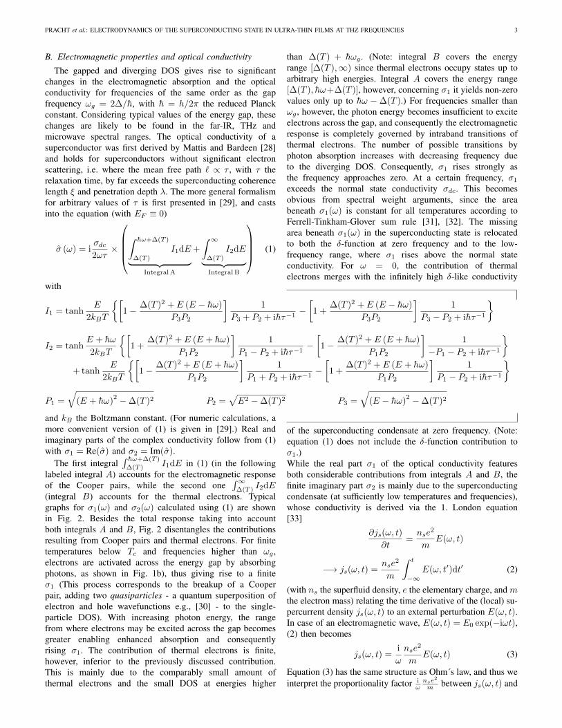
I2dE(integral B) accounts for the thermal electrons. Typicalgraphs for σ1(ω) and σ2(ω) calculated using (1) are shownin Fig. 2. Besides the total response taking into accountboth integrals A and B, Fig. 2 disentangles the contributionsresulting from Cooper pairs and thermal electrons. For finitetemperatures below Tc and frequencies higher than ωg ,electrons are activated across the energy gap by absorbingphotons, as shown in Fig. 1b), thus giving rise to a finiteσ1 (This process corresponds to the breakup of a Cooperpair, adding two quasiparticles - a quantum superposition ofelectron and hole wavefunctions e.g., [30] - to the single-particle DOS). With increasing photon energy, the rangefrom where electrons may be excited across the gap becomesgreater enabling enhanced absorption and consequentlyrising σ1. The contribution of thermal electrons is finite,however, inferior to the previously discussed contribution.This is mainly due to the comparably small amount ofthermal electrons and the small DOS at energies higher
than ∆(T ) + hωg . (Note: integral B covers the energyrange [∆(T ),∞) since thermal electrons occupy states up toarbitrary high energies. Integral A covers the energy range[∆(T ), hω+∆(T )], however, concerning σ1 it yields non-zerovalues only up to hω −∆(T ).) For frequencies smaller thanωg , however, the photon energy becomes insufficient to exciteelectrons across the gap, and consequently the electromagneticresponse is completely governed by intraband transitions ofthermal electrons. The number of possible transitions byphoton absorption increases with decreasing frequency dueto the diverging DOS. Consequently, σ1 rises strongly asthe frequency approaches zero. At a certain frequency, σ1
exceeds the normal state conductivity σdc. This becomesobvious from spectral weight arguments, since the areabeneath σ1(ω) is constant for all temperatures according toFerrell-Tinkham-Glover sum rule [31], [32]. The missingarea beneath σ1(ω) in the superconducting state is relocatedto both the δ-function at zero frequency and to the low-frequency range, where σ1 rises above the normal stateconductivity. For ω = 0, the contribution of thermalelectrons merges with the infinitely high δ-like conductivity
of the superconducting condensate at zero frequency. (Note:equation (1) does not include the δ-function contribution toσ1.)While the real part σ1 of the optical conductivity featuresboth considerable contributions from integrals A and B, thefinite imaginary part σ2 is mainly due to the superconductingcondensate (at sufficiently low temperatures and frequencies),whose conductivity is derived via the 1. London equation[33]
∂js(ω, t)
∂t=nse
2
mE(ω, t)
−→ js(ω, t) =nse
2
m
∫ t
−∞E(ω, t′)dt′ (2)
(with ns the superfluid density, e the elementary charge, and mthe electron mass) relating the time derivative of the (local) su-percurrent density js(ω, t) to an external perturbation E(ω, t).In case of an electromagnetic wave, E(ω, t) = E0 exp(−iωt),(2) then becomes
js(ω, t) =i
ω
nse2
mE(ω, t) (3)
Equation (3) has the same structure as Ohm´s law, and thus weinterpret the proportionality factor i
ωnse
2
m between js(ω, t) and
4 IEEE TRANSACTIONS ON THZ SCIENCE AND TECHNOLOGY, 2013
00
00
Re
(sc) =
1
T = 0.8TC 1/ = 40 x 2 (0)
dc
0 1 1
11
2 3
0
0
total response photon-activated thermally activated
Im (
sc) =
2
Frequency (2 (T)/h )10
0(a)
(b)
1/ 40 x 2 (0)
increasing 1/
increasing 1/
0.9TC
0.1TC
decreasing T
0.1TC
Frequency (2 (0)/h )
1
decreasing T 0.9TC
T = 0.8TC
Frequency (2 (0)/h )
T = 0.8TC
1/ 40 x 2 (0)
2
Frequency (2 (0) h ) Frequency (2 (0) h )
Fig. 2. (Color online)(a) Real and (b) imaginary parts of the complex opticalconductivity (solid line) of a superconductor as a function of frequency basedon (1) for T = 0.8Tc. Dashed lines disentangle the contributions of both thethermal electrons (Integral B in (1) and photon-activated electrons (Integral Ain (1) to the conductivity. Insets of (a) and (b) show σ1 and σ2 for differenttemperatures (T/Tc = 0.9, 0.8, 0.7, 0.6, 0.5, 0.4, 0.3, 0.2, and 0.1) andscattering rates (1/τ = 40, 20, 4, 2, 0.8, 0.4, and 0.04 ×2∆(0)), respectively.(Used parameters 2∆(0) = 25 cm−1, Tc = 10 K, σdc = 1066 Ω−1cm−1)
E(ω, t) as the conductivity of the superconducting condensate,which is purely imaginary and thus only contributes to σ2.Upon increasing frequency, σ2 decays as 1/ω. Consequently,the strongest contribution is at energies well below 2∆(T ),much lower than addressed in our study, i.e. at microwavefrequencies [34], [35]. Kramers-Kronig analysis underlines theabove qualitative picture yielding the same result [33]. IntegralA yields finite values up to hω + ∆(T ) which calls for theintegration range given in (1). For frequencies larger than ωg ,Cooper pairs are destroyed, and thus the overall out-of-phaseresponse changes. This is signaled by a weak kink of σ2 at theenergy gap, as shown in Fig. 2. In analogy to an electric LCcircuit, the frequency dependence of σ2 is often interpretedin terms of frequency dependent kinetic inductance [36], [37].The impedance of the circuit rises towards higher frequenciesleading to a reduced conductivity. A finite scattering rate 1/τaccounted for in (1) further influences the behavior of thecomplex conductivity. Upon increasing 1/τ (going from clean-limit to dirty-limit superconductors), the rise in σ1 for ω > ωgis gradually enhanced, and σ2 features a strongly pronouncedkink at ωg for scattering rates comparable to the energy gap,see insets of Fig. 2(a) and (b).
III. EXPERIMENT AND DATA PROCESSING
A. THz frequency-domain spectroscopy
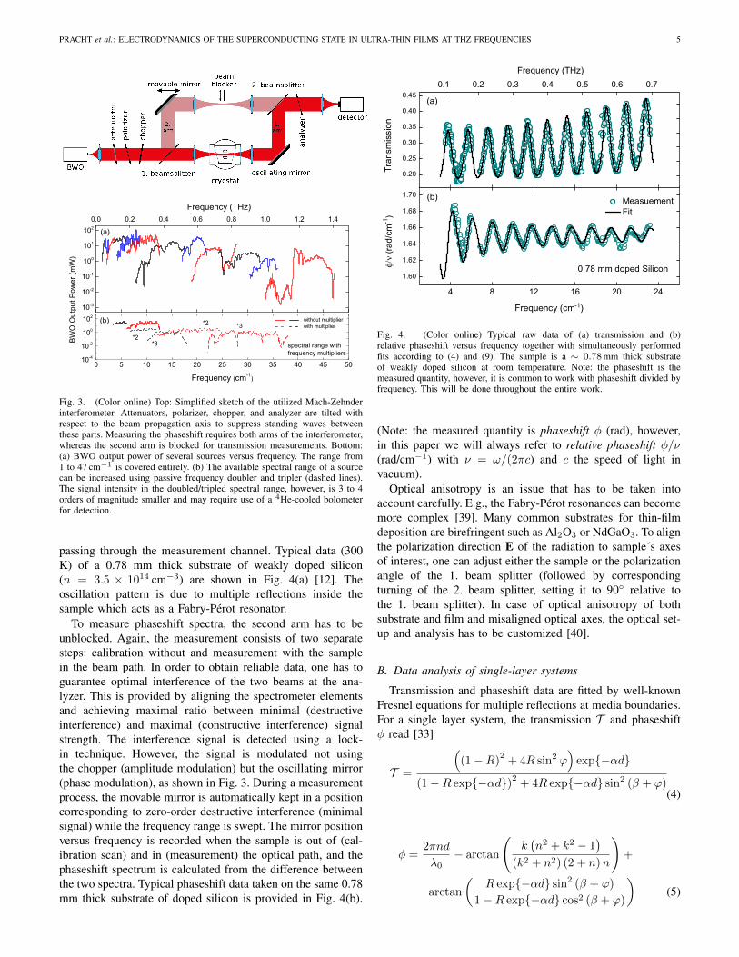
Our THz studies are based on the frequency-domain spec-troscopy technique. Coherent, monochromatic and continuousTHz radiation is generated by frequency-tunable backward-wave-oscillators (BWO) that provide frequencies from 1 to47 cm−1 [38]. This spectral range is covered by a numberof different BWO radiation sources (in the following justsources), see bottom of Fig. 3. The power of the radiationstrongly depends on the frequency and may be as large as100 mW for low-frequency and significantly smaller (0.1 mW)for high-frequency sources. As a consequence, the low-frequency radiation power might be too strong and requiresuse of attenuators to avoid sample heating or detector overload.The great benefit of FDS compared to time-domain spec-troscopy (TDS) is to process frequencies step by step witha stability and resolution exceeding ∆ω/ω = 10−6 dependingon the BWO power supply.
While TDS excites all available energies simultaneously andhas to struggle with minor signal strength, FDS can directlyprobe narrow-band excitations and resolve detailed line shapes.The high output power leads to high signal-to-noise ratio thatcan reach values up to 106. Frequency doublers and triplers(Virginia Diodes) that allow extending the frequency range of aseparate source can effectively be used. Loss of the radiationintensity is easily compensated by use of a 4He bolometer(see below). After the radiation is generated by the BWO, it iscollimated by a Teflon, quartz, or polyethylene lens and guidedby aluminum mirrors and wire grids, see top of Fig. 3, whichact as beam splitters depending on polarization. Other lensesare used to focus the radiation on the sample under study andthe detector. Attenuators, polarizer, chopper, and analyzer aretilted with respect to the beam propagation axis to suppressstanding waves between these parts. The quasi-optical part ofthe experiment is a Mach-Zehnder interferometer which allowsus to measure both amplitude and phaseshift of THz radiationpassing through a sample. The radiation is detected by either aGolay cell or a 4He-cooled bolometer (Infrared Laboratories),depending on signal strength. For transmission measurements,the radiation is mechanically chopped to make it detectableusing a lock-in technique.
Determining the spectra of optical parameters of the plane-parallel sample involves measurements of the transmissionand phaseshift spectra from which the spectra of real andimaginary parts of complex permittivity, conductivity, etc., arecalculated directly and without use of any additional analysis(such as Kramers-Kronig analysis).
Recording a transmission spectrum is performed with thesecond arm of the interferometer blocked. It consists of twoseparate steps. First, the signal intensity versus frequency isrecorded with no sample in the beam path. This transmis-sion spectrum is regarded 100% transmission and used asmeasurement calibration. Second, the transmission spectrumis recorded with the sample in the beam path and the absolutetransmission spectrum is obtained as a result of division of thetwo corresponding data arrays. In this way we can accountfor the frequency-dependent output power of the radiation
PRACHT et al.: ELECTRODYNAMICS OF THE SUPERCONDUCTING STATE IN ULTRA-THIN FILMS AT THZ FREQUENCIES 5
10-3
10-2
10-1
100
101
102
(b)
BWO
Out
put P
ower
(mW
)
(a)
0 5 10 15 20 25 30 35 40 45 5010-4
10-2
100
102
*2 *3
*3
without multiplier with multiplier
Frequency (cm-1)
spectral range withfrequency multipliers
*2
0.0 0.2 0.4 0.6 0.8 1.0 1.2 1.4
Frequency (THz)
Fig. 3. (Color online) Top: Simplified sketch of the utilized Mach-Zehnderinterferometer. Attenuators, polarizer, chopper, and analyzer are tilted withrespect to the beam propagation axis to suppress standing waves betweenthese parts. Measuring the phaseshift requires both arms of the interferometer,whereas the second arm is blocked for transmission measurements. Bottom:(a) BWO output power of several sources versus frequency. The range from1 to 47 cm−1 is covered entirely. (b) The available spectral range of a sourcecan be increased using passive frequency doubler and tripler (dashed lines).The signal intensity in the doubled/tripled spectral range, however, is 3 to 4orders of magnitude smaller and may require use of a 4He-cooled bolometerfor detection.
passing through the measurement channel. Typical data (300K) of a 0.78 mm thick substrate of weakly doped silicon(n = 3.5 × 1014 cm−3) are shown in Fig. 4(a) [12]. Theoscillation pattern is due to multiple reflections inside thesample which acts as a Fabry-Perot resonator.
To measure phaseshift spectra, the second arm has to beunblocked. Again, the measurement consists of two separatesteps: calibration without and measurement with the samplein the beam path. In order to obtain reliable data, one has toguarantee optimal interference of the two beams at the ana-lyzer. This is provided by aligning the spectrometer elementsand achieving maximal ratio between minimal (destructiveinterference) and maximal (constructive interference) signalstrength. The interference signal is detected using a lock-in technique. However, the signal is modulated not usingthe chopper (amplitude modulation) but the oscillating mirror(phase modulation), as shown in Fig. 3. During a measurementprocess, the movable mirror is automatically kept in a positioncorresponding to zero-order destructive interference (minimalsignal) while the frequency range is swept. The mirror positionversus frequency is recorded when the sample is out of (cal-ibration scan) and in (measurement) the optical path, and thephaseshift spectrum is calculated from the difference betweenthe two spectra. Typical phaseshift data taken on the same 0.78mm thick substrate of doped silicon is provided in Fig. 4(b).
0.20
0.25
0.30
0.35
0.40
0.45
Measuement Fit
Tran
smis
sion
(a)
4 8 12 16 20 24
1.60
1.62
1.64
1.66
1.68
1.70
(ra
d/cm
-1)
Frequency (cm-1)
(b)
0.78 mm doped Silicon
0.1 0.2 0.3 0.4 0.5 0.6 0.7 Frequency (THz)
Fig. 4. (Color online) Typical raw data of (a) transmission and (b)relative phaseshift versus frequency together with simultaneously performedfits according to (4) and (9). The sample is a ∼ 0.78 mm thick substrateof weakly doped silicon at room temperature. Note: the phaseshift is themeasured quantity, however, it is common to work with phaseshift divided byfrequency. This will be done throughout the entire work.
(Note: the measured quantity is phaseshift φ (rad), however,in this paper we will always refer to relative phaseshift φ/ν(rad/cm−1) with ν = ω/(2πc) and c the speed of light invacuum).
Optical anisotropy is an issue that has to be taken intoaccount carefully. E.g., the Fabry-Perot resonances can becomemore complex [39]. Many common substrates for thin-filmdeposition are birefringent such as Al2O3 or NdGaO3. To alignthe polarization direction E of the radiation to sample´s axesof interest, one can adjust either the sample or the polarizationangle of the 1. beam splitter (followed by correspondingturning of the 2. beam splitter, setting it to 90 relative tothe 1. beam splitter). In case of optical anisotropy of bothsubstrate and film and misaligned optical axes, the optical set-up and analysis has to be customized [40].
B. Data analysis of single-layer systems
Transmission and phaseshift data are fitted by well-knownFresnel equations for multiple reflections at media boundaries.For a single layer system, the transmission T and phaseshiftφ read [33]
T =
((1−R)
2+ 4R sin2 ϕ
)exp−αd
(1−R exp−αd)2+ 4R exp−αd sin2 (β + ϕ)
(4)
φ =2πnd
λ0− arctan
(k(n2 + k2 − 1
)(k2 + n2) (2 + n)n
)+
arctan
(R exp−αd sin2 (β + ϕ)
1−R exp−αd cos2 (β + ϕ)
)(5)

6 IEEE TRANSACTIONS ON THZ SCIENCE AND TECHNOLOGY, 2013
where R = (1 − 2n + n2 + k2)(1 + 2n + n2 + k2)−1 is thereflectivity, ϕ = arctan−2k(1 − n2 − k2)−1 is the phasechange upon reflection at an interface between the two media,β = 2πnd/λ0 is the angle by which the phase of the radiationis changed upon travelling through a medium of thickness dfor a given wavelength λ0 and α = 4πk/λ0 is the powerabsorption coefficient. The quantities n, k are real and imagi-nary parts of the complex refractive index
√ε = n = n + ik
in the given case of a non-magnetic material. Equations (4)and (5) do not account for any frequency dependence forthe optical constants n and k, which typically depend onfrequency and reveal the properties of interest in this study.To include resonant absorption (e.g. Lorentz oscillators) orconductivity (Drude behavior), corresponding terms are used.For example, to describe the free carrier response withinthe Drude conductivity model we can introduce complexpermittivity ε = ε1 + iε2, and e.g., in case of a simple metalthe Drude formula [33]
ε1(ω) = ε∞ −ω2p
ω2 + τ−2(6)
ε2(ω) =1
ωτ
ω2p
ω2 + τ−2(7)
or rewritten in terms of the complex optical conductivityσ(ω) = i ω4π (ε∞ − ε(ω))
σ1(ω) = σdc1
1 + ω2τ2(8)
σ2(ω) = σdcωτ
1 + ω2τ2(9)
where ωp is the plasma frequency, σdc = ω2P τ/4π is the dc
conductivity, ε∞ is the value of the dielectric constant forfrequencies much higher than addressed in this study, and 1/τis the relaxation rate. The solid lines in Fig. 4 are fits basedupon (4) and (5). The fitting parameters n and k are expressedin terms of ε1, ε2, σ1 and σ2 using well-known expressions,[33], and, by this, the frequency dependence according toDrude theory enters the transmission and phaseshift fits via(6)-(9). Clearly, this yields an excellent description of theexperimental data, i.e. this silicon substrate is a text bookrepresentative of optical Drude behavior [41]–[43].
Another analysis approach is to fit the Fabry-Perot trans-mission peaks separately, with two advantages: first, the noiseis least pronounced in the vicinity of the Fabry-Perot max-ima, and the largest sensitivity is reached here. Second, thisroutine provides more freedom in the case of materials withunknown properties where no explicit function for frequencydependence is known. To do so, each Fabry-Perot maximumat some given frequency ω0 is fitted separately and yields aset of material parameters at ω0. Processing each Fabry-Perottransmission peak in this way eventually yields the desiredfrequency-dependent optical functions.
C. Data analysis of multi-layer systems
Equations (4) and (5) hold for a single layer. For a two(or more)- layer system, however, another boundary has to be
0.0
0.2
0.4
0.6
0.8
12 K4.2 K
4.2 K
(b)
Tran
smis
sion
(a)
12 K
3 4 5 6 7 8 9 100.0
0.2
0.4
0.6
side view
cryo 1 cryo 2
(rad
/cm
-1)
Frequency (cm-1)
Cryostat 1 (parallel windows) Cryostat 2 (tilted windows)NbN, Tc = 11.8 K
top view
0.12 0.16 0.20 0.24 0.28
Frequency (THz)
standing waves
Fig. 5. (Color online) Raw transmission (a) and relative phaseshift (b) versusfrequency measured with parallel-outer-window cryostat ”1” (filled circles)and tilted-outer-window cryostat ”2” (open circles) at two temperatures 4.2and 12 K (sample: NbN, Tc = 11.8 K). Towards low frequencies, standingwaves are strongly pronounced for cryostat ”1”. With increasing frequency thestanding waves become less pronounced. Simplified sketches of the windowarrangement in top- and side-view positions of both cryostats are shown in(b).
accounted for. To disentangle properties of the two media (e.g.film on a substrate) the two experimental quantities (trans-mission and phaseshift) have to be measured. The responsefunctions of the film are calculated from the two correspondingspectra. This requires detailed knowledge of the substrateparameters, which have to be determined beforehand in aseparate experiment. The Fresnel equations are extended byterms describing another boundary reflection and are foundelsewhere e.g., [33] or [44]. To improve the interaction ofprobing radiation with the material under study, a resonantFabry-Perot technique has been developed where two speci-mens of the thin film under study are mounted face-to-facerealizing a resonant cavity [45]. This technique is useful incase of superconducting films, where it can be difficult toobtain the dynamical conductivity σ1 with sufficient accuracydue to huge positive values of σ2. Fabrication of such aresonant cavity, however, remains a challenging task [45].
D. Optical cryostats for THz spectroscopy and standing-waveproblem
To access low temperatures we employ two different home-built 4He-bath cryostats labeled ”1” and ”2” here. The mostnotable difference among these cryostats is the arrangementof the optical inner and outer windows. Diffraction and stand-ing waves distorting the measured spectra become a severeproblem especially at low frequencies below 10 cm−1, sincethe THz radiation wavelength becomes of the same order astypical setup dimensions, e.g. the distances between innerwindows of the cryostat, polarizers, lenses, etc.. To reducethis problem, the windows are made of thin Mylar (∼ 20µm)foils which are slightly curved due to inner vacuum. The outerwindows of cryostat ”1” are oriented perpendicularly to the
PRACHT et al.: ELECTRODYNAMICS OF THE SUPERCONDUCTING STATE IN ULTRA-THIN FILMS AT THZ FREQUENCIES 7
8.5 9.0 9.5 10.0 10.5 11.0 11.50
150
300
450
600
(b)
TaN on sapphire
80 mA - 4.9 nm 100 mA - 5.1 nm 110 mA - 4.9 nm 120 mA - 4.9 nm 70 mA - 5.0 nm
She
et R
esis
tanc
e (
)
Temperature (K)
(a)
8 10 12 14 16 180
150
300
450
600
175 mA - 3.9 nm 100 mA - 4.1 nm 145 mA - 4.2 nm 190 mA - 4.4 nm 200 mA - 4.7 nm
NbN on sapphire
Shee
t Res
ista
nce
()
Temperature (K)
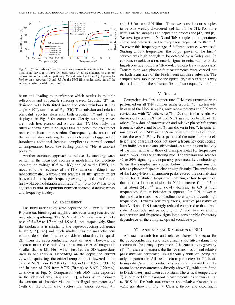
Fig. 6. (Color online) Sheet dc resistance versus temperature for differentfilms of (a) TaN and (b) NbN. Different values of Tc are obtained for differentdeposition currents while sputtering. We estimate the Ioffe-Regel parameterkF ` to vary between 4.5 and 5.5 for the NbN films under study far off thesuperconductor-insulator transition.
beam still leading to interference which results in multiplereflections and noticeable standing waves. Cryostat ”2” wasdesigned with both tilted inner and outer windows (tiltingangle ∼10), see inset of Fig. 5(b). Transmission and relativephaseshift spectra taken with both cryostat ”1” and ”2” aredisplayed in Fig. 5 for comparison. Clearly, standing wavesare much less pronounced on cryostat ”2”. Obviously, thetilted windows have to be larger than the non-tilted ones to notreduce the beam cross section. Consequently, the amount ofthermal radiation entering the sample chamber is bigger whichintroduces additional heating, complicating thermal controlat temperatures below the boiling point of 4He at ambientpressure.
Another common approach to reduce the standing wavepattern in the measured spectra is modulating the electron-acceleration voltage (0.5 to 6 kV) applied to the BWO, i.e.modulating the frequency of the THz radiation making it lessmonochromatic. Narrow-band features of the spectra mightbe washed out by this frequency averaging, and therefore thehigh-voltage-modulation amplitude Vp−p (0 to 50 V) has to beadjusted to find an optimum between reduced standing wavesand frequency fidelity.
IV. EXPERIMENT
The films under study were deposited on 10 mm × 10 mmR-plane-cut birefringent sapphire substrates using reactive dc-magnetron sputtering. The NbN and TaN films have a thick-ness of d= 3.9 to 4.7 nm and 4.9 to 5.1 nm, respectively. Sincethe thickness d is similar to the superconducting coherencelength ξ [5], [46] and much smaller than the magnetic pen-etration depth, the films are considered ultra-thin, i.e. quasi-2D, from the superconducting point of view. However, theelectron mean free path ` is about one order of magnitudesmaller than d [5], [46], which justifies the 3D expressionsused in our analysis. Depending on the deposition currentId while sputtering, the critical temperature is lowered in thecase of NbN from 12.2 K (Id = 100 mA) to 8.5 K (200 mA)and in case of TaN from 9.7 K (70 mA) to 8.6 K (120 mA),as shown in Fig. 6. Comparison with NbN film depositedin the identical way [46] and [11], allows us to estimatethe amount of disorder via the Ioffe-Regel parameter kF `(with kF the Fermi wave vector) that varies between 4.5
and 5.5 for our NbN films. Thus, we consider our samplesto be only weakly disordered and far off the SIT. For moredetails on the samples and deposition process see [47] and [6].We investigate several NbN and TaN samples at temperaturesabove and below Tc in the frequency range 3.4 to 38 cm−1.To cover this frequency range, 5 different sources were used.Starting at low frequencies, the output power of the first 4sources was high enough to be detected by a Golay cell. Incontrast, to achieve a reasonable signal-to-noise ratio with thehigh-frequency source, a 4He-cooled bolometer was necessary.Transmission and phaseshift measurements were carried outon both main axes of the birefringent sapphire substrate. Thesamples were mounted into the optical cryostats in such a waythat radiation hits the substrate first and subsequently the film.
V. RESULTS
Comprehensive low temperature THz measurements wereperformed on all TaN samples using cryostat ”2” exclusively.In case of the NbN samples, only measurements at 4.2 K werecarried out with ”2” otherwise ”1”. Due to similar results wediscuss only one TaN and one NbN sample on behalf of theothers. Raw data of transmission and relative phaseshift versusfrequency above and below Tc are shown in Fig. 7. In general,raw data of both NbN and TaN are very similar. In the normalstate, the overall Fabry-Perot pattern of the transmission coef-ficient and phaseshift does not show a frequency dependence.This indicates a constant dispersionless complex conductivityof the film, similar to those of a simple metal for frequenciesmuch lower than the scattering rate. The transmission reaches45 to 50% signaling a comparably poor metallic conductivity.When the samples are cooled below Tc, transmission andrelative phaseshift spectra change significantly. The amplitudesof the Fabry-Perot transmission peaks exceed the normal-statevalues for all studied frequencies. Starting at low frequencies,the maxima in transmission in NbN increase from 0.7 to1 at about 24 cm−1 and slowly decrease to 0.9 at highfrequencies. Similar behavior is apparent for TaN, however,the maxima in transmission decline more rapidly towards highfrequencies. Towards low frequencies, relative phaseshift ofboth NbN and TaN is strongly reduced compared to the normalstate. Amplitude and periodicity of T and φ/ω vary withtemperature and frequency signaling a considerable frequencydependence of the complex optical conductivity.
VI. ANALYSIS AND DISCUSSION OF NbN
All raw transmission and relative phaseshift spectra forthe superconducting state measurments are fitted taking intoaccount the frequency dependence of the conductivity given by(1). For each temperature, the fits for transmission and relativephaseshift are performed simultaneously with 2∆ being theonly fit parameter. All free-electron parameters in (1) (scat-tering rate 1/τ and dc conductivity σdc) are obtained from thenormal-state measurements directly above Tc, which are fittedto Drude theory and taken as constant. The critical temperatureTc is obtained from transport measurements, as shown in Fig.6. BCS fits for both transmission and relative phaseshift at4.2 K are shown in Fig. 7. Clearly, theory and experiment
8 IEEE TRANSACTIONS ON THZ SCIENCE AND TECHNOLOGY, 2013
0.0
0.2
0.4
0.6
0.8
1.0
Tran
smis
sion
0.4
0.5
0.6
0.7
(c)
(b)
(d)
(a)
TaN filmTc = 9.7 K
TaN filmTc = 9.7 K
NbN filmTc = 9.7 K
(rad
/cm
-1)
4.2 K 11 K BCS fit Drude fit
NbN filmTc = 9.7 K
0.0
0.2
0.4
0.6
0.8
1.0
Tran
smis
sion
10 20 30 40
0.4
0.5
0.6
0.7
(rad
/cm
-1)
Frequency (cm-1)
4. 2 K 20 K BCS fit Drude fit
Frequency (THz)0.2 0.4 0.6 0.8 1.0
Fig. 7. (Color online) Raw transmission of (a) NbN and (c) TaN and relativephaseshift of (b) NbN and (d) TaN versus frequency at two temperatures, 4.2 Kand in the normal state. Solid lines are transmission and relative phaseshift fitswith the optical conductivity given by (6) and (7) in the normal state, and (1)at 4.2 K. The vertical dashed lines mark the gap frequency νg = ωg/(2πc) ≈28 cm−1 (NbN) and νg = ωg/(2πc) ≈ 21.7 cm−1 (TaN).
match very well for frequencies both above and below theenergy gap. The same holds for the other temperatures, whichallows to extract 2∆ for each temperature precisely. Fig. 8displays the temperature dependent energy gap 2∆(T ) of thesample with lowest disorder and highest Tc. Filled and opensymbols refer to different main axes of the substrate andcoincide within the range of error δ2∆ = 0.9 meV. Data foreach main axis is fitted separately with the BCS expression[48]
∆(T )
∆(0)= tanh
TcT
∆(T )
∆(0)
. (10)
For 0.3Tc < T < 0.8Tc the measured energy gap is slightlyabove the BCS curve and for 0.8Tc < T < Tc below. Thelow-temperature part displays a similar behavior as it hasbeen observed in microwave experiments [49], where 2∆(T )does not decrease as fast as in BCS theory as T → Tc.
0 2 4 6 8 10 120
1
2
3
4
(c)(b)
2 (m
eV)
+ axis - axis BCS (+ axis) BCS (- axis)
Temperature (K)
NbN Tc = 12.2 K
(a)
0
5
10
15
20
25
30
2 (c
m-1)
8 9 10 11 12
Critical Temperature Tc (K)
weak-coupling BCS 3.6
3.9
4.2
4.5
2(0
)/kBT
c
8 9 10 11 12
3.2
3.6
4.0
4.4
mea
n en
ergy
gap
(4
.2 K
) (m
eV)
Critical Temperature Tc (K)
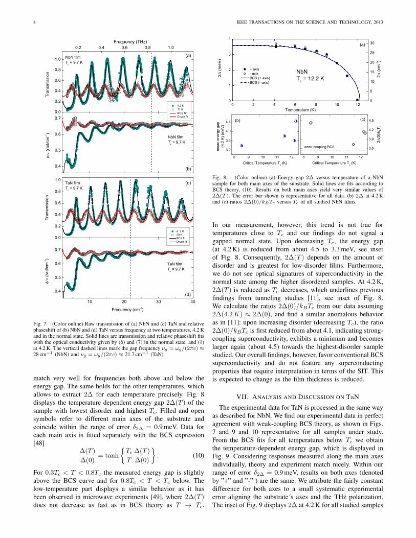
Fig. 8. (Color online) (a) Energy gap 2∆ versus temperature of a NbNsample for both main axes of the substrate. Solid lines are fits according toBCS theory, (10). Results on both main axes yield very similar values of2∆(T ). The error bar shown is representative for all data. (b) 2∆ at 4.2 Kand (c) ratios 2∆(0)/kBTc versus Tc of all studied NbN films.
In our measurement, however, this trend is not true fortemperatures close to Tc and our findings do not signal agapped normal state. Upon decreasing Tc, the energy gap(at 4.2 K) is reduced from about 4.5 to 3.3 meV, see insetof Fig. 8. Consequently, 2∆(T ) depends on the amount ofdisorder and is greatest for low-disorder films. Furthermore,we do not see optical signatures of superconductivity in thenormal state among the higher disordered samples. At 4.2 K,2∆(T ) is reduced as Tc decreases, which underlines previousfindings from tunneling studies [11], see inset of Fig. 8.We calculate the ratios 2∆(0)/kBTc from our data assuming2∆(4.2K) ≈ 2∆(0), and find a similar anomalous behavioras in [11]: upon increasing disorder (decreasing Tc), the ratio2∆(0)/kBTc is first reduced from about 4.1, indicating strong-coupling superconductivity, exhibits a minimum and becomeslarger again (about 4.5) towards the highest-disorder samplestudied. Our overall findings, however, favor conventional BCSsuperconductivity and do not feature any superconductingproperties that require interpretation in terms of the SIT. Thisis expected to change as the film thickness is reduced.
VII. ANALYSIS AND DISCUSSION ON TaN
The experimental data for TaN is processed in the same wayas described for NbN. We find our experimental data in perfectagreement with weak-coupling BCS theory, as shown in Figs.7 and 9 and 10 representative for all samples under study.From the BCS fits for all temperatures below Tc we obtainthe temperature-dependent energy gap, which is displayed inFig. 9. Considering responses measured along the main axesindividually, theory and experiment match nicely. Within ourrange of error δ2∆ = 0.9 meV, results on both axes (denotedby ”+” and ”-” ) are the same. We attribute the fairly constantdifference for both axes to a small systematic experimentalerror aligning the substrate´s axes and the THz polarization.The inset of Fig. 9 displays 2∆ at 4.2 K for all studied samples

PRACHT et al.: ELECTRODYNAMICS OF THE SUPERCONDUCTING STATE IN ULTRA-THIN FILMS AT THZ FREQUENCIES 9
0 1 2 3 4 5 6 7 8 9 100.0
0.5
1.0
1.5
2.0
2.5
3.0
3.5
(c)(b)
2 (m
eV)
Temperature (K)
+ axis - axis BCS (+ axis) BCS (- axis)
TaN Tc = 9.7 K
(a)
0
5
10
15
20
25
2 (c
m-1)
8.5 9.0 9.5 10.0
2.4
2.6
2.8
3.0
mea
n en
ergy
gap
(4.2
K) (
meV
)
Critical Temperature Tc (K)
8.5 9.0 9.5 10.0
Critical Temperature Tc (K)
weak-coupling BCS
3.2
3.6
4.0
2/k
BT c
Fig. 9. (Color online)(a) Energy gap 2∆ versus temperature for both mainaxes of the substrate (denoted by ”+” and ”-” ). Solid lines are fits accordingto BCS theory, (10). Considering each axis separately, experiment and theorymatch nicely. The error bar shown is representative for all data. (b) 2∆ at4.2 K and (c) ratios 2∆(0)/kBTc versus Tc of all studied TaN films
versus Tc. While 2∆ tends to decrease as Tc is reduced inthe case of NbN, we do not see a significant dependencefor TaN. Since the ratio between highest and lowest criticaltemperatures Tmaxc /Tminc is 1.13 and 1.44 for TaN and NbN,respectively, we can only access a smaller range here whichmakes it difficult to establish similar conclusions from ourTaN experiments. We calculate the ratio 2∆(0)/kBTc fromour experimental data to be closely scattered around the weak-coupling prediction 3.52 [23], which underlines pure weak-coupling BCS superconductivity in this range of disorder andcritical temperatures.
We also analyze the raw data with single-peak fits toextract the frequency dependence of the complex conductivityσ(ω) = σ1(ω) + iσ2(ω) independently from a predefinedmodel. For this, a narrow frequency range of 0.5 to 1 cm−1 ischosen for fitting each single Fabry-Perot peak separately withε1 and ε2 as fitting parameters. Subsequently, σ1 and σ2 arecalculated via ε = ε∞+i4πσ/ω for each peak frequency withε∞ = 1. Fig. 10 displays the conductivity for 4.2 and 7 K wellbelow Tc = 9.7 K and at 20 K in the normal state. Closedand open symbols are for the different main axes. Data pointscorresponding to different main axes are shifted in frequency.The reason is that ε1 of the birefringent substrate is slightlydifferent for both axes leading to a shift in peak position. Thesolid lines are BCS predictions based on the raw-data fits.Within the range of error, theory and experiment (for bothmain axes) match reasonably. 2∆(T ) is signaled by the kink inσ1 and is clearly resolved within the experimental frequencyrange. At 20 K, σ1 does not depend on the frequency andcorresponds to the constant value σ1 = σdc = 4580 Ω−1cm−1
extracted from Drude fits. The studied frequency range is wellbelow the scattering rate 1/τ and, thus, σ2 is immeasurablysmall in the normal state at 20 K. In the superconducting state,however, σ2 rises notably and approaches the zero-temperatureprediction σ2(T = 0) ∝ ω−1 for hω < 2∆(T ) , which
is consistent with the δ-function-like conductivity σ1 at zerofrequency. This trend in σ2 is also seen in the superconductingpenetration depth λL. The inset of Fig. 10(b) displays λLversus frequency for both main axes at 4.2 and 7 K calculatedvia [33]
λL =
√c2
4πωσ2. (11)
For frequencies hω < 2∆(T ) and a δ-function-like σ1,λL does not significantly depend on frequency. Despite thefinite temperatures, such frequency-independent behavior issupported by the data in Fig. 10. At 4.2 K, λL remains fairlyconstant for frequencies lower than 24 cm−1 and approaches∼ 500 nm for ω → 0. At 7 K, similar behavior is apparent forfrequencies lower than 15 cm−1, and λL approaches ∼ 600nm. The zero-frequency values of λL are very similar to onesobtained from previous transport measurements [50]. By andlarge, we find the charge carrier dynamics of our TaN filmsto be perfectly described within weak-coupling BCS theory.
0
1x10³
2x10³
3x10³
4x10³
5x10³
20 K
7 K
1 (-1cm
-1)
+ axis - axis
BCS (+ axis) BCS (- axis)
4.2 K
(a)
0.0 0.2 0.4 0.6 0.8 1.0
Frequency (THz)
0 10 20 30 400.0
5.0x10³
1.0x10⁴
1.5x10⁴
2.0x10⁴
2.5x10⁴
7 K
2 (-1cm
-1)
Frequency (cm-1)
4.2 K
TaN Tc=9.7 K
(b)
5 10 15 20 25 300
1
2
3
4 4.2 K 7 K
L(m
)
Frequency (cm-1)
Fig. 10. (Color online) Real part (a) and imaginary part (b) of the complexconductivity versus frequency for 4.2 and 7 K well below Tc and 20 K inthe normal state for both main axes of a TaN sample. Solid and dashedlines are predictions calculated directly from raw data fits for both axesindividually. The shift in frequency is caused by different peak positionsdue to birefringence. The kink in σ1 signaling the energy gap is resolvedclearly. The error bar shown is representative for all data. The inset shows thepenetration depth as a function of frequency. λL is frequency independent forhω < 2∆(T ).
VIII. SUMMARY
We have described the performance and characteristics ofour frequency-domain THz spectroscopic experimental tech-niques. Furthermore, we give a comprehensive overview ofthe analyses we employ and the theoretical foundation onwhich they are based. We studied charge carrier dynamicsand superconducting properties of NbN and TaN thin filmswith different values of Tc at low temperatures above andbelow Tc in the THz frequency range from 0.09 to 1.1 THz
10 IEEE TRANSACTIONS ON THZ SCIENCE AND TECHNOLOGY, 2013
(3 to 38 cm−1). Coherent and continuous THz radiation wasgenerated by frequency-tunable high power backward waveoscillators covering the frequency range below and abovethe energy gap 2∆(T ). We fit our experimental data oftransmission and phaseshift to a combination of Fresnel equa-tions, BCS- and Drude theory and describe superconductingproperties and charge carrier dynamics. The results for bothNbN and TaN are very well described within the framework ofBCS theory. The agreement between our results and previousmeasurements on NbN from another group confirm that ourexperimental approach is perfectly suited to study correlatedelectron phenomena in thin film systems. The dependence ofthe ratio 2∆(0)/kBTc and 2∆ on Tc we obtain for our NbNfilms resemble anomalous behavior as it has been reportedpreviously, whereas the ratios for our TaN films do notsignificantly deviate from the weak-coupling BCS prediction.Absolute values of 2∆ and the ratio 2∆(0)/kBTc for NbNare in good agreement with previous publications, and thusunderline the reliability and accuracy of our experiment andanalyses. This also endorses our results on TaN, a compoundthat so far has not been studied in detail concerning THzcharge carrier dynamics.
IX. ACKNOWLEDGMENT
We would like to thank Sina Zapf for fruitful discussion,Qiao Guo for help preparing the TaN samples, Elena Zhukovafor critically reading the manuscript, and the DFG for financialsupport. This study was partly financially supported by theRussian Foundation for Basic Research (project11-02-00199-a).
REFERENCES
[1] D. Sherman, G. Kopnov, D. Shahar, and A. Frydman, “Measurementof a superconducting energy gap in a homogeneously amorphousinsulator,” Phys. Rev. Lett., vol. 108, p. 177006, Apr 2012. [Online].Available: http://link.aps.org/doi/10.1103/PhysRevLett.108.177006
[2] B. Sacepe, B., C. Chapelier, T. I. Baturina, V. M. Vinokur, M. R.Baklanov, and M. Sanquer, “Pseudogap in an thin film of a conventionalsuperconductor,” Nature Communications, vol. 1, p. 140, 2010.
[3] Y. Mizukami, H. Shishido, T. Shibauchi, M. Shimozawa, S. Yasumoto,D. Watanabe, M. Yamashita, H. Ikeda, T. Terashima, H. Kontani, andY. Matstuda, “Extremely strong-coupling superconductivity in artificialtwo-dimensional Kondo lattices,” Nature Physics, vol. 7, p. 849853,2011. [Online]. Available: http://www.nature.com/nphys/journal/v7/n11/full/nphys2112.html
[4] M. R. Vissers, M. P. Weides, J. S. Kline, M. Sandberg, and D. P.Pappas, “Identifying capacitive and inductive loss in lumped elementsuperconducting hybrid titanium nitride/aluminum resonators,” AppliedPhysics Letters, vol. 101, p. 022601, 2012.
[5] A. Engel, A. Schilling, K. Il’in, and M. Siegel, “Dependence of countrate on magnetic field in superconducting thin-film TaN single-photondetectors,” Phys. Rev. B, vol. 86, p. 140506, Oct 2012. [Online].Available: http://link.aps.org/doi/10.1103/PhysRevB.86.140506
[6] D. Henrich, S. Dorner, M. Hofherr, K. Il’in, A. Semenov, E. Heintze,M. Scheffler, M. Dressel, and M. Siegel, “Broadening of hot-spot response spectrum of superconducting NbN nanowire single-photon detector with reduced nitrogen content,” Journal of AppliedPhysics, vol. 112, no. 7, p. 074511, 2012. [Online]. Available:http://link.aip.org/link/?JAP/112/074511/1
[7] A. J. Kerman, E. A. Dauler, W. E. Keichler, K. K. Yang, J. K.W. Bergren, G. Goltsman, and B. Voronov, “Kinetic-inductance-limitedreset time of superconducting nanowire photon counters,” Appl. Phys.Lett., vol. 88, p. 111116, 2006.
[8] G. Goltsman, O. Okunev, G. Chulkove, A. Lipatov, K. Dzadanov,A. Smirnov, A. Semenov, B. Voronov, C. Williams, and R. Sobolewski,“Fabrication and properties of an ulrafast NbN hot-electron single photondetector,” IEEE Trans. Appl. Supercond., vol. 11, pp. 574–577, 2001.
[9] J. Zhang, W. Slysz, A. Verevkin, O. Okunev, G. Chulkova, A. Korneev,A. Lipatov, G. Goltsman, and R. Sobolewski, “Response time character-ization on NbN superconducting single photon detectors,” IEEE Trans.Appl. Supercond., vol. 13, pp. 180–183, 2003.
[10] C. M. Natarajan, M. G. Tanner, and R. H. Hadfields, “Superconductingnanowire single-photon detectors: physics and applications,” Supercon-ductor Science and Technology, vol. 25, p. 063001, 2012.
[11] S. P. Chockalingam, M. Chand, A. Kamlapure, J. Jesudasan,A. Mishra, V. Tripathi, and P. Raychaudhuri, “Tunneling studies ina homogeneously disordered s-wave superconductor: NbN,” Phys.Rev. B, vol. 79, p. 094509, Mar 2009. [Online]. Available:http://link.aps.org/doi/10.1103/PhysRevB.79.094509
[12] U. S. Pracht, M. Scheffler, M. Dressel, D. F. Kalok, C. Strunk,and T. I. Baturina, “Direct observation of the superconducting gapin a thin film of titanium nitride using terahertz spectroscopy,”Phys. Rev. B, vol. 86, p. 184503, Nov 2012. [Online]. Available:http://link.aps.org/doi/10.1103/PhysRevB.86.184503
[13] E. F. C. Driessen, P. C. J. J. Coumou, R. R. Tromp, P. J.de Visser, and T. M. Klapwijk, “Strongly disordered tin and nbtins-wave superconductors probed by microwave electrodynamics,” Phys.Rev. Lett., vol. 109, p. 107003, Sep 2012. [Online]. Available:http://link.aps.org/doi/10.1103/PhysRevLett.109.107003
[14] M. Beck, M. Klammer, S. Lang, P. Leiderer, V. V. Kabanov, G. N.Gol’tsman, and J. Demsar, “Energy-gap dynamics of superconductingNbN thin films studied by time-resolved terahertz spectroscopy,”Phys. Rev. Lett., vol. 107, p. 177007, Oct 2011. [Online]. Available:http://link.aps.org/doi/10.1103/PhysRevLett.107.177007
[15] B. Gorshunov, I. V. Federov, G. V. Kozlov, A. Volkov, and A. Semenov,“Dynamic conductivity and the coherence peak in the submillimeterspectra of superconducting NbN films,” Solid State Communications,vol. 87, pp. 17–21, 1993.
[16] R. Matsunaga and R. Shimano, “Nonequilibrium bcs state dynamicsinduced by intense terahertz pulses in a superconducting nbn film,”Phys. Rev. Lett., vol. 109, p. 187002, Oct 2012. [Online]. Available:http://link.aps.org/doi/10.1103/PhysRevLett.109.187002
[17] R. Tesar, J. Kolacek, Z. Simsa, M. Sindler, L. Skrbek, K. Il’in, andM. Siegel, “Terahertz transmission of NbN superconductor thin film,”Physica C, vol. 19, pp. 932–934, 2010.
[18] R. Tesar, M. Sindler, K. Il’in, J. Kolacek, M. Siegel, andL. Skrbek, “Terahertz thermal spectroscopy of a NbN superconductor,”Phys. Rev. B, vol. 84, p. 132506, Oct 2011. [Online]. Available:http://link.aps.org/doi/10.1103/PhysRevB.84.132506
[19] M. Sindler, R. Tesar, J. Kolacek, L. Skrbek, and Z. Simsa,“Far-infrared transmission of a superconducting NbN film,” Phys.Rev. B, vol. 81, p. 184529, May 2010. [Online]. Available:http://link.aps.org/doi/10.1103/PhysRevB.81.184529
[20] K. E. Kornelsen, M. Dressel, J. E. Eldridge, M. J. Brett, andK. L. Westra, “Far-infrared optical absorption and reflectivity ofa superconducting NbN film,” Phys. Rev. B, vol. 44, pp. 11 882–11 887, Dec 1991. [Online]. Available: http://link.aps.org/doi/10.1103/PhysRevB.44.11882
[21] M. Dressel, N. Drichko, B. Gorshunov, and A. Pimenov, “THz spec-troscopy of superconductors,” IEEE JSTQE, vol. 14, p. 399, 2008.
[22] L. N. Cooper, “Bound Electron Pairs in a Degenerate Fermi Gas,”Phys. Rev., vol. 104, pp. 1189–1190, Nov 1956. [Online]. Available:http://link.aps.org/doi/10.1103/PhysRev.104.1189
[23] J. Bardeen, L. N. Cooper, and J. R. Schrieffer, “Theory ofsuperconductivity,” Phys. Rev., vol. 108, pp. 1175–1204, Dec 1957.[Online]. Available: http://link.aps.org/doi/10.1103/PhysRev.108.1175
[24] D. N. Basov and T. Timusk, “Electrodynamics of high-Tcsuperconductors,” Rev. Mod. Phys., vol. 77, pp. 721–779, Aug 2005.[Online]. Available: http://link.aps.org/doi/10.1103/RevModPhys.77.721
[25] G. R. Stewart, “Superconductivity in iron compounds,” Rev. Mod.Phys., vol. 83, pp. 1589–1652, Dec 2011. [Online]. Available:http://link.aps.org/doi/10.1103/RevModPhys.83.1589
[26] M. R. Norman, “The challange of unconventional superconductivity,”Science, vol. 332, p. 196, 2011.
[27] L. Solymar, Superconductive Tunneling and Applications. Chapmanand Hall Ltd., London, 1972.
[28] D. C. Mattis and J. Bardeen, “Theory of the anomalous skin effect innormal and superconducting metals,” Phys. Rev. Lett., vol. 111, pp. 412–417, 1958.

PRACHT et al.: ELECTRODYNAMICS OF THE SUPERCONDUCTING STATE IN ULTRA-THIN FILMS AT THZ FREQUENCIES 11
[29] W. Zimmermann, E. Brandt, M. Bauer, E. Seider, and L. Genzel,“Optical conductivity of BCS superconductors with arbitrary purity,”Physica C: Superconductivity, vol. 183, no. 183, pp. 99 – 104,1991. [Online]. Available: http://www.sciencedirect.com/science/article/pii/092145349190771P
[30] J. F. Annett, Superconductivity, Superfluids and Condensates. OxfordUniversity Press, 2011.
[31] R. A. Ferrell and R. E. Glover, “Conductivity of superconducting films:A sum rule,” Phys. Rev., vol. 109, pp. 1398–1399, Feb 1958. [Online].Available: http://link.aps.org/doi/10.1103/PhysRev.109.1398
[32] M. Tinkham and R. A. Ferrell, “Determination of the superconductingskin depth from the energy gap and sum rule,” Phys. Rev.Lett., vol. 2, pp. 331–333, Apr 1959. [Online]. Available: http://link.aps.org/doi/10.1103/PhysRevLett.2.331
[33] M. Dressel and G. Gruner, Electrodynamics of Solids. CambridgeUniversity Press, 2002.
[34] P. J. Turner, R. Harris, S. Kamal, M. E. Hayden, D. M. Broun, D. C.Morgan, A. Hosseini, P. Dosanjh, G. K. Mullins, J. S. Preston, R. Liang,D. A. Bonn, and W. N. Hardy, “Observation of weak-limit quasiparticlescattering via broadband microwave spectroscopy of a d-wavesuperconductor,” Phys. Rev. Lett., vol. 90, p. 237005, Jun 2003. [Online].Available: http://link.aps.org/doi/10.1103/PhysRevLett.90.237005
[35] K. Steinberg, M. Scheffler, and M. Dressel, “Quasiparticle responseof superconducting aluminum to electromagnetic radiation,” Phys.Rev. B, vol. 77, p. 214517, Jun 2008. [Online]. Available: http://link.aps.org/doi/10.1103/PhysRevB.77.214517
[36] B. A. Mazin, P. K. Day, H. G. LeDuc, A. Vayonakis, and J. Zmuidzinas,“Superconducting kinetic inductance photon detectors,” Proc. SPIE, vol.4849, pp. 283–293, 2002.
[37] R. Meservey and P. M. Tedrow, “Measurement of the Kinetic Inductanceof Superconducting Linear Structures,” Journal of Appl. Phys., vol. 40,p. 2028, 1969.
[38] G. V. Kozlov and A. Volkov, Millimeter and Submillimeter WaveSpectroscopy of Solids (Topics in Applied Physics), G. Gruner, Ed.Springer, Berlin, 1998, vol. 74.
[39] M. Scheffler, J. P. Ostertag, and M. Dressel, “Fabry-Perot resonances inbirefringent YAlO3 analyzed at terahertz frequencies,” Optical Letters,vol. 34, p. 3520, 2009.
[40] J. P. Ostertag, M. Scheffler, M. Dressel, and M. Jourdan, “Terahertzconductivity of the heavy-fermion compound UNi2Al3,” Phys. Rev. B.,vol. 84, p. 035132, 2011.
[41] M. van Exter and D. Grischkowsky, “Optical and electronic propertiesof doped silicon from 0.1 to 2 THz,” Applied Physics Letters, vol. 56,p. 1694, 1990.
[42] M. Dressel and M. Scheffler, “Verifying the Drude response,” Annalender Physik, vol. 15, pp. 535–544, 2006.
[43] S. Nashima, O. Morikawa, K. Takata, and M. Hangyo, “Temperaturedependence of optical and electronic properties of moderately dopedsilicon at terahertz frequencies,” Journal of Applied Physics, vol. 90,pp. 837–842, 2001.
[44] M. Born and E. Wolf, Principles of optics. Cambridge University Press,2005.
[45] S. Zapf, B. Gorshunov, D. Wu, E. S. Zhukova, V. S. Nozdrin, S. Haindl,K. Iida, and M. Dressel, “Intra-gap Absorption in SuperconductingBa(Fe1−xCox)2As2 Thin Films Studied by a Fabry-Perot ResonantTechnique,” Journal of Superconductivity and Novel Magnetism, vol. 26,no. 1, 2013.
[46] A. Semenov, B. Gunther, U. Bottger, H.-W. Hubers, H. Bartolf, A. Engel,A. Schilling, K. Ilin, M. Siegel, R. Schneider, D. Gerthsen, and N. A.Gippius, “Optical and transport properties of ultrathin NbN films andnanostructures,” Phys. Rev. B, vol. 80, p. 054510, Aug 2009. [Online].Available: http://link.aps.org/doi/10.1103/PhysRevB.80.054510
[47] K. Il´in, M. Hofherr, D. Rall, M. Siegel, A. Semenov, A. Engel,K. Inderbitzin, A. Aeschbacher, and A. Schilling, “Ultra-thin TaN filmsfor superconducting nanowire single-photon detectors,” Journal of LowTemperature Physics, vol. 167, pp. 809–814, 2012. [Online]. Available:http://dx.doi.org/10.1007/s10909-011-0424-3
[48] G. Rickayzen, Theory of Superconductivity. Interscience Publishers,1965.
[49] M. Mondal, A. Kamlapure, S. C. Ganguli, J. Jesudasan, B. V.,L. Benfatto, and P. Raychaudhuri, “Enhancement of the finite-frequencysuperfluid response in the pseudogap regime of strongly disorderedsuperconducting films,” Sci. Rep., vol. 3, p. 1357, 2013.
[50] A. Engel, K. Inderbitzin, A. Schilling, R. Lusche, A. Semenov,H. W. Hubners, D. Henrich, M. Hofherr, K. Il´in, and M. Siegel,“Temperature-dependence of detection efficiency by NbN and TaNSNSPD,” arXiv:1210.5395.
Uwe S. Pracht received his B.Sc. and M.Sc. degreesin physics from the Universitat Stuttgart, Germany,in 2010 and 2012, respectively. He is currentlyworking towards his Ph.D. degree in physics fromthe Universitat Stuttgart, Germany. His current re-search activities focus on THz spectroscopy at 4He-and 3He temperatures on compounds relevant forsuperconductor-insulator quantum phase transition.
Eric Heintze received his diploma degree in physicsfrom the Universitat Stuttgart, Germany, in 2010.He is currently working towards his Ph.D. degreein physics from the Universitat Stuttgart, Germany.His research activities focus on pulsed ESR, W-bandand molecular magnets.
Conrad Clauss received his diploma degree inphysics from the Universitat Stuttgart, Germany, in2009. He is currently working towards his Ph.D.degree in physics from the Universitat Stuttgart,Germany. His research activities focus on quantumoptics with molecular magnets.
Daniel Hafner received his B.Sc. and M.Sc. degreesin physics from the Universitat Stuttgart, Germany,in 2010 and 2012, respectively. He is currentlyworking towards his Ph.D. degree in physics fromthe Universitat Stuttgart, Germany. His researchactivities focus on microwave strip line resonatorexperiments on correlated electron systems.
Roman Bek received his B.Sc. and M.Sc. de-grees in physics from the Universitat Konstanz,Germany, in 2010, and the Universitat Stuttgart,Germany, in 2012, respectively. He is currentlyworking towards his Ph.D. degree in physics fromthe Universitat Stuttgart, Germany. His researchactivities focus on vertical-external-cavity-surface-emitting-lasers (VECSEL).
12 IEEE TRANSACTIONS ON THZ SCIENCE AND TECHNOLOGY, 2013
Sergey Gelhorn received his B.Sc. degree in physicsfrom the University of Stuttgart, in 2012. He is cur-rently working towards his M.Sc. degree in physicsfrom the Universitat Stuttgart, Germany.
David Werner is currently working towards his diploma degree in physicsfrom the University of Stuttgart.
Marc Scheffler studied physics at the TechnischeUniversitat Braunschweig, Germany, and he receivedthe M.Sc. degree from the University of Maryland,College Park in 1998, and the PhD degree from theUniversity of Stuttgart, Germany in 2004. After apostdoc period at the Delft University of Technology,the Netherlands, he now holds a permanent positionat the University of Stuttgart. His research activi-ties address the electronic properties of correlatedmetals and superconductors, which he studies withmicrowave and THz spectroscopy.
Martin Dressel received his Ph.D. degree from theUniversitat Gottingen, Germany, in 1989, for study-ing magnetic-transport in organic conductors andsuperconductors by microwave. Since 1989, he hasheld positions at the Laser-Laboratory Gottingen,Germany, the University of British Columbia, Van-couver, and the University of California, Los Ange-les. He received his Habilitation from the technicalUniversitat Darmstadt, Germany, in 1996, and then,joined the Center of Electronic Correlations andMagnetism, Universitat Ausgburg, Germany. Since
1998 he is Head of the 1. Physikalisches Institut, Universitat Stuttgart,Germany, and currently Dean of the Faculty. His research interests includethe electronic and magnetic properties of low-dimensional electron systems.The group is renowned for its investigations on the electrodynamics ofelectronically correlated matter.
Boris Gorshunov received his B.Sc. degree inphysics from the Moscow Physical-Engineering In-stitute, Moscow, Russia, in 1978, and the Ph.D.degree from the Russian Academy of Sciences,Moscow, in 1988 for his work in submillimeterspectroscopy of solids. He was with the LebedevPhysical Institute, Moscow, and now at the A.M.Prokhorov Institute of General Physics, RussianAcademy of Sciences, where he is currently Head ofa laboratory. He spent some years abroad to work atuniversities in Regensburg, Los Angeles, Stuttgart,
and other laboratories. His current research interests include the field ofstrongly correlated electronic phenomena in solids.
Daniel Sherman received his education in Physicsfrom Bar-Ilan University. Finished his M.Sc. degreein 2010 and is currently studying towards a PhDdegree. For the first two years of his Ph.D. he studiedthe disordered tuned superconductor to insulatortransition. The main focus has been DC tunnelingand transport measurements. Most recently he hasbeen working on a new approach to investigate thedisorder effects on superconductors using far infra-red spectroscopy.
Konstantin Il´in received the Ph.D. degree in solid-state physics from Moscow State Pedagogical Uni-versity (MSPU), Moscow, Russia, in 1998. From1997 to 1998, he was a Visiting Scientist with theElectrical and Computer Engineering Department,University of Massachusetts at Amherst, and withthe Electrical Engineering Department, Universityof Rochester, Rochester, NY. From January 1998to June 1999, he was an Assistant Professor withthe Physics Department, MSPU. From 1999 to 2003,he was a Scientific Researcher with the Institute of
Thin Films and Interfaces, Research Center Juelich, Juelich, Germany. InJune 2003, he joined the Institute of Micro- and Nano-electronic Systems,University of Karlsruhe, Karlsruhe, Germany, where he currently developstechnology of ultrathin films of conventional superconductors for receiversof electromagnetic radiation. His research interests include fabrication andstudy of normal state and superconducting properties of submicrometer- andnanometer-sized structures from ultrathin films of disordered superconductors.
Dagmar Henrich recieved her diploma in Physicsfrom the University of Karlsruhe (TH), Germany, in2007. She then joined the Institute of Micro- andNanoelectronic Systems at the Karlsruhe Instituteof Technology, where she is involved in the de-velopment of superconducting thin films and singlephoton detectors.
Michael Siegel received the Diploma degree inphysics and the Ph.D. degree in solid statephysics from the Moscow State University, Moscow,U.S.S.R., in 1978 and 1981, respectively. In 1981, hejoined the University of Jena where he held positionsas Staff Member and later as Group Leader in theSuperconductive Electronic Sensor Department. Hisresearch was oriented on non-linear superconductor-semiconductor devices for electronic applications.In 1987, he initiated research at the University ofJena in thin-film high temperature superconductivity
(HTS) for Josephson junction devices, mainly for SQUID. In 1991, he leftto join the Institute for Thin Film and Ion Technology at Research CenterJuelich. There he worked on development and application of HTS Josephsonjunctions, SQUID, microwave arrays and mixers, and high-speed digitalcircuits based on rapid single- flux-quantum logic. In 2002, he received aFull Professor position at University of Karlsruhe, Germany, where he isnow the Director of the Institute of Micro- and Nanoelectronic Systems. Hisresearch includes transport phenomena in superconducting, quantum and spindependent tunnelling devices. He has authored over 200 technical papers.