modeling and design of a mems piezoelectric vibration ... and design of a mems piezoelectric...
TRANSCRIPT

Modeling and Design of a MEMS Piezoelectric
Vibration Energy Harvester
by
Noel Eduard du Toit
B.Eng (Mechanical)University of Stellenbosch, South Africa
Submitted to the Department of Aeronautics and Astronauticsin partial fulfillment of the requirements for the degree of
Master of Science in Aeronautics and Astronautics
at the
MASSACHUSETTS INSTITUTE OF TECHNOLOGY
May 2005
c© Massachusetts Institute of Technology 2005. All rights reserved.
Author . . . . . . . . . . . . . . . . . . . . . . . . . . . . . . . . . . . . . . . . . . . . . . . . . . . . . . . . . . . . . .Department of Aeronautics and Astronautics
May 20, 2005
Certified by. . . . . . . . . . . . . . . . . . . . . . . . . . . . . . . . . . . . . . . . . . . . . . . . . . . . . . . . . .Brian L. Wardle
Boeing Assistant ProfessorThesis Supervisor
Accepted by . . . . . . . . . . . . . . . . . . . . . . . . . . . . . . . . . . . . . . . . . . . . . . . . . . . . . . . . .Jaime Peraire
Professor of Aeronautics and AstronauticsChair, Committee on Graduate Students

2

Modeling and Design of a MEMS Piezoelectric Vibration
Energy Harvester
by
Noel Eduard du Toit
Submitted to the Department of Aeronautics and Astronauticson May 20, 2005, in partial fulfillment of the
requirements for the degree ofMaster of Science in Aeronautics and Astronautics
Abstract
The modeling and design of MEMS-scale piezoelectric-based vibration energy har-vesters (MPVEH) are presented. The work is motivated by the need for perva-sive and limitless power for wireless sensor nodes that have application in structuralhealth monitoring, homeland security, and infrastructure monitoring. A review ofprior milli- to micro-scale harvesters is provided. Common ambient low-level vibra-tion sources are characterized experimentally. Coupled with a dissipative systemmodel and a mechanical damping investigation, a new scale-dependent operating fre-quency selection scheme is presented. Coupled electromechanical structural modelsare developed, based on the linear piezoelectric constitutive description, to predictuni-morph and bi-morph cantilever beam harvester performance. Piezoelectric cou-pling non-intuitively cancels from the power prediction under power-optimal operat-ing conditions, although the voltage and current are still dependent on this property.Piezoelectric material selection and mode of operation (3-1 vs. 3-3) thereforehave little effect on the maximum power extracted. The model is verified for res-onance and off-resonance operation by comparison to new experimental results fora macro-scale harvester. Excellent correlation is obtained away from resonances inthe small-strain linear piezoelectric regime. The model consistently underpredictsthe response at resonances due to the known non-linear piezoelectric constitutive re-sponse (higher strain regime). Applying the model, an optimized single prototype bi-morph MPVEH is designed concurrently with a microfabrication scheme. A low-level(2.5 m/s2), low-frequency (150 Hz) vibration source is targeted for anti-resonanceoperation, and a power density of 313 µW/cm3 and peak-to-peak voltage of 0.38 Vare predicted per harvester. Methodologies for the scalar analysis and optimization ofuni-morph and bi-morph harvesters are developed, as well as a scheme for chip-levelassembly of harvester clusters to meet different node power requirements.
Thesis Supervisor: Brian L. WardleTitle: Boeing Assistant Professor
3

4

Acknowledgments
This thesis would not be complete without the proper thank yous to everyone that
helped accomplish this work, and the thesis would be twice as long if this section
gave justice to everyone’s inputs. So please excuse this feeble attempt at showing my
gratitude.
First to my supervisor, Brian Wardle, who has been a true colleague in this en-
deavor: thank you for your guidance, support, and patience. Your dedication and
insight has been a driving force in this project. I learnt many, many things that I will
carry with me for the rest of my life. I wish you all the best in the future.
Second, Prof. John Dugundji, without whose support this could not have been
accomplished. Thank you for the endless hours spent dissecting the research. Your
wealth of experience and knowledge is truly inspirational. It has been a privilege to
work with you!
To the many people in the laboratories (John Kane, Dave Robertson, Jimmy
Letendre, and the MTL staff), thank you for your advice and guidance. You guys
are the cornerstone of research in this place. Also, Lodewyk Steyn, who has been a
friend and a fountain of technical knowledge.
To the people who worked with me on a daily basis, thank you for your dedication
and insight. Specifically I would like to thank Jeffrey Chambers, for helping with the
experimental work, and Wonjae Choi, for the endless hours spent in microfabrication:
you guys have been stellar!
Next, I want to thank the people who had to deal with me every day: may lab
mates. Thanks to one and all for the support and advice, the late nights and the early
mornings. You helped me in ways you will never know, and I am forever grateful for
that. My friends, here and in South Africa, thank you for your constant support and
caring. It means the world to me!
My family, who has been behind me on this rollercoaster ride for so long: thank
you for your love and support through the years! I realize the sacrifice on your part
has not been insignificant, but thank you for letting me live my dream. A special
5

thanks to Alisa, for sharing with me this experience, for your endless support and
thanks for believing; you will never know how much it means to me!
Last, and most importantly, I want to thank the Lord my God, who has given me
both the ability and opportunity - undeserving - to live my dreams.
The author would like to acknowledge the Cambridge-MIT Instititute (CMI) for the
project funding.
6

Hierdie werk word opgedra aan my groot ouers:
Oupa Noel, Ouma Jean, en Ouma Tiekie
Dankie vir jul liefde en ondersteuning deur die jare!
This work is dedicated to my grandparents:
Noel Wium, Jean Wium, and Tiekie Du Toit
Thank you for your love and support through the years!
7

8

Contents
1 Introduction 25
1.1 Wireless Sensor Nodes . . . . . . . . . . . . . . . . . . . . . . . . . . 26
1.1.1 Architecture and Power Drains . . . . . . . . . . . . . . . . . 26
1.1.2 Applications and Node Design Considerations . . . . . . . . . 29
1.2 Competing Power Solutions . . . . . . . . . . . . . . . . . . . . . . . 30
1.2.1 Fixed Energy Density Power Sources . . . . . . . . . . . . . . 31
1.2.2 Fixed Power Generation Sources . . . . . . . . . . . . . . . . . 34
1.3 Overview of Thesis . . . . . . . . . . . . . . . . . . . . . . . . . . . . 36
2 Vibration Energy Harvesting 39
2.1 Previous Work . . . . . . . . . . . . . . . . . . . . . . . . . . . . . . 40
2.1.1 Electrostatic Vibration Energy Harvesting . . . . . . . . . . . 40
2.1.2 Electromagnetic Vibration Energy Harvesting . . . . . . . . . 41
2.1.3 Piezoelectric Vibration Energy Harvesting . . . . . . . . . . . 42
2.2 Dissipative Model to Analyze Available Power Spectra . . . . . . . . 44
2.3 Damping Analysis and Frequency Selection . . . . . . . . . . . . . . . 46
2.4 Power Available from Ambient Vibrations (Summary of Experimental
Results) . . . . . . . . . . . . . . . . . . . . . . . . . . . . . . . . . . 50
2.5 Other Design Considerations . . . . . . . . . . . . . . . . . . . . . . . 52
2.5.1 Higher-Order Modes . . . . . . . . . . . . . . . . . . . . . . . 52
2.5.2 High Quality Factor Devices . . . . . . . . . . . . . . . . . . . 54
2.6 Design Implications for a MPVEH . . . . . . . . . . . . . . . . . . . . 57
9

3 Piezoelectric Energy Harvester Models 59
3.1 The Piezoelectric Effect . . . . . . . . . . . . . . . . . . . . . . . . . 59
3.2 Power-optimized 1-D Electromechanical Model . . . . . . . . . . . . . 62
3.2.1 Model Development . . . . . . . . . . . . . . . . . . . . . . . . 62
3.2.2 Power Optimization . . . . . . . . . . . . . . . . . . . . . . . . 65
3.2.3 1-D Model Results . . . . . . . . . . . . . . . . . . . . . . . . 68
3.3 Coupled Beam Models . . . . . . . . . . . . . . . . . . . . . . . . . . 73
3.3.1 Modeling Cantilever Beams with Piezoelectric Elements . . . . 75
3.3.2 Power Optimization . . . . . . . . . . . . . . . . . . . . . . . . 81
3.3.3 Modal Analysis: Cantilever Beam with a Mass at the Free End 83
3.3.4 3-1 vs. 3-3 Operation Modes . . . . . . . . . . . . . . . 86
3.3.5 Uni-morph Utilizing the 3-1 Mode . . . . . . . . . . . . . . 89
3.3.6 Uni-morph Utilizing the 3-3 Mode . . . . . . . . . . . . . . 90
3.4 Conclusions . . . . . . . . . . . . . . . . . . . . . . . . . . . . . . . . 92
4 Experimental Methods: Macro-scale Device 95
4.1 Material Property Measurements . . . . . . . . . . . . . . . . . . . . 96
4.1.1 Elastic Stiffness . . . . . . . . . . . . . . . . . . . . . . . . . . 97
4.1.2 Piezoelectric Constant . . . . . . . . . . . . . . . . . . . . . . 98
4.1.3 Absolute Permittivity . . . . . . . . . . . . . . . . . . . . . . . 99
4.1.4 Material Properties Results Summary . . . . . . . . . . . . . . 102
4.2 Damping Tests . . . . . . . . . . . . . . . . . . . . . . . . . . . . . . 104
4.3 Performance Tests . . . . . . . . . . . . . . . . . . . . . . . . . . . . 107
4.3.1 Setup . . . . . . . . . . . . . . . . . . . . . . . . . . . . . . . 108
4.3.2 Procedures . . . . . . . . . . . . . . . . . . . . . . . . . . . . . 113
4.3.3 Summary of Performance Tests . . . . . . . . . . . . . . . . . 119
4.4 Summary of Experimental Results . . . . . . . . . . . . . . . . . . . . 124
5 Experimental Results and Model Verification 125
5.1 Bi-morph Harvester from the Open Literature . . . . . . . . . . . . . 126
5.1.1 Geometry and Material Properties . . . . . . . . . . . . . . . 126
10

5.1.2 Model Implementation . . . . . . . . . . . . . . . . . . . . . . 128
5.1.3 Results Comparison: Preliminary Validation . . . . . . . . . . 132
5.2 Device 2: Bi-morph Harvester . . . . . . . . . . . . . . . . . . . . . . 133
5.3 Comparison and Discussion of Results . . . . . . . . . . . . . . . . . 135
5.3.1 Resonance Frequency, Anti-resonance Frequency, and Optimal
Resistances . . . . . . . . . . . . . . . . . . . . . . . . . . . . 137
5.3.2 Overall Device Response . . . . . . . . . . . . . . . . . . . . . 137
5.3.3 Off-resonance Response . . . . . . . . . . . . . . . . . . . . . . 139
5.3.4 Resonance Response . . . . . . . . . . . . . . . . . . . . . . . 143
5.3.5 Un-modeled Piezoelectric Response . . . . . . . . . . . . . . . 145
5.4 Validation and Verification . . . . . . . . . . . . . . . . . . . . . . . . 146
6 Prototype Design and Fabrication 149
6.1 Device Design Considerations . . . . . . . . . . . . . . . . . . . . . . 150
6.1.1 Modeling: Power Optimization . . . . . . . . . . . . . . . . . 150
6.1.2 Prior MEMS Harvester Device Fabrication Sequence . . . . . 151
6.2 Prototype Geometry . . . . . . . . . . . . . . . . . . . . . . . . . . . 155
6.3 Proposed Fabrication Sequence . . . . . . . . . . . . . . . . . . . . . 158
6.3.1 Applicable Specialized MEMS Fabrication Processes . . . . . . 158
6.3.2 Baseline Fabrication Scheme . . . . . . . . . . . . . . . . . . . 162
6.4 Prototype Device Design Optimization . . . . . . . . . . . . . . . . . 165
6.5 Chip-level Device Design . . . . . . . . . . . . . . . . . . . . . . . . . 168
6.6 Summary . . . . . . . . . . . . . . . . . . . . . . . . . . . . . . . . . 171
7 Conclusions and Recommendations 173
7.1 Contributions . . . . . . . . . . . . . . . . . . . . . . . . . . . . . . . 173
7.2 Recommendations . . . . . . . . . . . . . . . . . . . . . . . . . . . . . 176
A Ambient Vibration Measurements 197
A.1 Experimental Setup . . . . . . . . . . . . . . . . . . . . . . . . . . . . 199
A.2 Ambient Vibration Testing . . . . . . . . . . . . . . . . . . . . . . . . 201
11

A.3 Data Reduction and Interpretation . . . . . . . . . . . . . . . . . . . 203
A.3.1 Data Reduction Example and Discussion . . . . . . . . . . . . 203
A.3.2 Interpreting the Results . . . . . . . . . . . . . . . . . . . . . 206
A.3.3 Summary of Reduced Data . . . . . . . . . . . . . . . . . . . . 210
A.4 Results: Graphical Representation . . . . . . . . . . . . . . . . . . . . 213
B Poling Direction and the Constitutive Relations 221
B.1 Constitutive Relations . . . . . . . . . . . . . . . . . . . . . . . . . . 222
B.2 Positive Poling . . . . . . . . . . . . . . . . . . . . . . . . . . . . . . 223
B.3 Negative Poling . . . . . . . . . . . . . . . . . . . . . . . . . . . . . . 224
B.4 Conclusion . . . . . . . . . . . . . . . . . . . . . . . . . . . . . . . . . 225
C Inter-Element Connections for Cantilevered Harvesters 227
C.1 Equations of Motion . . . . . . . . . . . . . . . . . . . . . . . . . . . 227
C.2 Uni-morph Cantilevered Harvester . . . . . . . . . . . . . . . . . . . . 230
C.3 Bi-morph Cantilevered Harvester . . . . . . . . . . . . . . . . . . . . 230
C.3.1 Parallel Connection . . . . . . . . . . . . . . . . . . . . . . . . 231
C.3.2 Series Connection . . . . . . . . . . . . . . . . . . . . . . . . . 232
D Experimental Results 235
E Coupled Electromechanical Model: Code 237
12

List of Figures
1-1 Wireless sensor node architecture. . . . . . . . . . . . . . . . . . . . . 27
1-2 Comparison of power sources for wireless sensor nodes. Adapted from
[1,5,17,18,19,20,21]. . . . . . . . . . . . . . . . . . . . . . . . . . . . . 31
2-1 1-D dissipative vibration energy harvester model. . . . . . . . . . . . 44
2-2 Interpreting ambient acceleration-frequency spectra to determine tar-
get acceleration peak. The example spectrum is for an AC Duct (mea-
surement 2 in Table 2.2). . . . . . . . . . . . . . . . . . . . . . . . . . 49
2-3 Strain distribution for a beam excited by multiple input vibration com-
ponents, illustrating net power loss. . . . . . . . . . . . . . . . . . . . 54
2-4 Effect of quality factor on system response: displacement magnitude
vs. normalized frequency. . . . . . . . . . . . . . . . . . . . . . . . . . 56
3-1 Cubic and tetragonal crystal structure of a traditional perovskite (ABO3)
ceramic, such as PZT. . . . . . . . . . . . . . . . . . . . . . . . . . . 61
3-2 1-D model of a piezoelectric energy harvester. . . . . . . . . . . . . . 62
3-3 Power vs. normalized frequency with varying electrical resistance for
1-D model in Figure 3-2. Rl is the electrical load resistance, Rl,r and
Rl,ar are the power optimized electrical loads at resonance and anti-
resonance, respectively. The solid line is the optimized power (optimal
electrical load, Rl,opt, at all frequencies). . . . . . . . . . . . . . . . . 69
13

3-4 Displacement vs. normalized frequency with varying electrical resis-
tance for 1-D model in Figure 3-2. Rl is the electrical load resistance,
Rl,r and Rl,ar are the power optimized electrical loads at resonance
and anti-resonance, respectively. The solid line is the optimized power
(optimal electrical load, Rl,opt, at all frequencies). . . . . . . . . . . . 70
3-5 Voltage vs. normalized frequency with varying electrical resistance for
1-D model in Figure 3-2. Rl is the electrical load resistance, Rl,r and
Rl,ar are the power optimized electrical loads at resonance and anti-
resonance, respectively. The solid line is the optimized power (optimal
electrical load, Rl,opt, at all frequencies). . . . . . . . . . . . . . . . . 71
3-6 Power-optimal resistive load vs. normalized frequency with varying
electrical resistance for 1-D model in Figure 3-2. . . . . . . . . . . . 73
3-7 Cantilever (top) uni-morph and (bottom) bi-morph configurations for
3-1 operation. Refer to Appendix B for sign conventions used. . . . 74
3-8 Base-excited cantilever beam with tip mass. . . . . . . . . . . . . . . 83
3-9 3-1 (top) vs. 3-3 (bottom) mode of operation. See Appendix B for
the definition of the local piezoelectric coordinates (x∗1, x∗
3). . . . . . . 86
3-10 3-3 mode (left) and approximate model (right) of electric field be-
tween interdigitated electrodes. p is the pitch of the electrodes and a is
the width of the electrodes. x∗1 and x∗
3 are the element local coordinates. 91
4-1 Illustration of the experimental setup. . . . . . . . . . . . . . . . . . 108
4-2 Illustration of vibration measurement: the frequency domain (top) and
time domain (bottom right) response of device tip (Device 2) during
a frequency test is shown in the two analyzer windows. The planform
camera view (lower left) of the device with measurement grid points
is also shown. . . . . . . . . . . . . . . . . . . . . . . . . . . . . . . . 110
14

4-3 Results for a frequency scanning test on Device 2. The scanning grid
and the reconstructed short-circuit mode shape (velocity) are shown
for (top) the first mode and (middle) the second mode. Velocity in the
frequency domain (bottom) shows the location of the first and second
modes. . . . . . . . . . . . . . . . . . . . . . . . . . . . . . . . . . . 111
4-4 Electrical connections of series configuration bi-morph piezoelectric en-
ergy harvester tested (left) and simplified equivalent circuit (right). 113
4-5 Effect of number of averages on the measured response during a fre-
quency sweep (frequency domain). Results for 1 (top) and 10 (bottom)
averages are shown. The deterministic excitation is very clean (negligi-
ble noise) and the measured response is very clean, even for the single
run measurement. . . . . . . . . . . . . . . . . . . . . . . . . . . . . 118
4-6 Example frequency sweeps at short- and open-circuit conditions. The
resonance (corresponding to short-circuit) and the anti-resonance (open-
circuit) frequencies are distinguishable. . . . . . . . . . . . . . . . . 121
4-7 Example of (top) power and (bottom) voltage plotted against effective
electrical load for Device 2 (Piezo Systems, Inc. bi-morph). These
measurements were taken at the anti-resonance frequency. The elec-
trical load, Rl is the effective electrical load (see Section 4.3.2 on the
Power Measurement). . . . . . . . . . . . . . . . . . . . . . . . . . . 123
5-1 Device 1: Illustration of the (top) QuickPack QP40N bi-morph har-
vester and (bottom) the modeled device geometry. . . . . . . . . . . 127
5-2 Device 1 electrical connections: (left) symmetric bi-morph configu-
ration with oppositely poled active elements. The series connection
(right) is illustrated with a simplified equivalent electrical circuit. . . 129
5-3 Device 2: Photos of (top) planform of device and (bottom) a cross-
section of the individual layers of the device. . . . . . . . . . . . . . 134
15

5-4 Device 2: photos of the clamped device mounted on the electrostatic
shaker. The indicated marker line appears on the as-acquired device
and is of no structural consequence. . . . . . . . . . . . . . . . . . . . 136
5-5 Predicted vs. measured power plotted vs. frequency for varying electri-
cal loads. Base acceleration is held constant at 2.5 m/s2. fr = 107 Hz
and far = 113 Hz. . . . . . . . . . . . . . . . . . . . . . . . . . . . . 138
5-6 Predicted vs. measured response: voltage plotted against electrical
load at various input frequencies, corresponding to both off-resonance
and resonance/anti-resonance frequencies. Base acceleration was held
constant at 2.5 m/s2. . . . . . . . . . . . . . . . . . . . . . . . . . . 140
5-7 Predicted vs. measured response: power plotted against electrical load
at various input frequencies, corresponding to both off-resonance and
resonance/anti-resonance frequencies. Base acceleration was held con-
stant at 2.5 m/s2. . . . . . . . . . . . . . . . . . . . . . . . . . . . . 141
5-8 Predicted vs. measured response. Relative tip displacement plotted
against electrical load at various input frequencies, corresponding to
both off-resonance and resonance/anti-resonance frequencies. Base ac-
celeration was held constant at 2.5 m/s2. . . . . . . . . . . . . . . . 142
5-9 Predicted vs. measured response at the resonance frequency (107 Hz):
(top) voltage and (bottom) power plotted vs. electrical load. . . . . . 144
5-10 Predicted vs. measured response at the anti-resonance frequency (113 Hz):
(top) voltage and (bottom) power plotted vs. electrical load. . . . . . 145
5-11 Predicted maximum strain at the base of the structure for varying
electrical loads: (top) resonance and (bottom) anti-resonance response. 147
6-1 Prototype MPVEH device design: symmetric bi-morph configuration
utilizing the 3-1 mode of operation and parallel connection. A proof
mass can be added to the tip as necessary. . . . . . . . . . . . . . . . 156
16
6-2 Device made up of different parallel-connected individual harvesters
(top), interconnected to additively collect current (charge). A simpli-
fied parallel circuit representation (bottom) for the 3-harvester cluster
is also shown. . . . . . . . . . . . . . . . . . . . . . . . . . . . . . . . 157
6-3 Illustration of fabrication scheme: (top) device cross-sections at var-
ious fabrication steps and (bottom) planform of 3-harvester cluster,
including wire-bond connections to adjacent clusters. . . . . . . . . . 163
6-4 Simplified circuit representation to illustrate the concept of harvester
clusters with equivalent properties, and the series connection of these
clusters to control the voltage generated by the chip-level device. . . 170
A-1 Frequency domain results from system noise experiment. . . . . . . . 201
A-2 Data for a microwave top panel: a) acceleration in time domain (1
block); b) acceleration in frequency domain; c) displacement in fre-
quency domain; d) Power Spectral Density (PSD). Plots b, c, d are for
full 80 s signal. . . . . . . . . . . . . . . . . . . . . . . . . . . . . . . 204
A-3 Acceleration determined for a single data block vs. using multiple
blocks of data for the top panel of a microwave (see sources in Table
A.1): a) acceleration - time data, b) 1 block, c) 19 blocks, d) 99 blocks
of data. . . . . . . . . . . . . . . . . . . . . . . . . . . . . . . . . . . 205
A-4 Interpreting spectra to determine target acceleration peak under at-
mospheric conditions: microwave top panel example (see source 5 in
Table A.1). . . . . . . . . . . . . . . . . . . . . . . . . . . . . . . . . 208
A-5 Interpreting spectra to determine target acceleration peak under vac-
uum conditions: microwave top panel example (see source 5 in Table
A.1). . . . . . . . . . . . . . . . . . . . . . . . . . . . . . . . . . . . . 209
A-6 RP acceleration vs. Frequency plot for all sources under atmospheric
conditions. Legend indicates source/condition number in Tables A.1
and A.2. . . . . . . . . . . . . . . . . . . . . . . . . . . . . . . . . . . 212
A-7 1. AC duct: center, low. . . . . . . . . . . . . . . . . . . . . . . . . . 214
17

A-8 2. AC duct: side, high. . . . . . . . . . . . . . . . . . . . . . . . . . . 214
A-9 3. AC duct: center, high. . . . . . . . . . . . . . . . . . . . . . . . . . 215
A-10 4. Computer side panel. . . . . . . . . . . . . . . . . . . . . . . . . . 215
A-11 5. Microwave oven: top. . . . . . . . . . . . . . . . . . . . . . . . . . 216
A-12 6. Microwave oven: side. . . . . . . . . . . . . . . . . . . . . . . . . . 216
A-13 7. Office desk. . . . . . . . . . . . . . . . . . . . . . . . . . . . . . . . 217
A-14 8. Harvard bridge railing. . . . . . . . . . . . . . . . . . . . . . . . . 217
A-15 9. Parking meter: Perpendicular. . . . . . . . . . . . . . . . . . . . . 218
A-16 10. Parking meter: Parallel. . . . . . . . . . . . . . . . . . . . . . . . 218
A-17 11. Car hood: 750 rpm. . . . . . . . . . . . . . . . . . . . . . . . . . 219
A-18 12. Car hood: 3000 rpm. . . . . . . . . . . . . . . . . . . . . . . . . . 219
A-19 13. Medium tree. . . . . . . . . . . . . . . . . . . . . . . . . . . . . . 220
A-20 14. Small tree. . . . . . . . . . . . . . . . . . . . . . . . . . . . . . . . 220
B-1 Sign conventions for electrical engineering discipline. . . . . . . . . . 222
B-2 Poling direction, local coordinates, and global coordinates: positively
poled (left) and negatively poled (right). . . . . . . . . . . . . . . . 222
C-1 Series and parallel connections for 3-1 cantilevered harvesters: (top)
uni-morph configuration, (middle) bi-morph configuration with paral-
lel connection, and (bottom) bi-morph configuration with series con-
nection. . . . . . . . . . . . . . . . . . . . . . . . . . . . . . . . . . . 228
C-2 Bi-morph configuration simplified effective electrical circuit for the
(left) parallel and (right) series connections. The piezoelectric ele-
ments are represented as simple capacitors. . . . . . . . . . . . . . . 231
18
List of Tables
2.1 Previous work in vibration energy harvesting. . . . . . . . . . . . . . 40
2.2 Summary of measured ambient vibration sources: quantitative com-
parison for harvester operated in atmospheric conditions. . . . . . . . 52
4.1 Material properties for Device 2 (PZT-5A bi-morph from Piezo Sys-
tems, Inc. (T226-A4-503X). . . . . . . . . . . . . . . . . . . . . . . . 103
4.2 Laser-vibrometer measurement ranges: PSV-300H, adapted from [106]. 109
5.1 Device dimensions and material properties for model of Device 1. . . 129
5.2 Device 1: Predicted and measured performance below the first reso-
nance of ∼ 33 Hz . . . . . . . . . . . . . . . . . . . . . . . . . . . . 133
6.1 Constraints for MPVEH prototype device design optimization. . . . 167
6.2 Material properties (plate values) used for MPVEH prototype device
design optimization. . . . . . . . . . . . . . . . . . . . . . . . . . . . 167
6.3 Optimized single MPVEH harvester design and predicted performance. 168
A.1 Ambient vibration source details. . . . . . . . . . . . . . . . . . . . . 198
A.2 Ambient vibration sources: quantitative comparison for harvester op-
erated in atmospheric conditions. . . . . . . . . . . . . . . . . . . . . 211
A.3 Published data on ambient vibration sources [5]. . . . . . . . . . . . . 213
D.1 Experimental results for 70 and 95 Hz tests for varying electrical loads. 235
D.2 Experimental results for 107, 113, 125, and 150 Hz tests for varying
electrical loads. . . . . . . . . . . . . . . . . . . . . . . . . . . . . . . 236
19

List of SymbolsSymbol Description Units
Bf modal forcing matrix with elements Bf,ij [kg]Bf scalar modal forcing coefficient [kg]A area [m2]Aij modal matrix equation constant -a interdigitated electrode width [m]b width of structure [m]C damping matrix with elements Cij [N ·s/m]C scalar damping coefficient [N ·s/m]c piezoelectric material elastic stiffness matrix with ele-
ments cij
[Pa]
c scalar elastic stiffness [Pa]Cp capacitive coefficient matrix with elements Cp,ij [F ]Cp scalar capacitive coefficient; [F ]
measured capacitance [F ]D electric displacement vector with elements Di [C/m2]d piezoelectric constant matrix with elements dij [m/V ]E electric field vector with elements Ei [V/m]e piezoelectric constant matrix with elements eij [C/m2]ei electrode numbering -f frequency [Hz]f discretely applied external force vector with components
fi
[N ]
i current [A]I second moment of area of structure [m4]Jyy proof mass moment of inertia about the center of gravity [kg ·m2]J0 proof mass moment of inertia about loading point [kg ·m2]K modal stiffness matrix with elements Kij [N/m]K stiffness of structure [N/m]k33 electromechanical material coupling -ksys electromechanical system coupling -ke electromechanical material coupling -L length [m]M modal mass matrix with elements Mij [kg]
20

M mass of structure [kg]m mass per length; [kg/m]
mass per area [kg/m2]Ncyc number of cycles -nf number of discrete external forces applied -nq number of electrode pairs (electrical modes) -nr number of bending modes (mechanical modes) -O location of proof mass loading on cantilevered structure -ox horizontal distance from O to proof mass center of grav-
ity[m]
oz vertical distance from O to proof mass center of gravity [m]P piezoelectric poling vector [C/m2]Pout electrical power generated or extracted [W ]p interdigitated electrode pitch [m]q charge vector with elements qi [C]q charge [C]Q quality factor -R electrical resistance [Ω]r generalized mechanical coordinate vector with elements
ri
[m]
S strain vector (contracted notation) with elements Si [m/m]S0 moment of proof mass about O [N ·m]T stress vector (contraction notation) with elements Ti [N/m2]t thickness; [m]
time [s]Td damped cycle period [s]Tk kinetic energy [J ]U potential energy [J ]u mechanical relative displacement vector with elements
ui
[m]
v voltage vector of elements vi [V ]v voltage across electrode pair or electrical load [V ]V volume [m3]W external work [J ]We electrical energy or work [J ]w absolute displacement [m]wB absolute base displacement [m]x1, x2, x3 cartesian coordinate directions -xa general beam structure axial coordinate -xt general beam structure thickness coordinate -z relative displacement [m]
21

α dimensionless time constant -δ first variation of a parameter (Calculus of Variation); -
logarithmic decrement -δv alternative (velocity) logarithmic decrement -η structural loss factor -ε permittivity matrix with elements εij [F/m]χ transfer function phase angle [rad]κ electromechanical structure/system coupling -λN convenient modal analysis constant -µ viscosity of air [N ·s/m2]∇ gradient of variable [m−1]ν Poisson’s ratio -Ω frequency normalized to resonance (short-circuit) fre-
quency-
ω driving or operating frequency [rad/s]ωd damped natural frequency [rad/s]ωN natural frequency [rad/s]∂ partial derivative of variable -ϕ scalar electrical potential -ψr mechanical mode shape vector of elements ψr,i -ψv electrical mode shape vector of elements ψv,j -ρ density [kg/m3]Θ coupling coefficient matrix with elements θij -θ scalar coupling coefficient -ζ mechanical damping ratio -
Subscripts0 proof mass property or variable -1 first bending mode index (subscript N = 1) -1, 2 piezoelectric element numbers -a, b half-power frequency indices -ar variable evaluated at the anti-resonance frequency -B variable at the base of the structure/beam -c parameter associated with a cluster of devices -e electrical domain parameter; -
effective parameter; -parameter associated with the electrode -
l electrical load; -m mechanical domain parameter -N mode number during modal analysis -opt power-optimized variable -p piezoelectric material or element property -
22

pl plate stiffness -pt platinum material/layer property -r variable evaluated at the resonance frequency -s structural layer or section property -t variable at the tip of the structure/beam -T total -ti titanium material/layer property -
Superscriptst transpose of matrix or vector -E variable at constant electric field -D variable at constant electric displacement -T variable at constant stress -S variable at constant strain -< a > time derivative of illustrative variable a -< a′ > spatial derivative of illustrative variable a -< a > normalized variable of illustrative variable a -< a∗ > reduced piezoelectric material properties of illustrative
variable a;-
local coordinate system -
23

24

Chapter 1
Introduction
In recent years, the development of distributed wireless sensor networks has been a
major focus of many research groups. Research projects include SmartDust at UC
Berkeley [1], µ-AMPS at MIT [2], and i-Bean wireless transmitters from Millennial
Net, Inc. [3]. Distributed wireless micro-sensor networks have been described as
a system of ubiquitous, low-cost, self-organizing agents (or nodes) that work in a
collaborative manner to solve complex problems [4]. A node has been defined as “. . . a
single physical device consisting of a sensor, a transceiver, and supporting electronics,
and which is connected to a larger wireless network” [5]. Applications envisioned for
these node-networks include building climate control, warehouse inventory and supply
chain control, identification and personalization (RFID tags), and the smart home [6].
Other applications include structural health monitoring (aerospace and automotive),
agricultural automation, and homeland security applications [7]. A major concern for
these node networks remain the power supply to each node [8].
Advances in low power DSP’s (Digital Signal Processors) and trends in VLSI
(Very Large Scale Integration) system-design have reduced power requirements for the
individual nodes [9]. Power consumption of tens to hundreds of µW is predicted [6, 10,
11, 12] and a current milli-scale commercial node has an average power consumption
of 6 − 300 µW , depending on the application and/or mode of operation [13]. This
lowered power requirement has made self-powered sensor nodes a possibility. Power
solutions envisioned for these self-powered nodes will convert ambient energy into
25

usable electric energy, resulting in self-sustaining nodes.
Many ambient power sources (e.g., thermal gradients, vibration, fluid flow, so-
lar, etc.) have been investigated and it is clear that ambient energy harvesters are
well suited for long-term implementation of sensor nodes networks. In this and the
following chapter, it will be shown that harvesting mechanical vibrations is a viable
source of power, well matched to the needs of wireless sensor nodes. The conversion
of ambient mechanical vibrations to electrical energy will be the focus of the current
research.
1.1 Wireless Sensor Nodes
In order to evaluate or develop a power solution for a wireless sensor node, it is
imperative to understand the sub-components and power drains of the node. The
general architecture and applications of the nodes will be considered first. Next, the
power drains of each component will be discussed, and certain design considerations
and restrictions will be noted.
1.1.1 Architecture and Power Drains
In order to assess the power consumption of nodes, it is important to understand the
architecture of wireless sensor nodes. A typical node description is adapted from [14]
and is illustrated in Figure 1-1. The node can be divided into four subsystems:
• Computing/processing unit (logic)
• Communication unit
• Sensing unit (with Analog-Digital-converter)
• Power supply (with voltage up-converter, if necessary)
The specific application of a wireless sensor node network affects the power con-
sumed by the individual nodes and will have an effect on the power solution(s) chosen
26

WIRELESS SENSOR NODE
Power Generation
Power Electronics
Power Storage
POWER SUBSYSTEM
Input Parameters
Sensing Unit
Computing/ Processing
UnitCommunica-
tion Unit
Figure 1-1: Wireless sensor node architecture.
for the nodes in the network. For example, high data transfer rates necessitates larger
power sources. Each of the node subsystems will be discussed briefly, with the em-
phasis on power consumption.
The computing unit includes the memory and a microprocessor or micro-controller
(MCU). The power consumption of the MCU will vary greatly, depending on the
processor used and its operational mode (active, sleep, or idle mode). The processor
will in turn depend on the application. For example, two commonly used processors
are the Intel StrongARM and Atmel’s AVR [15]. The StrongARM has an active power
consumption of 400 mW , whereas the AVR consumes only 16.5 mW in active mode,
but has much less processing capability. The consumptions of the Intel processor in
its other operational modes are: 50 mW in idle mode and 160 µW in sleep mode.
This puts in context power consumptions of 10 − 100 µW that have been predicted
[6, 10, 11, 12].
For the communication unit, power consumption will be influenced by the modula-
tion type, data transmission rate, transmission power, and operational modes. These
operational modes include transmit, receive, idle and sleep. Switching between the
modes also consumes power.
The sensing unit power consumption is difficult to assess since there are numerous
sensors available and compatible with these nodes. In addition, some nodes include
27

both digital and analog inputs and support multiple sensors [13]. Common power
drains include: signal sampling, signal conditioning, and analog-to-digital conversion
(if necessary). According to Raghunathan et al., the power consumed by passive
sensors (e.g., accelerometers, thermometers, pressure sensors, strain sensors, etc.) is
negligible when compared to the other subsystems [14]. This is certainly the case in
the example that follows.
The power source has to energize the entire sensor node. To ensure a constant
voltage supply, a DC-DC voltage up-converter may be necessary. In the case of a
battery power source, the voltage decreases as the rate of the chemical reaction de-
creases. For energy harvesting technologies, the source can be discontinuous or at
levels below the peak power requirement of the node. In this case, a storage device
(battery) will be necessary to satisfy the temporary high power demand and the av-
erage power generated should be greater than the average power consumed by the
node. The power consumed by Rockwell’s WINS nodes (maximum power consump-
tion ∼ 1 W , but average power consumed will be strongly application dependent) is
summarized below, adapted from [15]:
1. Processor - 30 − 50% of total consumed power.
• Active = 360 mW
• Sleep = 41 mW
• Off = 900 µW
2. Sensor = 23 mW
3. Transceiver = 50 − 70% of total consumed power.
• Transmit vs. processor (active) power = (1 to 2) : 1 (range dependent)
• Receive vs. processor (active) power = 1 : 1
• Transmit vs. receive power = 4 : 3 at maximum range, 1 : 1 at shorter
range
28

As the example illustrates, advances in reduced-power processing and transceiving
will drive the realization of effective, self-powered sensor nodes.
1.1.2 Applications and Node Design Considerations
Node-networks have distinct advantages when compared to macro (traditional) sensor
networks. On the one hand, traditional sensors are very accurate, but they tend to be
bulky and expensive. Due to the high cost, macro sensors are normally implemented
in isolation with the effect that the system is not fault tolerant. If one device fails,
the system performance is greatly influenced. On the other hand, wireless sensor
nodes are relatively low cost. As a consequence, the node’s sensors are inherently
less accurate, but a region can be flooded with multiple nodes. The individual node-
measurements can be conditioned with advanced DSP’s (Digital Signal Processors) to
obtain accurate measurements. Furthermore, a network of nodes is inherently fault
tolerant as the contribution of each individual node to the total system will be small
and a few faulty sensors will not adversely affect the overall system performance [4].
Lastly, a self-powered sensor network has become plausible, as the power requirements
of the nodes have decreased.
Nodes powered from scavenging ambient energy can be deployed to inaccessible
and/or environmentally sensitive regions, as there will be no battery that has to be
maintained or replaced. The excellent fatigue characteristics of MEMS devices make
the long-term deployment of these networks viable, if a sustaining power source can
be developed. Automation and the ease with which these networks can be deployed
or extended also make these networks very attractive.
Considerations for the design and power source analysis of a wireless sensor are
discussed along four dimensions: node network lifetime, size of node, cost of node, and
node placement and the wireless requirement. In certain applications, such as building
structural monitoring or environmental control, the node-network will have very long
lifetimes. These lifetimes can typically vary from one to 30 years (the typical life of
infrastructure) [4]. It is desirable to have a node lifetime spanning the application
lifetime. Secondly, the size of the complete node needs to be small enough to ensure
29

unobtrusive distribution of the node-network. Potentially, thousands of nodes will be
distributed. “Small enough” is application dependent, but most applications desire
µm − mm sized devices. Military applications will benefit from a small form factor
for these nodes. The i-Bean wireless node (excluding sensor) of dimensions 25× 15×5 mm3 (volume = 1875 mm3), which is powered with a Panasonic CR2032 Lithium
battery of dimensions; diameter 20 mm, thickness 3.2 mm (volume = 1005 mm3)
has been reported [13]. For this example, the battery constitutes 35% of the total
node volume and weighs 3.1 grams.
In terms of cost, the i-Bean wireless sensor node (from Millennial Net) is available
for approximately $25, with the goal of a sub-$10 device [4, 7]. If the cost of an
individual node is too high, it will not be economically feasible to deploy large net-
works of these nodes. For the i-Bean nodes, the current power source is a Panasonic
CR2032 Lithium battery. The battery cost is around $2.99 − $4.99 [16], so that the
battery cost makes up 12 − 20% of the total node price. If the power source can be
incorporated into the node, the total cost will decrease. Furthermore, assembly may
be eliminated, as there will be no need to install a battery.
Some applications may inherently limit access to the node once it has been de-
ployed. Limited, or no, node access negates the use of power sources with fixed energy
densities since operational support (repair and maintenance) for these nodes is impos-
sible. Thus, an infinite power source is desirable. Furthermore, due to the placement
and cost constraints on the nodes, it is oftentimes not viable to have physical (wired)
connections with the nodes, either for communication or power supply. Wiring cost
constitutes up to 90% of the total sensor cost in building environment control [6].
1.2 Competing Power Solutions
The power source selected for a node will be determined by the specific application.
As discussed in the last section, general considerations when selecting a power source
for a node include: node network lifetime, cost and size of nodes, node placement and
resulting ambient energy availability, and communication requirements. Power or
30

0 200 400 600 800 1000
Battery - Panasonic CR2032 (220mAh)
Batteries – rechargeable
Kerosene Micro heat engine (Predicted)
Micro heat engine (Predicted)
Micro fuel cell (Predicted)
Solar – direct sun
Solar – Cloudy day
Solar – office desk
Thermoelectric
Vibrations – piezoelectric (Predicted)
Vibrations – electrostatic (Predicted)
Axial flow generator
Power Density [µW/cm3]
10 Years
1 YearF
ixed-p
ow
er
Density
Fix
ed-e
nerg
y
Density
15,000
15,000
7 (10 yr.)
7 (1 yr.)0 (10 yr.)
6 (1 & 10 yr.)
Figure 1-2: Comparison of power sources for wireless sensor nodes. Adapted from[1,5,17,18,19,20,21].
energy sources for nodes can be divided into two groups: sources with a fixed energy
density (e.g., batteries) and sources with a fixed power density (such as ambient
energy harvesters). These source types for sensor applications are compared in Figure
1-2. Fixed energy density sources have limited life - the source either needs to be
replaced or the fuel replenished. Many applications are envisioned where maintenance
and repair is not desired or even possible (e.g., an embedded sensor for structural
health monitoring). Thus, it is desirable to utilize a power source with a life that
matches that of the application. Fixed power density sources, such as ambient energy
harvesters, are better suited for long-term implementation than fixed energy density
sources.
1.2.1 Fixed Energy Density Power Sources
Fixed energy density sources have a limited amount of energy available, such as
batteries or engines. After the energy available has been exhausted, the source needs
to be replaced or fuel replenished. As a consequence, these sources have a fuel-imposed
31

limited life. Five fixed energy density sources will be discussed here: non-rechargeable
batteries, the micro gas turbine engine, micro fuel cells, nuclear powered harvesters,
and hybrid power sources.
Non-rechargeable battery technologies (such as Lithium batteries) can have high
energy densities (> 120 Wh/kg [17, 18]) and their lifetimes have been extended, but
even these extended lifetimes are not sufficient for the long-term deployment of wire-
less sensor node networks. The ten year shelf life of Lithium battery technologies
has been questioned [19]. “Battery technology...could be the most limiting factor in
the design (of mobile devices) with respect to size, weight and cost”, and “Owing
to the physics involved, batteries will fall behind other mobile technology trends”
[20]. Further reasons why batteries are unattractive for wireless node applications
include: Batteries contain chemicals that can be hazardous and are normally large
compared to a micro-scale device. State-of-the-art batteries are also considered ex-
pensive, as discussed earlier (Panasonic CR2032 Lithium battery: $2.99 − $4.99,
depending on the connection type [16]). Due to sensor placement, battery mainte-
nance can be limited or impossible, and costly. Some environments, such as high-
or low-temperature applications, significantly degrade normal battery performance.
Different battery supplies have been compared by others and it was concluded that a
battery is viable only for short lifespan applications ( ∼ 5 years at 10 µW of power)
[5].
The micro gas turbine engine is a technology under development at MIT. A micro
gas turbine engine is theoretically capable of generating 10 − 50 W while consuming
7 grams of fuel per hour [21, 22]. This translates to very high power densities,
of the order of 6 − 30 W/cm3 for the device (excluding the fuel). However, the
device will require 10, 683 cm3 of fuel (assuming Kerosene at room temperature as
fuel) for each year of operation, which results in a total device volume of around
∼ 11, 000 cm3, excluding the fuel storage structure. Thus, the total energy density
decreases to 900 − 4, 700 µW/cm3. Alternatively, a fuel supply line will be necessary,
which negates the use of the source for a wireless sensor node. Other drawbacks for
powering wireless nodes with this technology are that once the process is initiated it
32

is hard to stop and the output voltages are too high [5].
The micro fuel cell is a technology currently under development at MIT, among
others. The fuel cell converts chemical energy to electrical energy through an elec-
trolytic reaction. These devices are generally based on either a solid oxide fuel cell
(SOFC), or a proton-exchange membrane (PEM) electrolyte [23]. Due to the low
ionic conductivity for SOFC electrolytes, high temperature operation ∼ 1000 C is
generally required. This temperature can be reduced by using thinner electrolytes,
which is enabled through miniaturization. Stable operation for a miniaturized SOFC
has been obtained for temperatures ranging from 480 − 570 C, with a measured
output of ∼ 110 mW/cm2 at 570 C [24]. Each fuel cell has a reported thickness
of ∼ 20 µm (∼ 300 µm including the silicon substrate). Multiple fuel cells can be
stacked to form a power supply, resulting in a power density of around 10 W/cm3.
However, the volume upon which this power density is based does not include the fuel
required for operation (the fuel consumption is not reported). Other issues arise dur-
ing miniaturization, including: fuel storage and supply, system start-up, peak power
requirements, cell stacking, and thermal management [23].
A recent development in the area of replacement technologies for batteries in elec-
tronic devices is the nuclear micro-battery. Research teams at Cornell University
and the University of Wisconsin - Madison have been investigating the conversion
of radiation energy (from a radio-active isotope, such as Polonium-210, Nickel-63,
or Tritium) to electricity [25]. Radioisotopes have a much higher energy density
(∼ 57, 000 mW · hours/milligram for Polonium-210 at 8% efficiency) than conven-
tional energy sources (∼ 0.3 mW · hours/milligram for Lithium-ion batteries). This
power source has a life equal to the half-life of the isotope (ranging from a few sec-
onds to 100’s of years for different materials) [26]. The small amount of radiation
from the radioisotope can be contained with minimal packaging. The nuclear energy
is first converted to mechanical (vibration) energy and then converted to electrical
energy through the piezoelectric effect. A cantilevered structure (with a bottom elec-
trode) is placed over the radioisotope source, separated by an air gap. Electrons fly
from the source, cross the air gap, and hit the electrode. The impinging electrons
33

charge the electrode negatively, which is attracted by the positively charged source
(electrostatic force). The cantilevered structure bends down until the electrode and
source touch and discharges. The now neutrally charged cantilever is released (the
electrostatic force is zeroed) and oscillates at its resonance frequency (free vibration).
A piezoelectric element is incorporated into the cantilevered device, which converts
the mechanical (strain) energy into electrical energy. Once the vibrations die out, the
charge cycle repeats. A peak power of 2.5 µW (1.5 V with a 1 MΩ electrical load) is
reported from a prototype device. The device has a footprint of 5 cm× 5 mm and an
efficiency of 7.2%, giving a power density (per footprint area) of 1.0 µW/cm2 [26].
The combination of rechargeable batteries with an alternative power source to sup-
plement and charge the battery is a growing field of interest (alternative power sources
are discussed in Section 1.2.2). This approach has the following drawbacks: The cost
and spatial penalty for using batteries are not eliminated, only reduced. Furthermore,
there is a lack of miniature secondary batteries [27], and rechargeable batteries have
lower energy densities than their non-rechargeable counterparts. Lastly, the perfor-
mance of rechargeable batteries typically deteriorate after a number of cycles. The
first microscopic secondary battery, capable of powering a node for around two days,
has been reported [27]. This battery has a footprint of 0.3 cm2 (0.15 cm2 per cell)
and is capable of 1000 charging cycles, which translates into 5.5 years of operation.
This miniature rechargeable battery is compatible with MEMS fabrication processes.
Further development in hybrid power supply technology includes the combination of
solar cells and rechargeable batteries [4]. Also, an optimized circuit for the transfer
of power from the piezoelectric harvesting element to an electrochemical battery has
been investigated [28, 29].
1.2.2 Fixed Power Generation Sources
Ambient energy can be defined as energy that is not stored explicitly, but is available
in the device surroundings. Various sources of ambient energy have been explored,
and are discussed in the following section. These sources have the advantages that
they are essentially free, their conversion mechanisms are clean (there is no pollution
34

associated with the conversion process), and the source has a potentially infinite
lifespan. A brief summary of research to date is presented below. Source types and
harvesting technologies include solar, thermoelectric, acoustic energy harvesting, the
axial-flow micro-turbine generator, and mechanical vibration energy harvesting.
Solar energy harvesting is the most common mechanism of energy harvesting.
Solar panels consist of photovoltaic cells and can generate up to 15, 000 µW/cm2 in
direct sunlight [5, 30]. However, their performance rapidly reduces to 150 µW/cm2
on a cloudy day and a mere 6 µW/cm2 at a desk in an office [6].
Thermoelectric energy harvesting devices generate electricity when placed in a
temperature gradient. This is the same principle (the Seebeck effect) upon which a
thermocouple works. Some published results include: 2.2 µW/cm2 is generated for
∆T = 5 K and 8.6 µW/cm2 for ∆T = 10 K [31]. Lim and Snyder et al. report a
device that generates 40 µW/cm2 of power for ∆T = 1.25 K temperature gradient
[32, 33]. Strasser et al. report a device capable of 1 µW/cm2 for a ∆T = 5 K [34].
Acoustic energy harvesters convert energy from acoustic waves to electrical energy.
This approach has the major drawback that large areas (∼ 10 cm2) and high-level
(decibel) sound fields are required to make scavenging viable. The power densities
for these devices are of the order of 1 µW/cm2 at 100 dB [5, 6].
The axial-flow micro-turbine generator is a development which is applicable where
fluid motion is available in the ambient [35]. The rotor is fabricated from SU-8
with UV lithography and laser micro machining. The device rotates at 30, 000 rpm
and generates 1000 µW in a q = 35 ℓ/min airflow, with a differential pressure of
∆p = 8 mbar. The device volume is reported to be 0.5 cm3, which translates into
a power density of 2000 µW/cm3. The electrical output (voltage and current) is not
reported.
The final mechanism of energy harvesting to be discussed, and the focus of the
current research, is mechanical vibration energy harvesting. Low-level mechanical
vibrations occur pervasively in the environment (refer to Section 2.4 and Appendix
A) and high levels occur on machinery and vehicles (e.g., an automobile or aircraft).
These devices can be divided into two groups [36]: non-resonant and resonant energy
35

harvesters (i.e., device resonance frequency is matched to vibration input frequency).
These devices are most effective in different vibration regimes and are thus not com-
peting, but rather complimentary configurations. The non-resonant energy harvester
is more efficient where the input contains very low frequency (< 10 Hz), irregu-
lar vibrations with amplitudes larger than the device critical dimensions. Irregular
vibrations are defined as inconsistent or discontinuous motions (such as the move-
ments of a body). This configuration finds application in human movement energy
harvesters (for example with wearable computing applications). Several teams have
been pursuing this line of research [36, 37, 38]. On the other hand, the resonant
energy harvester finds application where the input vibrations are regular, frequencies
are higher (> 100 Hz), and the input vibration amplitude is smaller than the device
critical dimensions. Regular vibrations are continuous with stable and well defined
vibration spectra, such as vibrations generated by an unbalanced machine. Resonant
energy harvesters are the focus of the current research.
There are three methods of conversion from mechanical vibration energy to elec-
trical energy: a variable capacitor (electrostatic), an inductor (electromagnetic), and
by utilizing the piezoelectric effect. These methods will be reviewed in greater detail
in Chapter 2 based on previous work.
1.3 Overview of Thesis
The current research is aimed at realizing a MEMS-scale piezoelectric vibration en-
ergy harvester (MPVEH), eventually applied to powering a micro-scale sensor node.
This specific project involves the development and validation/verification of coupled
electromechanical models, and the investigation of a micro-fabrication process for the
eventual development of a micro-scale device.
A cantilever beam configuration was chosen for its simplicity of analysis, com-
patibility with MEMS manufacturing processes, and low structural stiffness. A low
resonant frequency is desired since the ambient vibration measurements (see Section
2.4 and Appendix A) indicate that the majority of ambient sources have significant
36

vibration components at frequencies below 300 Hz.
Application of the developed and validated/verified model will be the design of a
MEMS-scale Piezoelectric Vibration Energy Harvester (MPVEH). This project will
focus on the power generation sub-system design necessary to generate usable levels
of power from ambient vibrations, rather than optimizing specific components of the
sub-system. The project objectives include:
• Experimentally investigate ambient vibration sources and develop a general
model to assist in the interpretation of vibration source data for harvesting.
• Develop electromechanically coupled models to predict the power generation
for piezoelectric harvesters and analyze the effect of device geometry on perfor-
mance.
• Validate the models by comparison to available literature data and analyses.
• Develop an experimental setup and test a macro-scale device to verify the de-
veloped models through direct comparison of the results.
• Apply the model as a design tool to obtain an optimal MPVEH prototype design
targeting a low-level, low frequency application. Evaluate the performance of
the single prototype device.
• Investigate a previous fabrication process for a high-level, high-frequency proto-
type [39] and apply the obtained experience to develop a viable microfabrication
sequence for the MPVEH prototype.
• Investigate the chip-level integration of individual harvesters to form a harvester
component of the power sub-system of the wireless sensor node.
The following aspects fall outside the scope of the current project:
• Scaling of the sub-system mechanical design (optimizing the mechanical design)
to achieve the smallest form factor for a given natural frequency.
37

• Investigating the electronics associated with a harvester circuitry, for example
when the harvester is connected to a capacitor or rechargeable battery, or a
rectifier and control electronics. The current work will assume a purely resistive
electrical load.
• Development of an efficient fabrication process. An existing fabrication process
will be investigated [39].
38

Chapter 2
Vibration Energy Harvesting
Vibrational energy can be converted to electric energy utilizing one of three mecha-
nisms: the electrostatic, electromagnetic, or piezoelectric effects. These mechanisms
will be discussed briefly, before focussing on piezoelectric energy harvesting.
Some experimental and predicted results on vibration harvesting have been pub-
lished, and are summarized in Table 2.1. From the published results it is clear that
the power generated varies greatly, according to device size, mechanism of conver-
sion, and input vibration parameters. The device sizes vary from the micro-scale
(∼ 0.01 cm3) to the macro-scale (∼ 75 cm3). Ideally, a normalization scheme can
be used to compare the performance and efficiency of the devices relatively. One
method is to report the power density (W/cm3 or W/kg). However, it was found
that generally the volume is not very well documented in the literature. When the
device volume is documented, it is typically not specified whether the complete power
subsystem is included, or only the power generation unit. The same is true for the
device mass. The ideal comparison is through an efficiency parameter. Input vibra-
tion amplitude and frequency must be documented as the power output depends on
the power input.
39

Table 2.1: Previous work in vibration energy harvesting.
Mech† Power Volume Freq. Ampl. Acc. Sim. or Ref. Comment[µW ] [cm3] [Hz] [µm] [m/s2] Exp.
ES 58 0.5 120 4 2.25 Sim [30] -
ES 5.6 - 2520 - - Sim [9] Note I
EM 200 75 28 6.462 0.2 Exp [40] -
EM 3600 75 28 32.31 1 Exp [40] -
EM 1 0.025 70 30.00 5.8 Sim [41] Note II
EM 100 0.025 330 30.00 12.0 Sim [41] Note II
EM 530 0.24 322 25.00 102 Exp [42]
EM 830 1 110 150.0 71.7 Exp [43] -
EM 1000 - 102 8 3.29 Exp [44] Note III
P 93 0.5 120 3.96 2.25 Sim [5] PVDF
P 130 0.5 120 3.96 2.25 Sim [5] PVDF
P 121 0.5 120 3.96 2.25 Sim [5] PZT
P 138.5 0.5 120 3.96 2.25 Sim [5] PZT
P 60 1 100 5.70 2.25 Sim [5] Note IV
P 2 0.9 80 - - Exp [45] -
† Mechanism of conversion used.Note I: The power density is not reported [9], but is calculated by Roundy et.al. [30].Note II: The volume reported is extremely small and likely does not include the
transformer that will be necessary to convert the output voltage to usable levels.Note III: No device size is given, but appears to be on a mm3 scale (from figure).Note IV: The dimensions of the prototype device are not clearly documented.
2.1 Previous Work
Small-scale vibrational energy harvesting work, utilizing the three common mech-
anisms of conversion, are reviewed in this section. The three mechanisms are the
electrostatic, electromagnetic, and piezoelectric energy conversions. Each mechanism
will be discussed next, focusing on applications developed at the small scale.
2.1.1 Electrostatic Vibration Energy Harvesting
The first mechanism of conversion is based on the variable capacitor concept. A
variable capacitor consists of two conductors separated by a dielectric material. When
the conductors are placed in an electric field and the conductors are moved relative to
each other, current is generated. An overview of the properties for the different MEMS
40

electrostatic harvesting configurations is given by Meninger et al. [9]. The major
drawback with this method is that a separate voltage source is required to create an
electric field [5]. On the other hand, the capacitor configuration is easily integrable
into micro-systems using standard MEMS manufacturing processes. Roundy et al.
report considerable research on vibration energy harvesting, initially concentrating
on electrostatic energy harvesters [5, 30]. Different configurations are compared and
an optimal configuration is identified. The simulation results are given in Table 2.1
[30]. Meninger et al. investigated a low-power integrated circuit controller (e.g., the
controller electronics) for an electrostatic energy harvester [9]. With the proposed
control scheme, a usable power output of 5.6 µW was predicted from the generated
8.6 µW total load power. The emphasis of the research was on the circuit design,
and not harvester device optimization. Sterken et al. report the use of an electret
(permanently polarized dielectric) for a constant charge supply, thus eliminating the
need for a separate voltage supply [46]. However, the life of the electret is limited as
the charge degrades over time.
2.1.2 Electromagnetic Vibration Energy Harvesting
When a coil within a magnetic field is moved, current flows according to Faraday’s
Law. This mechanism is utilized to convert motion (vibration) into electrical energy
and has the following properties, [5]:
• No separate voltage source is required.
• A permanent magnetic field is required. Permanent magnets are normally
bulky and scale poorly to a MEMS size [47].
• The output voltage is normally around 0.1 − 0.2 V , so it is necessary to
transform the voltage to usable levels for nodes.
Please refer to Table 2.1 for a summary of the results from previous research efforts.
Lee et al. reported an electromagnetic device with a total size of 4 cm3 (including
transformer circuitry) and a harvester size of around 1 cm3 [43]. It is important to
41

note the portion of space that the required circuitry (to transform the voltage to
usable levels) and the support electronics occupy (∼ 3 cm3). A slight variation, but
very interesting configuration, using frequency up-conversion, has been proposed by
Kulah et al., [48]. Low frequency vibration is magnetically up-converted to higher
frequency oscillations using a large magnet as a seismic mass of a low-frequency
oscillator. The low resonance frequency of the large mass-structure is matched to
the vibration frequency. A set of smaller cantilever beams, with inductive coils for
energy conversion, is placed near the magnetic field created by the seismic mass. As
the large mass moves towards the array of smaller beams, the beams are “caught”
in the magnetic field and deflect toward the seismic mass. When the seismic mass
moves away, the small beams are “released” and vibrate at their elevated resonance
frequencies. This motion can be used for energy harvesting. A power generation of
2.5 µW per cantilever beam is predicted from the low frequency (10 Hz) vibrations.
The total device size is not reported.
2.1.3 Piezoelectric Vibration Energy Harvesting
Interest in the application of piezoelectric energy harvesters for converting mechanical
energy into electrical energy has increased dramatically in recent years, though the
idea is not new. An overview of research in this field is given by Sodano et al.,
[49]. In early work, the predicted power output of a poly-vinylidene fluoride (PVDF)
bi-morph energy harvester was so small that it was not a feasible power source at
the time [50]. This result caused a lapse in the application of piezoelectricity to
energy harvesting. However, the application of piezoelectric elements to vibration
damping (both active and passive) has received much attention [51]. Some authors
proposed using the energy extracted from the system to power sensors or electronics
instead of dissipating the energy through resistive heaters or other dissipative elements
[52, 53, 54]. Conversely, when an energy harvester is applied to a system, structural
damping can be achieved if the harvester size is on the same order as the structure
[55, 56, 57].
With the decrease in power requirements for sensor nodes, the application of
42

piezoelectricity to energy harvesting has become feasible. Piezoelectric elements in
several geometries have been applied for this purpose. The most common is the
cantilever beam configuration [5, 26, 44, 45, 48, 55, 56, 58, 59, 60], and is the focus
of this work. This configuration has the advantage that it is compatible with MEMS
fabrication processes, analysis is relatively straightforward, and the structure is very
compliant (allowing for low resonance frequencies). A power density for this type of
harvester was predicted to be the highest of the three conversion mechanisms and is
the focus of a recent text on vibration energy harvesting for wireless nodes [8]. Other
harvesting configurations using piezoelectric elements include: membrane structures
to harvest energy from pulsing pressure sources [61, 62, 63] and converting energy
from walking [64, 65]. Furthermore, research focusing on the power electronics to
optimize the transfer of energy from the piezoelectric element to a storage device has
been undertaken [9, 11, 28, 29]. Using the piezoelectric effect to convert mechanical
vibration energy into electrical energy has inherent advantages and disadvantages
[5]. The advantages are: it is the most efficient conversion mechanism (based on
simulations), no separate voltage source is required (as for electrostatic harvesters),
and the output voltages are of the correct order (3−8 V ). The disadvantage is that it
is more complex to integrate piezoelectric material configurations into micro-systems
since the material needs to be poled in a strong electric field (> 1 kVmm
[66]) and at an
elevated temperature (PZT-5A and PZT-5H have Curie temperatures of ∼ 365 C
and ∼ 190 C, respectively [67]). Please refer to Section 3.1 for a description of the
poling process. The integration can be simplified by using a thin film piezoelectric
configuration since a lower voltage is required for poling (∼ 200 V for a 127 µm thick
film). The temperature necessary can also be decreased.
43

Base
KCm Ce
Mass, M
wB(t)
w(t)
Relative displacement:
z(t)=w(t)-wB(t)
z(t)
Figure 2-1: 1-D dissipative vibration energy harvester model.
2.2 Dissipative Model to Analyze Available Power
Spectra
A basic 1-D dissipative model, illustrated in Figure 2-1, is used to analyze the power
generated from a generic vibration energy harvester to understand conversion [41, 68].
This model is strictly valid only for harvesters where the damping term is linear and
proportional to the velocity (e.g., certain electromagnetic converters [5]), but is useful
in understanding the relative importance of system (structural and electrical) and
input parameters on the power extracted. The electrical energy is extracted from the
mechanical system, which is excited by a mechanical input. This extraction is not
necessarily linear, or proportional to velocity, however, it is a dissipative process and
can generally be viewed as damping, as in the 1-D model presented here.
The dynamics of the system are described through eq. (2.1). ωN is the natural
frequency and ζm, ζe, and ζT are the mechanical, electrical, and total damping ratios,
respectively. The natural frequency is defined as ωN =√
KM
, where M is the mass
and K is the spring stiffness. The damping ratios, ζm or ζe, are related to their
corresponding damping coefficients, Cm or Ce, through C = 2MωNζ. The base
excitation is wB(t) = wBeiωt, where wB is the magnitude of the base displacement,
44

and ω is the base input frequency.
z + 2 (ζm + ζe)ωN z + ω2Nz = −wB (2.1)
wB is the magnitude of the base acceleration and is related to the base displace-
ment magnitude through wB = ω2wB for harmonic inputs, as is assumed here. The
overhead dot indicates the time derivative of the variable. The magnitude of the
displacement of the system in response to a base input of frequency frequency, ω, can
be written in terms of the standard amplification factor, |G(iω)|.
|z| =MwB
K
1√
[1 − Ω2]2 + [2 (ζm + ζe) Ω]2=MwB
K|G(iω)| (2.2)
Use was also made of the definition of the frequency ratio, Ω = ωωN
. The electrical
power extracted through the electrical damping can be determined, |Pout| = 12Cez
2,
and is written in terms of the input vibration parameters:
|Pout| =MζeΩ
2ω4w2B
ωN
[
(1 − Ω2)2 + (2ζT Ω)2] =MζeΩ
2w2B
ωN
[
(1 − Ω2)2 + (2ζT Ω)2] (2.3)
The power generated can be maximized by determining the optimal operating
frequency ratio.
(
ωopt
ωN
)2
= Ω2opt = 2(1 − 2ζ2
T ) ±√
4(2ζ2T − 1)2 − 3 (2.4)
When the damping ratio is small, eq. (2.4) suggests ωopt ≈ ωN . A second optimum
around ωopt ≈√
3ωN is suggested by eq. (2.4), but is a local minimum. Since the
mechanical damping will typically be small, it is sufficient to let ωopt = ωN , or Ω =
1, for optimal power extraction in this dissipative model.
Next, the power generated can be maximized with respect to the electrical damp-
45

ing ratio. The optimum is calculated as:
ζe,opt =
√
ζ2m
+(Ω2 − 1)2
4Ω2(2.5)
When Ω = 1, the optimal electrical damping of ζe,opt = ζm is obtained. These
results can be substituted into eq. (2.3) to obtain:
|Pout|opt =Mw2
B
16ζmωN
(2.6)
From the analysis we can see that the electrical power harvested is a function of
both the geometry of the device, and the vibration input parameters. The result can
be re-written, noting that the natural frequency is a function of the mass, M , and
the spring stiffness, K.
|Pout|opt =
√M3w2
B
16ζm√K
(2.7)
In order to maximize the power extracted from the system, it is necessary to
maximize the mass of the device, as well as the input vibration magnitude. At the
same time, it is beneficial to minimize the stiffness of the device. The last term in
the optimized power equation is the mechanical damping (the electrical damping is
matched to the mechanical damping at resonance). The mechanical damping term is
analyzed in detail in the following section. For the time being it is sufficient to state
that mechanical damping should be minimized to maximize the power extracted from
the vibration source.
2.3 Damping Analysis and Frequency Selection
In order to interpret the optimal power result in eqs. (2.6) and (2.7), the damping
ratio needs to be investigated more closely. Since ζe,opt = ζm for optimal power
generation, the ratio will be determined by the mechanical damping ratio, ζm. This
damping ratio has four dominant components for a MEMS-scale cantilever beam
structure [48, 69, 70, 71]: drag force (airflow force), squeeze force, support losses, and
46

structural damping. These four components can be modeled as adding linearly, as in
eq. (2.8), and are defined in eqs. (2.9) – (2.12).
ζm = ζm,drag + ζm,squeeze + ζm,sup + ζm,struct (2.8)
ζm,drag =3πµb+ 3
4πb2
√2ρairµω
2ρbeambtLω(2.9)
ζm,squeeze =µb2
2ρbeamg30tω
(2.10)
ζm,struct =η
2(2.11)
ζm,sup =0.23h3
L3(2.12)
Here µ is the viscosity of air, ρair and ρbeam are the densities of air and the beam
structure respectively, g0 is the gap between the bottom surface of the beam and a
fixed floor, t is the thickness of the beam, b is the beam width, and L is the length. The
structural loss (or damping) factor, η, is related to the equivalent damping coefficient
through Cm = ηK
ω[71]. It is assumed that the operating frequency coincides with the
natural frequency, ω = ωN .
For a MEMS-scale device, the drag force damping term is dominant when the
device is operated in free space (e.g., away from a wall) and under atmospheric con-
ditions (in air). When the device is operated near a wall, the squeeze force damping
becomes dominant. Alternatively, when the device is operated in vacuum, and away
from a wall, the structural damping term becomes dominant. The structural damp-
ing factor is determined empirically, so for the purpose of the analysis that follows,
η = 5 × 10⁻⁶ was used (from [70]).
For the proposed micro-scale design (a cantilever beam operating away from a wall,
under atmospheric conditions), the only significant source of damping is the damping
due to the drag force. This component has two terms, ζm,drag ∝ γ
ωN+ χ√
ωN, where
γ and χ are proportionality constants. Thus, for the purposes of the analysis, the
damping-frequency relation is approximated as ζm ∝ 1ωN
. This relation also holds for
squeeze film damping. Substituting this result into eqs. (2.6) or (2.7) it is concluded
47

that the input vibration parameter that most influences the generated power for the
current conditions is the input acceleration, wB:
|Pout|opt ∝Mw2B (2.13)
Thus, when comparing different sources of vibration for a micro-scale device under
atmospheric conditions, it is important to maximize the acceleration. When the
micro-scale device is operated in vacuum, the dominant damping components are
independent of frequency, and the evaluation of vibration sources will be different.
The vibration input for vacuum operation will be related to the power generated
through:
|Pout|opt ∝Mw2
B
ωN
(2.14)
In summary, the optimal operating point for power harvesting is a function of
the harvesting device/system and is strongly influenced by the dominant damping
mechanism in the system. The damping mechanism for a MEMS-scale device is in-
fluenced by whether the device is operated in vacuum or atmospheric conditions. For
MEMS-scale devices the volume scales down as length cubed, and the surface area
scales down as length squared. As a result, the surface-fluid interactions become dom-
inant over inertial effects for microscopic devices. These fluidic damping mechanisms
are generally dependent on frequency, which must be accounted for when analyzing
the generated power. On the other hand, surface-fluid interactions are negligible for
macro-scale systems, and the dominant damping mechanisms (structural damping
and support losses) are generally independent of frequency [71].
When selecting the vibration peak (in terms of acceleration and frequency) to
design the MPVEH for maximum power generation, the maximum value of the input
acceleration squared (w2B) must be considered as the device is to be operated in
atmospheric conditions. Equivalently, the input parameters can be written in terms
of the input frequency and the displacement, ω4w2B. To facilitate operating point
selection from a given vibration source spectrum, lines of constant “reference power”,
RP, can be added to any measured acceleration-frequency plots. Reference power
48
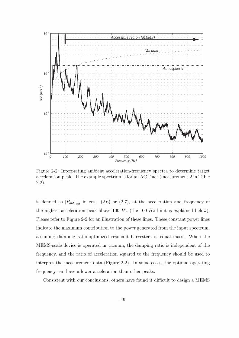
0 100 200 300 400 500 600 700 800 900 100010
-4
10-3
10-2
10-1
Frequency [Hz]
Acc
[m
/s2]
Accessible region (MEMS)
Atmospheric
Vacuum
Figure 2-2: Interpreting ambient acceleration-frequency spectra to determine targetacceleration peak. The example spectrum is for an AC Duct (measurement 2 in Table2.2).
is defined as |Pout|opt in eqs. (2.6) or (2.7), at the acceleration and frequency of
the highest acceleration peak above 100 Hz (the 100 Hz limit is explained below).
Please refer to Figure 2-2 for an illustration of these lines. These constant power lines
indicate the maximum contribution to the power generated from the input spectrum,
assuming damping ratio-optimized resonant harvesters of equal mass. When the
MEMS-scale device is operated in vacuum, the damping ratio is independent of the
frequency, and the ratio of acceleration squared to the frequency should be used to
interpret the measurement data (Figure 2-2). In some cases, the optimal operating
frequency can have a lower acceleration than other peaks.
Consistent with our conclusions, others have found it difficult to design a MEMS
49

device with a resonant frequency below 100 Hz (as size scales down, resonant fre-
quency increases) [5]. The lower limit for practical vibration peaks has been set to
100 Hz for the current investigation, thus defining the “accessible region” above 100
Hz, as in Figure 2-2.
Two other schemes for the interpretation of the measurement data have been put
forward in the literature. In the first, the peak power generated is written as in
eq. (2.3) (with Ω = 1), but the frequency dependence of the damping term is not
considered [30, 5]. In the second scheme, the power generated is written in terms of
both the input and output parameters, which can be simplified to obtain eq. (2.3)
(with Ω = 1), and similarly does not account for the damping-frequency dependence
for a MEMS device [72].
2.4 Power Available from Ambient Vibrations (Sum-
mary of Experimental Results)
In order to better understand the characteristics of low-level ambient sources, vibra-
tions measurements for a variety of everyday objects were taken. The purpose of
the measurements was to get an indication of the frequency range and amplitude of
vibrations from these sources. Eight separate sources under different conditions were
analyzed (14 cases in total), over the frequency range 10 – 1, 000 Hz. Details of the
sources/conditions and the experimental procedures are given in Appendix A.
The interpretation schemes for input vibration frequency selection from Section
2.3 is used. It was found that macro- and micro-systems require separate schemes
since the dominating damping mechanisms for these systems vary. This is in contrast
to previous findings where the mechanisms of the damping were ignored and/or as-
sumed independent of frequency. For micro devices, the operating environment will
further influence the selection of a vibration frequency to target. Lastly, ambient
vibration sources generally exhibit multiple peaks of significant power. This observa-
tion motivated an investigation into the effect of higher device resonance modes on
50

the power generation and static failure of the structure in Section 2.5.1.
The interpretation scheme for a MPVEH device operated under atmospheric con-
ditions, |Pout|opt ∝ w2B, discussed in Section 2.3, is used to identify three acceleration
peaks for each source, and are listed in Table 2.2. The first peak has the maximum
power content (e.g., the highest acceleration squared) and is referred to as the “High-
est Peak”, or HP. The “Reference Peak”, RP, is the highest acceleration peak in the
accessible region (i.e., above 100 Hz). The “Alternate Peak”, AP, is a secondary peak
in the accessible region. For some of the sources, the HP and the RP coincide. It
can be seen that the ranges and levels of ambient vibrations vary greatly: for HP,
the levels varied from 10−3 m/s2 to around 4 m/s2. However, not all these peaks
are accessible (e.g., above 100 Hz), and RP values range from 10−4 m/s2 to 4 m/s2.
At this time, the efficiency of power conversion is not known for the various energy
harvesters and a minimum vibration level required for positive power generation has
not been established. The measured spectra show good agreement with published
ambient vibration data [5].
Upon comparing RP and AP values, two important observations are made. Firstly,
in 7 of the 14 cases investigated, an AP was identified at a lower frequency than the
RP. The significance of this becomes clear when the device is operated in vacuum.
As is illustrated in Figure 2-2, the constant power lines for a device operated in
vacuum tends to zero as the frequency decreases. In other words, the acceleration
amplitude required at low frequencies for a constant power tends to zero since the
power is inversely proportional to the frequency. From the example it is clear that
the AP will have the same power content as the RP (refer to Figure 2-2). If the
operating environment is vacuum, the optimal harvesting point for a MEMS-scale
beam harvester might not correspond to the highest vibration level peak (RP as
defined here), but will be at a lower acceleration amplitude and frequency. A reference
vibration of wB = 2.5 m/s2 at 150 Hz (approximately vibrations measured on a
microwave oven side panel) is used for the preliminary design of an MPVEH in Section
6.4.
51

Table 2.2: Summary of measured ambient vibration sources: quantitative comparisonfor harvester operated in atmospheric conditions.
HPP RP AP
# Source† Acc.
[m/s2]
Freq.
[Hz]
Acc.
[m/s2]
Freq.
[Hz]
Acc.
[m/s2]
Freq.
[Hz]
1 A/C duct: center, low 0.0328 15.7 0.0254 171.9 0.0130 113.8
2 A/C duct: side, high 0.0990 53.8 0.0159 170.6 0.0127 98.8
3 A/C duct: center, high 0.0398 55.0 0.0366 173.1 0.0186 108.3
4 Computer side panel 0.0402 276.3 0.0402 276.3 0.0360 120.0
5 Microwave oven: top 1.11 120.0 1.11 120.0 0.570 240.0
6 Microwave oven: side 4.21 148.1 4.21 148.1 1.276 120.0
7 Office desk 0.0879 120.0 0.0879 120.0 0.00516 546.3
8 Harvard bridge railing 0.0215 171.3 0.0215 171.3 0.0193 136.3
9 Parking meter: Perp. 0.0327 13.8 0.00172 120.0 0.000697 148.1
10 Parking meter: Par. 0.0355 13.8 0.00207 923.8 0.000509 977.5
11 Car hood: 750 rpm 0.0744 35.6 0.0143 148.8 0.0103 510.6
12 Car hood: 3000 rpm 0.257 147.5 0.257 147.5 0.102 880.6
13 Medium tree 0.000985 16.3 0.000229 115.3 0.000226 240.0
14 Small tree 0.003 30.0 0.000465 293.1 0.000425 99.4
† See Appendix A for a detailed description of sources and experiments.
2.5 Other Design Considerations
Since the vibration source signals do not in general contain only one frequency compo-
nent, it is possible to excite some of the higher order vibration modes of the structure.
The effect of the the higher order modes are investigated next. Also, high quality
factors are obtainable with MEMS-devices. The effects of the quality factor on the
system response is analyzed, with important design and system implications.
2.5.1 Higher-Order Modes
Some sources exhibit peaks with comparable power content at much higher frequen-
cies. See, for example, source 12 (Car hood at 3000 rpm) in Table 2.2. The higher
52

frequency peak can excite a second or third resonance mode of the structure and
strain cancellation (and therefore power reduction) in the harvester device is possi-
ble. The example has a reference peak of amplitude 0.257 m/s2 at 148 Hz, and an
alternate peak at 881 Hz with an acceleration of 0.102 m/s2. This finding prompted
an investigation into the effect of higher frequency modes of the beam structure when
aligned to an alternate peak of the source vibration.
As an example, a simple cantilever beam was modeled with the first resonance
frequency at 140 Hz and the second resonance frequency at 875 Hz. Thus, with
the variability of vibration sources, it is possible for the source alternate peak and
the second resonance peak of the beam to align. To investigate strain cancellation
for this simple cantilever, a modal analysis of the device with two input vibration
components was conducted. The first component was aligned with the first resonance
of the device (as would occur per design), and the second component coincided with
the second resonance of the beam. The vibration level of the second frequency com-
ponent was varied to analyze the effect on the developed strain as an indication of
power converted. Please refer to Figure 2-3 for strain vs. beam length under these as-
sumptions. The power of the second (or alternate) input peak is zero, half, and equal
to the power of the reference peak, respectively. The strain developed over the first
region of the beam (near the base) increases with the additional excitation (second
mode), whereas the strain is reduced towards the tip. Assuming that the power is
proportional to strain, it is necessary to look at the total area under the strain curve.
Since the second mode causes the total area to decrease, the total power will decrease
as well (assuming that the electrodes cover the whole surface). It is also possible to
identify an optimal electrode length in the region where the strain is increased, but
that is not affected by the cancellation of strain, for this simple case. Furthermore,
the second mode contributes by increasing the maximum developed strain at the base
of the beam, affecting the static failure design of such devices. For the purpose of
the analysis in this section, it is assumed that the mode deflections due to the two
inputs are in phase. Should this not be the case, a different final strain distribution
will be obtained, but the important conclusion is that strain cancellation is possible
53

-1.2
-1
0
Position
No
rma
lize
d S
tra
inP
AP = 0
PAP
= PRP
/2
PAP
= PRP
Power Benefit Strain cancelation (power loss)
L0
0-1
0
1Normalized mode shapes
No
rma
lize
d d
isp
lace
me
nt
L
Figure 2-3: Strain distribution for a beam excited by multiple input vibration com-ponents, illustrating net power loss.
when higher vibration modes are excited.
2.5.2 High Quality Factor Devices
Four dominating damping components were identified in Section 2.3 for a MEMS-scale
device. These were the drag force (airflow force), squeeze force, support losses, and
structural damping (defined in eqs. (2.9) – (2.12)). It was shown that for MEMS de-
vices, the dominant damping component depends on the operating environment (e.g.,
vacuum or atmospheric conditions). When these devices are packaged in vacuum, ex-
54

tremely high quality factors are obtainable. Quality factors of tens of thousands have
been reported for such MEMS resonators [73, 74, 75, 76]. The quality factor is sig-
nificantly reduced when the device is operated in air. Pourkamali et al. reports a
resonator with a quality factor of 300 in air, compared to 1800 for the same resonator
operated in vacuum [77]. Under vacuum conditions, the dominant damping terms are
the support losses and the structural damping.
The quality factor determines the response of the device to the input around the
resonance frequency. At resonance (Ω = 1), and with no electrical damping (ζe =
0), the displacement is related to the quality factor (and the mechanical damping)
through eq. (2.15).
|z| =MwB
K
1
2ζm=MwB
KQ (2.15)
MwB
Kis the static deflection. The amplification factor, defined in eq. (2.2), reduces
to the quality factor, (Q = 12ζm
), at resonance. Refer to Figure 2-4 for an illustration of
the effect of the quality factor on the system response. The quality factor determines
the amplification of the input (static deflection) by the device at resonance. The
quality factor can also be defined in terms of the peak width at the half-power points:
ζm = Ωa−Ωb
2[78]. The half-power points are defined at the frequencies where the
maximum amplification is reduced by a factor of 1√2, or about 70.7 %. These points
have been included in Figure 2-4 for the quality factors of 100 and 500 respectively.
A high quality factor results in a very large amplification of the input and a very
narrow peak. The response decreases rapidly away from the peak frequency. These
effects on the response of the system have different design implications, which will be
discussed next.
The first implication is that the quality factor determines the displacement for the
structure around resonance. For a beam in bending, the strain is directly related to
this displacement and the strain determines the power generated by a piezoelectric
energy harvester. Thus, the higher the quality factor, the higher the power generated
for a given input. The effect of the quality factor on the power can also be seen in eq.
(2.6). Conversely, given a minimum power requirement, it is possible to determine
55

0.99 0.992 0.994 0.996 0.998 1 1.002 1.004 1.006 1.008 1.010
50
100
150
200
250
300
350
400
450
500
Normalized frequency, Ω
Am
plif
ica
tion
fa
cto
r |G
(iω)|
Q = 500Q = 400Q = 300Q = 200Q = 100
Half power points for Q = 500
Half power points for Q = 100
Ωa Ωb
Figure 2-4: Effect of quality factor on system response: displacement magnitude vs.normalized frequency.
the minimum input necessary to generate that power with a device with a known
quality factor, using eq. (2.6).
Secondly, the quality factor will determine the width of the response peak. For
resonating harvesters, the objective is to align the resonance frequency of the device
with the optimal source vibration peak (which was identified in Section 2.3). When
the quality factor is very high, the response peak is very narrow. Thus, if the input
peak and resonance frequency of the device are perfectly aligned, the power gener-
ated will be high. However, when the alignment of these peaks deviate even slightly,
the power extracted from the system will decrease dramatically. As a result, incor-
porating a tuning mechanism into the device may be desirable, or even necessary.
A possibility to accomplish resonant frequency tuning is with a variable capacitor
[79], though it is not in the scope of the this project to investigate the mechanism
56

further. For the variable capacitor, the lateral deflection of the resonator will change
the bending stiffness of the structure, thus changing the resonance frequency. The
disadvantage is that this mechanism consumes power. A trade-off study will be nec-
essary to determine the range of tunability achievable and the electrical cost vs. the
increased power generation. A second motivation for investigating the tuning mecha-
nism is the variability of current MEMS manufacturing processes. MEMS fabrication
processes can have high variability (up to 10% variation in dimension transfer from
the mask to the wafer for some photolithography processes). As a result, the resonant
frequency cannot be controlled as accurately as desired. This variability may make a
tunable device a necessity.
2.6 Design Implications for a MPVEH
Previous research has mostly focused on macro-scale harvesting devices. Three mech-
anisms of vibration to electrical energy have been investigated, and utilizing the
piezoelectric effect appears to be superior. Ambient sources were measured, and har-
vestable levels of vibration were identified below 300 Hz. From the dissipative 1-D
model, it was shown that the mass of the resonating structure should be maximized,
while the stiffness should be minimized (eq. (2.7)). This can be accomplished through
material selection and changing the device geometry. For example, the cantilevered
beam structure (used in this project) is very compliant and yet simple to analyze
and compatible with MEMS fabrication processes. Modal beam models are needed
to investigate the effect of higher resonance modes on the power generation and the
failure of the device. Furthermore, the damping in the system should be minimized
(the quality factor, Q, should be maximized). MEMS devices have the advantage
that extremely high Q’s are achievable. A high Q implies a narrow response peak
and high input amplification around the resonance. The narrow peak may require
the implementation of a tuning mechanism so that the resonance frequency of the
device is controllable. This is due to the rapid reduction in the power generated
when the resonance frequency of the device and the input vibration peak are not
57

perfectly aligned. MEMS configurations also impose a lower limit on the resonance
frequency (around 100 Hz). This is because the resonant frequency scales up as size
scales down. Thus, the target frequency range has been set to 100 – 300 Hz. MEMS
devices (with high Q’s) will enable ambient vibration energy harvesting since the high
Q’s will reduce the minimum vibration input amplitude required to generate a use-
able level of power. Lastly, one of the advantages of MEMS fabrication is the ability
to add additional harvesting structures to a device (as the footprint area allows) at
negligible additional cost. By interconnecting the individual harvesters in series or
parallel (or combinations thereof), the electrical output (voltage and current) from
the complete device can be controlled. This will allow maximization of power per
unit area and the tailoring of the electrical output for a specific application.
58

Chapter 3
Piezoelectric Energy Harvester
Models
Coupled electromechanical models are developed for design and performance predic-
tion of a micro-scale piezoelectric energy harvester and for validation to macro-scale
harvester experiments. A basic 1-D accelerometer-type closed-form model is shown
to characterize the behavior of beam configuration harvesters adequately by compar-
ison to more rigorous models based on a modal analysis. Uni-morph and bi-morph
beam configurations, as well as 3-1 and 3-3 actuation modes (the latter using
interdigitated electrodes) are considered. The modal analysis for the less common
beam geometry including a proof mass at the free end is also included.
3.1 The Piezoelectric Effect
In 1880, Jacques and Pierre Curie discovered the piezoelectric effect in certain crys-
talline materials: when these materials are subjected to a mechanical force, their
crystals become electrically polarized. The polarities for tensile and compressive
forces are opposite and the polarity is proportional to the applied force. The converse
relationship is also true: when the crystalline material is subjected to an electric field
it lengthens or shortens according to the polarity of the electric field. The latter
is known as the inverse piezoelectric effect. Please note that this section has been
59

adapted from [80, 81] and focusses on perovskite-type piezoceramics such as PZT
(lead zirconium titanate). In general, there is a distinction between piezoelectric and
ferroelectric materials. Materials with crystals that have a dipole are termed piezo-
electric materials. A subset of these materials, termed ferroelectric materials, can
be poled (i.e., the dipole direction can be changed). Poled ferroelectric materials
oftentimes exhibit stronger piezoelectric coupling than their un-poled counterparts
and are used in many actuation and sensing applications. Thus, to be consistent
with convention, reference to piezoelectric materials in this work will include poled
ferroelectric materials.
Bulk piezoelectric ceramics consist of multiple individual perovskite crystals. The
crystals are typically randomly oriented in the polycrystalline ceramic and are arranged
in grains with multiple domains in a grain. Each crystal consists of a small tetravalent
metal ion (titanium, zirconium, etc.) in a lattice of divalent metal ions (lead, barium,
etc.) and O2 - ions. Above a critical temperature (the Curie point), the crystals have
a simple cubic symmetry with no dipole moment and no piezoelectric effect. However,
below this temperature, the metal ions are displaced and the crystals lose their cu-
bic structure. The crystals obtain a tetragonal symmetric structure and each crystal
has a dipole moment (also referred to simply as a dipole, or remnant polarization).
The cubic (non-piezoelectric) and tetragonal (piezoelectric) single crystal structures
of perovskite ceramics are shown in Figure 3-1.
Adjoining dipoles form regions of local alignment and are called domains. These
domains, like the crystals that comprise them, possess net dipole moments, result-
ing in a net polarization. The directions of polarization among neighboring domains
and grains in the bulk are random and the ceramic has no overall polarization. The
piezoelectric element as a whole is exposed to a strong electric field, (∼ 1 kVmm
[66]),
usually at a temperature slightly below the Curie point. This is referred to as the
“poling” of the ferroelectric to create a ceramic with strong piezoelectric coupling.
The randomly-oriented domain dipoles become somewhat aligned with the strong
electric field and the element expands in the direction of the field. This expansion
is an artifact of the crystals (with the tetragonal crystal structures) that are not in
60

(+)
(-)
P
a) Temperature above Curie temperature: cubic lattice, symmetric arrangement of positive and negative charges
b) Temperature below Curie temperature: tetrtagonal lat- tice, crystal has electric dipole
A2+ = Pb, Ba, other large divalent metal ion
O2- = Oxygen
B4+ = Ti, Zr, other similar tetravalent metal ion
Figure 3-1: Cubic and tetragonal crystal structure of a traditional perovskite (ABO3)ceramic, such as PZT.
random orientations anymore, but are better aligned with the electric field. When
the electric field is removed, many of the dipoles are locked into the configuration
of near alignment, primarily due to domain wall motion which occurs during poling.
The ceramic now has a permanent polarization, the bulk remnant polarization, and
is permanently elongated. Examples of ferroelectric materials with high piezoelec-
tric coupling are PZT (lead zirconate titanate) and BaTiO3 (barium titanate), as
compared to ZnO (zinc oxide), which is a piezoelectric material with relatively little
piezoelectric coupling.
Individual crystals of a piezoelectric (such as those described above) have large
piezoelectric coupling coefficients relative to the bulk, randomly oriented poly-crystalline
form of piezoelectrics typically encountered (such as PZT). The reduction in coupling
in the bulk form is due to misalignment of domains relative to the poling axis and
incomplete lock-in of poled crystals. Calculations can be made of the degree of in-
complete lock-in based on measured piezoelectric coupling in the bulk ceramic vs.
the single crystal form [82]. Thin films of piezoelectrics, including PZT, oftentimes
are formed with a preferred texture (tetragonal axis is aligned with out-of-plane film
axis) along the normal to the film depending on the processing employed. In-plane
texture in the thin-film plane, however, is random. Regardless of the texture of the
film, the piezoelectric and elastic constants can be formulated and measured based
61
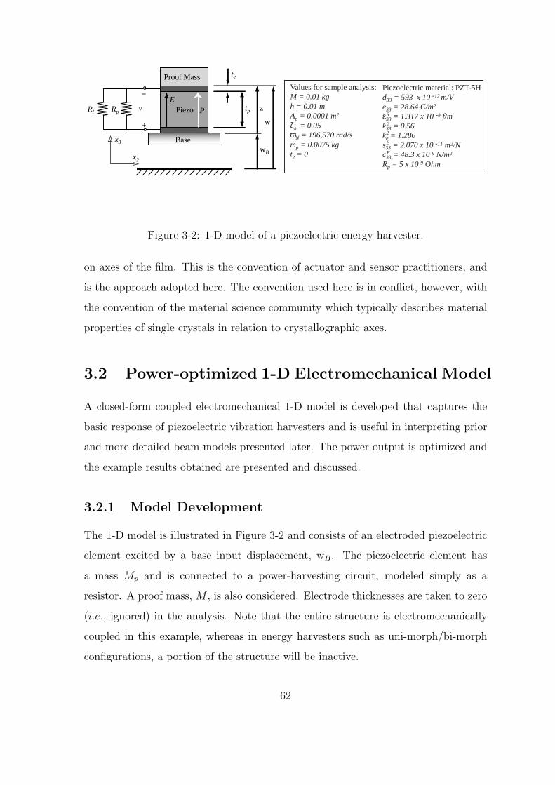
tp z
wB
+
Rl
-
Base
Piezo
Proof Mass
vRp
x3
x2
te
Values for sample analysis: M = 0.01 kg h = 0.01 m Ap = 0.0001 m2 ζm = 0.05 ωN = 196,570 rad/s mp = 0.0075 kg te = 0
Piezoelectric material: PZT-5H d33 = 593 x 10 -12 m/V e33 = 28.64 C/m2 ε33 = 1.317 x 10 -8 f/m k33 = 0.56 ke = 1.286 s33 = 2.070 x 10 -11 m2/N c33 = 48.3 x 10 9 N/m2 Rp = 5 x 10 9 Ohm
S
2
2
E
E
P
E
w
Figure 3-2: 1-D model of a piezoelectric energy harvester.
on axes of the film. This is the convention of actuator and sensor practitioners, and
is the approach adopted here. The convention used here is in conflict, however, with
the convention of the material science community which typically describes material
properties of single crystals in relation to crystallographic axes.
3.2 Power-optimized 1-D Electromechanical Model
A closed-form coupled electromechanical 1-D model is developed that captures the
basic response of piezoelectric vibration harvesters and is useful in interpreting prior
and more detailed beam models presented later. The power output is optimized and
the example results obtained are presented and discussed.
3.2.1 Model Development
The 1-D model is illustrated in Figure 3-2 and consists of an electroded piezoelectric
element excited by a base input displacement, wB. The piezoelectric element has
a mass Mp and is connected to a power-harvesting circuit, modeled simply as a
resistor. A proof mass, M , is also considered. Electrode thicknesses are taken to zero
(i.e., ignored) in the analysis. Note that the entire structure is electromechanically
coupled in this example, whereas in energy harvesters such as uni-morph/bi-morph
configurations, a portion of the structure will be inactive.
62

Using the 1-D configuration, we can simplify the 3-D linear elastic (small-signal)
constitutive relations [83, 84] in eq. (3.1) to eqs. (3.2) and (3.3):
T
D
=
cE −et
e εS
S
E
(3.1)
T3 = cE33S3 − e33E3 (3.2)
D3 = e33S3 + εS33E3 (3.3)
The D, E, S, and T matrices are defined as developed electric displacement,
applied electric field, applied strain, and developed stress, respectively. The reader is
referred to Appendix B for the sign convention of the electrical parameters used in
this work. ε is the permittivity of the piezoelectric element and e is the piezoelectric
constant relating charge density and strain and is defined as positive in the direction
indicated (the element local coordinates coincide with the global coordinates). The
poling direction of the piezoelectric element defines the element’s local coordinate
system, and the piezoelectric constant needs adjustment (sign correction) when the
element local coordinates does not coincide with the global coordinates. The treat-
ment of poling direction and the piezoelectric constant is discussed in Appendix B,
and [85, 86]. e is also referred to as the piezoelectrically induced stress tensor as it
relates the stress to electric field. cE is the stiffness matrix. The superscripts E and S
indicate a parameter at constant (typically zero) electric field and strain respectively,
while superscript t indicates the transpose of the matrix. For the analysis in later
sections, the superscripts D and T indicate a parameter at constant (typically zero)
electric displacement and stress, respectively. Note that cE33 in the 1-D model would
be measured under short circuit conditions, i.e., by connecting the electrodes on the
piezoelectric block.
From a force equilibrium analysis, the governing equations can be found in terms
of the constitutive relations (eqs. (3.2) and (3.2)) and device parameters, defined in
Figure 3-2. The piezoelectric element is poled in the x3 direction. The strain is related
to the device parameters through S3 = ztp
and the electric field is defined as E3 = − vtp
.
63

z is the relative displacement, as in Figure 3-2. The approximate total mass1 of the
system is MT = M + 13Mp and me = MT
Apis the mass per cross-sectional area. Ap is
the area of the electrodes (or the piezoelectric element). The stress is the force per
area, or T3 = −MT (z+wB)Ap
= −me (z + wB). wB is the base acceleration and q is the
charge developed on the electrodes. The overhead dot indicates the time derivative of
the variable. The electric displacement, D3, is the charge on the electrodes per unit
area. This all gives:
mez + cE33z
tp+ e33
v
tp= −mewB (3.4)
D3 = e33z
tp− εS
33
v
tp=
q
Ap
(3.5)
Both equations are multiplied by Ap and a convenient electromechanical coupling
term, θ = − e33Ap
tp, is defined. Furthermore, K =
cE33
Ap
tpis the effective stiffness. The
capacitance is defined in terms of the constrained permittivity: Cp =εS33
Ap
tp. The
overhead dot indicates the time derivative. The second governing equation (sensing
equation), eq. (3.5), can be written in terms of the current, i = dq
dt, by taking the
time derivative. For the purely resistive electrical load (as has been assumed), the
current can be related to the voltage developed through v = iRpar. The equivalent
resistance, Rpar, is the parallel resistance of the load and the leakage resistances, Rl
and Rp respectively. In general, the leakage resistance is much higher than the load
resistance [87], so that Rpar ≈ Rl. With these definitions and substitutions, eqs. (3.6)
and (3.7) are obtained from eqs. (3.4) and (3.5).
MT z +Kz − θv = −MT wB (3.6)
θz + Cpv +1
Rl
v = 0 (3.7)
Note that eq. (3.6), without the θv coupling term, is the familiar dynamic equa-
tion of motion for a 1 degree-of-freedom spring-mass system. Eq. (3.6) can be further
reduced by dividing through by the approximate total mass, MT , and using the defini-
1For longitudinal vibrations of a rod, the resonance frequency is often estimated by lumping onethird of the mass of the rod at the tip. Together with the proof mass, this defines an approximateeffective mass for the system.
64

tion for the resonance frequency, ω2N = K
MT=
cE33
metp. Note that ωN , due to the fact that
the structure is a piezoelectric block, is related to the speed of sound (or a pressure
wave) through the piezoelectric material at short circuit (E = 0) conditions. Viscous
damping (proportional to velocity, z) is added through the mechanical damping ratio,
ζm, so that eq. 3.6 becomes:
z + 2ζmωN z + ω2Nz − θ
MT
v = −wB (3.8)
Using Laplace transforms, the governing equations can be evaluated and the mag-
nitudes of the relative displacement, voltage, and electrical power extracted can be
determined. These are given in eqs. (3.9) – (3.11), normalized by the input force
(MT wB). The dimensionless parameter Ω = ωωN
and electromechanical coupling coeffi-
cient, k2e =
k2
33
1−k2
33
=e2
33
cE33
εS33
, can be defined [81, 82]. k233 =
d2
33
sE33
εT33
is the electromechanical
coupling coefficient relating converted electrical energy to input mechanical energy, or
vice versa, for the 1-D system. Lastly, the dimensionless time constant of the system,
α = ωNRlCp, is defined. RlCp is the time constant of the electrical circuit, while 1ωN
is related to the period of the mechanical resonator.
∣
∣
∣
∣
z
MT wB
∣
∣
∣
∣
=1
K
√
1 + (αΩ)2
√
[1 − (1 + 2ζmα) Ω2]2 + [(2ζm + (1 + k2e)α) Ω − αΩ3]2
(3.9)
∣
∣
∣
∣
v
MT wB
∣
∣
∣
∣
=1
|θ|αk2
eΩ√
[1 − (1 + 2ζmα) Ω2]2 + [(2ζm + (1 + k2e)α) Ω − αΩ3]2
(3.10)
∣
∣
∣
∣
Pout
(MT wB)2
∣
∣
∣
∣
=ωN
K
αk2eΩ
2
[1 − (1 + 2ζmα) Ω2]2 + [(2ζm + (1 + k2e)α) Ω − αΩ3]2
(3.11)
3.2.2 Power Optimization
In all known prior energy harvester work, eqs. (3.9) – (3.11) are simplified by setting
Ω = 1, which will be shown to miss important features of the coupled response
(particularly anti-resonance). It is of interest to optimize the power extracted from the
source. Again, taking the leakage resistance as much larger than the load resistance
65

(Rpar ≈ Rl), the power can be optimized with respect to the load resistance, Rl,
or equivalently with respect to the dimensionless parameter, α. In performing this
optimization, it is convenient to first expand the denominator in powers of α. The
result gives:
α2opt =
Ω4 + (4ζ2m − 2) Ω2 + 1
Ω6 + (4ζ2m − 2 [1 + k2
e ]) Ω4 + [1 + k2e ]
2 Ω2=
1
Ω2
(1 − Ω2)2 + (2ζmΩ)2
([1 + k2e ] − Ω2)2 + (2ζmΩ)2
(3.12)
This αopt gives the load resistance, Rl, to extract maximum power at any frequency
ratio, Ω. The corresponding power generated is found by substituting the αopt back
into the power expression, eq. (3.11). Since a piezoelectric element exhibits both
open- and short-circuit stiffness, there will be two important optimal-power operating
frequencies to consider. First, set ζm = 0 and let Rl → 0 in eq. (3.9) to obtain the
short-circuit natural frequency:
Ωr = 1 or, ωr =
√
cE33Ap
MT tp(3.13)
This has previously been defined as the resonance frequency, ωN . This frequency
is defined at the minimum impedance of the circuit [82, 84]. For the open-circuit
analysis, set ζm = 0 and let Rl → ∞ in eq. (3.9) to obtain the open-circuit natural
frequency:
Ωar =√
1 + k2e =
1√
1 − k233
or, ωar =
√
cD33Ap
MT tp(3.14)
This frequency is known as the anti-resonance frequency and is defined at the
maximum impedance of the circuit [82, 84]. The ratio of the anti-resonance to reso-
nance frequency (Ωar) is governed solely by the electromechanical coupling coefficient
(k233 or k2
e) for this case where the entire structure is coupled. Finally, a system cou-
pling factor is often defined in terms of the resonance and anti-resonance frequencies
as k2sys = Ω2
ar−Ω2r
Ω2ar
[57, 84]. For this 1-D case, where the entire structure is made up
of a piezoelectric, this system coupling factor is related to the other coupling factors
through: k2sys = k2
33 = k2e
1+k2e. Note that Ωar ≥ Ωr since the coupling is always positive
66

or zero. Using these frequency ratios, it is possible to obtain optimal resistances with
eq. (3.12) under the respective operating conditions. First, the optimal electrical
loading at resonance (Ωr) is determined:
α2opt,r =
4ζ2m
4ζ2m + k4
e
(3.15)
ζm is generally at least an order of magnitude smaller that k2e , thus this result can
be approximated very well as:
αopt,r ≈2ζmk2
e
(3.16)
This result, with Ω = Ωr = 1, can be substituted into eq. (3.11) to obtain
maximum normalized power at resonance:
∣
∣
∣
∣
Pout
(MT wB)2
∣
∣
∣
∣
opt,r
=ωN
K
2ζm
16ζ2m
(
ζ2m
k2e
+ 1) (3.17)
The term in the denominator, ζ2m
k2e≪ 1, such that this result reduces to eq. (3.18):
∣
∣
∣
∣
Pout
(MT wB)2
∣
∣
∣
∣
opt,r
=ωN
K
1
8ζmor |Pout|opt,r =
(MT )32
√
cE33
Ap
h
w2B
8ζm(3.18)
A parallel approach is to substitute eq. (3.16) into the voltage developed, eq.
(3.10), which then reduces to |v|opt,r = MT wB
2|θ| . The power is related to the voltage
developed and the electrical load (purely resistive) through |Pout|opt,r =|v|2opt,r
Rlr. The
optimal resistance is Rlopt,r ≈ 2ζm
k2e
1ωNCp
using eq. (3.16). Substituting these into the
optimal power equation defined above, eq. (3.18) is obtained, as expected.
A similar analysis can be completed at the anti-resonance frequency ratio, Ωar.
The anti-resonance frequency is determined by the coupling term, as seen in eq.
(3.14). Substituting this result into eq. (3.12), the following is obtained:
α2opt,ar =
(1 + k2e)
2 − 2(1 + k2e) + 1 + 4ζ2
m(1 + k2e)
4ζ2m(1 + k2
e)2
(3.19)
67

The last term in the numerator will be much smaller than the other terms. The
result can be simplified to:
αopt,ar ≈k2
e
2ζm(1 + k2e)
(3.20)
Again, this result and Ω = Ωar can be substituted into the power expression, eq.
(3.11).∣
∣
∣
∣
Pout
(MT wB)2
∣
∣
∣
∣
opt,ar
=ωN
K
12ζm
k4e
4k4e + 4ζ2
m (1 + k2e)
(3.21)
The second term in the denominator will be much smaller than the first due to the
small damping and eq. (3.21) reduces to eq. (3.18). This is a very surprising result.
The piezoelectric coupling, represented by k2e , cancels from the power equations at
optimal conditions, both at resonance and anti-resonance (provided that ζm ≪ k2e).
First, this would suggest that the power generated at the resonance and anti-resonance
frequencies are equal (under optimal conditions). Next, the only material properties
that would then influence the power generated are the piezoelectric element short-
circuit stiffness, cE33, and the density (of the mass and the piezoelectric element). As
with the resonant frequency voltage optimal, the voltage optimal at anti-resonance is
a function of the piezoelectric coupling and αopt,ar through |v|opt,ar = MT wB
2|θ| αopt,ar =
|v|opt,r αopt,ar. These results will be discussed in greater detail for the coupled beam
model in Section 3.3.
3.2.3 1-D Model Results
It should be noted that the above model assumes linear behavior of the piezoelectric
element over all frequencies. This is not the case for known piezoelectric materials;
particularly the impedance (R − C) of the piezoelectric deviates significantly from
non-resonant values at material resonance and anti-resonance [81, 82]. The power
optimization and solutions here are relevant to understanding power optimums of
structural elements (beams) with piezoelectric elements, but not prediction due to
unmodeled effect.
Power is plotted against normalized frequency in Figure 3-3 for the parameters
68

0.4 0.6 0.8 1 1.2 1.4 1.6 1.80
2
4
6
8
10
12
14
16
Ω [Dimensionless]
Po
we
r o
ut [m
W]
Rl,r = 2995 OhmRl = 10000 OhmRl = 25000 OhmRl = 80000 OhmRl,ar = 218771 OhmRl,opt
Figure 3-3: Power vs. normalized frequency with varying electrical resistance for 1-Dmodel in Figure 3-2. Rl is the electrical load resistance, Rl,r and Rl,ar are the poweroptimized electrical loads at resonance and anti-resonance, respectively. The solidline is the optimized power (optimal electrical load, Rl,opt, at all frequencies).
given in Figure 3-2 with a base input acceleration of 9.81 m/s2, or 1 g. Note that
Ωar ≈ 1.5 here. The solid line forms the envelope of maximum power possible if the
electrical resistance (Rl) is optimized at each frequency ratio. Switching between the
two peaks, corresponding to the resonance and anti-resonance frequencies, is achieved
by varying the electrical load. The power increases as the resonance frequency is
approached, and reaches a maximum, before decreasing to a local minimum at Ω ≈1.25. This local minimum corresponds to a local minimum in proof mass displacement.
The power then increases to a second maximum, corresponding to the anti-resonance
frequency. Note the sharpness of the tuned peaks around the two natural frequencies.
69

0.4 0.6 0.8 1 1.2 1.4 1.6 1.80
0.2
0.4
0.6
0.8
1
1.2
Ω [Dimensionless]
Dis
pla
cem
en
t [n
m]
Rl,r = 2995 OhmRl = 10000 OhmRl = 25000 OhmRl = 80000 OhmRl,ar = 218771 OhmRl,opt
Figure 3-4: Displacement vs. normalized frequency with varying electrical resistancefor 1-D model in Figure 3-2. Rl is the electrical load resistance, Rl,r and Rl,ar are thepower optimized electrical loads at resonance and anti-resonance, respectively. Thesolid line is the optimized power (optimal electrical load, Rl,opt, at all frequencies).
A higher mechanical damping ratio would broaden, but also lessen, these peaks. While
the extracted powers predicted at these peaks are equal, the voltage and current differ
significantly.
Next, the relative displacements of the proof mass at the two peaks are compared,
as shown in Figure 3-4. The electrical resistance is still optimized for maximum power.
Unlike the power, the displacement is higher at resonance than at anti-resonance.
Also note that the relative displacement of the proof mass is not locally minimized
at either the resonance or the anti-resonance peak (where the power extracted is
maximized), but at an intermediate position. Operating at the second peak could
70

0.4 0.6 0.8 1 1.2 1.4 1.6 1.80
0.2
0.4
0.6
0.8
1
1.2
1.4
1.6
1.8
Ω [Dimensionless]
Vo
ltage
[V
]
Rl,r = 2995 OhmRl = 10000 OhmRl = 25000 OhmRl = 80000 OhmRl,ar = 218771 OhmRl,opt
Figure 3-5: Voltage vs. normalized frequency with varying electrical resistance for1-D model in Figure 3-2. Rl is the electrical load resistance, Rl,r and Rl,ar are thepower optimized electrical loads at resonance and anti-resonance, respectively. Thesolid line is the optimized power (optimal electrical load, Rl,opt, at all frequencies).
be advantageous since the proof mass displacement will be smaller, allowing for a
smaller device operating volume.
Voltage is plotted against normalized frequency in Figure 3-5. As with the dis-
placement, the voltage generated at the two resonances differ, but in the case of the
voltage the difference is around an order of magnitude. Since the power generated
at these peaks are the same, and power is related to voltage and current, i, through
Pout = vi (for a resistive load), the current at the first peak will be an order of
magnitude larger than at the second peak (inverse of voltage). The capability of a
piezoelectric element to charge a secondary battery has been investigated by Sodano
et al. [88]. From the study it was concluded that certain piezoelectric elements are
71

not well suited for battery charging applications, as generated current levels are too
low. Operation at the resonance frequency could potentially alleviate the problem.
On the other hand, the rectifier circuit has a minimum voltage requirement for op-
eration, and the voltage requirement is also governed by the onset of losses at lower
voltages [44]. Operating at the anti-resonance frequency could be advantageous in
this case.
The power-optimal load resistance is plotted against frequency ratio in Figure 3-6.
The shift from the resonance to anti-resonance frequencies is clearly observable. As
mentioned, the magnitude of Ωar is governed by the piezoelectric coupling, k2e . This
coupling is a function of the stiffness contribution of the piezoelectric element to the
device. In the 1-D model, the shift is most pronounced since the piezoelectric ele-
ment constitutes the entire structure (and thus the stiffness). The optimal frequencies
corresponding to the optimal electrical loads calculated for the resonance and anti-
resonance frequencies do not perfectly align with the resonance and anti-resonance
frequencies due to the finite mechanical damping in the system. For low damping,
these higher peaks will be negligibly offset from the resonance and anti-resonance fre-
quencies. In fact, for progressively higher damping cases, the maximum power peaks
shift towards each other, and the two optimal-power operating points (resonance and
anti-resonance for low damping) merge to a single peak at an intermediate frequency.
For this analysis, it has been assumed that the damping is relatively low (ζm = 0.005).
To summarize, as the electrical load is increased, the piezoelectric element op-
erating condition moves from short-circuit to open-circuit. Since the piezoelectric
element constitutes the whole structure, there is a significant shift in the resonance
frequency. For beams/plates at the macro-scale, this effect is not as pronounced since
the piezoelectric element generally does not contribute significantly to the overall
structural stiffness (e.g., for a piezoelectric patch applied to a structure for sensing).
Also, macro-scale structures normally have more significant damping. Resonance and
anti-resonance are very important at the micro-scale. The power generated at short-
and open-circuit conditions are equal (for constant acceleration amplitude and me-
chanical damping), but the voltage and current developed at the different operating
72

104
105
log
(Rl,o
pt)
[O
hm
]
Ω
[Dimensionless]
Rl,r = 2995 OhmRl = 10000 OhmRl = 25000 OhmRl = 80000 OhmRl,ar = 218771 Ohm
Ωr Ωar
Figure 3-6: Power-optimal resistive load vs. normalized frequency with varying elec-trical resistance for 1-D model in Figure 3-2.
points differ substantially. The displacement of the proof mass of the device is also
different at these operating points, as the system will have more damping at the
open-circuit condition (due to higher electrical damping).
3.3 Coupled Beam Models
As stated earlier, the cantilever beam configuration was chosen for its geometric
compatibility with the MEMS fabrication processes. It is also a relatively compliant
structure, allowing for large strains and thus more power generation. The basic
configurations of the uni-morph and bi-morph (for the 3-1 mode of operation) are
illustrated in Figure 3-7 and each have the following components: the cantilevered
73

e4
e3
e2
e1
v2
v1
Piezoelectric Layer
Structural Layer
Piezoelectric Layer
P
P
Electrodes
Bi-morph Configuration
e1
e2
v1
Piezoelectric Layer
Structural Layer
P
Electrodes
Uni-morph Configuration
L
b
tpts
Input: base excitation
Input: base excitation
+
+
+
_
_
_
xt
xa
Clamped boundary
Figure 3-7: Cantilever (top) uni-morph and (bottom) bi-morph configurations for3-1 operation. Refer to Appendix B for sign conventions used.
beam structure, piezoelectric elements, and electrodes. A proof mass can be added if
necessary.
In the section to follow, a coupled electromechanical model, based on a modal
analysis for a base-excited cantilever beam with a mass at the free end is developed.
A 3-1 actuation model of a typical uni-morph is developed and the model is then ex-
tended to a uni-morph configuration operating in the 3-3 actuation mode. Since the
poling direction, and thus the coordinate systems for the 3-1 and 3-3 models are
different, two general position variables are introduced, based on the beam structure
analyzed: xa indicates the axial position (along the length of the beam/structure),
and xt indicates the position through the thickness of the beam/structure (refer to
Figure 3-7, bottom).
74

3.3.1 Modeling Cantilever Beams with Piezoelectric Elements
The model for a cantilever beam with piezoelectric elements can be obtained with
an energy method approach. An alternative method, which will not be discussed in
this paper, is a force equilibrium analysis [89]. The analysis to follow was adapted
from Hagood et al. [85]. The generalized form of Hamilton’s Principle for an electro-
mechanical system, neglecting the magnetic terms and defining the kinetic (Tk), in-
ternal potential (U), and electrical (We) energies, as well as the external work (W ),
is given by:t2∫
t1
[δ (Tk − U +We) + δW ] dt = 0 (3.22)
δ indicates the first variation of the function, as used in Calculus of Variation. It
is not in the scope of this thesis to explain Calculus of Variation, as many texts on
the topic are available, for example [90]. The individual energy terms are defined as:
Tk =1
2
∫
Vs
ρsutu dVs +
1
2
∫
Vp
ρputu dVp (3.23)
U =1
2
∫
Vs
StT dVs +1
2
∫
Vp
StT dVp (3.24)
We =1
2
∫
Vp
EtD dVp (3.25)
The subscripts p and s indicate the piezoelectric element section and the structural
(inactive) section of the beam, respectively. Electrodes, each with thickness te, if
significant to the stiffness of the structure, can be included in the structural section
of the beam. Vp and Vs are volumes. The relative displacement is denoted by u (x, t)
and ρ is the density. The contributions to We due to fringing fields in the structure
and free space are neglected. nf discretely applied external point forces, fk (t) at
positions xk, and nq charges, qj, extracted at discrete electrodes with positions xj are
considered. The external work term is defined in terms of the relative displacement,
75
u (xk, t), and the scalar electrical potential, ϕj = ϕ (xj, t):
δW =
nf∑
k=1
δukfk (t) +
nq∑
j=1
δϕjqj (3.26)
The above definitions, as well as the small-signal constitutive relations of a piezo-
electric material (see eq. (3.1)), are used in conjunction with a Calculus of Variation
approach to rewrite eq. (3.22). It should be noted that it has been assumed that the
piezoelectric element local coordinates coincide with the global coordinates. The local
coordinates are defined by the poling direction, so according to this assumption, the
global coordinates are defined to align with the local coordinates and the constitutive
law as given in eq. (3.1) holds. Please refer to Appendix B for a scheme to account
for the inversion of the local piezoelectric element coordinates (negative poling).
t2∫
t1
(
∫
Vs
ρsδutu dVs +
∫
Vp
ρpδutu dVp −
∫
Vs
δStcsS dVs −∫
Vp
δStcES dVp +
∫
Vp
δStetE dVp+
∫
Vp
δEteS dVp +
∫
Vp
δEtεSE dVp +
nf∑
k=1
δukfk(t) +
nq∑
j=1
δϕjqj
)
dt = 0
(3.27)
Three basic assumptions are introduced: the Raleigh-Ritz procedure, Euler-Bernoulli
beam theory, and constant electrical field across the piezoelectric element. These
assumptions are consistent with previous modeling efforts (e.g., [55, 56, 85]). In the
Raleigh-Ritz approach, the displacement of a structure is written as the sum of nr
individual modes shapes, ψri (x), multiplied by a generalized mechanical coordinate,
ri(t) [91]. For a beam in bending, only the transverse displacement (xt direction)
is considered and the mode shape is a function only of the axial position, u (x, t) =
z (xa, t), as in eq. (3.28). Here, z(xa, t) is the beam displacement relative to the base of
the beam. Furthermore, the base excitation, wB, is assumed to be in the transverse
direction as well. Lastly, the electric potential for each of the nq electrode pairs
can be written in terms a potential distribution, ψvj, and the generalized electrical
76

coordinate, vj (t), as in eq. (3.29). It is convenient to let the generalized electrical
coordinates coincide with physical voltages, though this is not required [85]. The
Euler-Bernoulli beam theory allows the axial strain in the beam to be written in
terms of the beam neutral axis displacement and the distance from the neutral axis
(xt), as in eq. (3.30).
u (x, t) = z (xa, t) =nr∑
i=1
ψri(xa)ri(t) = ψr(xa)r(t) (3.28)
ϕ(x, t) =
nq∑
j=1
ψvj(x)vj(t) = ψv(x)v(t) (3.29)
S (x, t) = −xt
∂2z(xa, t)
∂x2a
= −xtψ′′rr(t) (3.30)
Primes indicates the derivative with respect to the axial position, xa. Next, the
above definitions are substituted into eq. (3.27) to yield:
t2∫
t1
(
∫
Vs
δrtψtrρsψrr dVs +
∫
Vp
δrtψtrρpψrr dVp −
∫
Vs
δrt(−xtψ′′r)
tcs(−xtψ′′r)r dVs−
∫
Vp
δrt(−xtψ′′r)
tcE(−xtψ′′r)r dVp +
∫
Vp
δrt(−xtψ′′r)
tet(−∇ψv)v dVp+
∫
Vp
δvt(−∇ψv)te(−xtψ
′′r)r dVp +
∫
Vp
δvt(−∇ψv)tεS(−∇ψv)
tv dVp+
nf∑
i=1
δrtkψ
tr,kf k +
nq∑
j=1
δvtjψ
tv,jqj
)
dt = 0
(3.31)
Using integration by parts, and noting that the variations must disappear at the
boundaries, the first two terms can be rewritten as∫
V
δrtρψtrψrr dV = −
∫
V
δrtψtrρψrr dVs.
Next, the terms are grouped and each variation (e.g., δrt and δvt), tend to zero sep-
77

arately. Two governing equations are obtained:
−∫
Vs
ψtrρsψrr dVs −
∫
Vp
ψtrρpψrr dVp −
∫
Vs
(−xtψ′′r)
tcs(−xtψ′′r)r dVs−
∫
Vp
(−xtψ′′r)
tcE(−xtψ′′r)r dVp +
∫
Vp
(−∇ψv)te(−xtψ
′′r)r dVp +
nf∑
i=1
ψtr,kfk = 0
(3.32)
∫
Vp
(−xtψ′′r)
tet(−∇ψv)v dVp +
∫
Vp
(−∇ψv)tεS(−∇ψv)
tv dVp +
nq∑
j=1
ψv,jqj = 0 (3.33)
From these equations, the mass (M), stiffness (K), coupling (Θ), and capacitive
matrices (Cp) are defined. Please refer to Appendix B for a detailed analysis of
the relationship between poling direction, piezoelectric constants, and applied and
developed electric fields.
M =
∫
Vs
ψtrρsψr dVs +
∫
Vp
ψtrρpψr dVp (3.34)
K =
∫
Vs
(−xtψ′′r)
tcs(−xtψ′′r) dVs +
∫
Vp
(−xtψ′′r)
tcE(−xtψ′′r) dVp (3.35)
Θ =
∫
Vp
(−xtψ′′r)
tet(−∇ψv) dVp (3.36)
Cp =
∫
Vp
(−∇ψv)tεS(−∇ψv) dVp (3.37)
The governing equations, given in eqs. (3.38) and (3.39), are obtained:
Mr +Kr − Θv =
nf∑
k=1
ψtr(xk)fk(t) (3.38)
Θtr +Cpv = −nq∑
j=1
ψv(xj)qj(t) (3.39)
78

The input to the system is a base excitation. To represent the beam’s inertial load
from this excitation, the structure is discretized into nf elements of length ∆xa and
the local inertial load is applied on the kth element, or fk = −mk∆xawB. This results
in nf discrete loads. mk is the element mass per length. The loading is summed for
all the elements. In the limit of ∆xa → dxa, the summation reduces to the integral
over the structure length and a mass per length distribution is used, m(xa). For
simplicity, it has been assumed here that the beam is of uniform cross-section in the
axial direction so that m(xa) = m = constant. Substituting the forcing function into
the right hand side of eq. (3.38), the “forcing vector”, Bf , is defined.
Bf =
L∫
0
m(xa)ψtrdxa = m
L∫
0
ψtrdxa (3.40)
The right hand side of eq. (3.39) reduces to a column vector, q, of length nq (the
number of electrode pairs) with element values qT (qT =nq∑
j=1
qj). This equation can
be differentiated with respect to time to obtain current. The current can be related
to the voltage, assuming that the electrical loading is purely resistive, Rl.
Mechanical damping is added through the addition of a viscous damping term, C,
to eq. (3.38) to obtain eq. (3.41). When multiple bending modes are investigated,
a proportional damping scheme is often used to ensure uncoupling of the equations
during the modal analysis [91]. The damping for a physical device is determined by
the geometry and the operating environment, as discussed in Section 2.3. Damping is
typically measured at the device natural frequency, which is fixed. As a consequence,
the damping dependence on frequency need not be considered here, if it can be
assumed that the damping ratios at the resonance and anti-resonance frequencies are
the same. The following results:
Mr +Cr +Kr − Θv = −Bf wB (3.41)
Θtr +Cpv + q = 0 (3.42)
79

It is important to note the similarities between the governing equations for the
vibrating beam eqs. (3.41) and (3.42) and the basic 1-D device eqs. (3.6) and (3.7).
Considering one beam mode and a single electrode pair, eqs. (3.41) and (3.42) re-
duce to scalar equations that allows for a beam power optimization to be performed,
directly analogous to the 1-D device derived in Section 3.2.2. The actuator equation,
eq. (3.41), is written in an alternative form by dividing through by M and making
use of the definitions for the first resonance frequency, ω1 =√
KM
, and damping ratio
ζm = C2Mω1
. Note that since one vibration mode (ψr,1) is considered, the system will
have a single natural frequency. For a piezoelectric structure, the natural frequency
will correspond to either the resonance or anti-resonance frequency, depending on the
electrical loading. ωN = ω1 corresponds to the resonance frequency. In the sensing
equation (eq. (3.42)), the charge can be related to the voltage through v = dq
dtRl = iRl
to obtain:
r + 2ζmω1r + ω21r − θ/Mv = −Bf wB/M (3.43)
θr + Cpv +1
Rl
v = 0 (3.44)
The dimensionless factors α = ω1RlCp, κ2 = θ2
KCp, and Ω = ω
ω1
are defined, where
ω is the base input frequency, and the system response is calculated. α is again the
dimensionless time constant and κ2 is a structure/system electromechanical coupling
coefficient, vs. k233 =
d2
33
sE33
εT33
or k2e =
e2
33
cE33
εS33
, which are piezoelectric material coupling
coefficients (defined in Section 3.2.1). The resulting equations are similar to those
derived for the basic 1-D piezoelectric model (see eqs. (3.9) – (3.11)):
∣
∣
∣
∣
r
Bf wB
∣
∣
∣
∣
=1
K
√
1 + (αΩ)2
√
[1 − (1 + 2ζmα)Ω2]2 + [(2ζm + 1 + κ2α) Ω − αΩ3]2(3.45)
∣
∣
∣
∣
v
Bf wB
∣
∣
∣
∣
=1
|θ|ακ2Ω
√
[1 − (1 + 2ζmα)Ω2]2 + [(2ζm + 1 + κ2α) Ω − αΩ3]2(3.46)
∣
∣
∣
∣
∣
Pout
(Bf wB)2
∣
∣
∣
∣
∣
=ω1
K
ακ2Ω2
[1 − (1 + 2ζmα)Ω2]2 + [(2ζm + 1 + κ2α) Ω − αΩ3]2(3.47)
80

One difference is that eq. (3.45) gives the generalized mechanical displacement,
which should be converted to actual displacements by multiplying it with the mode
shape (according to eq. (3.28)). The mode shape is defined in Section 3.3.3 as seen
in eq. (3.67). It should be noted that the mode shape is normalized to a value of two
at the tip.
3.3.2 Power Optimization
Again, the system can be analyzed at short- and open- circuit conditions by letting
the mechanical damping tend to zero, with the load resistance tending to zero and
infinity, respectively. Two frequency ratios are obtained, which correspond to the
resonance and anti-resonance frequencies of the beam structure:
Ωr = 1 (3.48)
Ωar =√
1 + κ2 (3.49)
It is of interest to note again the system coupling factor, defined by others as
k2sys = Ω2
ar−Ω2r
Ω2ar
, [57, 84]. Substituting eqs. (3.48) and (3.49) into the system coupling,
it reduces to k2sys = κ2
1+κ2 , or κ2 = Ωar − 1 = ωar−ωr
ωar. In the 1-D case (with the
entire structure consisting of piezoelectric), the system coupling, ksys reduced to the
piezoelectric material coupling factor, k233 (see Section 3.2.1). For the beam/plate
structure, this relation is not as simple since the structure is partially inactive (not
piezoelectric). Hence, the system coupling depends on both the material coupling
and the device geometry.
The power can be optimized with respect to load resistance to obtain an optimal
electrical load:
α2opt =
Ω4 + (4ζ2m − 2)Ω2 + 1
Ω6 + (4ζ2m − 2 (1 + κ2)) Ω4 + (1 + κ)2 Ω2
=1
Ω2
(1 − Ω2)2 + (2ζmΩ)2
([1 + κ2] − Ω2)2 + (2ζmΩ)2
(3.50)
Comparing these results to Section 3.2, we identify similar behavior for the can-
tilever configuration as for the basic 1-D configuration. The anti-resonance frequency
81

is determined by the coupling term κ2 = θ2
KCp. Since the structure is made up of
both piezoelectric- and non-piezoelectric layers, this term does not correspond to the
material coupling coefficient.
Again, it is possible to calculate the optimal electrical loading at both resonance
and anti-resonance (see Section 3.2.2). For resonance:
α2opt,r =
4ζ2m
4ζ2m + κ4
(3.51)
In general, ζm is at least an order of magnitude smaller that κ2, thus this result
is approximated very well by:
αopt,r ≈2ζmκ2
(3.52)
This result, with the corresponding frequency ratio, is substituted into eq. (3.47)
to obtain:∣
∣
∣
∣
∣
Pout
(Bf wB)2
∣
∣
∣
∣
∣
opt,r
=ω1
K
2ζm
16ζ2m
(
ζ2m
κ2 + 1) (3.53)
For the term in the denominator, ζ2m
κ2 ≪ 1, such that the result reduces to eq.
(3.54):∣
∣
∣
∣
∣
Pout
(Bf wB)2
∣
∣
∣
∣
∣
opt,r
=ω1
K
1
8ζmor |Pout|opt,r =
B2f√
KM
w2B
8ζm(3.54)
The analysis can be repeated at the anti-resonance frequency. Substituting eq.
(3.49) into eq. (3.50), the following is obtained:
α2opt,ar =
(1 + κ2)2 − 2(1 + κ2) + 1 + 4ζ2m(1 + κ2)
4ζ2m(1 + κ2)2
(3.55)
The last term in the numerator will be much smaller than the other terms and
the result simplifies to:
αopt,ar ≈κ2
2ζm(1 + κ2)(3.56)
82

L
wL'
zL=z(L)
Proof mass center of Gravity
Neutral Axist
L0
t0oz
ox
z(xa)
O
xt
xa
O
w(xa)wB(xa)y into page
Figure 3-8: Base-excited cantilever beam with tip mass.
This result is substituted into the power equation, eq. (3.47), giving:
∣
∣
∣
∣
∣
Pout
(Bf wB)2
∣
∣
∣
∣
∣
opt,ar
=ω1
K
12ζm
κ4
4κ4 + 4ζ2m (1 + κ2)
(3.57)
The second term in the denominator will be much smaller than the first due to
the small damping and eq. (3.57) reduces to eq. (3.54). This result is discussed in
more detail in Section 3.3.4.
3.3.3 Modal Analysis: Cantilever Beam with a Mass at the
Free End
Since the target frequencies of the piezoelectric energy harvester under investigation
are very low for MEMS-scale devices, it will be necessary to add a mass at the tip
of the cantilever beam. The modal shapes and natural frequencies for a fixed-free
cantilever beam are readily available in vibration texts (e.g., [91]), but the analysis
with the addition of the mass is not as common, and will be covered briefly. This
section is adapted from [92, 93, 94].
Please refer to Figure 3-8 for an illustration of the assumed beam configuration.
First, it is not assumed that the center of gravity of the mass coincides with the point
of loading on the beam, O. This is the general more case. Euler-Bernoulli beam theory
is used to determine the governing equations in terms of the mechanical displacement,
ψr in eq. (3.58), and can be solved generally for the N th mode, N ∈ (1, nr) in eq.
83

(3.59):
(cI)eψIVrN −mω2
NψrN = 0 (3.58)
ψrN = c sinhλNxa + d coshλNxa + e sinλNxa + f cosλNxa (3.59)
(cI)e is the effective bending stiffness of the beam. The parameter,(
λN
L
)2= mω2
(cI)e
has been defined for convenience. The constants (c, d, e, and f) are solved by enforcing
the boundary conditions of the beam with the mass. It is assumed that both the beam
and the proof mass are uniform in the axial direction with masses per length of m
and m0, respectively. Also, it is assumed that the stiffness of the mass is much higher
than that of the beam (rigid mass). Using energy methods, it is possible to determine
the boundary conditions at the point where the beam and the mass are connected,
zL:
(cI)ez′′L − ω2
NJ0z′L − ω2
NS0zL = 0 (3.60)
(cI)ez′′′L + ω2
NM0zL + ω2NS0z
′L = 0 (3.61)
where: M0 = m0L0, S0 = M0ox, J0 = Jyy +M0(o2x + o2
z). Jyy is the mass moment of
inertia of the proof mass around its center of gravity, and ωN is the modal frequency
of the beam for the N th mode. By defining λN = λNL, M0 = M0
mL, S0 = S0
mL2 , and
J0 = J0
mL3 , the boundary conditions are used to obtain the matrix equation of the
constants:
A11 A12
A21 A22
e
f
= 0 (3.62)
A11 = (sinh λN + sin λN) + λ3N J0(− cosh λN + cos λN) + λ2
N S0(− sinh λN + sin λN)
(3.63)
A12 = (cosh λN + cos λN) + λ3N J0(− sinh λN − sin λN) + λ2
N S0(− cosh λN + cos λN)
(3.64)
A21 = (cosh λN +cos λN)+ λNM0(sinh λN −sin λN)+ λ2N S0(cosh λN −cos λN) (3.65)
A22 = (sinh λN − sin λN)+ λNM0(cosh λN − cos λN)+ λ2N S0(sinh λN +sin λN) (3.66)
84

The mode resonance frequencies are obtained by solving for λN such that
∣
∣
∣
∣
∣
∣
A11 A12
A21 A22
∣
∣
∣
∣
∣
∣
=
0. Successive values of λN correspond to the modes of the beam and the natural fre-
quency of each mode can be determined with: ω2N = λ2
N
√
(cI)e
mL4 . The solution, eq.
(3.59), can be written in terms of a single arbitrary constant, say f :
ψrN = f
[
(coshλNxa − cosλNxa) −A12
A11
(sinhλNxa − sinλNxa)
]
(3.67)
Eq. (3.67) gives the general bending mode shape for a clamped beam, and is
normalized to ψrN(L) = 2 at the beam tip. The effective mass of the structure is
obtained from the Lagrange equations of motion and is given in eq. (3.68). Note that
eq. (3.68) replaces eq. (3.34) when a proof mass is added to the cantilever structure.
M =∫
Vs
ψtrρsψrdVs +
∫
Vp
ψtrρpψrdVp + M0(ψr(L))tψr(L) +
2S0 (ψr(L))tψ′
r(L) + I0(ψ′r(L))tψ′
r(L)
(3.68)
Lastly, the external work term needs to be re-evaluated to include the inertial
loading due to the proof mass at the beam tip. In eq. (3.40) the forcing vector,
Bf , was defined to account for the inertial loading due to a base excitation. It was
previously assumed (for simplicity) that the device is of uniform cross-section in the
axial direction. However, the device now consists of two distinct sections, the uniform
beam and uniform proof mass. Both sections contribute to the inertial loading of the
device. The proof mass displacement is calculated in terms of the displacement and
rotation of the tip of the beam. The forcing function definition is extended to account
for the proof mass by including two additional terms in the forcing vector (last two
integrals in eq. (3.69)):
Bf = m
L∫
0
(ψr(xa))t dxa +m0 (ψr(L))t
L+L0∫
L
dxa +m0 (ψ′r(L))
t
L+L0∫
L
xadxa (3.69)
Eq. (3.69) replaces eq. (3.40) when utilizing a proof mass.
85

x1
x3
+v -v
EE
+v
PP
3-3 mode
Bending strain
x1
x3
-v
+vStructure
Structure
3-1 mode
E P
Bending strain
*
*
*
*
Figure 3-9: 3-1 (top) vs. 3-3 (bottom) mode of operation. See Appendix B forthe definition of the local piezoelectric coordinates (x∗
1, x∗3).
3.3.4 3-1 vs. 3-3 Operation Modes
For piezoelectric elements, the longitudinal (3-3) piezoelectric effect can be much
larger than the transverse (3-1) effect (d33/d31 ∼ 2.4 for most piezoelectric ceramics
[95, 96, 97]). For in-plane actuation, it is desirable to operate the device in the 3-
3 mode. The 3-3 mode is used when the electric field and the strain direction
coincide. Refer to Figure 3-9 for an illustration of the two configurations. Due to the
larger coupling in the longitudinal mode, it has been assumed that this mode will be
superior to the transverse mode of operation for vibration energy harvesting [39, 87].
In Section 3.3.2, the power was analyzed under optimal conditions (e.g., at either
resonance or anti-resonance and with the corresponding optimal electrical loadings).
Eq. (3.54) is obtained (which is repeated below for convenience) at both the resonance
and anti-resonance frequencies:
∣
∣
∣
∣
∣
Pout
(Bf wB)2
∣
∣
∣
∣
∣
opt
=ω1
K
1
8ζmor |Pout|opt =
B2f√
KM
w2B
8ζm(3.70)
There are two operating points at which the same maximum power can be ex-
86

tracted (assuming the base acceleration and mechanical damping are the same). More
interestingly, the electromechanical coupling, κ, cancels out of the optimal power
equations. This means that the superior piezoelectric coupling factor for the 3-3mode of operation is not a sufficient justification for the use of this configuration. In
fact, the only material properties that affect the maximum power generated are the
structural stiffness, and the density. The power is proportional to the density to the
power 32, and inversely proportional to the square root of the stiffness, so that the
density should be maximized and the stiffness minimized to optimize the power gen-
erated. The density is constant, irrespective of the orientation of the element (e.g.,
relative to the global coordinates). The stiffness for the piezoelectric element will be
influenced by the orientation/poling of the material. For the 3-1 configuration, the
bending stiffness of a beam structure is linear in cE11. Conversely, the bending stiffness
is given by cE33 for the 3-3 mode configuration. In general, cE11 > cE33, though the
difference is relatively small (cE11
cE33
= 1.077 for PZT-5A). This would suggest that the
3-3 mode of operation is marginally better, considering the power only.
The voltage and current developed at the power optimum is not independent
of the coupling. In Section 3.2.2 it was shown that, at the resonance frequency,
|v|opt,r = MT wB
2|θ| (below eq. (3.18)). Thus, material selection (particularly piezoelectric
coupling) will significantly affect the voltage and current developed.
A more pertinent consideration for devices at the micro-scale is the complete de-
vice geometry. For a previous high-level, high-frequency prototype device utilizing the
3-3 mode (with interdigitated electrodes), the microfabrication scheme necessitated
an asymmetric structure. This is primarily due to the process used to deposit the
PZT, as well as the geometry of the electrodes needed. Please refer to Chapter 6 for
a detailed discussion of the fabrication process that was considered. The asymmetric
configuration necessitates the use of structural layers to ensure that the piezoelectric
element is above the neutral axis of the structure (to prevent strain cancellation).
In general, these structural layers are silicon based. These layers are less dense and
stiffer (higher bending stiffness) than the piezoelectric layer. Both of these charac-
teristics are detrimental to power when the 3-3 mode of operation is used. For the
87

3-3 mode of operation to be used, the fabrication process needs to be adjusted to
maximize the volume of piezoelectric element in the structure (e.g., two elements), or
alternative structural layers will have to be considered.
One of the advantages of using the 3-3 mode is that the voltage developed
can be controlled. For the 3-1 mode, the electrode spacing is determined by the
thickness of the piezoelectric layer (see Figure 3-9). This electrode spacing determines
the voltage developed (due to the relation between the voltage and the electric field).
For the 3-3 mode configuration, this spacing can be controlled by changing the
pitch of the electrodes. Though this seems like a major advantage at first, the final
goal is to have a series of energy harvesters on a single die. One of the advantages
of MEMS-fabrication is that the cost of the device is not increased when adding
additional devices on a chip. These devices will be interconnected. By connecting
the devices in series, the voltages that are generated are added and when the devices
are connected in parallel, the charges (or currents) developed across the electrodes
add (assuming that the device movement is in phase). Thus, by controlling the
interconnections of the devices, the electrical output of the system is controllable.
Since both configurations are still of interest, the basic geometries are discussed next.
Conventionally, electrodes are placed on the top and bottom surfaces of the piezo-
electric element for 3-1 operation. The electric field (and poling direction) is
through the thickness of the piezoelectric element, while the strain of interest (bend-
ing) is in the axial direction, as shown in Figure 3-9. Alternatively, an interdigitated
electrode configuration can be used. With this configuration, a large component of
the electric field (and thus the poling direction) is in the axial direction, the same
direction as the bending strain (see Figure 3-9). As a result, the device is operated
largely in the longitudinal, or 3-3, mode. Past research on implementing interdig-
itated electrode configurations include results by Hagood et al. and Bernstein et al.,
among others [95, 96, 97, 98, 99].
The model developed in Section 3.3.1 will be implemented next for both the 3-1mode and the 3-1 mode configurations.
88

3.3.5 Uni-morph Utilizing the 3-1 Mode
The conventional cantilever configuration piezoelectric energy harvester model (3-1mode) is presented in this section. Please refer to Figures 3-7 and 3-9 for illustrations
of this configuration, as well as the definition of the parameters. Assuming plane
stress (refer to [83] for a detailed description of plane stress and strain constitutive
reductions), the constitutive relations eq. (3.1) can be simplified by noting that
T3 = T4 = T5 = 0. Keeping only the primary variables gives:
T1
T2
T6
D3
=
cE11∗cE12
∗0 −e31∗
cE21∗cE11
∗0 −e31∗
0 0 cE66∗
0
e31∗ e31
∗ 0 εS33
∗
S1
S2
S6
E3
(3.71)
For the plate, which only bends in the transverse direction, the constitutive equa-
tions can further be reduced by noting that S2 = S6 = 0:
T1
D3
=
cE11∗ −e31∗
e31∗ εS
33∗
S1
E3
(3.72)
It is important to note that due to the plate assumptions, the piezoelectric con-
stants in eqs. (3.71) and (3.72) will not be equal to the fully 3-D constants. These
constants are determined from the compliance form of the constitutive relations (i.e.,
with stress as the independent field variable and in terms of the compliance, sE),
resulting in [83]:
Beam Plate
cE11∗
=1
sE11
cE11∗
=sE11
(sE11)
2 − (sE12)
2 (3.73)
e31∗ =
d31
sE11
e31∗ =
d31
sE11 + sE
12
(3.74)
εS33
∗= εT
33 −d2
31
sE11
εS33
∗= εT
33 −2d2
31
sE11 + sE
12
(3.75)
89

The following electric potential distribution was assumed to give a constant electric
field through the thickness of the piezoelectric element. The potential varies from 0
at the top electrode to +1 at the bottom electrode. Assuming a uni-morph structure
(see Figure 3-7) with a structural layer of thickness ts, such that the neutral axis is on
the piezoelectric element-structural layer interface, the functions ψr and ψv in eqs.
(3.28) and (3.29) become (considering only the first mode of the beam):
ψv = ψv,1 =−x∗3 + tp
tp(3.76)
ψr = ψr,1 = f
[
(coshλ1xa − cosλ1xa) −A12
A11
(sinhλ1xa − sinλ1xa)
]
(3.77)
tp is the thickness of the piezoelectric element, and λ1
L= 1.8571 for the first bending
mode (without a proof mass).
3.3.6 Uni-morph Utilizing the 3-3 Mode
An approximate model for the interdigitated electrode configuration has been adopted.
It is assumed that the region of the piezoelectric element under the electrode is elec-
trically inactive, whereas the section between the electrodes utilizes the full 3-3effect. These are first approximations, since the electric field is not completely axial
(horizontal in the Figure 3-10) through the thickness of the piezoelectric element, nor
is the region of piezoelectric element under the electrode completely inactive. These
effects compensate for each other to some extent. Please refer to Figure 3-10 for the
geometry of the approximate model.
For a uni-morph configuration and stress/strain assumptions employed as before
with the parameters defined in Figure 3-7, the constitutive relations for the active
section in Figure 3-10 can be reduced to:
T3
D3
=
cE33∗ −e33∗
e33∗ εS
33∗
S3
E3
(3.78)
The piezoelectric constants will not be equal to the fully 3-D constants, but are
90

p
a
x1 x1
x3x3
+v -v
a/2
p-a
a/2
+v -v
Element volume
Inactive regions
Active section
E EtpP P
*
* *
*x1
x3
Figure 3-10: 3-3 mode (left) and approximate model (right) of electric field be-tween interdigitated electrodes. p is the pitch of the electrodes and a is the width ofthe electrodes. x∗
1 and x∗3 are the element local coordinates.
as follows:
Beam Plate
cE33∗
=1
sE33
cE33∗
=sE11
sE11s
E33 − (sE
13)2
(3.79)
e31∗ =
d33
sE33
e31∗ = e33
∗ =sE11d33 − sE
13d31
sE11s
E33 − (sE
13)2
(3.80)
εS33
∗∗= εT
33 −d2
33
sE33
εS33
∗= εT
33 −1
sE11s
E33 − (sE
13)2
(
sE33d
231 − 2sE
13d31d33 + sE11d
233
)
(3.81)
With the approximation that the region of piezoelectric element beneath the elec-
trode is inactive, while the sections of piezoelectric element between the electrodes
experience coupling through the full longitudinal mode, an electrical potential distri-
bution can be specified. To have a constant electric field between the electrodes, the
potential distribution needs to vary from +1 at the electrode on the left to 0 at the
electrode on the right in Figure 3-10. Note that the electrical potential is defined in
the element local coordinates (x∗1, x∗
3). Again, only the first beam mode is considered.
ψv = ψv,1 =−x∗3 + (p− a
2)
p− a(3.82)
ψr = ψr,1 = f
[
(coshλ1xa − cosλ1xa) −A12
A11
(sinhλ1xa − sinλ1xa)
]
(3.83)
91

It is important to note that even though the device is made up of nq separate
piezoelectric control volumes, there is only one electrode pair and the voltage across
all the elements will be the same. Since the strain varies along the length of the of the
beam, different amounts of charge will be generated in each element and the charge
sums to give the total charge output of the device.
3.4 Conclusions
First, a 1-D electromechanical model was developed to analyze the general response
of piezoelectric energy harvesters. Relations for the displacement, voltage developed,
and power extracted are obtained. The power is optimized by finding optimal operat-
ing frequencies and electrical loading conditions. Two operating points, corresponding
to the resonance and anti-resonance frequencies, are identified. The power-optimal
electrical loadings at these points are calculated. The results are substituted back
into the power extracted, and it is found that the optimal power is independent of
the electromechanical coupling. On the other hand, the optimal voltage (and cur-
rent) and displacement are functions of the coupling. Implications of these results
are that the optimal power is determined by the mass and stiffness properties of the
structure, and not the piezoelectric coupling as commonly thought. The mass should
be maximized and the stiffness should be minimized to optimize the power extracted.
The model is extended for a cantilevered structure and equations of motion are
obtained. The model is based on an energy method, and the modal analysis of a
beam with a proof mass at the free end is included. From the equations of motion,
the displacement, voltage developed, and the power extracted are related to the input
vibration frequency and amplitude. In the simplified case (considering a single beam
bending mode and having 1 electrode pair), the equations of motion reduce to scalar
equations and can be optimized in a similar fashion to the 1-D case.
The piezoelectric harvester can be operated in both the 3-1 and the 3-3 modes
of operation, using conventional and interdigitated electrode configurations, respec-
tively. The developed model is implemented for both these geometries for a uni-morph
92

cantilever. Bi-morph configurations are considered in detail in Appendices B and C.
Modeling and experimental results are compared in Chapter 5 for a macro-scale bi-
morph harvester.
93

94

Chapter 4
Experimental Methods:
Macro-scale Device
Experimental results are required to validate and verify the model presented in Section
3.3. A macro-scale device was used for this purpose. The device, termed Device 2,
will be described in detail in Chapter 5, where the results from the experiments are
presented and compared to the predicted results. In this chapter, the different tests
performed and their procedures are detailed. The tests performed can be divided into
three groups:
• Material property measurements
• Damping measurements
• Performance tests
The first and second groups are standard inputs to the dynamic models: the first
group include material inputs, focusing on the constitutive relations of the piezo-
electric material and the structural layer. All material properties reported are for
the Piezo Systems, Inc. T226-A4-503X bi-morph (PZT-5A based), which was used
as the validation device. The second test is the device-specific mechanical damping
measurements. The third testing type is device tests that will be directly compared
to the performance (voltage, power, displacement, etc.) predicted with the model.
95

4.1 Material Property Measurements
Material properties are necessary inputs into the model for validation. The device
consists of both active (piezoelectric) and inactive (structural/shim) layers. For the
active layers (refer to Section 3.3 on the coupled beam modeling), the full 3-D consti-
tutive relations for the piezoelectric layers (repeated in eq. (4.1) for convenience) are
reduced for the cantilevered beams/plates under investigation. The reduction is due
to the simplified stress and strain states. It was shown that, for the 3-1 mode of
operation employed in the validation device, eqs. (4.2), (4.3), and (4.4) apply (from
Section 3.3.5):
T
D
=
cE −et
e εS
S
E
(4.1)
Beam Plate
cE11∗
=1
sE11
cE11∗
=sE11
(sE11)
2 − (sE12)
2 (4.2)
e31∗ =
d31
sE11
e31∗ =
d31
sE11 + sE
12
(4.3)
εS33
∗= εT
33 −d2
31
sE11
εS33
∗= εT
33 −2d2
31
sE11 + sE
12
(4.4)
In this section, the techniques for measuring the material properties required in
the model are described. Four properties are of primary interest: the densities of the
individual layers, elastic stiffness (at constant electric field for the piezoelectric layers),
piezoelectric constant relating the charge density and the strain, and the permittivity
of the piezoelectric element at constant strain (clamped). For the inactive (struc-
tural) layers, only the density and stiffness are needed. Density is simply calculated
from the mass of the device or layers and the corresponding volume. The published
piezoelectric element density (ρp = 7800 kg/m3) was used to infer the density of the
shim (ρs = 7165 kg/m3) from the measured total mass of the as-acquired device
(10.564 grams) and the corresponding volume (1.373 × 10⁻⁶ m3). The device mass
was measured with a OHAUS Precision Standard TS-4000 (SN:6588) scale, which has
96

a resolution of 0.001 grams. The thicknesses of the nickel electrodes (∼ 1µm) are
negligible.
4.1.1 Elastic Stiffness
The elastic stiffness of both the active and inactive layers of the device are required.
From eq. (4.2), it can be seen that the elastic stiffness for the piezoelectric elements
at constant electric field , (cE11)∗, is determined from the bulk compliance properties
of the piezoelectric material. Specifically, sE11, or sE
11 and sE12, are required, depending
on the device geometry. Given the device configuration under consideration, these
properties cannot be measured directly. The bulk piezoelectric material would have
to be tested to determine these values independently (refer to [81, 82, 84] for standard
procedures to measure these values). The next best option is to rely on published
values of the bulk properties, but these are not available either for the device. Instead,
the published elastic plate stiffness value is used directly (cE11∗
= 66 GPa, from Piezo
Systems, Inc. data sheet). This compares to cE11∗
= 61 GPa (beam) for PZT-5A [67].
If the entire structure consisted of piezoelectric material, the stiffness could be
verified by measuring the resonance frequency of the structure. The device tested
consisted of three distinct layers (two piezoelectric elements separated by a brass
shim). No data was available for the brass shim layer. Therefore, the stiffness of the
structural layer is determined using the measured resonance frequency. The method
to measure the elastic stiffness outlined below can be employed to determine the
stiffness of individual elements (if specimens are available) or layers (device-level
measurements). The short-circuit resonance frequency was defined in Section 3.3.3
as:
ω2N = λ2
N
√
(cI)e
ρcbtTL4(4.5)
ρc is the average density of the device, and tT is the total thickness. For the con-
figurations considered (beam/plate without a proof mass), λN ≈ 1.8571. The average
bending stiffness of the structure, (cI)e, is a function of the piezoelectric material
stiffness, (cE11)∗, the structural layer stiffness, cs, and geometry. Thus, from knowl-
97

edge of the device geometry (especially cross-sectional thicknesses) and the measured
resonance frequency, the bending stiffness of the total device can be calculated. It
is assumed that the layers are perfectly bonded, and that the beam/plate obeys the
simplified stress-strain assumptions made in Section 3.3.5. The resonance frequency
can be measured to within 0.0153 Hz using the laser vibrometer (100 Hz bandwidth
and 6400 FFT lines) and is found to be 107 Hz. The device geometry measurements
are less precise: the length and width can be measured to within 0.01 mm using
a vernier caliper, whereas the thickness can be measured to within ∼ 5 µm using
a microscope (at 20× magnification). Thus, the geometric measurements limit the
bending stiffness measurements to around two decimal places. Also, the published
elastic stiffness is given to 2 digits of accuracy. Using this method, the elastic stiffness
for the structural layer of cs = 100 GPa is obtained, which is comparable to bulk
brass which has an elastic stiffness of ∼ 105 GPa [100].
4.1.2 Piezoelectric Constant
The piezoelectric constant relating the strain and the charge generated, e∗31, is deter-
mined from the bulk piezoelectric constants relating the strain to the electric field,
d31, and the bulk compliance values (eq. (4.3)). Though d31 is normally available
from published results, knowledge of the compliance is not as readily available or
easily measured. An alternative measurement is obtained by substituting the opti-
mal resistance at the resonance frequency (refer to Section 3.3.2) into the calculated
voltage response, which reduces to:
|vr|opt =Bf wB
2Θ(4.6)
Θ is simply a function of the geometry of the device, and the piezoelectric constant,
e∗31 (refer to eq. 3.36). Bf is a ’mass’ term (function of the density and geometry)
and wB is the base acceleration. Thus, this material constant can be conveniently
calculated from knowledge of the voltage developed at the resonance frequency under
the optimal electrical loading and the device geometry. In Section 5.4.4 it is found
98

that the resonance response of the system cannot be accurately predicted using the
small signal linear piezoelectric material model as it does not capture the non-linear
constitutive response of the piezoelectric element. As a result, the method outlined
above is not practical to measure the piezoelectric constant. Instead, the position
of the anti-resonance frequency relative to the resonance frequency can be used to
calculate this constant.
In Section 3.3.2 it was shown that the resonance frequency does not depend on
the piezoelectric coupling in the system. On the other hand, the ratio of the anti-
resonance frequency to the resonance frequency is determined by the system coupling
term through Ω2ar = 1 + κ2. This coupling is defined in terms of the elastic stiffness,
the permittivity at constant strain, the piezoelectric constant, and the geometry of
the device, or κ2 = θ2
KCp. Thus, with the elastic stiffness and the geometry of the
structure known, together with the permittivity at constant strain, the piezoelectric
constant can be determined from the measured resonance and anti-resonance fre-
quencies (Ωar = 1.0575 for Device 2). However, the permittivity at constant strain is
dependent on the piezoelectric constant (see eq. (4.8)). Thus, an iterative scheme is
required to calculate both the piezoelectric constant and the permittivity at constant
strain. When this method is applied, the piezoelectric constant of e∗31 = −14 C/m2
is obtained. This value is compared to the calculated values for both a beam and a
plate structure (eq. (4.3)). Published material properties for PZT-5A [67] were used
for this calculation, and it was found that the expected value should be in the range
of e∗31 = −12 C/m2 for a beam, to e∗31 = −17.5 C/m2 for a plate. Thus, a value of
−14 C/m2 is feasible.
4.1.3 Absolute Permittivity
The absolute permittivity of a piezoelectric element can be calculated from the ca-
pacitance, which is measured with an impedance analyzer. The absolute permittivity,
ε, is related to the relative permittivity (or dielectric constant), ǫ, through ε = ǫε0
[101], where ε0 = 8.854× 10⁻¹² F/m is the permittivity of free space. In the sections
hereafter, reference to permittivity will imply absolute permittivity. The permittiv-
99

ity at constant strain, εS33, is calculated from the permittivity at constant stress, εT
33,
which are generally related through eq. (4.7):
εT − εS = dte = etsEe (4.7)
From the previous discussion, cE11∗
and e31∗ are known. Also, the reduced permit-
tivity relations (for the simplified stress-strain state of cantilevered structures) were
given in eq. (4.4). The permittivity at constant strain for the beam or plate, εS33
∗,
can be related to the measured permittivity at constant stress, εT33, and the measured
piezoelectric beam/plate constant, e31∗. It should be noted that the bulk value for the
piezoelectric constant, d31 = −190×10−12m/V , is required, but is generally available
[85]:
Beam Plate
εS33
∗= εT
33 −d2
31
sE11
= εT33 − d31e31
∗ εS33
∗= εT
33 −2d2
31
sE11 + sE
12
= εT33 − 2d31e31
∗ (4.8)
The capacitance measurement method described below is adapted from the ASTM
Standard on the testing of insulating materials, D 150 - 98 [102]. The permittivity is
inferred through a capacitance measurement, and is related to the capacitance though
C = εA/tp. A is the area of the electrodes, tp is the thickness of the piezoelectric
element. In general, the permittivity at constant stress can be calculated more accu-
rately from the corresponding capacitance at constant stress measurement since the
measurement is performed at a low frequency. Alternatively, the permittivity under
constant strain can be measured at frequencies above the resonance frequency, but
away from high overtone resonances, and well below any ionic resonances [84]. The
latter is more uncertain and leaves more room for interpretation and error and is gen-
erally less accurate. For this reason, the capacitance at constant stress is measured
and the permittivity at constant stress is calculated.
A practical capacitor can be modeled as either an ideal capacitor in series with
an ideal resistor, or an ideal capacitor in parallel with an ideal resistor. The par-
100

allel configuration is the preferred and accepted representation. The permittivity is
calculated from the capacitance measurement and from knowledge of the element
geometry. As mentioned above, the capacitance measurement was performed using
the ASTM Standard D 150 - 98 as a guideline, though some modifications to the stan-
dard method were required due to the geometry of the device. These modifications
are described below.
Some of the considerations when measuring the capacitance of a piezoelectric el-
ement include: fringing and stray capacitance, guarded electrodes, geometry, and
edge, ground, and gap corrections. A guard electrode is an electrode, so connected
to divert unwanted conduction from the measurement device [103]. It is assumed
that the fringing and stray capacitances are negligible since the plate is wide and
long relative to the thickness. Sheet specimens are preferable for capacitance mea-
surements, as is used. No guard electrodes are feasible for the current configurations
since the electrodes are pre-deposited. For the device tested, an etch step would have
been necessary to remove the electrode. The measurement of the device geometry
is critical as the “source of greatest uncertainty in permittivity [measurements] is in
the determination of the dimensions of the specimen...” [102]. The measured geom-
etry is also used to calculate the vacuum capacitance for the specimen. Lastly, the
frequency at which the permittivity is measured should be well below (∼ 0.01) the
lowest resonance of the device (in this case the thickness vibration resonance). Lastly,
due to loading of the piezoelectric element due to the other device layers, the element
is not truly stress free (due to through thickness constraints). As a result, the value
measured expected to be is lower than the true value.
An HP 4194A Impedance Analyzer (SN:2830J04586) was used for the constant
stress, parallel configuration, capacitance measurements. Open- and short-circuit
compensations were necessary since leads were used for the capacitance measure-
ments. Furthermore, the integration time was set to “MEDIUM” and 256 averages
were taken to increase the accuracy of the measurement. The voltage applied to the
specimen by the analyzer can be specified, and an excitation voltage of 1 Vrms was
used. The “Cp −Rp”-setting of the “Impedance Measurement” function was selected
101

to obtain the parallel representation of the piezoelectric element. The capacitance
was measured at 100 Hz, 1 kHz, and 10 kHz since a first thickness resonance of
∼ 10 MHz was calculated. Thus, the measurements are taken well below the reso-
nance frequency.
For the device tested, a capacitance at constant stress of CTp = 52.8 nF was
measured. For the device dimensions 63.5 mm×31.8 mm×0.556 mm, a permittivity
of εT33 = 1632ε0 F/m was calculated. This is lower than the published value of
εT33 = 1800ε0 F/m. This lower value is attributed to the loading of the other device
layers on the dielectric layer. The permittivity for individual layers were measured (in
other work) before they were incorporated into a bi-morph configuration. The ratio of
the permittivity of the individual elements to the permittivity of the device (∼ 0.913)
was approximately equal to the ratio of the published and measured permittivities for
the tested device (∼ 0.907). It is concluded that the published permittivity for the
elements is more accurate and will be used in the analysis. Thus, these measurements
served as a verification of the value for the current configuration. Before a device is
constructed and the individual layers are accessible, the above procedure can be
followed to get an accurate measurement of the permittivity.
4.1.4 Material Properties Results Summary
The material properties of interest are the elastic stiffness, the piezoelectric con-
stant, and the permittivity. The elastic stiffness cannot be measured with ease
for the geometries and devices under consideration. The published material prop-
erties for the piezoelectric elements in the device are used: cE11∗
= 66 GPa and
ρp = 7800 kg/m3. Using these properties, the density of the structural layer was
calculated as ρs = 7165 kg/m3. This value is lower than expected for a brass shim
(published densities range from 8500−9000 kg/m3, www.matweb.com), but it should
be noted that the model utilizes the average density of the structure such that only
the average measured density is important. An elastic stiffness of 100 GPa is calcu-
lated using the method outlined in Section 4.1.1. The piezoelectric coupling can be
obtained from the voltage measurement at resonance under optimal electrical loading
102

Table 4.1: Material properties for Device 2 (PZT-5A bi-morph from Piezo Systems,Inc. (T226-A4-503X).
Material property (beam configuration †) Used Published Ref.
Published properties used
ρp [kg/m3] 7800 7800 [104]
cE11
∗[GPa] 66 66 [104]
d31 [m/V ] -190 × 10−12 -190 × 10−12 [104]
Measured properties
Device length, L [mm] 63.5 63.5 [104]
Device width, b [mm] 31.8 31.8 [104]
Piezo layer thickness, tp [µm] ‡ 270 270 [104]
Structure layer thickness, ts [µm] ‡ 140 130 [104]
Device mass [grams] 10.564 - -
Capacitance (constant stress), CTp [nF] 52.8 59.1 -
e31∗ [C/m2] -14 - -
Calculated properties
ρs [kg/m3] 7165 9000 [100]
εT33 [F/m] 1800 × ε0 1800 × ε0 [104]
Elastic stiffness, structural layer, cs [GPa] 100 105 [100]
εS33
∗§ [F/m] 1500 × ε0 - -† See beam eqs. (4.2) to (4.4).‡ From microscopy measurements.§ Utilizing eq. (4.4), where d31 = −190 × 10−12 m/V for PZT-5A from [67].
(see Section 4.1.2). However, this method proved impractical due to the non-linear
response of the piezoelectric elements to the applied strain. Instead, the constant is
calculated from the relative positions of the resonance and anti-resonance frequen-
cies. A piezoelectric constant of e31∗ = −14 C/m2 is obtained. Permittivity is inferred
though capacitance measurements made with an impedance analyzer. The published
bulk value of 1800ε0 F/m is confirmed through these tests. The permittivity at con-
stant strain is calculated from the published value, using the determined piezoelectric
constant, e31∗ and the bulk value of the piezoelectric constant relating strain to elec-
tric field, d31 = −190 × 10−12 m/V . The value obtained was εS33 = 1500ε0 F/m.
These results are summarized in Table 4.1, and are compared to published results
where applicable.
103

4.2 Damping Tests
All practical systems have damping. The damping affects the response of a system,
especially near the resonances (see Section 2.5). A detailed analysis of the different
damping terms affecting the system under investigation is given in Section 2.3. This
section is concerned with the measurement of the mechanical damping ratio (ζm)
directly (ζm captures all non-electrical damping in the section), first using a slight
variation on the standard logarithmic decrement technique [91]. Secondly, a method is
used to relate the base and absolute tip displacements at the resonance frequency and
under no electrical load (short-circuit). Both methods should agree and are discussed
below, starting with the logarithmic decrement.
For the standard logarithmic decrement technique, the free-vibration displacement
response of the device is measured in the time domain. The displacement decay of
the system is calculated by comparing the relative height of displacement peaks,
separated by Ncyc cycles. The laser-vibrometer setup (refer to Section 4.3.1) was
used to measure absolute displacements for this. However, when using the laser
vibrometer, the velocity is measured instead of the displacement. The displacement-
time data is required for the standard logarithmic decrement method and the velocity
measurements can be converted to displacement data with a numerical integration
scheme. An alternative method is to rederive the logarithmic decrement method in
terms of the velocity-time data. The following analysis is included to show that the
same relations hold when relatively comparing the velocity peaks (this is intuitive
since the response is harmonic). The free vibration of a simple 1 degree of freedom
system is given by eq. (4.9). It should be noted that the cantilevered structure has
infinite degrees of freedom, but since the time constants of the higher overtone modes
are very small relative to the first mode, the effects of these higher modes on the
response will decay rapidly and can be ignored. Hence, it is assumed that the free-
vibration response due to an initial excitation will be represented by the first mode
only. In this case, the system can be approximated as a single degree of freedom
104

system and eq. (4.9) holds [78]:
wt(t) = e−ζmωN t (A cosωdt+B sinωdt) (4.9)
Here, wt(t) is the measured absolute tip displacement, ζm is the mechanical damp-
ing ratio, ωN is the natural frequency, and ωd = ωN
√
1 − ζ2m is the damped natural
frequency. A and B are arbitrary constants. The velocity of the system is obtained
by taking the time derivative of the displacement:
wt(t) = e−ζmωN t [−ζmωNA cosωdt− ζmωNB cosωdt− Aωd sinωdt+Bωd cosωdt]
(4.10)
The logarithmic decrement is generally defined as the ratio of a reference displace-
ment and a displacement Ncyc cycles, or NcycTd seconds, later. Td is the period of the
damped oscillation. The standard logarithmic decrement is defined as [91]:
δ = lnwt(t)
wt(t+NcycTd)= 2πNcyc
ζm√
1 − ζ2m
(4.11)
An alternative definition for the logarithmic decrement in terms of the velocity is
given as:
δv = lnwt(t)
wt(t+NcycTd)(4.12)
Substituting the velocity equation for free vibrations (eq. (4.10)) into eq. (4.4),
and noting that NcycωdTd = 2π for all Ncyc ∈ N, the alternate logarithmic decrement
reduces to:
δv = ζmωNNcycTd = 2πNcyc
ζm√
1 − ζ2m
(4.13)
This result is the same as for the standard logarithmic decrement (eq. (4.11)).
Thus, the logarithmic decrement defined in terms of the velocity can be used to
measure the damping of the system. The final result for the damping ratio is:
ζm =
12πNcyc
δv√
1 +(
12πNcyc
δv
)2(4.14)
105

Thus, the free-vibration absolute velocity-time data can be used to calculate the
mechanical damping of the structure. The laser vibrometer is used for the mea-
surement, with the electrical damping experimentally fixed at zero by shorting the
piezoelectric elements. Tip location (for measuring velocity) is taken at the center
of the device and is known to within ±100 µm, based on the estimated spot size
of the laser. For the device tested, a mechanical damping of ζm = 0.0414 was first
determined. The magnitudes of peak velocities used for the measurement must be of
the same order as the velocities obtained during the operation of the device (taken to
be ∼ 165 mm/s). Peaks ∼ 5 cycles apart were used for the δv measurements. The
test was repeated about 40 times and an average value for the mechanical damping
was obtained. This measurement was taken with the device mounted on the electro-
static shaker. A mechanical damping ratio of 0.0414 seemed high, and the device was
mounted on a more rigid structure and the test was repeated. A damping ratio of
ζm = 0.0143 was measured. It was hypothesized that the shaker added damping to
the device and thus influenced the dynamics of the structure. This hypothesis was
tested in the following damping measurement.
The effect of the shaker on the device dynamics was a concern as it influences
the dynamics of the harvester. A measurement scheme was developed to measure the
damping during a dynamic test by comparing the base and absolute tip displacements.
At the resonance frequency, and for short-circuit conditions (zero electrical load),
absolute tip displacement, wt, is related to the base displacement through:
∣
∣
∣
∣
wt
wB
∣
∣
∣
∣
= ψr(L)1
2ζm
√
(
Bf
M
)2
+ 4ζ2m (4.15)
The ratio of M and Bf is simply dependent on the mode shape, ψr, and is 0.7830
for the current configuration (a cantilevered structure without a proof mass). For
small damping, and noting that the mode shape is normalized to 2 at the tip, this
reduces to eq. (4.17).∣
∣
∣
∣
wt
wB
∣
∣
∣
∣
=Bf
M
1
ζm(4.16)
Thus, the mechanical damping is conveniently related to the base and absolute
106

tip displacements through:
ζm = 0.7830
∣
∣
∣
∣
wB
wt
∣
∣
∣
∣
(4.17)
Using this result, a mechanical damping ratio of ζm = 0.0178 is calculated from
base and tip displacements during resonance (short-circuit) device operation. This
value is still larger than the more rigid mounting measurement (ζm = 0.0143), likely
indicating some contribution to the system damping from the shaker. Since ζm =
0.0178 is the damping that the system has during operation, this is the value that
will be used in the analysis in Chapter 5. The experimental setup is detailed in
Section 4.3.1, but the relevant equipment settings for the damping measurements are
given below.
For the damping tests, the laser vibrometer sensitivity was set at 25 mms/V . The
response was measured over a frequency bandwidth of 5 kHz and 6400 FFT lines
(resulting in a 1.28 s time window, since the time domain response is required)
for the logarithmic decrement method. For the method relating the tip and base
displacements, a bandwidth of 0.2 Hz and 1600 FFT lines were used, resulting in
frequency increments of 0.125 Hz. The device is excited at the resonance frequency,
with a base acceleration of wB = 2.5 m/s2. The frequency domain response is
sufficient since only magnitudes of the displacements are required at the resonance
frequency.
4.3 Performance Tests
Two performance measures are of interest when concerned with model validation:
mechanical and electrical performance. In the mechanical domain, the parameter
of primary interest is the lateral tip displacement which is measured with the laser
vibrometer. There are two electrical parameters from which the electrical performance
of the device can be established; the output voltage and the power generated. The
voltage output can be measured directly. The power generation is calculated from
the output voltage and knowledge of the electrical loading. In this project, a purely
resistive electrical load is used to simplify the calculation and measurement of the
107

power.
Workstation, User Interface
Controller and Junction Box
Laser
Harvester
ShakerFunction Generator
Z
DAQ
Laptop
Ch1
Ch2+
-+V
-V
Cmd
Cmd
Velocity
Ref
Strain (optional)
Voltage Amplifier
Strain Amplifier
Strain dataScanning Laser beam
LASER VIBROMETER
ACTUATION SYSTEM
SIGNAL CONDI-
TIONING
ELECTRI- CAL LOAD
DATA ACQUI- SITION SYSTEM
Z = resistive load = Rl
Figure 4-1: Illustration of the experimental setup.
4.3.1 Setup
The experimental setup was jointly developed by the author and Jeffrey Chambers.
The system is made up of the following components and sub-components (also refer
to Figure 4-1):
1. Laser-vibrometer: Polytec PSV-300H. The laser vibrometer is a doppler-effect
interferometer that can perform measurements over a frequency range of 0.1 Hz−250 kHz and velocity measurement to a maximum of 20 m/s. The vibrometer
has a minimum resolution of 0.3 µm/s, though not all values given here corre-
spond to the same setting. Please refer to Table 4.2 for a complete listing of the
ranges and resolutions for the vibrometer for different settings. The conversion
108

Table 4.2: Laser-vibrometer measurement ranges: PSV-300H, adapted from [106].
Sensitivi-ty[mm
s/V ]
Max.Velocity[mm
s]
VelocityResolu-tion [µm
s]
Displ.Resolu-tion at100 Hz[nm]
Min.Fre-quency[Hz]
Max.Fre-quency[kHz]
Max.Accel-eration[g]
1 20 0.3 0.5 0.1 10 70
5 100 0.3 0.5 0.1 5 200
10 200 0.5 0.8 n/a 200 12,000
25 500 2 3 n/a 250 40,000
125 2,500 5 8 n/a 250 200,000
1,000 20,000 10 16 n/a 250 1,600,000
of this resolution into displacement or acceleration is frequency dependent. An
example measurement is illustrated in Figure 4-2. The system also has the ca-
pability to measure the deflection of a surface and reconstruct the mode shapes
(either as static gradient figures or animations illustrating the mode shapes).
The system measures the structure’s response at a specified grid of measure-
ment points, and reconstructs the mode shape based on deflection and phase
data of each point. Each grid point is known to within ±100 µm, based on the
estimated spot size of laser. The phase is captured by monitoring the reference
signal from the function generator. An example of two reconstructed mode
shapes is given in Figure 4-3. The laser vibrometer consists of the following
components:
(a) Laser
i. Scanning-head: OFV-056 (SN: 6 00 1696)
ii. Sensor head: OFV-303S (SN: 6 00 1542)
(b) Controller: OFV-3001 SF6 (SN: 5 00 1296)
(c) Workstation: PSV-PC-F (SN: 5 00 1319)
(d) Junction box: PSV-Z-040-F (SN: 5 00 1191 09)
2. Actuation unit:
109

Figure 4-2: Illustration of vibration measurement: the frequency domain (top) andtime domain (bottom right) response of device tip (Device 2) during a frequency testis shown in the two analyzer windows. The planform camera view (lower left) of thedevice with measurement grid points is also shown.
110

First Bending Mode
Second Bending Mode
Frequecy response: 10 - 1000 Hz
Mode 1
Mode 2
Figure 4-3: Results for a frequency scanning test on Device 2. The scanning gridand the reconstructed short-circuit mode shape (velocity) are shown for (top) thefirst mode and (middle) the second mode. Velocity in the frequency domain (bottom)shows the location of the first and second modes.
111

(a) Function generator: Prema ARB 1000 (SN: 10181). The unit is controlled
with the user interface of the laser vibrometer controller. The function
generator outputs a signal of maximum ±10 V peak to peak.
(b) Power amplifier: Crown DC-300A Series II (SN: 086964). The signal gen-
erated by the function generator is normally low power. The voltage is
controlled by the function generator, and the current generated is generally
not sufficient to drive an electrostatic shaker. Thus, the power amplifier
is used to ensure that the signal into the electrostatic shaker has sufficient
power.
(c) Electrostatic shaker: Bruel & Kjær Type 4809 (SN: 1561261)
3. Piezoelectric resonating harvester (test specimen/device):
(a) Cantilevered device: the device tested is a Piezo Systems, Inc. bender
(T226-A4-503X). The device is pre-poled, as shown in Figure 4-4 (series
connection).
(b) Electrical connections to piezoelectric elements (illustrated in Figure 4-4).
(c) Strain gauges and connectors (optional). Provision is made for the addition
of strain gauges on the device, though it was not used in this work.
4. Electrical load: A purely resistive load was used. The load was applied with
discrete resistors. The resistance was measured with a multimeter (Omega
HHM16, SN: 98000004), which has a measurement accuracy of 0.3%, measure-
ment resolution 0.1 Ω, and maximum measurement Ωmax = 43 MΩ.
5. Strain Signal Conditioning (optional): Measurements Group, Inc. 2120 Strain
Gage Conditioner (SN: 023319) and 2110 Power Supply (SN: 67302). This unit
supplies a bias to the strain gauges and converts the charge signal from the
strain gauges to a voltage through a calibration factor of 400 µ− strain per V .
Again, strain data was not acquired in this work.
6. Data Acquisition (DAQ) System.
112

e4
e3
e2
e1
v2
v1
Structural Layer
P
P
Bi-morph Configuration: Series Connection
+
+
_
_
+
_
Rlv
= Piezoelectric element 1 = Piezoelectric element 2
v
+
-
v2
+
-
v1
+-
q
q2
q1
Series Connection
v1 + v2 = v q1 = q2 = q
Figure 4-4: Electrical connections of series configuration bi-morph piezoelectric energyharvester tested (left) and simplified equivalent circuit (right).
(a) Data acquisition board: National Instruments DAQPad-6070E (MIT0361508)
with a configurable connector enclosure (CA-1000). Maximum voltage in-
put is ±10 V peak-to-peak and a measurement resolution of 0.3 mV .
(b) Laptop computer with 1394 ’fire-wire’ connector.
4.3.2 Procedures
As mentioned, there are three performance parameters that are of interest. These
include electrical performance (voltage and power), and a mechanical performance
measure (lateral tip displacements). Since these measurements form the basis of the
performance tests, the procedure for each of these measurements will described next,
starting with the voltage measurements. The results from these tests are presented
in Chapter 5.
The voltage across the electrical load is measured. The device tested is a symmet-
ric bi-morph structure (i.e., structures with two active elements) with four electrodes,
as illustrated in Figure 4-4. The piezoelectric element numbering is defined in Figure
4-4 (the top element is element 1). There are two electrodes for each element, which
can be connected to the electrical circuit in two different configurations: series or par-
allel. These connections are detailed in Appendix C, as well as the implementation of
the configurations in the model developed in Section 3.3. Device 2 is poled to allow
113

for series connection. Thus, the voltage is measured between e1 and e4. A simplified
electrical circuit for the series connections is also shown in Figure 4-4, where the
piezoelectric elements are simplistically represented as capacitors.
Since the voltage is measured and the voltages developed across each of the individ-
ual elements add, a higher signal-to-noise ratio is obtained with the series connection.
It is important to note that the two active elements in the bi-morph are poled in
opposite directions (refer to Figure 4-4). The reader is referred to Appendix B for a
detailed discussion of the effect of the poling direction on the piezoelectric constants.
The opposite poling is required since the bending structure develops opposite strains
above and below the neutral axis. The poling direction and applied strain determine
the direction of the electric field that is developed (through piezoelectric coupling).
When the poling directions are in the same global direction, electric fields of opposite
signs are developed for the series connection, which cancels when added. Conversely,
when the poling directions are opposite (as in the device tested), the electric fields
developed will have the same direction and will add.
The voltage is measured directly using the DAQ, which has a voltage limit of
±10 V peak-to-peak. Note that the DAQ has an internal resistance of 1 MΩ when
connected across the electric load, which affects the resistance (and power) measure-
ments as described in the section to follow (the 1 MΩ DAQ resistance is in parallel
with the electrical load applied). The voltage measurements were taken on Channel
0 of the DAQ, using a National Instruments LabView graphical user interface (called
a “Virtual Instrument”, or VI ) which was created by Mr. John Kane for the experi-
ment. The adjustable parameters in the VI for the measurements were the number
of channels sampled (1 channel for current tests), the sampling frequency (10, 000 Hz
per channel), and the total number of data-points (or time length) per channel (a
time length of 1 second was used, resulting in 10,000 data points). Measurements of
resolution 0.3 mV were obtained.
The second electric performance measure is the power extracted from the system.
The power is calculated from the known electrical load and voltage measurements. For
the current research, a purely resistive load is connected to the harvesting device. The
114

resistor is connected between the terminals where the voltage, v, is measured (refer
to Figure 4-4). The specific terminals depend on the device geometry (bi-morph vs.
uni-morph) and the inter-element connection (series or parallel).
Initially, a variable resistor was used to change the electrical loading on the system
(for convenience). The variable resistor was constructed from four potentiometers,
ranges of: 0 − 100 Ω, 0 − 5 kΩ, 0 − 10 kΩ, and 0 − 1 MΩ, respectively. These
potentiometers were connected in parallel to give a resistance range of 10 Ω – 0.8 MΩ.
The resistance was measured using a standard multi-meter (Omega HHM16, SN:
98000004). This multimeter has an accuracy of 0.3%, a maximum resolution of 0.1 Ω,
and a maximum resistance measurement of 43 MΩ. However, the variable resistor
added inductance to the circuit due to the coil geometry of the potentiometers, which
affects the dynamics of the circuit. Since the electrical and mechanical domains are
coupled through the piezoelectric effect, the additional inductance will invariably
influence the mechanical dynamics and performance of the device. For this reason,
discrete resistors were used for the electrical loading.
The DAQ has an internal resistance of 1 MΩ, which is connected in parallel
across the load from the variable resistor for the voltage measurements. When the
load resistance is small (below 20 kΩ), the effect of the DAQ resistance is negligible.
However, for larger resistances (∼ 100 kΩ), the effect becomes more important as can
be deduced from simple circuit theory. The effective electrical load, Rl, as used in
the rest of the project is the parallel resistance of the applied load and the DAQ. The
internal resistance of the piezoelectric element (∼ 31 MΩ) is ignored.
For a simple resistive load, the power is related to the voltage and resistance
through Pout = v2
Rl, where v is the load voltage measured. For more complicated
electric circuits, the power calculation becomes more tedious and falls outside the
scope of this project. Given the measurement uncertainty in voltage (0.3 mV ) and
resistance (0.1 kΩ in the kΩ-range), power is known to ±0.25µ W .
The lateral displacement and acceleration of the structure is measured indirectly
using the laser-vibrometer. The system is a laser interferometer that measures ab-
solute velocity, utilizing the Doppler effect. Since the excitation is harmonic, the
115

time data can be converted to the frequency domain using the Fourier Transform,
w(ω) =t2∫
t1
w(t)e−iωtdt. Please refer to mathematics or vibration texts for a detailed
description of the transformation, for example [91, 105, 106]. In the frequency do-
main, the absolute displacement (w) and acceleration (w) can be easily calculated,
since these are related through frequency (ω):
w(ω) =1
ωw(ω) (4.18)
w(ω) = ωw(ω) (4.19)
Since the system measures velocity, there is a frequency dependence for the min-
imum displacement resolution that the system is capable of. When setting up the
laser vibrometer, there are a number of considerations, including the frequency, dis-
placement, velocity, and acceleration ranges of the measurement. The first is the
frequency range of the measurements. The vibrometer operates over a frequency
range of 0.1 Hz – 250 kHz. It also has a DC capability, though the use and meaning
of this is unclear from the hardware manual [107]. The DC setting is not used in
this project. The available velocity range settings, with the corresponding frequency
ranges, resolutions, and maximum accelerations, are outlined in Table 4.2.
In general, the measurement range of 10 mms/V is sufficient for most applications,
but the selection is not solely dependent on the velocity. For the current application,
displacements of up to 300 µm around 100 Hz are to be measured. This translates
into ∼ 380 mms
peak to peak. Thus, the required sensitivity is at most 19 mms/V .
The 25 mms/V setting is used for tests in this work. The acceleration is well below
the maximum acceleration allowed (∼ 24 gs).
The external function generator is controlled from the graphical user interface to
create the signal forms that are required. The vibrometer and function generator
frequency bandwidth for the tests can be selected on the user interface. Further-
more, the frequency resolution of the measurements can be controlled through the
specification of the number of data-point in the FFT analysis. The sampling fre-
quency is automatically adjusted based on the specified bandwidth. The bandwidth
116

setting is adjusted as needed for the specific tests performed, in general, a bandwidth
of 200 Hz was used. Only the initial frequency sweep (refer to Figure 4-3) had a
different bandwidth (1 kHz was used).
The vibrometer has the capability to measure and animate the modes of a struc-
ture at any measured frequency. This is of specific interest at or near the resonances
of the device. A grid of points on the device surface is specified at which the velocity
is measured, and from the magnitude and phase data at the different frequencies,
the response of the structure is reconstructed. In the scanning mode, the vibrometer
takes a set of readings at each grid point, before progressing to the next point. It
is important that the measurement window (determined by the bandwidth and the
number of points in the FFT analysis) and length of the signal created by the func-
tion generator be equal. When this is not the case, inaccurate results are obtained.
The number of averages at each of these points on the grid can be specified. Increas-
ing the number of averages increases the accuracy of the measurements. The effect
of the number of averages on the obtained response is illustrated in Figure 4-5. The
“Complex Averaging” setting was used since excitation was deterministic (refer to the
theory manual, [106], for a discussion on the different averaging schemes available).
The reference signal need not be measured for the current analysis, but is normally
used to determine the frequency response function (transfer function).
Raw data is exported to an output file in ASCII format and a graphing suite
such as Excel or MATLAB is used to reduce the data. The data set is selected by
selecting the analyzer window of interest. For the time data, two columns of data
are obtained; the first column corresponds to the time, and the second column the
data (e.g., velocity in mm/s). The unit of the actual data depends on the parameter
displayed in the analyzer window. For the time domain data, either voltage or velocity
data can be displayed and exported. When the frequency domain data is displayed
in the analyzer window, the first column in the output file is the frequency data. The
second column is the parameter values that are displayed in the analyzer window at
that time. The magnitude of the absolute displacement, velocity, acceleration, and
voltage response at the corresponding frequencies are some of the available options.
117

0 20 40 60 80 100 120 140 160 180 20010
-4
10-3
10-2
Frequency [Hz]
Ve
loci
ty (
mag
nitu
de
) [m
/s]
0 20 40 60 80 100 120 140 160 180 20010
-4
10-3
10-2
Frequency [Hz]
Ve
loci
ty (
mag
nitu
de
) [m
/s]
1 test (single run)
10 averages
Figure 4-5: Effect of number of averages on the measured response during a frequencysweep (frequency domain). Results for 1 (top) and 10 (bottom) averages are shown.The deterministic excitation is very clean (negligible noise) and the measured responseis very clean, even for the single run measurement.
The final consideration is the conversion of absolute motion to relative motion
(refer to Figure 2-1). The relative (z), absolute (w), and base (wB) motions are
related through (for the displacements):
z(t) = w(t) − wB(t) (4.20)
For the base-excited single degree of freedom system (which is the approximation
for the cantilevered structure used in this project), the transfer function, Hw|wB
1,
1The same will be true for the velocity and acceleration since Hw|wB= Hw|wB
= Hw|wB
118

relating the absolute and base displacements is:
Hw|wB=∣
∣Hw|wB
∣
∣ e−iχ (4.21)
χ is the transfer function phase angle. For low damping, the absolute tip and base
displacements are in phase (χ ≈ 0) below resonances2 (to a close approximation), and
the magnitude of the relative displacement is determined through:
z ≈ w − wB (4.22)
Above resonance, the absolute tip and base displacements are nearly perfectly out
of phase (χ ≈ π), and the magnitude of the relative motion is obtain from:
z ≈ w + wB (4.23)
At, or near resonance, the phase is χ ≈ π2
and the base displacement is small com-
pared to the tip displacement. As a result, the relative displacement is approximately
equal to the absolute displacement:
z ≈ w (4.24)
Using these relations for the different operating regimes, the relative motion of
the device can be approximated from the absolute tip and base motions, noting that
the same relations hold for the velocity and acceleration.
4.3.3 Summary of Performance Tests
From the modeling section (Section 3.3), two prospective operating points were iden-
tified for piezoelectric energy harvesters. For low damping and high piezoelectric
coupling, these operating points coincided with the resonance and anti-resonance
frequencies, respectively. Two tests were performed to analyze the response of the
2“Resonances” here refers to either the resonance or the anti-resonance frequency
119

system at and around these operating points and are described below. The last test
is performed to analyze the device response away from the resonances.
First, open-circuit and short circuit conditions are applied to the electrodes of the
active elements and the mechanical response for the frequency range of 10 Hz−2 kHz
is measured (nominally at frequency increments of 0.125 Hz). This bandwidth can
later be reduced. The general procedure is described, before the actual settings used
for the tests performed on Device 2 are given. The structure is excited using a “chirp”
function. This function creates a sinusoidal signal of constant voltage magnitude with
varying frequencies such that the final signal contains all the frequency components
in the specified bandwidth (thus all frequencies are excited) and which is of a spec-
ified length. This length should be equal to the measurement window of the laser
vibrometer. It should be noted that the base acceleration will not be constant at
all frequencies for this test due to the frequency dependent dynamic response of the
shaker. However, since the frequency of the resonance is of primary interest, this is
not a concern.
The purpose of these measurements is to determine the resonance and anti-
resonance frequencies of the device. The resonance frequency corresponds to the
natural frequency of the device under short-circuit condition. More formally, the res-
onance frequency is defined as the device natural frequency at minimum impedance,
[82, 84]. Conversely, the anti-resonance frequency is the natural frequency of the
structure under open-circuit conditions (infinite resistance). The anti-resonance fre-
quency is formally defined as the device natural frequency at maximum impedance,
[82, 84].
For this test, the tip velocity of the cantilevered structure is used to measure
the frequency response of the system. Please refer to Figure 4-6 for an example of
the frequency response of the system under short- and open-circuit conditions, re-
spectively. This measurement was taken by exciting the system using the “chirp”
function with an output voltage magnitude of 0.6 V . The “chirp” function is a har-
monic signal of constant magnitude (0.6 V ) with frequency components across the
bandwidth frequency range (10 − 200 Hz for the current test). Since the response
120

of the electrostatic shaker is not flat across the frequencies under investigation, and
the shaker dynamics are influenced by the device dynamics, the base acceleration was
not constant at all frequencies for this test. However, since the primary interest is
the frequencies, this non-uniform input was not a concern. The bandwidth (0.2 kHz)
was set on the laser vibrometer, and 1600 FFT lines were used, resulting in a fre-
quency resolution of 0.125 Hz. Furthermore, the laser vibrometer sensitivity was set
at 25 mms/V , and the response of the device tip was measured. Resonance and anti-
resonance frequencies ranging from 106− 107 Hz and 112.5− 113.5 Hz, respectively,
were measured. These frequencies are strongly dependent on the material properties,
which in turn are temperature dependent. It is suspected that the variation in these
frequencies is an artifact of varying environmental conditions , specifically tempera-
0 20 40 60 80 100 120 140 160 180 2000
0.2
0.4
0.6
0.8
1
1.2
1.4
1.6
1.8
2
Frequency [Hz]
Acc
eler
atio
n (m
agni
tude
) [m
/s2 ]
Short-circuitOpen-circuit
Figure 4-6: Example frequency sweeps at short- and open-circuit conditions. Theresonance (corresponding to short-circuit) and the anti-resonance (open-circuit) fre-quencies are distinguishable.
121

ture. A secondary cause is material-related losses in the piezoelectric elements due
to hysteresis.
The scanning mode of the vibrometer is also used here to measure the mode shape
of the structure. A grid of scan points is specified on the device surface (see lower left
of Figure 4-2) and a measurement is taken at each grid point. From the magnitude
and phase data the mode shape is reconstructed (refer to Figure 4-3 for examples).
This is primarily for visual verification, and to ensure that there are no torsional
modes near the bending mode frequencies to complicate later measurements.
Next, the mechanical and electrical responses of the device, excited at either the
resonance or anti-resonance frequencies, are measured for varying electric loads. The
purpose of the test is to determine the maximum power generated and the optimal re-
sistances at the resonance and anti-resonance frequencies, Rl,r and Rl,ar. The system
is driven with a sinusoidal signal with a frequency corresponding to either the reso-
nance or the anti-resonance frequency. The magnitude of the drive signal is adjusted
to ensure that a constant base acceleration (2.5 m/s2) is obtained by monitoring this
acceleration using the laser vibrometer. The laser vibrometer sensitivity was set at
10 mms/V for these tests since only the base acceleration was measured. The electrical
load is varied using discrete resistors. Since the electrical load (damping) changes,
the dynamics of the system change for each measurement, and the base acceleration
(and drive signal) needs adjustment for each measurement. The optimal resistances
are the resistances at which the maximum power is developed at the corresponding
frequencies. The power is a function of the resistance and the voltage, so both of
these values are required. Furthermore, the base acceleration has to be measured
as explained earlier. Please refer to Figure 4-7 for an example power and voltage
response.
The last performance test measures the device response away from the resonances.
The same method as in Test 2 is employed, with the sole difference that the excitation
frequencies do not coincide with the resonance and anti-resonance frequencies, respec-
tively. The base acceleration is regulated to 2.5 m/s2 in all cases by manually varying
the shaker drive signal, based on laser vibrometer measurements of the base acceler-
122

40 60 80 100 120 140 160 180 200 220 240340
360
380
400
420
440
460
480
Electrical load resistance, Rl [kΩ]
Po
we
r [µ
W]
40 60 80 100 120 140 160 180 200 220 2404
5
6
7
8
9
Electrical load resistance, Rl [kΩ ]
Vo
ltage
[V
]Rl,ar = 100 kΩ
Figure 4-7: Example of (top) power and (bottom) voltage plotted against effectiveelectrical load for Device 2 (Piezo Systems, Inc. bi-morph). These measurementswere taken at the anti-resonance frequency. The electrical load, Rl is the effectiveelectrical load (see Section 4.3.2 on the Power Measurement).
ation. The voltage and electrical load are recorded to obtain the power developed.
Both the absolute tip and the base displacements are recorded, from which the relative
motion is obtained. The laser vibrometer sensitivity was adjusted to 10 mms/V , with
the exception of the measurements at the resonance and anti-resonance frequencies,
where a sensitivity of 25 mms/V was necessary. A response form similar to Figure 4-7
is obtained for the power and the voltage, though both parameters are significantly
smaller away from resonance. Resolution on displacement and velocity is given in
Table 4.2.
123

4.4 Summary of Experimental Results
In this chapter, the procedures for the measurements required for model implementa-
tion and validation/verfication are presented. Two groups of measurements are nec-
essary for model implementation: mechanical damping, and various device/material
properties. The device mechanical damping is measured with a slight variation of
the logarithmic decrement method. The material properties of interest are the elastic
stiffness, the piezoelectric constant, and the permittivity. The results obtained for
Device 2 are summarized in Table 4.2.
The performance of the harvester is measured using a combination of three para-
meters: voltage, power, and tip displacement. Three tests are defined: the resonance
and anti-resonance frequency measurements, the voltage/power performance at these
frequencies for varying electrical loads, and the off-resonance voltage/power measure-
ments. The results will be discussed in Chapter 5 by comparison to the modeling
results.
124

Chapter 5
Experimental Results and Model
Verification
The experimentally measured performance for two harvesting devices is compared to
results from the models presented in Chapter 3. Sodano et.al published experimen-
tal results for a bi-morph harvester device from Mide Technology Corporation: the
QuickPack QP40N [55, 56], which will be referred to as “Device 1”. A model was
also presented, showing good agreement with the measurements. As a preliminary
validation, the device geometry and material properties are described and the model
developed in Section 3.3 is implemented for the specific device. The second valida-
tion/verification was performed on a bi-morph device acquired from Piezo Systems,
Inc.: the T226-A4-503X, and will be referred to as “Device 2”. The electrical perfor-
mance (voltage and power) and the mechanical performance (lateral tip displacement)
were measured in two operating regimes, at or near the resonance/anti-resonance fre-
quencies, or away from this frequency. The procedures for these tests, including the
mechanical damping measurement, are described in Chapter 4. Measured and pre-
dicted results are compared, both at and away from the natural frequencies. A con-
sistent underprediction in electrical performance at resonant operation is addressed.
125

5.1 Bi-morph Harvester from the Open Literature
Experimental results were recently published for a bi-morph piezoelectric harvester
device, the QuickPack QP40N, by Sodano et al. [49, 56]. Very little well documented
experimental studies for model validation were found in the literature. A model is
also reported in this prior work, though it is shown in Section 5.1.2 that there are
some problems with the model as presented. Implementing the geometry with the
model developed in Section 3.3, the reported experimental performance is compared
to model results.
5.1.1 Geometry and Material Properties
The Quick Pack QP40N actuator from Mide Technology Corporation was modeled
and tested by others [55, 56]. The Quick Pack is a composite plate device, consisting
of four piezoelectric elements (tp = 0.254 mm) embedded in a Kapton and epoxy
matrix (ts = 0.254 mm), with overall dimensions of 100.6 mm×25.4 mm×0.762 mm
(length × width × thickness). The electrode thicknesses were not reported, but are
negligible. The electrical leads are non-uniform, and were lumped with the structural
layer. Please refer to Figure 5-1 for an illustration of the device configuration. Each
piezoelectric element has dimensions: 45.574 mm × 20.574 mm × 0.254 mm (based
on on device parameters published by Mide Technology Corporation [108]). The
top and bottom piezoelectric elements are oppositely poled for the series connection
configuration. The top and bottom electrodes for the two top elements are connected,
and similarly for the two lower elements.
The following section outlines an interpretation of the device geometry for model-
ing in the current work. The device consists of four piezoelectric elements, where the
two elements at the base are connected to the outer elements through a structural
section. The structural section is reportedly much more compliant than the piezoelec-
tric elements (cs = 2.5 GPa). With the compliant connection between the two sets
of piezoelectric elements (see Figure 5-1) of length ∼ 4.33 mm (approximately 4.7 %
of the effective beam length), the bending strain transferred from the beam section
126

e4
e3
e2
e1
v2
v1
Structural Layer
Input: base excitation
+
+
_
_
xt
xa
Piezoelectric element 1
Piezoelectric element 2
P
P
P
P
Piezoelectric element 3
Piezoelectric element 4
Electrical connections
e4
e3
e2
e1
v2
v1
Structural Layer
Input: base excitation
+
+
_
_
xt
xa
Piezoelectric element 1
Piezoelectric element 2
P
P
Proof mass
ILLUSTRATION OF ACTUAL DEVICE
ILLUSTRATION OF EFFECTIVE MODEL OF DEVICE
ei indicates electrode number
Electrodes
Insulating layers
Compliant regionCantilevel
Cantilevel
Figure 5-1: Device 1: Illustration of the (top) QuickPack QP40N bi-morph harvesterand (bottom) the modeled device geometry.
to the outer set of piezoelectric elements will be negligible and the outer elements
will rotate (approximately rigid body motion) about the compliant connection. Very
little strain will develop and the electrical energy generated in the outer two elements
will be negligible. Typically this device is bonded to a structure for actuation and the
compliant region is of little consequence. Given this feature of the QuickPack device,
the outer half of the device is modeled as a proof mass. It is assumed that the connec-
tion between the effective proof mass and the beam structure is rigid for the dynamic
analysis, which is a zeroth order approximation. Furthermore, since the piezoelectric
elements are much stiffer than the structural layers, the effect of the structure on the
sides of the piezoelectric elements was ignored (the piezoelectric elements cover 81%
of the beam width). The device width was simply modeled as the width of the piezo-
electric elements (20.574 mm). The device was reportedly clamped 8 mm from the
end, to have an effective length of 92.6 mm. Accounting for all of this, the harvester
effective dimensions become: 40.1 mm × 20.574 mm × 762 µm. A center structural
127

layer thickness of 100 µm was assumed, based on cross-sectional measurements on a
QuickPack QP25N (which has a similar geometry). The outer structural layers had
thicknesses of 77 µm each. The effect of these layers on the stiffness of the device was
ignored since the stiffness of the piezoelectric elements is much higher than the struc-
tural layer, giving the device a total modeled thickness of 608 µm. The density of
the structural layer, ρs = 2150 kg/m3, had to be adjusted (outer layers lumped with
the center region) and an effective density of 5461 kg/m3 was used for the structural
layer. The proof mass has dimensions of 52.5 mm×20.574 mm×608 µm and a mass
of 4.87 grams (ρ0 = 7415 kg/m3). PZT-5A material properties [108] were used for
the piezoelectric elements of the device. The material properties, device dimensions,
and other input parameters for the model implementation are summarized in Table
5.1.
Some key input parameters were lacking in the published experimental results,
including the mechanical damping ratio and the input base acceleration. A mechanical
damping ratio of ζm = 0.01 was assumed for the analysis, based on the mechanical
damping ratio measured for Device 2 (refer to Section 5.3.2). A base acceleration of
9.81 m/s2 or 1 g was used, which was found to develop a maximum strain of 313 µ−strain, which is within static design limits of the device materials. The maximum
strain was limited to ∼ 500 µ − strain to avoid depoling and other non-linearities
in the piezoelectric material. The geometry described above was implemented in the
model developed in the current project, which is discussed next.
5.1.2 Model Implementation
In this section, the model implementation is described to illustrate how the model
developed in Section 3.3 is to be applied for this specific geometry. In this case, the
device is a symmetric bi-morph cantilevered structure. The device has two oppositely
poled active elements and thus four electrodes (two pairs). However, in Section 3.3
it was assumed (for simplicity) that the device has only two electrodes since the
equations of motion (eqs. 3.41 and 3.42) reduce to scalar equations. A scheme to
convert this geometry into the single electrode pair setup is presented in Appendix
128

Table 5.1: Device dimensions and material properties for model of Device 1.
Property in model Value
Device overall length, L [mm] 92.6
Modeled bi-morph length, L [mm] 40.1
Device width, b [mm] 20.6
Piezo layer thickness, tp [µm] 254
Structure layer thickness, ts [µm] 100
Device overall thickness, ts [µm] 608
Device mass [grams] 8.59
Mass of proof mass [grams] 4.87
Proof mass length, L0 [mm] 52.1
Proof mass width, b0 [mm] 20.6
Proof mass thickness, t0 [µm] 608
ρp [kg/m3] 7700
cE33
∗[GPa] (beam stiffness) 63
d31 [m/V ] -179 × 10−12
e31∗ [C/m2] (beam piezoelectric constant) -11.3 †
εT33 [F/m] 1800 × ε0
εS33
∗[F/m] (beam permittivity) 1579 × ε0
‡
Beam stiffness for structural layer, cs [GPa] 2.5
ρ§s [kg/m3] 5461
ρ0 [kg/m3] 7415† Calculated from eq. 3.74 for the beam geometry.‡ Calculated from eq. 3.75 for the beam geometry.§ Effective density includes outer structural layers lumped with the center layer.
e4
e3
e2
e1
v2
v1
Structural Layer
P
P
Bi-morph Configuration: Series Connection
+
+
_
_
+
_
Rlv
v
_
+
v2+
_
v1+
_
q
q2
q1
Series Connection
v1 + v2 = v q1 = q2 = q
x3
x2
Figure 5-2: Device 1 electrical connections: (left) symmetric bi-morph configurationwith oppositely poled active elements. The series connection (right) is illustratedwith a simplified equivalent electrical circuit.
129

C. First, the effect of the piezoelectric element orientation needs to be discussed. In
Section 3.3.1 it was briefly mentioned that the orientation of the piezoelectric element
is defined by the poling of the element. Per convention, the material local coordinate
x∗3 direction is always defined positive in the direction of poling. However, for the
analysis, all parameters must be analyzed in the global coordinates, which can be
chosen arbitrarily. When the local coordinates of the element local and the global
coordinates do not align, adjustment of the constitutive relations are necessary. This
is detailed in Appendix B. It is assumed here that the piezoelectric elements’ local x∗3
directions are either parallel or antiparallel to the global x3 direction. In this case, the
piezoelectric constants can simply be multiplied with -1 when the element is poled
in the -x3 direction. The above assumption is slightly limiting, but the scheme is
sufficient for the current analysis.
For the current configuration, the two active elements (elements 1 and 2, as il-
lustrated in Figure 5-2) are oppositely poled, allowing for the series connection con-
figuration. The two center electrodes (e2 and e3) are connected. When the active
elements are represented as capacitors (for simplicity), the effective electrical circuit
presented in Figure 5-2 is obtained. Since the developed strains are opposite above
and below the neutral axis, the electric fields developed in the two elements will be
in the same direction. The corresponding electric potential varies from 0 at the top
of each piezoelectric element, to +1 at the bottom of each element:
ψv = ψvI =
−x3+( ts2
+tp)
tpfor x3 > 0 (corresponding to element 1)
−x3− ts2
tpfor x3 < 0 (corresponding to element 2)
(5.1)
The numbering of the active elements are indicated in Figure 5-2. The resulting
electric fields are:
E = −∇ψv =
1tp
for x3 > 0
1tp
for x3 < 0(5.2)
From Figure 5-2 it can be seen that the bottom element will have negative piezo-
electric constants as the poling direction is opposite the global x3, or xt, direction.
Conversely, the top element will have positive piezoelectric constants. The coupling
130

and capacitance terms were defined in Section 3.3.1 as:
Θ =
∫
Vp
(−xtψ′′r)
tet(−∇ψv) dVp (5.3)
Cp =
∫
Vp
(−∇ψv)tεS(−∇ψv) dVp (5.4)
Note that the mode shape, ψr, is defined in eq. 3.67 and accounts for the proof
mass contribution. Calculating these terms for the individual elements in the current
geometry and for each element, the following is obtained:
θ1 = θ2 = e31∗ψ′
r(L)
(
tp + ts2
)
b (5.5)
Cp1 = Cp2 =εS33
∗bL
tp(5.6)
Since there are four electrodes, the equations of motion are not scalar, which makes
the analysis more tedious. Thus, an effective system is defined with one electrode pair
as detailed in Appendix C, and the resulting effective coefficients (see eqs. (C.20) and
(C.21)) for the system are: the coupling term of the effective system is equal to the
coupling term of the individual elements, θe = θ1. The effective capacitive term is
one half the capacitance of the individual elements, Cp,e = 12Cp1, which is expected
for two identical capacitors connected in series. With these effective parameters, the
equations of motion reduce to the scalar equations developed in Section 3.3 (eqs.
(3.41) and (3.42)) and the scheme can be used to predict the performance of the
system.
It should be stated briefly that a number of inconsistencies surfaced in the prior
model presented with the experimental results [55]. All references to equations in
this paragraph are from the group’s article in Strain (2004). First, the external
work term defined in Sodano et al. eq. (4) is written in terms of applied electrical
work (applied charge) [85]. For a harvester system, electrical work is extracted and
charge is generated. Thus, the second term is this equation should be positive to
131

account for the work extracted. This correction flows through to Sodano et al. eq.
(18), where the right hand side term of the sensing equation should have a negative
sign. This sign difference was compensated for by defining the current as i = −dq
dt
in Sodano et al. eq. (19). In the end, the correct governing equations are obtained:
Sodano et al. equation (22). The second inconsistency is the developed electrical
field in the two active elements. Mide Technology Corporation has confirmed that
all QuickPack devices are oppositely poled and the series connection needs to be
used for these devices (there is no way around this experimentally, given the device
configuration). The resulting electrical field in the two elements should be in the
same direction, as seen in eq. (5.2). However, in the Strain (2004) article, the electric
fields are defined in opposite directions in Sodano et al. eq. (13), which is consistent
with a parallel connection configuration. It is suspected that the opposing poling
directions of the active elements were not accounted for (refer to Appendix B). In other
words, it appears as though a bi-morph with the parallel connection was modeled to
obtain the coefficients for the equations of motion. For the interconnections it is
suspected that a series configuration was modeled and the device tested in the series
configuration, since the parallel connection of a series configuration device would
result in no electrical energy generation. Lastly, the beam was reportedly modeled
with a uniform density and stiffness, suggesting that the device was modeled as a
cantilevered bi-morph beam with all four piezoelectric elements generating power,
rather than just two due to the compliant connection. Thus, even though there were
a number of inconsistencies in the prior modeling, a correct set of governing equations
in their final form was obtained.
5.1.3 Results Comparison: Preliminary Validation
The predicted results from the implemented model are compared to the experimental
results presented by Sodana et al. [55] for Device 1. The measurements published
were away from the resonance and/or anti-resonance frequencies. The actual res-
onance frequency of the device is not stated, nor the anti-resonance frequency. It
is estimated from the frequency response plot of the system that the resonance fre-
132

Table 5.2: Device 1: Predicted and measured performance below the first resonanceof ∼ 33 Hz
Frequency[Hz]
Resistance[Ω]
Predictedcurrent [mA]
Measuredcurrent [mA]
Error [%]
25 100 0.104 0.105 0.6
25 10,000 0.106 0.104 -1.5
30 100 0.360 0.280 -22
30 10,000 0.295 0.279 -5.4
quency is between 30 and 35 Hz. This aligns very well with the predicted (from this
work) resonance frequency of 33.5 Hz, and anti-resonance frequency of 35.4 Hz. The
response of the system near the resonances1 is summarized in Table 5.2.
From the comparison, it is clear that the model predicts the off-resonance re-
sponse well (25 Hz), though the resonance response prediction is low. Given all the
assumptions necessary for the obtained result, the comparison served only as an or-
der of magnitude validation. Higher frequency results (50, 75, and 150 Hz) are also
included in the published experimental data, though these frequencies are increas-
ingly close to the second bending mode of the structure (∼ 200 Hz), for which this
model does not account (only the first bending mode is analyzed). As a result, poor
correlation was obtained at these frequencies, which is to be expected.
These results were not enough to validate the model developed in Section 3.3. No
other well-documented (for modeling purposes) experimental data was found in the
open literature. Therefore, a macro-scale device was acquired and tested for model
validation/verification, as discussed in the section to follow.
5.2 Device 2: Bi-morph Harvester
Device 2 was acquired from Piezo Systems, Inc.: the T226-A4-503X (see Figure 5-3).
The device has a symmetric bi-morph configuration (Figure 5-2) with no proof mass,
as can be seen in Figure 5-3. In an attempt to minimize uncertainty in the modeling,
1In this section, and the sections to follow, reference to the “resonances” will imply both theresonance and anti-resonance frequencies.
133
31.8 mm
Brass shim0.686 mm Bond layer
Marker line, structure is continuous
Figure 5-3: Device 2: Photos of (top) planform of device and (bottom) a cross-sectionof the individual layers of the device.
the geometric parameters of the device, as well as material properties were measured
whenever possible. These parameters (summarized in Section 4.1, Table 4.2) were
used in the model implementation, and the modeling results are compared to the
experimental results in the section to follow.
Device 2 consists of two metallized (electroded) piezoelectric elements (PZT-5A),
separated by a brass shim (see Figure 5-3). The piezoelectric elements are oppositely
poled, allowing for series connection (as with Device 1). The brass shim serves as the
electrical connect between electrodes e2 and e3, as illustrated in Figure 5-2.
The as-acquired (un-clamped) device dimensions are 63.5 mm × 31.8 mm ×0.686 mm (length× width × thickness). The device was inspected under a micro-
134

scope (at 10× magnification) to ensure that no cracks are present on the surfaces.
The thicknesses of the individual layers was measured using the Zeiss microscope
(tp = 270 µm and ts = 140µm, accurate to within ±5µm). The nickel electrode
thicknesses are negligible.
The device did not come with electrical leads, and the procedure to attach the
leads is discussed briefly here. The lead wires were connected to the piezoelectric
elements using an intermediate brass pad. Initially, the lead wires were soldered
directly onto the piezoelectric electrodes. However, the soldering process locally raises
the temperature of the piezoelectric elements above the Curie temperature, resulting
in local de-poling. The process was modified and the leads were first soldered to
bronze pads before the pads were bonded to the piezoelectric element electrodes (e1
and e4, respectively) using a conductive tape (3M 1182 Tape).
The device was mounted on an electrostatic shaker with an aluminum clamp
of length 8.5 mm, width ∼ 45 mm, and thickness ∼ 5 mm (see Figure 5-4). A
clamping pressure of 12.5 MPa, or 1800 Psi, was applied (the clamping area was
8.5 mm×31.8 mm), which was controlled with a torque wrench. The effective length
of the clamped device was L = 55.0 mm.
The leads were connected to the electrical load resistance as illustrated in Figure
5-2. The active elements are oppositely poled, allowing for the series connection
configuration. The effective electrical circuit is also shown in Figure 5-2 (where the
piezoelectric elements are simplistically represented as capacitors). Test procedures
are detailed in Section 4.3.
5.3 Comparison and Discussion of Results
In this section, the predicted and measured performance for Device 2 are compared.
Preliminary model validation suggested that the model predicted the off-resonance
response of the device well, but not the resonance response. It is shown that the model
does predict all the trends accurately, though the prediction (voltage and power) is
135
Brass bond pads
Marker line, structure is continuous
L =
55
mm
Figure 5-4: Device 2: photos of the clamped device mounted on the electrostaticshaker. The indicated marker line appears on the as-acquired device and is of nostructural consequence.
consistently low at the resonances2.
First, the positions of the resonance and anti-resonance frequencies are compared,
as is the optimal electrical loadings (the electrical loading required for maximum
power generation at resonance and anti-resonance respectively). Next, the overall
response of the system is investigated. Consistent with the preliminary model vali-
dation, the correlation of the model to experimental results depend on the operating
regime (i.e., at or away from resonance). The off-resonance results are compared
first. Lastly, the resonance results of the system is compared to the predictions, and
2Again, reference to “resonances” in this chapter implies both the resonance and anti-resonancefrequencies.
136

the model underprediction is explained. Tabulated experimental data is provided in
Appendix D to supplement the plots in this chapter.
5.3.1 Resonance Frequency, Anti-resonance Frequency, and
Optimal Resistances
The first comparison between the simulation and the measurements is in the position
of the resonance and anti-resonance frequencies. The measured results suggested the
resonance and anti-resonance frequencies of fr = 106.5 to 107.8 Hz and far = 112
to 113.8 Hz, respectively. This is compared to the predictions of fr = 106.8 Hz and
far = 112.9 Hz for the resonance and anti-resonance, respectively. Please refer to
Figure 4.6 for the resonance test results. Given that published material properties
were used for the piezoelectric material elastic stiffness, the results for the resonance
frequency agree very well. The anti-resonance frequency is a function the elastic
stiffness of the device and the piezoelectric coupling. This experimental value was
used to calculate the piezoelectric constant, e∗31, as discussed in Section 4.1.2.
The optimal electrical loading for maximum power extraction was determined by
exciting the device at either the resonance or anti-resonance frequencies and sweeping
through the electrical loads by using discrete resistors. As discussed in Chapter 4, the
base acceleration of 2.5 m/s2 was held constant during these tests by monitoring the
base acceleration with the laser vibrometer. The measured values were Rl,r = 11 kΩ
and Rl,ar = 100 kΩ. These again compare very well with the predicted values of
Rl,r = 10.0 kΩ and Rl,ar = 108 kΩ. These results suggests that the model captures
the overall response of the structure at and around the resonances. The next step
is to compare the predicted and measured response (including voltage and power) at
these resonances.
5.3.2 Overall Device Response
First, the overall response of the system is presented. As an illustration of the perfor-
mance, the power is plotted vs. varying frequency ratio for different electrical loads.
137

0.5 1 1.50
100
200
300
400
500
Frequency ratio, Ω [Dimensionless]
Pow
er [µ
W]
SimulatedMeasured
0.5 1 1.50
100
200
300
400
500
600
Frequency ratio, Ω [Dimensionless]
Pow
er [µ
W]
SimulatedMeasured
0.5 1 1.50
100
200
300
400
500
Frequency ratio, Ω [Dimensionless]
Pow
er [µ
W]
SimulatedMeasured
0.5 1 1.50
100
200
300
400
500
Frequency ratio, Ω [Dimensionless]
Pow
er [µ
W]
SimulatedMeasured
0.5 1 1.50
100
200
300
400
500
600
Frequency ratio, Ω [Dimensionless]
Pow
er [µ
W]
SimulatedMeasured
0.5 1 1.50
100
200
300
400
500
600
Frequency ratio, Ω [Dimensionless]
Pow
er [µ
W]
SimulatedMeasured
a) Rl = 4.6 kΩ
c) Rl = 19.5 kΩ
e) Rl = 91.0 kΩ
b) Rl = 11.8 kΩ
d) Rl = 52.9 kΩ
f) Rl = 135.0 kΩ
Figure 5-5: Predicted vs. measured power plotted vs. frequency for varying electricalloads. Base acceleration is held constant at 2.5 m/s2. fr = 107 Hz and far = 113 Hz.
138

The results are presented in Figure 5-5. It is clear that the predicted results are in
excellent agreement away from the resonances (in the small-strain regime), but there
is significant deviation from the experimental results at the resonances. These two
operating regimes will be investigated in detail in the sections to follow.
5.3.3 Off-resonance Response
From the previous section it is clear that the model underpredicts the electrical re-
sponse of the system at the resonances, though the correlation away from the res-
onances is excellent. The next step was to measure the off-resonance electrical and
mechanical response of the system in more detail, and compare this to simulations. A
test matrix was set up to measure this response. The tabulated results are included
in Appendix D for the voltage generated, the power generated, and the relative tip
displacements. The voltage data is presented here first.
In Figure 5-6 it can be seen that the model predicts the device electrical response
very well away from resonance (refer to plots a), b), e), and f)). In plot c), the driving
frequency was the resonance frequency. At low electrical loads, the deviation between
the measured and predicted response is pronounced. However, at higher electrical
loads, the resistance approaches the open-circuit condition and the natural frequency
of the device shifts to the anti-resonance frequency (therefore, small displacements
and strains are developed here). Thus, the device is effectively operated away from the
resonance, and the simulations and measured results align well. The converse is also
true at anti-resonance, as seen in plot d). At low electrical loads, the natural frequency
corresponds to the resonance frequency, and the device is effectively operated away
from resonance. The simulated and predicted results align well there. However, at
higher electrical loads, the device natural frequency coincides with the anti-resonance
frequency, and the model consistently underpredicts the electrical response.
When comparing the power developed, as shown in Figure 5-7, the same trends
in model agreement are observable. The power is calculated from the square of
the voltage and resistance measurements and any errors in these measurements will
accumulate (especially errors in the voltage measurements). It is observed that the
139
0 50 100 150 2000
0.1
0.2
0.3
0.4
0.5
0.6
0.7
Resistance [kΩ]
Vol
tage
[V]
SimulatedMeasured
0 50 100 150 2000
0.2
0.4
0.6
0.8
1
1.2
1.4
1.6
Resistance [kΩ]
Vol
tage
[V]
SimulatedMeasured
0 50 100 150 2000
0.5
1
1.5
2
2.5
3
3.5
4
Resistance [kΩ]
Vol
tage
[V]
SimulatedMeasured
0 50 100 150 2000
2
4
6
8
10
Resistance [kΩ]
Vol
tage
[V]
SimulatedMeasured
0 50 100 150 2000
0.2
0.4
0.6
0.8
1
1.2
1.4
1.6
1.8
Resistance [kΩ]
Vol
tage
[V]
SimulatedMeasured
0 50 100 150 2000
0.1
0.2
0.3
0.4
0.5
0.6
0.7
Resistance [kΩ]
Vol
tage
[V]
SimulatedMeasured
a) Frequency = 70 Hz
c) Resonance = 107 Hz
e) Frequency = 125 Hz
b) Frequency = 95 Hz
d) Anti-resonance = 113 Hz
f) Frequency = 150 Hz
Figure 5-6: Predicted vs. measured response: voltage plotted against electrical loadat various input frequencies, corresponding to both off-resonance and resonance/anti-resonance frequencies. Base acceleration was held constant at 2.5 m/s2.
140

0 50 100 150 2000
1
2
3
4
5
6
Resistance [kΩ]
Pow
er [µ
W]
SimulatedMeasured
0 50 100 150 2000
5
10
15
20
25
30
35
40
45
Resistance [kΩ]
Pow
er [µ
W]
SimulatedMeasured
0 50 100 150 2000
100
200
300
400
500
600
Resistance [kΩ]
Pow
er [µ
W]
SimulatedMeasured
0 50 100 150 2000
100
200
300
400
500
600
Resistance [kΩ]
Pow
er [µ
W]
SimulatedMeasured
0 50 100 150 2000
5
10
15
20
25
30
35
40
45
Resistance [kΩ]
Pow
er [µ
W]
SimulatedMeasured
0 50 100 150 2000
1
2
3
4
5
6
Resistance [kΩ]
Pow
er [µ
W]
SimulatedMeasured
a) Frequency = 70 Hz
c) Resonance = 107 Hz
e) Frequency = 125 Hz
b) Frequency = 95 Hz
d) Anti-resonance = 113 Hz
f) Frequency = 150 Hz
Figure 5-7: Predicted vs. measured response: power plotted against electrical loadat various input frequencies, corresponding to both off-resonance and resonance/anti-resonance frequencies. Base acceleration was held constant at 2.5 m/s2.
141

0 50 100 150 2000
2
4
6
8
10
12
14
16
Resistance [kΩ]
Tip
dis
plac
emen
t [µ
m]
SimulatedMeasured
0 50 100 150 2000
5
10
15
20
25
30
35
40
45
Resistance [kΩ]
Tip
dis
plac
emen
t [µ
m]
SimulatedMeasured
0 50 100 150 2000
50
100
150
200
Resistance [kΩ]
Tip
dis
plac
emen
t [µ
m]
SimulatedMeasured
0 50 100 150 2000
20
40
60
80
100
120
140
160
180
Resistance [kΩ]
Tip
dis
plac
emen
t [µ
m]
SimulatedMeasured
0 50 100 150 2000
5
10
15
20
25
30
35
Resistance [kΩ]
Tip
dis
plac
emen
t [µ
m]
SimulatedMeasured
0 50 100 150 2000
2
4
6
8
10
Resistance [kΩ]
Tip
dis
plac
emen
t [µ
m]
SimulatedMeasured
a) Frequency = 70 Hz
c) Resonance = 107 Hz
e) Frequency = 125 Hz
b) Frequency = 95 Hz
d) Anti-resonance = 113 Hz
f) Frequency = 150 Hz
Figure 5-8: Predicted vs. measured response. Relative tip displacement plot-ted against electrical load at various input frequencies, corresponding to both off-resonance and resonance/anti-resonance frequencies. Base acceleration was held con-stant at 2.5 m/s2.
142

maximum power developed at the resonance frequency (∼ 590 µW ) is slightly higher
than at the anti-resonance frequency (∼ 550 µW ).
Last, the predicted and measured mechanical response of the system is compared
using the tip displacement in Figure 5-8. Again, the same trends as above are ob-
served: good correlation away from the resonances, underprediction around the reso-
nances. It would be expected that the predicted relative tip displacement at resonance
frequency should line up well with the measured tip displacement at low electrical
load. This is because at low electrical loads the short circuit electrical condition is
approached. The reason for the discrepancy is that the lowest electrical load at which
a measurement was taken was 4.61 kΩ. The mechanical damping was measured at
zero electrical load (no piezoelectric coupling) and tip displacement aligns perfectly
for this condition because the damping was determined using the measured tip and
base displacement ratio (see Section 4.2).
5.3.4 Resonance Response
From the previous section it is clear that the simulated response differed from the
measured response at or near the resonances. This phenomenon was investigated in
more detail. The device was driven at the resonance and anti-resonance frequencies,
respectively, while varying the electrical load. The driving signal magnitude was
adjusted for each measurement to ensure that the base input acceleration was kept
constant (wB = 2.5 m/s2) as before. The results at the resonance frequency are
compared first.
The electrical load was varied from 4.6 → 167 kΩ. The simulated and measured
electrical responses are shown in Figure 5-9. It is clear that the model predicts the
trends and locations of the power maxima correctly, but the measured voltages are
consistently high as compared to the simulation. Since the power is a function of
the voltage squared, the error in the power predictions are more substantial. It is
interesting to note that again the simulation and measurements are in good agreement
away from resonance (high electrical loading, since the natural frequency of the device
corresponds to the anti-resonance frequency). The mechanical response in terms of
143

the tip displacement has been compared in Section 5.3.4 (see Figure 5-8), both at and
away from the resonances.
0 20 40 60 80 100 120 140 160 180 2000
1
2
3
4Voltage
Rl
Vol
tage
[V]
SimulationMeasurements
0 20 40 60 80 100 120 140 160 180 2000
100
200
300
400
500
600
Power generated
Rl
Pow
er o
ut [µ
W]
SimulationMeasurements
Figure 5-9: Predicted vs. measured response at the resonance frequency (107 Hz):(top) voltage and (bottom) power plotted vs. electrical load.
The simulated and measured results were also compared at the anti-resonance
frequency. As with the resonance frequency operation, the model consistently under-
predicts the performance of the device. However, away from the resonance (for low
electrical loading), the correlation between the modeled and measured performance is
again excellent. The measured maximum power at the anti-resonance frequency was
slightly lower than at resonance. This was contrary to predictions that showed equal
maximum power at the resonance and anti-resonance frequencies should be obtained.
This deviation is discussed in Section 5.4 and is attributed to non-linear piezoelectric
constitutive relations.
144

0 20 40 60 80 100 120 140 160 180 2000
2
4
6
8
10Voltage
Rl
Vol
tage
[V]
SimulationMeasurements
0 20 40 60 80 100 120 140 160 180 2000
100
200
300
400
500
600
Power generated
Rl
Pow
er o
ut [µ
W]
SimulationMeasurements
Figure 5-10: Predicted vs. measured response at the anti-resonance frequency(113 Hz): (top) voltage and (bottom) power plotted vs. electrical load.
Overall, the model predicts the response of the device at resonances well, except
that the magnitude predictions are consistently low (power and voltage).
5.3.5 Un-modeled Piezoelectric Response
From the above discussion it is clear that the model predicts the response of the
device away from resonance very well, but generally underpredicts the electrical and
mechanical response at the resonances. It is suspected that this low prediction is an
artifact of the linear small-signal model used to model the piezoelectric effect (in the
constitutive relations). Crawley et al. experimentally documented the deviation of
the piezoelectric constant from the linearized model at varying mechanical loadings
(applied strain) [66]. It was shown that at low frequencies, the piezoelectric coupling
deviates by as much as a factor of 70% increase at 100 µ− strain. At the resonances,
the mechanical response of the device is much larger than away from resonance for
145

Device 2, and the developed strains in the elements are higher (e.g, ∼ 5 µ − strain
at Rl = 4.61 kΩ and 70 Hz, compared to ∼ 50 µ− strain at Rl = 11.8 kΩ and at the
resonance frequency). The maximum strain developed at the base of the structure is
plotted against the electrical loading at both resonance and anti-resonance frequencies
in Figure 5-11. The maximum strain developed is ∼ 50 µ − strain, suggesting that
a higher electrical conversion is to be expected. Data on the effect of mechanical
loading on the relative permittivity has not been obtained.
The deviation of the piezoelectric constant from the small-signal linear model value
at varying mechanical loading also explains the lower maximum power developed at
the anti-resonance frequency. At resonance, the maximum strain developed in the
device is 10% higher than at the anti-resonance frequency. Thus, a higher piezoelectric
constant can be expected (due to the non-linear relationship between applied strain
and this constant). The voltage is proportional to the piezoelectric constant, and the
the power is proportional to the voltage squared. Thus, this difference in strain can
easily translate into the 3% decline in piezoelectric constant required to result in a
10% variation in the powers developed.
Thus, piezoelectric large-signal vs. small-signal constitutive response adequately
explains the model underprediction at the resonances. Structural non-linearity is not
an explanation, given the magnitude of the tip displacements at the resonances.
5.4 Validation and Verification
In the previous sections, the simulated and measured response for Device 2 were
compared. First, the model predicted the overall response of the system very well, in-
cluding the resonance and anti-resonance frequencies, and the corresponding optimal
electrical resistances (for maximum power extraction). At the resonances, the simula-
tions consistently predicted a lower electrical and mechanical performance. However,
the model captured the response trends very well. The higher measured values are
attributed to the non-linear response of the piezoelectric element to applied strain
[66]. At higher applied strain conditions, the piezoelectric constant is higher than
146

assumed with the small-signal linear model. Thus, a higher electric field is induced,
resulting in both higher voltages and higher power generation.
The power peaks at the resonances were predicted to be equal, though the mea-
surements indicated that the resonance peak is slightly (∼ 10%) higher than the
anti-resonance peak. This is also explained by the non-linear response of the piezo-
electric element to applied mechanical loads. From Figure 5-11 it is seen that the
induced strain is around 10% higher at resonance than at anti-resonance. Combined
with the non-linear response of the piezoelectric constant to applied strain, this low-
ered strain condition would explain the 3% change in piezoelectric constant from
resonance to anti-resonance frequencies required to result in the 10% difference in
power generated.
Lastly, the performance of Device 2 was analyzed away from resonance (in the
small applied strain regime). In this regime, it was found that the model predicted
0 2 4 6 8 10 12 14 16 18 200
20
40
60
80
100
Rl
Str
ain
[µ S
trai
n]
Strain at base: Resonance
0 20 40 60 80 100 120 140 160 180 2000
10
20
30
40
50
60
Rl
Str
ain
[µ S
trai
n]
Strain at base:Anti-resonance
Figure 5-11: Predicted maximum strain at the base of the structure for varyingelectrical loads: (top) resonance and (bottom) anti-resonance response.
147

the device response very well. There is excellent agreement between both the electrical
and mechanical response of the system. This supports the hypothesis that the better
than predicted electrical performance around the resonances are in fact due to the
non-linear response of piezoelectric materials to applied strain, rather than a problem
with the model.
Based on these results, it was concluded that the model accurately represents the
physical system away from resonance. Around the resonances, the model consistently
underpredicts the mechanical and electrical performance of the device due to piezo-
electric material non-linearity. Thus, when applying the model for design purposes,
it can be expected that the device will produce more power (though only by a factor
of < 2) at the resonances.
148

Chapter 6
Prototype Design and Fabrication
In this chapter, the model that was developed in Chapter 3 and validated in Chapter
5 is implemented as a design tool. A prototype device is designed to operate at
150 Hz and a base acceleration of 2.5 m/s2 (0.25 gs) and thus targets low-level
ambient vibrations. A MEMS-scale device was targeted to demonstrate that a viable
device geometry is obtainable for such low operational frequency. When designing a
MEMS-scale device, the fabrication processes determines the geometry of the device
to a large extent. For this reason, a concurrent approach is to be employed where
the device geometry and the fabrication process is developed simultaneously. Once
a viable fabrication sequence is obtained, the device dimensions can be optimized,
based on the constraints imposed by the fabrication processes. Packaging of the
device, which is critical for manufacturing the power sub-system and important in
device performance (due to damping, as discussed in Section 2.3), is not addressed.
The packaging will be part of a chip-level device design, consisting of a system of
individual harvesters. Only a single harvester is modeled and optimized here.
Before the device geometry is described, lessons learnt in the clean room, as well
as from the power optimization in Section 3.3, are summarized. Based on these
considerations, a basic device geometry is specified and a viable fabrication process
constructed. The design dimensions are then optimized for the geometry. Lastly, a
scheme for a device-level implementation of the individual harvester devices is pre-
sented.
149

6.1 Device Design Considerations
In Section 3.3.2, the power extracted from a resonant beam harvester was optimized,
and a number of counter-intuitive results were obtained. These results have certain
implications on the design of an energy harvester, which are discussed in the section to
follow. A high-frequency prototype harvester device, the PMPG (Piezoelectric Micro
Power Generator), has previously been developed, fabricated, and tested [39, 87]. In
an attempt to replicate the fabrication of the device in this work, many valuable
lessons were learnt with regards to the fabrication of such MEMS devices. These
lessons are summarized in Section 6.1.2.
6.1.1 Modeling: Power Optimization
The power optimization undertaken in Section 3.3.2 showed that, when the harvester
is operated at resonance (or anti-resonance) frequency under optimal electrical loads
(e.g., the maximum power is generated), the piezoelectric coupling cancels out of the
equation. The only material properties that affect the power generated are the density
and the bending modulus of the total device. The density should be maximized, while
the elastic stiffness should be minimized. This simple result implies the following: for
power generation, the mode of operation (3-1 vs. 3-3) has very little effect on
the power generated. The material density is independent of orientation, and the
difference between the bending modulus, parallel and perpendicular to the poling
direction, respectively, is small for common piezoelectrics/poled ferroelectrics, e.g.,
PZT-5A vs. PZT-5H. Thus, the maximum power generated is largely independent of
material selection and mode of operation. The same is not true for the voltage and
current generated.
Both the material selection and the mode of operation will determine the voltages
and currents developed in the device. The voltage developed at optimal power extrac-
tion is inversely proportional to the piezoelectric constant, e31∗, whereas the current
is proportional to this coefficient. Also, one of the advantages of using the 3-3 mode
of operation is that the output voltage can be controlled. This voltage is determined
150

by the spacing between the electrodes. Since interdigitated electrodes are used for
this mode of operation (see Section 3.3.5), the pitch between the electrodes can be
varied to obtain the required voltage. In the case of the 3-1 mode of operation,
the thickness of the piezoelectric layers determines the voltage output. However, this
thickness also influences dynamics of the structure, and is limited by the deposition
process. This lack of flexibility in the control of the voltage in the individual 3-1device is offset by the ease with which these devices can be interconnected on a die to
form a system of harvesters. By connecting these devices in a combination of series
and parallel connections1, the electrical output may be tailored.
Another consideration is the interconnections of the elements of the individual
bi-morph 3-1 energy harvester. For the series configuration, the voltages add, and
the current developed is constant. For the parallel connection, the currents add and
the voltages are constant (refer to Appendix C). This also gives some flexibility in
controlling the electrical output from the individual harvesters. A more important
consideration, however, is the ease with which these configurations can be imple-
mented in a MEMS device. A parallel connection is preferred and this is discussed in
more detail in Section 6.3.
Based on these considerations, a device utilizing the 3-1 mode of operation is
selected since the marginal benefit of using the 3-3 mode of operation is offset by
the added complexity in the fabrication of the device and/or reduced power density,
as will be discussed next.
6.1.2 Prior MEMS Harvester Device Fabrication Sequence
In previous research undertaken at MIT, a high-frequency MEMS-scale vibration en-
ergy harvester (Piezoelectric Micro Power Generator, or PMPG) was designed, built,
and tested. The PMPG device has a uni-morph configuration with interdigitated
electrodes to utilize the 3-3 mode of operation. The PMPG device targeted high-
1Series and parallel connection in this context refers to the interconnection of the individualharvesters, and is not the same as the series and parallel configurations for the bi-morph harvesterstructures described in Appendix C.
151

frequency, high-level vibrations, operating at 13.9 kHz with a base acceleration of
∼ 107 m/s2 (∼ 11 gs). In preparation for the fabrication process development for the
low-frequency prototype, an attempt was made to replicate the PMPG device2. This
was unsuccessful, though many valuable lessons were learnt, and will be outlined in
the following section. First, the process will be briefly described, before a number of
specific observations are made. It is important to note that not all the processes are
required, or compatible, with the current low-frequency prototype design, which is
the topic of this chapter.
The reported fabrication sequence, developed in house [39, 87] at MIT, is based on
a 3-mask, 5-layer design. The first layer is the structural layer consisting of Vertical
Tube Reactor (VTR) silicon nitride (SiNx) and Plasma-Enhanced Chemical Vapor
Deposition (PECVD) silicon dioxide (SiO2). The thickness ratio of these layers is
varied to control the residual stress and curvature of the device. The structural layer
ensures that the neutral axis of the asymmetric structure is below the piezoelectric
layer, to prevent charge cancellation from bending. The structural layer feature of a
3-3 device, like the PMPG, allows the active layer to generate power at the expense
of volume and complexity. The structural layer could potentially act as a diffusion
barrier, but is not compatible with the piezoelectric layer due to diffusion into the
silicon-based structural layers. A buffer layer of ZrO2 and is deposited with a spin-
on process. The layer is necessary to prevent charge diffusion from the piezoelectric
element into the SiNx/SiO2 substrate. More importantly, the layer prevents the PZT
from diffusing into the silicon-based structural layer. Since the ZrO2 does not adhere
well to the SiNx, the SiO2 layer is a necessary interface [87]. Third, a piezoelectric
layer (PZT) is deposited with a spin-on process (material and process specifications
supplied by Mitsubishi Materials Company) [109, 110, 111]. The first three layers
(SiNx, SiO2/ZrO2, and PZT) are patterned with the first mask, using reactive-ion
etching (RIE). The electrode layers (Ti and Pt) are deposited with an electron-beam
evaporation process and the electrodes are patterned with the second mask and a
lift-off process. The last layer is an SU-8 proof mass, which is deposited with a spin-
2Jointly undertaken with Mr. Wonjae Choi, MIT, Mechanical Engineering
152
on process and is patterned with the third mask. An isotropic XeF2-vapor etch is
used to release the structure. The isotropic etch will lengthen the structure due to
undercut, which needs to be accounted for in the design.
The first consideration for high-aspect ratio cantilevered MEMS structures is resid-
ual stress. Residual stress is the stress present in a layer or material after the fab-
rication process. Residual stresses are described as comprised of two components:
the intrinsic stresses caused by the deposition of the materials, and extrinsic ther-
mal stresses caused by a mismatch of the thermal coefficients of expansion for the
materials with a temperature change. When the cantilevered structure is released
(separated from the substrate), this residual stress manifests itself most prominently
as bending in the device. Compressive residual stresses causes an elongation of the
layers upon release, while tensile stress results in a contraction. The forces developed
in the individual layers (stress times the area of the layer) are offset from the neutral
axis which results in a moment around the axis. Thus, depending on the magnitude
of these stresses, the structure will bend when there is a moment imbalance. For the
asymmetric design employed in the previous work, a moment imbalance is practically
unavoidable, and the structure is very susceptible to residual stresses. The thickness
of the SiNx layer was varied to minimize bending from residual stress and obtain a
flat structure. This issue can be largely eliminated by utilizing a more symmetric
structure, since the individual layers will have similar residual stresses and a moment
balance is much easier to obtain. Care has to be taken to ensure that the strain in-
duced during the release does not cause the layers to crack or reduce the effective yield
strain of the device (i.e., the additional strain that can be induced during bending
before failure).
The sol-gel spin on process used to deposit the piezoelectric layer (PZT) for the
PMPG is discussed next. The PZT was deposited on a zirconia (Zr02) buffer layer
in the PMPG device. This layer is necessary to prevent the PZT from diffusing
into the structural layer (Si02 or SiNx) and as an electrical insulator. The process
has been successfully applied [97, 112]. In both these cases, a Si02 layer is included
for adhesion. However, this process could not be implemented during the current
153

attempt at fabricating a replica PMPG without severe macroscopic cracking of the
piezoelectric layer. Macroscopic cracking is common for this sol-gel PZT process, and
is not an artifact of the thermal mismatch between the layers [113]. The macroscopic
cracking is believed to be due to an increase in intrinsic stress in the PZT layer
during the heating phase of the anneal/crystalization step. It was observed that
the cracking severity is dependent on the thickness of the PZT film and the heating
rate [113]. This is consistent with findings in this project. Three major schemes to
prevent cracking have been reported: the first is the adjustment of the heat treatment
step, and it is suspected that increasing the heating rate reduces cracking. A rapid
thermal anneal (RTA) has been used by multiple groups and seems to be the preferred
method [110, 114, 115]. However, when this anneal step was implemented here, it
was found that the PZT solution severely outgassed, resulting in contamination of the
heat source. This suggests a problem with the pyrolysis step used, and is still under
investigation. The second scheme is to limit the PZT thickness deposited per layer
(∼ 30− 50 nm per layer), but there still remains a critical thickness (∼ 1 µm) where
macroscopic cracks initiate [116]. The third scheme is to include organic polymers in
the solvents [109, 113, 117]. This is an exciting result, though lowered piezoelectric
coupling is reported [117]. This last scheme was not explored in this work.
A PECVD process was used for the fabrication of the PMPG device. Due to wafer
level incompatibility with the machine originally used on the PMPG (Concept1 in
ICL has been upgraded to 6 inch wafer configuration), an alternative (STS-CVD in
TRL) had to be used here. However, the obtained oxide layer was not compatible
with the zirconia and PZT layers. With the inclusion of the oxide layer, bubbles
(likely hydrogen) form underneath the PZT and zirconia layers during the subsequent
anneal steps. These bubbles cause the deposited layers to delaminate. PECVD oxide
is hydrogen rich [80] and the layer can be annealed, typically at temperatures above
700C, to release the hydrogen. This process was attempted, but even after prolonged
(∼ 3 hours) annealing at 950C, there was still sufficient hydrogen present to cause
the top layers to delaminate. The proposed solution is to switch to a thermal oxide
layer. To accomplish this, a poly-silicon layer has to be grown on the nitride layer,
154

and then the layer can be oxidized. This process was not implemented, but will be
investigated in the future.
Furthermore, the reported PZT etch step has proven unsuccessful. A reactive ion
etch (RIE) process was previously used with thick photo resist as masking layer3.
However, when the process was implemented, the photo resist was burnt. Instead, a
wet etch (Buffered Oxide Etch, or BOE) was explored. Using a thin resist as an etch
mask, severe undercut was observed. A thick resist was used instead, which reduced
the undercut, though the exact reason for this is unknown. The PZT was successfully
etched with this method.
Lastly, the PMPG structure was previously released with a XeF2 etch. This is
an isotropic etch and the structure was undercut during the etch of the silicon. This
undercut changed the clamping conditions of the structure, effectively elongating the
structure and reducing the resonance frequency. This lack of control over the length
of the structure is extremely undesirable when the objective of the process is to realize
a device with a resonant frequency aligned to a specific frequency.
Though the repeated fabrication of the high-frequency MEMS-scale harvester is
still ongoing, valuable knowledge was obtained to date, which is applied to the fabri-
cation scheme and device geometric design in the sections to follow.
6.2 Prototype Geometry
In Section 6.1, design considerations were discussed, both from the model developed
in Section 3.3, and the replica high-frequency prototype fabrication (PMPG) that
was undertaken. Based on these results, it was decided to create an MPVEH device
utilizing the 3-1 mode of operation since a larger proportion of the structure can be
made from PZT, which is a relatively compliant, high density material (as compared
to silicon). Both of these properties are beneficial for power generation. Another
device geometry could well be justified for different electrical output specifications.
Also, from the literature, it was deduced that the PZT deposition process was better
3Personal correspondence with Mr. Wonjae Choi, MIT Department of Mechanical Engineering
155

v2
v1
P
P
+
+
_
_
+
_
Rlv
Figure 6-1: Prototype MPVEH device design: symmetric bi-morph configurationutilizing the 3-1 mode of operation and parallel connection. A proof mass can beadded to the tip as necessary.
developed for the case where the PZT is deposited on a metal electrode, instead of
on a zirconia buffer layer. From the residual stress analysis, it was concluded that a
symmetric structure would reduce device curvature upon release. This is very impor-
tant in the low-frequency prototype since a very high aspect ratio (length: thickness
of ∼ 1000 : 1) is necessary to achieve the low resonance frequencies required. A sym-
metric bi-morph structure consisting of two piezoelectric layers, two outer electrodes,
and a center electrode was designed, as illustrated in Figure 6-1.
A cantilever beam configuration was chosen for its simplicity, compatibility with
MEMS manufacturing processes, and its low structural stiffness. A low resonant
frequency is desired since the ambient vibration measurements (see Section 2.4 and
Appendix A) have shown that the majority of ambient sources have significant vi-
bration components below 300 Hz. However, designing a MEMS device with the
resonant frequency below 100 Hz can be problematic [5]. For these reasons, a target
frequency range of 100 − 300 Hz was chosen. For this specific design, an input fre-
quency of 150 Hz was assumed, with a base acceleration of 2.5 m/s2 (approximately
that of a microwave side panel).
For an individual device, either the parallel or series configuration (see Appendix
C) is feasible. However, upon analysis of the fabrication scheme, the implementation
of the parallel connection is easier to achieve when a system of the individual har-
vesters is analyzed, due to the required interconnections between the harvesters. For
156

PP
PP
PP
+
_
Rlv
+
_
v1
+_v2
+
_
v3
+_v4
+
_v5
+_v6
v+
-v1
+
-v2
+
-
q
q1 q2
v1 = v2 = v3 = v4 = v5 = v6 = v q1 + q2 + q3 + q4 + q5 + q6 = q
v3
+
-
q3
v4
+
-
q4
v5
+
-
q5
v6
+
-
q6
v+
-
qEquivalent SystemSimplified circuit
Figure 6-2: Device made up of different parallel-connected individual harvesters (top),interconnected to additively collect current (charge). A simplified parallel circuitrepresentation (bottom) for the 3-harvester cluster is also shown.
the parallel connection, electrodes on the same layer are connected between individ-
ual harvesters (see illustration in Figure 6-2). Different layers need to be connected
for the series connection. This requires extra metal deposition for the vias, masking,
and insulating steps.
The voltage developed for an individual harvester for the parallel connection is half
of the voltage developed for the series connection (refer to Appendix C), assuming the
structure operates symmetrically. The converse is true for the current; the parallel
157

connection develops double the current compared to the series connection. When a
number of these harvesters are interconnected (see Figure 6-2), the parallel connection
will result in a high-current device. For the series connection, the device will deliver
a higher voltage. However, there are certain specifications on the electrical output of
the total device, especially the voltage output, which are known to be ∼ 3 V . From
Section 3.2, a higher voltage is developed at the anti-resonance frequency. Thus, it
was decided to align the anti-resonance frequency of the device with the frequency of
vibration input (150 Hz) given that the parallel interconnection reduces the voltage
developed, relative to the series connection. The proposed fabrication scheme to
achieve this geometry (parallel configuration single devices connected in parallel to
form clusters) is described below.
6.3 Proposed Fabrication Sequence
In this section a viable fabrication recipe is developed, though it should be noted that
this process should only be used as a guideline. There are many recent and continuing
fabrication advances, especially in the deposition of the piezoelectric elements (PZT is
used in this project). An updated and optimized process design will be necessary for
the realization of a physical device. The various specialized processes are discussed,
before the actual fabrication sequence is described.
6.3.1 Applicable Specialized MEMS Fabrication Processes
The first required process is the deposition of an insulating layer to electrically insulate
the harvester from the silicon substrate. Silicon oxide and nitride are two options.
Since residual stresses are a concern for the cantilevered structure, small residual
stress is preferred. In the proposed process (described later), the insulating layer will
be removed (from the structure) when the harvester is released, and residual stress is
of less concern. For now, an oxide layer is used. Of the processes commonly available
158

(Thermal4, LTO5, TEOS6, HTO7, and PECVD8) [80], only LTO and PECVD satisfies
the stress requirement. Both methods produce hydrogen-rich oxides, though the LTO
oxide is thermally stable. Since this process will be the first, process compatibility
is not a problem. However, LTO deposits a conformal film which will cover both
the front and backside of the substrate. Since backside processing is required, the
PECVD oxide is preferred as the oxide is deposited only on the front of the substrate.
The layer should be annealed (RTA) to outgas the hydrogen as much as possible
[118, 119], though the oxide obtained is reportedly compatible with the rest of the
process [114, 115]. It should be stated that the incompatibility of the PECVD oxide
in the fabrication of the replica PMPG device (Section 5.1.2) is likely a characteristic
of the specific CVD machine used, and not the general process.
Next, electrodes need to be deposited. In general, platinum electrodes are used
with a titanium layer between the platinum and the oxide, which serves as a diffusion
barrier and an adhesion layer. The titanium reportedly diffuses into the platinum
and forms nucleation sites for the PZT, during PZT deposition [111]. For this appli-
cation, a high-density, low-stiffness structure is preferred, and platinum will be used.
Platinum has the drawback that it is hard to etch, though two etching processes are
available: aqua regia and ion milling. These will be discussed presently. Two of the
available deposition processes are electron-beam (e-beam) evaporation, and sputter-
ing. The process of choice will be determined by residual stresses in the layers. For
sputtered platinum, Zakar et al. report a residual stress of −284 MPa [115]. Zhang
et al. investigated the effect of the subsequent heat treatments of the PZT on the
bottom platinum electrode layer, and it is recommended that the electrode layer be
annealed. This anneal step is necessary both for residual stress relaxation and to
allow for the titanium to diffuse into the platinum. This anneal step caused the resid-
ual stress to switch from compressive to tensile [120]. This result is consistent with
4Thermally grown SiO2, from silicon or poly-silicon layer, used for growing layers below 1 µmthickness.
5Low Temperature Oxide6Oxidation with tetraethylorthosilicate7High Temperature Oxide8Plasma Enhanced Chemical Vapor Deposition
159

other reports for a sputtering deposition with a measured stress of 858 MPa after an
anneal step (RTA) [115]. For e-beam evaporation, the residual stress is dependent on
the deposition rate, and residual stresses as low as +230 MPa have been reported
[121]. Furthermore, e-beam deposits higher purity materials, but has the drawback
that lower thickness uniformity is obtained. E-beam evaporation is the process of
choice and was previously employed of the PMPG device.
The piezoelectric layers (PZT) are to be deposited using a sol-gel process. The
specific material used will depend on availability and enhancements of the process,
but an example material is the PZT A6 solution, supplied by Misubishi Materials Co..
The resulting PZT has a composition (weight fraction) of Pb/(Zr + Ti) of (118/100)
and Zr/Ti of (52/48). In Section 6.1.2, it was reported that many problems arose from
the deposition of PZT on zirconia, but most of these problems can be avoided since
the PZT is deposited on the platinum layer. As mentioned, the titanium reportedly
diffuses into the platinum and forms nucleation sites for the perovskite phase to
initiate. The perovskite phase is the required phase for strong piezoelectric coupling
[111]. Furthermore, a Pb1.25TiO3.25 (PT) seeding method can be used to prevent
delamination of the PZT layer [109]. A major difficulty for the sol-gel deposited
PZT is the macroscopic cracks that form due to the increase in intrinsic stress during
the heating up stage of the annealing process. This difficulty has put a definite
limit on the film thicknesses achievable. The common approach to alleviate the
problem has been to limit the thickness of the layer per deposition (∼ 30 − 50 nm
per deposition) and to repeat the deposition. Not only is this approach not very
compatible with mass production, but there still exist a critical thickness of PZT film
(∼ 1 µm) beyond which cracking occurs [116]. An alternative method to increase
these thicknesses is with the inclusion of organic polymers to act as precursors [109,
116, 117]. Hu et al. added ethylene glycol to act as a cross-linking agent [116]. These
agents reportedly forms long chains between the organic components to relax the
intrinsic stress. A total thickness of 3.8 µm has been obtained. Park et al. reportedly
used polyvinylpyrrolidone (PVP) as an additive to achieve ∼ 500 nm thick layers per
spin [117]. For this design, it is assumed that a maximum layer thickness of 1 µm is
160
obtainable.
An etch step is required to define the structures on the substrate. One of the
materials to be etched is platinum, which is a chemically inert metal and will govern
the etch selection. There is one wet etch available for platinum, aqua regia, but
the PZT layers will also be attacked, and the etch is not an option. Furthermore,
under-etching and delamination are problems associated with this method. The only
remaining etch available is ion milling. Ion milling physically removes material and
has been successfully implemented for platinum etching [112, 114, 122]. Gas mixtures
of argon (Ar), tetrachloromethane (CCl4), and tetrafluoromethane (CF4) are normally
used [122]. Etch rates of up to 90 nm/min are reported for platinum [122]. Since
the etching process is mostly physical, PZT will also be etched and an etch rate of
22 nm/min has been reported [112]. Thus, a single etch step can be used to define
the harvester planform. The ion milling does affect the piezoelectric properties of
the PZT, but the properties can be recovered with an appropriate anneal step [112].
Since the process is physical, etch stops are not effective, and the process will have
to be timed to achieve the correct etch depth.
The silicon proof mass of the device will be defined with a backside etch. In order
to obtain the correct proof mass thickness, the substrate will be polished down. The
thickness of the post-processed substrate will determine the thickness of the proof
mass. Chemical Mechanical Polishing (CMP) will be used for this purpose. The
limit on the thickness of the remaining substrate is set by the practical thickness
which allows the substrate to be handled without breaking. A thickness of 200 µm
was chosen. CMP polish rates of around 100 nm/min are common, with a surface
roughness less than 1 nm.
Lastly, a Deep Reactive Ion Etch (DRIE) is used to define the proof mass and
to release the harvester structure from the substrate. The etch is performed on the
backside of the wafer. A high frequency DRIE process can be employed. Reported
etch rate for silicon is 1, 500 nm/min, and 9.5 nm/min for PECVD oxide [123].
The process does not etch platinum, thus the platinum/titanium bottom layer will
act as an etch stop and the oxide layer will be etched. With this process, a sym-
161

metric cantilevered structure can be obtained since the insulating oxide layer will
be removed in the cantilevered region. Alternative methods to obtain a proof mass
include SU-8 deposition (front-side) and patterning, but SU-8 has a lower density
(∼ ρ = 1200 kg/m3) than silicon and a larger volume will be required. Also, KOH
etch could be used to define the proof mass, but will result in a proof mass with a
larger footprint, which will effectively limit the length of the harvesting structure.
The specialized processes required for the device has been described above, fo-
cussing on the available processes and the motivation for the selection. It is important
to note that MEMS fabrication is a rapidly developing field, and this recipe should
be revised at the time of implementation.
6.3.2 Baseline Fabrication Scheme
Below, the proposed fabrication scheme for a prototype MEMS-scale piezoelectric
vibration energy harvester is described. A total of four masks are required for the
process. The substrate used for the process is an N-type < 100 >, 6 inch silicon
wafer (∼ 500 µm thick). Standard substrate specifications include: double sided
polished, total thickness variation < 3 µm, bow and wrap < 10 µm. The outline
of the proposed fabrication scheme is presented next. Also refer to Figure 6-3 for a
graphical illustration of the process steps.
1. Create global alignment marks and die saw marks.
2. Clean wafer with a standard RCA clean step.
3. Deposit insulating oxide layer with a PECVD process.
4. Anneal (RTA) oxide layer for the outgassing of hydrogen at 900C for 15 s [119].
5. E-beam evaporation deposit bottom electrode: titanium and platinum layer.
6. Anneal electrode layer above ∼ 600C for 30 min in N2/O2 environment [124].
7. Sol-gel spin deposit first PZT layer, pyrolyse, and anneal (RTA, 700C for
1 minute). Repeat as necessary to obtain required thickness.
162

After step 12: oxide, three electrode layers, and two PZT layers.
After step 15: Structure defined through ion milling.
After step 25: Structured released with DRIE backside etch.
Silicon
Silicon
Silicon Silicon
Silicon
Electrodes
PZT
Silicon dioxide
Planform of cluster of 3 harvesters after step 25 (wire-bond connections also indicated).yyyyyyyyyyyyyyyyyyyy yCluster
planform
Harvester 1
Harvester 2
Harvester 3
Vo
id
Center electrode bond pad
Bottom electrode bond pad
Cluster i
Wirebond to cluster i+1
center electrode
Wirebond to cluster i-1
top electrode
Top electrode
Silicon
Figure 6-3: Illustration of fabrication scheme: (top) device cross-sections at variousfabrication steps and (bottom) planform of 3-harvester cluster, including wire-bondconnections to adjacent clusters.
163

8. E-beam evaporation deposit center electrode: titanium, platinum, and titanium
layer (for now the second titanium layer is included to ensure symmetry, but
may be eliminated if the titanium is found to diffuse uniformly into platinum
layer from below).
9. Anneal electrode layer above ∼ 600C for 30 min in N2/O2 environment [124].
10. Sol-gel spin deposit second PZT layer, pyrolyse, and anneal (RTA, 700C for
1 minute). Repeat as necessary to obtain required thickness.
11. E-beam evaporation deposit top electrode: platinum and titanium layer.
12. Anneal electrode layer above ∼ 600C for 30 min in N2/O2 environment [124].
13. Photolithography: deposit thick photo resist to define the harvester planform
(length and width), using Mask 1. Refer to Figure 6-3 (bottom illustration) for
a planform of a cluster of harvesters.
14. Ion milling, timed etch of structure using an appropriate mixture of Ar, CCl4,
and CF4 (up to silicon substrate).
15. Remove excess photo resist.
16. Photolithography: deposit thick photo resist and define the first bond pad (ex-
pose bottom electrode), using Mask 2.
17. Ion milling, timed etch of structure using an appropriate mixture of Ar, CCl4,
and CF4 (up to bottom electrode).
18. Remove excess photo resist.
19. Photolithography: deposit thick photo resist and define second bond pad, using
Mask 3.
20. Ion milling, timed etch of structure using an appropriate mixture of Ar, CCl4,
and CF4 (expose center electrode). Keep photo resist as protection.
164

21. Turn over wafer for backside processing.
22. Chemical Mechanical Polishing: polish the silicon substrate down to 200 µm
thickness.
23. Photolithography: deposit thick photo resist on backside and define the proof
mass and release holes, using Mask 4. For DRIE, the etch selectivity between
silicon and photo resist is 50:1. Selectivity between the oxide and photo resist
is around 0.32:1.
24. DRIE etch: etch from backside to define the proof mass and to release the struc-
ture, and to remove the oxide layer on the structure. The titanium/platinum
electrodes are used as an etch stop.
25. Remove excess photo resist from both sides of substrate to obtain the released
structures.
Post-processing steps include the non-trivial separation of the dies to form devices.
One consequence of the chemical mechanical polishing step is that a relatively thin and
perhaps fragile device is obtained. Furthermore, the harvester clusters will have to be
interconnected using bond-pads created above to form a device (refer to Figure 6-3,
bottom). All the devices in a cluster are interconnected as required (a consequence of
the process developed). Wire-bonding is proposed to achieve cluster interconnections.
When the device is eventually packaged, the substrate will have to be supported. The
final device will have two connections to be connected to the electrical load.
6.4 Prototype Device Design Optimization
The biggest constraint imposed by the MEMS manufacturing processes is the limita-
tion on the cantilevered structure length to around 1 mm (length to thickness ratio,
∼ 1000 : 1), such that a proof mass is needed to reduce the natural frequency of the
device further. Schemes for eliminating the proof mass will be investigated in future
work. Both the power and volume are proportional to the width, so the width does
165

not affect the power density of the individual harvester. This variable does however
affect the current developed, as well as the power developed per harvester. The width
is approximately limited to 2 mm.
In Section 3.3 it was shown that there exist two operating points for resonant
piezoelectric energy harvesters: resonance and anti-resonance frequency. This has
been confirmed with experimental results of Device 2. For this prototype design,
the anti-resonance frequency of the device will be aligned with the vibration source
frequency as an illustrative design. This operating point was chosen to increase
the voltage output from the device. It should be stated further that, though an
optimization scheme for a single device is used, the device design is dependent on
numerous factors, importantly the fabrication recipe used. This recipe will impose
definite limits on the device geometry. Thus, the design process is iterative between
finding an optimal design and feasible fabrication sequence.
In the initial analysis, only static device failure will be considered. A maximum
allowable strain of 500 µ − strain has been assumed. This limit is imposed to both
prevent depoling of the piezoelectric elements [110], and to prevent static failure.
Fatigue in MEMS devices is normally negligible, [47, 125], however, fatigue will be
considered in future work.
A MATLAB optimization function, “fmincon.m”, was used to maximize the power
output from a single device. In order to perform an optimization, several constraints
were imposed. First, the basic geometry (cantilevered, symmetric bi-morph config-
uration with the parallel connection rectangular plate with a proof mass) had to be
specified (as described in Section 6.2). The free variables for the optimization were
the structure length, L, the thickness of the PZT layer, tp, and the proof mass length,
L0. The constraints imposed on these variables (as described below) are summa-
rized in Table 6.1. Material properties are required for the device layers. For the
piezoelectric layers, PZT-5A properties were assumed, and are summarized in Table
6.2, along with the properties for the other materials. It was assumed that the two
PZT layers are of equal thickness. The same assumption was made for the titanium
(tti = 0.02 µm) and platinum layers thicknesses (tpt = 0.1 µm). Lastly, the proof
166

Table 6.1: Constraints for MPVEH prototype device design optimization.
Constraint Motivation
Geometric constraints
0 < L < 1.0 mm The cantilevered structure length was limited due to fab-rication considerations.
0.1 < tp < 1.0 µm Limits enforced by spin-on process used for deposition.
0 < L0 < 1.0 mm Proof mass length limit from practical considerations.
Material constraints
S1 < 500 µ − strain Limited to prevent depoling of the piezoelectric element[110].
Device level constraints
149 < far < 150 Hz Anti-resonance frequency of 150 Hz is required.
L + L0 < 1.0 mm Total structure length limited.
Table 6.2: Material properties (plate values) used for MPVEH prototype device designoptimization.
Property Value Reference
Piezoelectric material properties: PZT-5A
sE11 [m2/N ] 16.4 × 10⁻¹² [67]
sE12 [m2/N ] −5.74 × 10¹² [67]
cE11
∗[N/m2] 69.5 × 10⁹ From eq. (4.2)
d31 [N/m2] −171 × 10−12 [67]
e31∗ [C/m2] −16 From eq. (4.3)
εT33 [F/m] 1700 × ε0 [67]
εS33
∗[F/m] 1080 × ε0 From eq. (4.4)
ρp [kg/m3] 7750 [67]
Electrode material properties: Platinum (pt)
cpt [N/m2] 170 × 109 [126]
νpt 0.39 [100]
ρpt [kg/m3] 21, 440 [100]
cpt,pl [N/m2] 200.5 × 10⁹ Plate stiffness
Electrode material properties: Titanium (ti)
Eti [N/m2] 110 × 109 [126]
νti 0.34 [100]
ρti [kg/m3] 4510 [100]
cti,pl [N/m2] 124.4 × 10⁹ Plate stiffness
Proof mass material properties: Silicon
ρ0 [kg/m3] 2330 [100]
mass will consist of silicon for the current manufacturing scheme.
167

Table 6.3: Optimized single MPVEH harvester design and predicted performance.
Geometric Parameter Value Performance Parameter Value
Structure length, L [mm] 0.860 Resonance frequency [Hz] 145.8
Structure width, b [mm] 2.000 Anti-resonance frequency [Hz] 150.2
Piezo thickness, tp [µm] 0.360 Maximum power [µW ] 0.126
Platinum thickness, tpt [µm] 0.100 Optimal electrical load [kΩ] 280.9
Titanium thickness, tti [µm] 0.020 Voltage developed [V ] ±0.188
Proof mass length, L0 [mm] 0.139 Current developed [µA] 0.670
Proof mass width, b0 [mm] 2.000 Maximum strain [µ − strain] ±499.7
Proof mass height, t0 [µm] 200.0 Tip displacement [µm] ±298.6
Foot-print area† [mm2] 2.000 Power density† [µW/cm2] 6.300
Harvester volume‡ [mm3] 0.402 Power density‡ [µW/cm3] 313.2
Operating Volume§ [mm3] 1.679 Power density§ [µW/cm3] 75.04† Calculated from the foot-print area of a single device.‡ Calculated from volume of a single device.§ Calculated from operating volume of a single device.
Using these material properties, and imposing the constraints on the optimization,
the power was maximized. It should be noted that the limiting constraint on the
developed power (and power density) and the mechanical response of the device was
the maximum allowable strain. Since the limiting factor was the strain, the optimal
design is a function of both the mechanical damping (or quality factor) and the input
vibration. The optimal design obtained is given in Table 6.3, including a summary of
the predicted performance at the resonance frequency. A base acceleration of 2.5 m/s2
and a mechanical damping ratio of ζm = 0.005 has been assumed. The design will
have to be repeated for different operating conditions.
6.5 Chip-level Device Design
In the previous section, a prototype design for the preferred geometry and fabrication
sequence of a single device was presented. A power density of ∼ 75 µW/cm3 was
obtained, based on the device operating volume. It was stated in Section 6.1.1 that
the electrical output of the chip-level device (consisting of a number of individual har-
vesters) can be controlled through the interconnection of the individual harvesters.
168

However, the individual harvester response (mechanical and electrical) is influenced
by the effective coupling (θe) of the system of individual harvesters, which in turn
is dependent on the interconnections between the harvesters. This is analogous to
the scheme presented in Appendix C where the interconnections for two piezoelectric
elements in a bi-morph configuration was considered. The system response is de-
pendent on the effective coupling (for example, the effective coupling determines the
anti-resonance frequency position, Ωar). As a result, the optimization will have to be
repeated for each configuration of interconnected clusters. This optimization was not
undertaken in the current work and only the concept is presented. Interconnections
to increase voltage and current in this section assumes that the individual harvesters
operate in phase. This assumption needs to be investigated experimentally as the
random nature of input vibration, fabrication non-uniformity, etc. may affect this.
As was seen in Section 6.3, many factors influence the electrical output of the
individual harvesters. These factors include: the piezoelectric material selected, the
dimensions of the device, the piezoelectric mode of operation, and the interconnec-
tions of the elements in each bi-morph harvester. Some of these factors will be chosen,
as done here (material, mode of operation), while others will be governed by the fab-
rication process (mode of operation, bi-morph configuration). The required electrical
output will in turn be governed by the specific application. For example, charging
a storage device requires a high current, while diodes and transistors require high
voltages. A scheme is presented below that allows the designer to tailor the output
for the total device by appropriately connecting individual harvesters.
For the parallel configuration that has been implemented in this scheme, the
current can be controlled by adding more devices in a cluster of harvesters. One
such cluster (3 devices) is illustrated in Figure 6-2. For each cluster, all the electrode
layers are connected (e.g., the bottom electrode layers are connected, etc.), and access
to each electrode layer is required to connect these clusters to form a device. The
voltage of the total device can be controlled by connecting a number of these clusters
in series. This concept is illustrated in Figure 6-4.
Each of these clusters can be represented as an equivalent harvester. The same is
169

vc
+
-v1
+
-v2
+
-
qc
q1 q2
v3
+
-
q3
v4
+
-
q4
v5
+
-
q5
v6
+
-
q6
+
-
qc
Equivalent system of a single cluster with cluster voltage, charge, mechanical-electrical coupling, and capacitive terms
Simplified circuit of a cluster of 3 individual harvesters connected in the parallel configuration
+
-
q
+
-
q
+
-
q
+
_
Rlv
+
_
Rlv
vc
vc1
vc2
vc3
q
Series connection of 3 clusters of harvesters (9 total individual harvesters) to form final device
Equivalent system of clusters connected in series, with equivalent system voltage across electrical load, charge, coupling, and capacitive terms
Note: Represents individual harvester
Represents cluster of harvesters (parallel connection)
Represents system of clusters (series connection)
Figure 6-4: Simplified circuit representation to illustrate the concept of harvesterclusters with equivalent properties, and the series connection of these clusters tocontrol the voltage generated by the chip-level device.
true for the series connections of these arms, and the scalar equations developed in
Section 3.3 are applicable. This is an extension of the scheme required to reduce the
vector governing equations for a bi-morph structure to a scalar system with equivalent
coefficients. As mentioned above, the optimal overall device design will be dependent
on the effective system coupling, which is dependent on the interconnections of the
device. The complete chip-level device has to be optimized, not just the individ-
170

ual harvesters since the effective system electromechanical coupling and capacitance
change for these designs. This optimization will not be undertaken here.
6.6 Summary
In this chapter, the design of a prototype low-level vibration energy harvester was
undertaken. First, the design implications from the developed model was presented,
followed by a summary of the lessons learnt during the attempted microfabrication of
a previously developed high-frequency prototype harvester. Next, the device geom-
etry and a fabrication scheme is presented for the low-frequency prototype device,
which was concurrently developed with a suitable device geometry. Based on the
limitations imposed by the fabrication scheme, a 3-variable single device dimensional
optimization was performed. It was found that the device performance and design
is largely governed by the maximum allowable strain in the device. The design op-
timization is dependent on the quality factor and the vibration input parameters.
Thus, the design optimization will be necessary when these conditions or the device
configuration change. The predicted power density of the single MPVEH prototype
harvester is 75 µW/cm3 (normalized by the operating volume, not the device vol-
ume) at 0.38 V peak-to-peak from a base acceleration of 2.5 m/s2 at 150 Hz. Last, a
scheme to control the electrical output of the chip-level harvester device (consisting
of a cluster of individual harvesters) is presented but not implemented.
171

172

Chapter 7
Conclusions and Recommendations
In this thesis, the modeling and design of a MEMS-scale piezoelectric vibration en-
ergy harvester (MPVEH) was investigated. The focus of the project was on the de-
velopment of a validated/verified electromechanically coupled model of a cantilevered
resonant harvester. Also, the design and microfabrication of an MPVEH for harvest-
ing low-level ambient vibrations was investigated. This harvester forms part of the
power sub-system of the wireless sensor node. The contributions made towards this
goal are presented next, before recommendations for future research efforts are made.
7.1 Contributions
Contributions from this project towards realizing an MPVEH can be divided into 8
areas:
1. Ambient vibration sources were measured and it was found that vibration levels
suitable for harvesting exist in the frequency range below 300 Hz. A simple
dissipative model was developed to interpret the vibration spectra. Based on the
dominant damping terms of the structure, optimal input vibration frequencies
(operating points) are identified (for maximum power harvesting), to which
the resonant energy harvester resonance frequencies1 are aligned. Damping
1As in prior chapters, “resonances” or “resonance frequencies” refer to both the resonance andthe anti-resonance frequencies of the device.
173

dependency on frequency is carefully considered. The operating point selection
result is new and in contrast to the findings of others, as described in Section 2.3.
The selected operating point will depend on the device size (micro- vs. macro-
scale) and the operating environment (e.g., vacuum or atmospheric), since the
dominant damping components differ for these conditions.
2. Coupled electromechanical models are developed, based on a Rayleigh-Ritz
modal decomposition of the system response and the small-signal linear piezo-
electric material model (constitutive relations). The modal analysis for a can-
tilevered structure with a large proof mass is presented. Uni-morph and bi-
morph harvesters are considered. Two power-optimal operating points and
associated electrical loads, corresponding to the resonance and anti-resonance
frequencies, respectively, are identified. Equal power is predicted at these peaks
under power-optimal conditions, whereas the electrical (voltage and current)
and mechanical response will not be equal due to different electrical loading
conditions which influences system damping. Purely resistive electrical loads
have been assumed. It is shown that the piezoelectric coupling cancels from the
power equation at the optimums (see Section 3.3.2). This result suggests that
the only piezoelectric material properties that affect the maximum power gen-
erated are the elastic stiffness and density. Since these properties vary little for
typical piezoelectric ceramics, the choice of material will have little affect on the
maximum power extracted. Furthermore, the piezoelectric mode of operation
(i.e., 3-1 vs. 3-3) has negligible effect on the maximum power extracted.
However, the electrical response (voltage and current) is dependent on the piezo-
electric coupling. The piezoelectric material choice and mode of operation will
have a significant effect on the voltage/current performance and need to be
considered once application-specific electrical requirements are imposed.
3. A scheme is presented to transform a multi-electrical mode problem (multiple
piezoelectric elements) into a single electrical mode problem to obtain scalar
governing equations that allow for straightforward power optimization. The
174

different interconnection configurations for a bi-morph harvester are clearly pre-
sented, together with the sign conventions used in piezoelectricity theory. The
developed model is implemented for each of these configurations.
4. Experimental data is required to validate/verify the proposed model, but suit-
able resonant response data for a piezoelectric harvester was not found in the
open literature. As a result, an experimental setup was developed and a macro-
scale validation device (Device 2) was tested under controlled base-excitation
conditions. The validation device has a symmetric bi-morph configuration and
utilizes the series connection. The experimental results, both near and away
from the resonances, are presented in tabulated and graphical form. Measure-
ments include: voltage, resistance, absolute tip motion, and absolute base mo-
tion (the latter motions are captured via a laser vibrometer). Power and relative
tip motion are calculated from the above measurements.
5. The model is verified in the small-signal (linear) range of the piezoelectric ma-
terial, corresponding to operation away from resonances. Excellent correlation
is achieved in this regime. At resonances, the model consistently underpredicts
the mechanical and electrical response of the device. Relatively large strains
are developed during resonant operation, and the small-signal linear model as-
sumption is no longer valid. This deviation does not invalidate the model since
the trends of the response are accurately predicted. At resonances, the pre-
dicted mechanical and electrical response is low by a factor of less than 2. This
deviation, including all trends at resonances, is satisfactorily explained by the
large-strain (non-linear) piezoelectric response (Section 5.3.4).
6. A baseline microfabrication sequence is concurrently developed with device
geometry specification for a low-level, low-frequency prototype harvester. The
fabrication sequence was developed based largely on experience gained in an at-
tempt to replicate a previous high-acceleration input, high-frequency prototype
harvester (PMPG) with an existing recipe. The attempt has been unsuccessful
to date, but valuable insight was obtained into the requirements for fabricating
175

a high-aspect ratio cantilevered harvester structure. Based on this microfabri-
cation experience and insights gained from modeling, a viable microfabrication
scheme for low-level, low-frequency prototype device is presented. The proposed
fabrication scheme is a four mask process to realize a cantilevered, symmetric bi-
morph piezoelectric harvester (parallel-connection configuration) with a silicon
proof mass.
7. Based on the baseline fabrication sequence developed and design considerations
from the modeling, a suitable harvester geometry is identified. A single de-
vice design is optimized (3-parameter optimization), subjected to constraints
imposed by the fabrication scheme and material considerations. An input vi-
bration of acceleration 2.5 m/s2 at 150 Hz is targeted, aligned with the device
anti-resonance frequency. A mechanical quality factor of 100 is assumed, based
on prior work (quality factor = 0.0056 for PMPG device [87]). The performance
of the optimized harvester design is predicted as: 75.0 µW/cm3 (based on the
operating volume), 313 µW/cm3 (based on the device volume normally reported
in literature), and 6.3 µW/cm2 (based on the footprint area). A peak-to-peak
voltage of 0.38 V is predicted. Considering the non-linear piezoelectric mate-
rial response at resonances observed during device testing (see part 5 of this
section), the power and voltage predictions are likely conservative by no more
than a factor of 2.
8. A scheme for constructing a chip-level device, consisting of a number of inter-
connected clusters of individual microfabricated harvesters, is presented (but
not implemented). The electrical output (voltage and current) of the chip-level
device can be controlled through the interconnections of the individual devices.
7.2 Recommendations
Based on the contributions and the conclusions drawn from the current research, the
following future research areas are identified:
176

1. Low-level, low-frequency vibrations in the ambient have been targeted for har-
vesting in this project. The resonant frequencies of the harvester need to be
aligned to this low frequency. However, this low frequency places the MPVEH
prototype device dimensions at the upper bounds of current microfabrication
process capabilities. Alternative low-stiffness device configurations with more
uniform strain distributions should be developed. Alternatively, higher fre-
quency vibrations (from sources like engines) may be targeted since microfab-
rication is better suited for the resulting high-frequency devices. The response
of the resonant harvester to “random” sources, instead of idealized sources,
should be investigated (for example, strain cancellation due to the excitation of
higher-order bending modes).
2. High quality factors are achievable with MEMS resonators. However, for high
quality factors, very narrow response peaks are obtained, which need to be
aligned with the dominant frequency component of the vibration source. Given
the variability of ambient sources and microfabrication processes, it is likely de-
sirable to incorporate a frequency-tuning mechanism into the harvester design.
Such a mechanism will need to be investigated in the future.
3. The model developed in this project used the small-signal linear piezoelectric
constitutive model, though it was shown to underpredict performance when the
device is operated at the resonances (large-strain regime). The development and
use of a non-linear material model may be justified if a more accurate prediction
of the resonant response magnitudes (resonance frequencies and power-optimal
resistances are well predicted) of the system is required. This non-linear material
model will have to be validated experimentally, especially for piezoelectric thin-
films (see below).
4. Material selection was preliminarily investigated in this project. It was shown
that the piezoelectric coupling cancels from the optimal power equation, and
that the material selection has little effect on the maximum power extracted.
This will have to be verified experimentally in the future. The material choice
177

affects the electrical response of the system and will need to be considered once
a specific application (with specific electrical requirements) is targeted. The ma-
terial selection will also be influenced by the available materials for integration
with the microfabrication scheme. Other material related issues to investigate
include the fatigue properties of piezoelectric thin-films and the validity of both
the linear and non-linear piezoelectric material models for (textured) piezo-
electric thin-films. Lastly, the development of in-plane textured PZT films for
harvesting purposes should be investigated.
5. The existing fabrication sequence investigated herein (for the high-level, high-
frequency PMPG device from prior work) identified some process difficulties,
especially associated with the PZT deposition process. This process will have to
be refined, either through adjustment of the heat-treatment steps, or through
the inclusion of precursors in the PZT solution to create a uni-morph 3-3mode device. Alternatively, 3-1 bi-morphs or other piezoelectric material
deposition processes, such as sputtering or pulsed laser deposition (PLD), may
be investigated.
6. Packaging of the final chip-level devices to make up the harvesting system of the
power sub-system of a wireless sensor node will need to be considered for future
prototypes as the packaging scheme will likely influence the final fabrication
sequence. One probable future packaging requirement is vacuum operation of
the device (to increase the quality factor).
7. This study has focussed on the design and modeling of a single harvester, which
is a component of the power sub-system of the wireless node. The next step
is to implement the harvester design with the rest of the power sub-system,
consisting of conditioning circuitry and a storage device (battery), among oth-
ers. The first step has been taken in this research with a scheme for controlling
the electrical output of the chip-level device by interconnecting a number of
individual harvesters to form clusters and systems of clusters. The concept has
been presented, but the scheme will have to be implemented in future research,
178

both in terms of modeling and the realization of actual devices.
8. A macro-scale device was tested to verify the model in this project, but such a
verification will have to be extended to the micro-scale to ensure that the model
is applicable in this regime. This will require the fabrication and testing (using
the setup developed, especially the laser vibrometer) of a micro-scale device.
179

180

Bibliography
[1] http://robotics.eecs.berkeley.edu/ pister/SmartDust/, 2004.
[2] http://www mtl.mit.edu/research/icsystems/uamps/, 2004.
[3] http://www.millennial.net/, 2004.
[4] Welsh, E., Fish, W., and Frantz, J. P., “Gnomes: A testbed for low power
heterogeneous wireless sensor networks,” Proceedings of the 2003 IEEE Inter-
national Symposium on Circuits and Systems, Bangkok Thailand , Vol. 4, IEEE,
Piscataway, NJ USA, 2003, pp. 836–839.
[5] Roundy, S., Wright, P. K., and Rabaey, J. M., “A study of low level vibrations as
a power source for wireless sensor nodes,” Computer Communications , Vol. 26,
No. 11, 2003, pp. 1131–1144.
[6] Rabaey, J. M., Ammer, M. J., da Silva, J. L. J., Patel, D., and Roundy, S.,
“PicoRadio supports ad hoc ultra-low power wireless networking,” Computer ,
Vol. 33, No. 7, 2000, pp. 42–48.
[7] Liu, S., “i-Bean Self-orginizing wireless sensor networks,” Presentation: MIT
SEBC, Millennial Net, April 1 2004.
[8] Roundy, S., Wright, P. K., and Rabaey, J. M., Energy Scavenging for Wireless
Sensor Networks with special focus on Vibrations, Kluwer Academic Publishers,
101 Philp Drive, Assinippi Park, Norwell, MA, 2004.
181

[9] Meninger, S., Mur-Miranda, J. O., Amirtharajah, R., Chandrakasan, A., and
Lang, J., “Vibration-to-electric energy conversion,” Proceedings of the 1999 In-
ternational Conference on Low Power Electronics and Design (ISLPED), 1999,
pp. 48–53.
[10] Rabaey, J. M., Ammer, J., Karalar, T., Li, S., Otis, B., Sheets, M., and Tuan,
T., “PicoRadios for wireless sensor networks: The next challenge in ultra-low-
power design,” 2002 IEEE International Solid-State Circuits Conference, San
Francisco CA, IEEE, Piscataway, NJ USA, 2002, pp. 156–157.
[11] Amirtharajah, R. and Chandrakasan, A. P., “Self-powered signal processing
using vibration-based power generation,” IEEE Journal of Solid-State Circuits ,
Vol. 33, No. 5, 1998, pp. 687–695.
[12] Chandrakasan, A., Amirtharajah, R., Goodman, J., and Rabiner, W., “Trends
in low power digital signal processing,” IEEE International Symposium on Cir-
cuits and Systems, ISCAS, Monterey CA, Vol. 4, IEEE, Piscataway, NJ USA,
1998, pp. 604–607.
[13] Rhee, S., Seetharam, D., Liu, S., and Wang, N., “i-Bean Nerwork: An ultra-
low power wireless sensor network,” UbiComp 2003, the Fifth International
Conference on Ubiquitous Computing , Seattle, WA, 2003.
[14] Raghunathan, V., Schurgers, C., Park, S., and Srivastava, M., “Energy-aware
wireless microsensor networks,” IEEE Signal Processing Magazine, Vol. 19,
No. 2, 2002, pp. 40–50.
[15] Srivastava, M., “Sensor Node Platforms and Energy Issues,” September 23-28
2002.
[16] http://www.radioshack.com/, 2004.
[17] Garland, S., “Battery Overview,” 2000.
182

[18] Ratnakumar, B., Smart, M., Kindler, A., Frank, H., Ewell, R., and Suram-
pudi, S., “Lithium batteries for aerospace applications: 2003 Mars Exploration
Rover,” Selected Papers Presented at the 11th IMLB, Monterey, CA, Vol. 119-
121, Elsevier, 2003, pp. 906–910.
[19] Patraboy, T., Farrington, M., and Donaldson, G., “Reliability of lithium batter-
ies in search and rescue beacons,” Journal of Power Sources 20th International
Power Sources Symposium, 21-23 April 1997 , Vol. 65, No. 1-2, 1997, pp. 93–9.
[20] Starner, T., “Powerful change. 1. Batteries and possible alternatives for the
mobile market,” Pervasive Computing, IEEE , Vol. 2, No. 4, 2003, pp. 86–88.
[21] Mehra, A., Zhang, X., Ayon, A. A., Waitz, I. A., Schmidt, M. A., and Spadac-
cini, C. M., “Six-wafer combustion system for a silicon micro gas turbine en-
gine,” Journal of Microelectromechanical Systems, Vol. 9, No. 4, 2000, pp. 517–
527.
[22] Spadaccini, C., Lee, J., Lukachko, S., Waitz, I., Mehra, A., and Zhang, X.,
“High power density silicon combustion systems for micro gas turbine engines,”
Proceedings of the ASME Turbo Expo, Amsterdam Netherlands, Vol. 1, ASME,
2002, pp. 469–481.
[23] Jankowski, A. F., Hayes, J. P., Graff, R. T., and Morse, J. D., “Micro-fabricated
thin-film fuel cells for portable power requirements,” Materials Research Society
Symposium - Proceedings , Vol. 730, 2002, pp. 93 – 98.
[24] Chen, X., Wu, N., Smith, L., and Ignatiev, A., “Thin-film heterostructure solid
oxide fuel cells,” Applied Physics Letters , Vol. 84, No. 14, 2004, pp. 2700 – 2702.
[25] Lal, A. and Blanchard, J., “The daintiest dynamos,” IEEE Spectrum, Vol. 41,
No. 9, 2004, pp. 22 – 27.
[26] Duggirala, R., Li, H., and Lal, A., “An Ultra High Efficiency Piezoelectric Direct
Charging Radioisotope Micropower Generator,” Solid-State Sensor, Actuator
and Microsystem Workshop, Hilton Head, South Carolina, 2004, pp. 137–140.
183

[27] LaFollette, R., Harb, J., and Humble, P., “Microfabricated secondary batter-
ies for remote, autonomous, electronic devices,” The Sixteenth Annual Battery
Conference on Applications and Advances , 2001, pp. 349–354.
[28] Ottman, G., Hofmann, H., Bhatt, A., and Lesieutre, G., “Adaptive piezoelectric
energy harvesting circuit for wireless remote power supply,” IEEE Transactions
on Power Electronics , Vol. 17, No. 5, 2002, pp. 669–76.
[29] Ottman, G., Hofmann, H., and Lesieutre, G., “Optimized piezoelectric en-
ergy harvesting circuit using step-down converter in discontinuous conduction
mode,” Proceedings of PESC 2002 - Power Electronics Specialists Conference,
Cairns Australia, Vol. vol.4, IEEE, Piscataway, NJ USA, 2003, pp. 1988–94.
[30] Roundy, S., Wright, P. K., and Pister, K. S., “Micro-electrostatic vibration-
to-electricity converters,” 2002 ASME International Mechanical Engineering
Congress and Exposition, New Orleans LO , ASME, 2002, pp. 487–496.
[31] Stark, I. and Stordeur, M., “New micro thermoelectric devices based on bis-
muth telluride-type thin solid films,” 18th International Conference on Ther-
moelectrics (ICT’99), Baltimore MD , IEEE, Piscataway, NJ USA, 1999, pp.
465–472.
[32] Lim, J., Snyder, G., Huang, C.-K., Herman, J., Ryan, M., and Fleurial, J.-
P., “Thermoelectric microdevice fabrication process and evaluation at the Jet
Propulsion Laboratory (JPL),” Thermoelectrics, 2002. Proceedings ICT ’02.
Twenty-First International Conference on, 2002, pp. 535–539.
[33] Snyder, G., Lim, J., Huang, C.-K., and Fleurial, J.-P., “Thermoelectric mi-
crodevice fabricated by a MEMS-like electrochemical process,” Nature Materi-
als , Vol. 2, No. 8, 2003, pp. 528–31.
[34] Strasser, M., Aigner, R., Lauterbach, C., Sturm, T., Franosch, M., and
Wachutka, G., “Micromachined cmos thermoelectric generators as on-chip
184

power supply,” TRANSDUCERS, Solid-State Sensors, Actuators and Microsys-
tems, 12th International Conference, Vol. 1, 2003, pp. 45–48.
[35] Holmes, A., Hong, G., Pullen, K., and Buffard, K., “Axial-flow mircotur-
bine with electromagnetic generator: design, CFD simulation, and prototype
demonstration.” 17th International IEEE Micro Electro Mechanical Conference,
Maastricht Netherlands, MEMS 2004, IEEE, Piscataway, NJ USA, 2004, pp.
568 – 571.
[36] Mitcheson, P., Stark, B., Miao, P., Yeatman, E., Holmes, A., and Green, T.,
“Analysis and optimisation of MEMS electrostatic on-chip power supply for
self-powering of slow-sensors,” Eurosensors , Portugal, 2003, pp. 48–51.
[37] Miao, P., Holmes, A., Yeatman, E., Green, T., and Mitcheson, P., “Micro-
machined variable capacitors for power generation,” Electrostatics , Edinbor-
ough, UK, 2003.
[38] Von Buren, T., Lukowicz, P., and Troster, G., “Kinetic energy powered com-
puting - an experimental feasibility study,” Wearable Computers, Seventh IEEE
International Symposium., White Plains, NY, 2003, pp. 22–24.
[39] Sood, R., Jeon, Y., Jeong, J.-h., and Kim, S., “Piezoelectric micro power genera-
tor for energy harvesting,” Proc. of Solid-State Sensor and Actuator Workshop,
Hilton Head, South Carolina, 2004.
[40] O’Handley, K., “Energy Harvester - Converts low-level vibrations into usable
electricity,” Technical report, Ferro Solutions, Inc., October 2003 2003.
[41] Williams, C. and Yates, R., “Analysis of a micro-electric generator for mi-
crosystems,” Sensors and Actuators, A: Physical , Vol. 52, No. 1-3 pt 1, 1996,
pp. 8–11.
[42] El-Hami, M., Glynne-Jones, P., White, N., Hill, M., Beeby, S., James, E.,
Brown, A., and Ross, J., “Design and fabrication of a new vibration-based
185

electromechanical power generator,” EUROSENSORS , Vol. A92 of Sens. Ac-
tuators A, Phys. (Switzerland), Copenhagen, Denmark, 2000, pp. 335–42.
[43] Lee, J. M., Yuen, S. C., Li, W. J., and Leong, P. H., “Development of an AA size
energy transducer with micro resonators,” International Symposium on Circuits
and Systems, Bangkok Thailand , Vol. 4, IEEE, Piscataway, NJ USA, 2003, pp.
876–879.
[44] James, E., Tudor, M., Beeby, S., Harris, N., Glynne-Jones, P., Ross, J., and
White, N., “A wireless self-powered micro-system for condition monitoring,”
Proceedings Eurosensor XVI , 2002.
[45] White, N., Glynne-Jones, P., and Beeby, S., “A novel thick-film piezoelec-
tric micro-generator,” Smart Materials and Structures, Vol. 10, No. 4, 2001,
pp. 850–852.
[46] Sterken, T., Baert, K., and Puers, S. B., “Power extraction from ambient vibra-
tion,” Workshop on Semiconductor Sensors (SeSens), Veldhoven, Netherland,
2002, pp. 680–683.
[47] Spearing, S., “Materials issues in microelectromechanical systems (MEMS),”
Acta Materialia, Vol. 48, No. 1, 2000, pp. 179–196.
[48] Kulah, H. and Najafi, K., “An electromagnetic micro power generator for low-
frequency environmental vibrations,” IEEE International Micro Electro Me-
chanical Systems (MEMS) Conference, Maastricht Netherlands, IEEE, Piscat-
away, NJ USA, 2004, pp. 237 – 240.
[49] Sodano, H. A., Inman, D. J., and Park, G., “A review of power harvesting from
vibration using piezoelectric materials,” Shock and Vibration Digest , Vol. 36,
No. 3, 2004, pp. 197–205.
[50] Schmidt, V., “Theoretical electrical power output per unit volume of PVF2
and mechanical-to-electrical conversion efficiency as functions of frequency,”
186

IEEE International Symposium on Applications of Ferroelectrics, Bethlehem
PA, IEEE, Piscataway, NJ USA, 1986, pp. 538–42.
[51] Moheimani, S. R., “A survey of recent innovations in vibration damping and
control using shunted piezoelectric transducers,” IEEE Transactions on Control
Systems Technology , Vol. 11, No. 4, 2003, pp. 482–494.
[52] Onoda, J. and Makihara, K., “Energy-recycling semi-active method for vibra-
tion suppression with piezoelectric transducers,” AIAA Journal , Vol. 41, No. 4,
2003, pp. 711–19.
[53] Konak, M., Powlesland, I., van der Velden, S., and Galea, S., “Self-powered
discrete time piezoelectric vibration damper,” Proceedings of the SPIE, Smart
Structures and Materials, Vol. 3241, 1997, pp. 270–9.
[54] Elvin, N., Elvin, A., and Spector, M., “A self-powered mechanical strain energy
sensor,” Smart Materials and Structures, Vol. 10, No. 2, 2001, pp. 293–299.
[55] Sodano, H. A., Park, G., and Inman, D. J., “Estimation of Electric Charge Out-
put for Piezoelectric Energy Harvesting,” Strain, Vol. 40, No. 2, 2004, pp. 49–58.
[56] Sodano, H. A., Park, G., Leo, D. J., and Inman, D. J., “Model of piezoelectric
power harvesting beam,” 2003 ASME International Mechanical Engineering
Congress, Washington DC., Vol. 68, ASME, 2003, pp. 345–354.
[57] Lesieutre, G., Ottman, G., and Hofmann, H., “Damping as a result of piezo-
electric energy harvesting,” Journal of Sound and Vibration, Vol. 269, No. 3-5,
2004, pp. 991–1001.
[58] Kasyap, A., Lim, J., Johnson, D., Horowitz, S., Nishida, T., Ngo, K., Shep-
lak, M., and Cattafesta, L., “Energy reclamation from a vibrating piezoceramic
composite beam,” Proceedings of 9th International Congress on Sound and Vi-
bration, Orlando, FL, 2002.
187

[59] Glynne-Jones, P., Beeby, S., James, E., and White, N., “The modelling of
a piezoelectric vibration powered generator for microsystems,” Proceedings of
11th International Conference on Solid State Sensors and Actuators Transduc-
ers , Vol. vol.1, Springer-Verlag, Munich, Germany, 2001, pp. 46–9.
[60] Glynne-Jones, P., Beeby, S., and White, N., “Towards a piezoelectric vibration-
powered microgenerator,” IEE Proceedings-Science, Measurement and Technol-
ogy , Vol. 148, No. 2, 2001, pp. 68–72.
[61] Ramsay, M. and Clark, W., “Piezoelectric energy harvesting for bio MEMS ap-
plications,” Proceedings of the SPIE, Smart Structures and Materials, Vol. 4332,
2001, pp. 429–38.
[62] Kim, S., Clark, W. W., and Wang, Q.-M., “Piezoelectric energy harvesting using
a clamped circular plate: Experimental study,” ASME International Mechanical
Engineering Congress, Washington, DC., Vol. 68, ASME, 2003, pp. 461–469.
[63] Kim, S., Clark, W., and Wang, Q.-M., “Piezoelectric energy harvesting using di-
aphragm structure,” Proceedings of the SPIE, Smart Structures and Materials,
San Diego CA, Vol. 5055, 2003, pp. 307–18.
[64] Shenck, N. and Paradiso, J., “Energy scavenging with shoe-mounted piezo-
electrics,” IEEE Micro, Vol. 21, No. 3, 2001, pp. 30–42.
[65] Kymissis, J., Kendall, C., Paradiso, J., and Gershenfeld, N., “Parasitic Power
Harvesting in Shoes,” Second IEEE International Symposium on wearable Com-
puters, Pittsburg, PA, IEEE, Piscataway, NJ USA, 1998, pp. 132–139.
[66] Crawley, E. and Anderson, E., “Detailed models of piezoceramic actuation of
beams,” Journal of Intelligent Material Systems and Structures, Vol. 1, No. 1,
1990, pp. 4–25.
[67] Berlincourt, D., Krueger, H. H. A., and Near, C., “Properties of Piezoelectricity
Ceramics,” Technical Publication TP-226, Morgan Electro Ceramics, 2004.
188
[68] Williams, C., Woods, R., and Yates, R., “Feasibility study of a vibration pow-
ered micro-electric generator,” Proceedings of the IEE Colloquium on Compact
Power Sources, London UK , IEE, Stevenage England, 1996, p. 3.
[69] Hosaka, H., Itao, K., and Kuroda, S., “Evaluation of energy dissipation mech-
anisms in vibrational microactuators,” Proceedings of the IEEE Micro Electro
Mechanical Systems , 1994, pp. 193–198.
[70] Blom, F., Bouwstra, S., Elwenspoek, M., and Fluitman, J., “Dependence of the
quality factor of micromachined silicon beam resonators on pressure and geome-
try,” Journal of Vacuum Science and Technology B: Microelectronics Processing
and Phenomena, Vol. 10, No. 1, 1992, pp. 19.
[71] Meirovitch, L., Elements of Vibration Analysis , McGraw-Hill, Inc., New York,
second edition ed., 1986.
[72] Mur-Miranda, J., Electrostatic Vibration-to-Electric Energy Conversion, Ph.D.,
Massachusetts Institute of Technology, 2004.
[73] Hsu, W.-T., Clark, J., and Nguyen, C.-C., “Mechanically temperature-
compensated flexural-mode micromechanical resonators,” Technical Digest -
International Electron Devices Meeting , 2000, pp. 399 – 402.
[74] Lamminmaki, T., Ruokonen, K., Tittonen, I., Manila, T., Jaakkola, O., Oja,
A., Seppa, H., Seppala, P., and Kiihamaki, J., “Electromechanical analysis of
micromechanical SOI-fabricated RF resonators,” 2000 International Conference
on Modeling and Simulation of Microsystems - MSM 2000 , 2000, pp. 217 – 220.
[75] Bannon, F. D. I., Clark, J. R., and Nguyen, C. T.-C., “High-Q HF microelectro-
mechanical filters,” IEEE Journal of Solid-State Circuits , Vol. 35, No. 4, 2000,
pp. 512 – 526.
[76] Pourkamali, S., Abdolvand, R., Ho, G. K., and Ayazi, F., “Electrostatically
coupled micromechanical beam filters,” Proceedings of the IEEE International
Conference on Micro Electro Mechanical Systems (MEMS), 2004, pp. 584 – 587.
189

[77] Pourkamali, S. and Ayazi, F., “Fully single crystal silicon resonators with deep-
submicron dry-etched transducer gaps,” Proceedings of the IEEE International
Conference on Micro Electro Mechanical Systems (MEMS), 2004, pp. 813 – 816.
[78] Kausel, E. and Roeset, J. M., “Advanced Structural Dynamics,” Class notes,
77 Massachusetts Ave., Cambridge, MA 02139, April 2001.
[79] Senturia, S. D., Microsystem Design, Kluwer Academic Publishers, 101 Philip
Drive Assinippi Park Norwell, MA 02061, 2001.
[80] Madou, M. J., Fundementals of Microfabrication, CRC Press LLC, 200 N.W.
Corporate Blvd., Boca Raton, Florida 33431, 2002.
[81] Ikeda, T., Fundamentals of Piezoelectricity , Oxford University Press, New York,
1996.
[82] Jaffe, B., Cook, W. R., and Jaffe, H., Piezoelectric Ceramics , R.A.N. Publishers,
119 Brentwood Street, Marietta, OH 45750, 1971.
[83] Bent, A. A., Piezoelectric Fiber Composites for Structural Actuation, M.S.,
Massachusetts Institute of Technology, 1994.
[84] IEEE, “ANSI Standard 176-1987: IEEE Standard on Piezoelectricity,” Septem-
ber 7 1987.
[85] Hagood, N., Chung, W., and Von Flotow, A., “Modelling of piezoelectric ac-
tuator dynamics for active structural control,” Journal of Intelligent Material
Systems and Structures , Vol. 1, No. 3, 1990, pp. 327–54.
[86] Smits, J., Dalke, S., and Cooney, T., “The constituent equations of piezoelectric
bimorphs,” Sensors and Actuators A (Physical), Vol. A28, No. 1, 1991, pp. 41–
61.
[87] Sood, R., Piezoelectric Micro Power Generator (PMPG): A MEMS-Based En-
ergy Scavenger , M.s., Massachusetts Institute of Technology, 2003.
190

[88] Sodano, H. A., Park, G., Leo, D. J., and Inman, D. J., “Use of piezoelectric
energy harvesting devices for charging batteries,” Proceedings of SPIE, Smart
Structures and Materials, San Diego CA, Vol. 5050, SPIE, 2003, pp. 101–108.
[89] Soderkvist, J., “Dynamic behavior of a piezoelectric beam,” Journal of the
Acoustical Society of America, Vol. 90, No. 2, pt.1, 1991, pp. 686–92.
[90] Wylie, C. R. and Barrett, L. C., Advanced Engineering Mathematics , McGraw-
Hill, Inc., 1221 Avenue of the Americas, New York, NY 10020, sixth ed., 1995.
[91] Inman, D. J., Engineering Vibration, Prentice Hall, Upper Saddle River, NJ,
1996.
[92] To, C., “Vibration of a Cantilever Beam with a Base Excitation and Tip Mass,”
Journal of Sound and Vibration, Vol. 83, No. 4, 1982, pp. 445–460.
[93] Oguamanam, D., “Free vibration of beams with finite mass rigid tip load
and flexural-torsional coupling,” International Journal of Mechanical Sciences ,
Vol. 45, No. 6-7, 2003, pp. 963–979.
[94] Rama Bhat, B. and Wagner, H., “Natural Frequencies of a Uniform Cantilever
with a Tip Mass Slender in the Axial Direction,” Journal of Sound and Vibra-
tion, Vol. 45, No. 2, 1976, pp. 304–307.
[95] Hagood, N., Kindel, R., Ghandi, K., and Gaudenzi, P., “Improving transverse
actuation of piezoceramics using interdigitated surface electrodes,” Proceedings
of the SPIE, Smart Structures and Materials, Vol. 1917, No. 1, 1993, pp. 341–
52.
[96] Bernstein, J., Bottari, J., Houston, K., Kirkos, G., Miller, R., Xu, B., Ye, Y.,
and Cross, L., “Advanced MEMS ferroelectric ultrasound 2D arrays,” 1999
IEEE Ultrasonics Symposium, Vol. 2, IEEE, Piscataway, NJ, USA, 1999, pp.
1145–1153.
191

[97] Xu, B., Ye, Y., Cross, L. E., Bernstein, J. J., and Miller, R., “Dielectric hystere-
sis from transverse electric fields in lead zirconate titanate thin films,” Applied
Physics Letters , Vol. 74, No. 23, 1999, pp. 3549–3551.
[98] Nelson, L., Bowen, C., Stevens, R., Cain, M., and Stewart, M., “Modelling
and measurement of piezoelectric fibres and interdigitated electrodes for the
optimisation of piezofibre composites,” Proceedings of SPIE, Smart Structures
and Materials, San Diego CA, Vol. 5053, SPIE, 2003, pp. 556–567.
[99] Beckert, W. and Kreher, W. S., “Modelling piezoelectric modules with inter-
digitated electrode structures,” 11th International Workshop on Computational
Mechanics of Materials, Freiberg Germany , Vol. 26, Elsevier Science B.V., 2003,
pp. 36–45.
[100] http://www.matweb.com, 2005.
[101] Hughes, E., Electrical Technology , Longman Scientific and Technical, Longman
House, Burnt Mill, Harlow, Essex, England, seventh ed., 1995.
[102] ASTM, “D 150 - 98: Standard Test Methods for AC Loss Characteristics and
Permittivity (Dielectric Constant) of Solid Electrical Insulation,” February 10
1998.
[103] ASTM, “D 1171 - 02: Standard Terminology Relating to Electrical Insulation,”
June 2002.
[104] Piezo Systems, Inc., 186 Massachusetts Ave., Cambridge, MA 02139, Piezoelec-
tric Engineering & Manufacturing Catalog # 5 , January 2005.
[105] Hildebrand, F. B., Advanced Calculus for Applications , Prentice-Hall, Inc., En-
glewood Cliffs, New Jersey, 2nd ed., 1976.
[106] POLYTEC PI, INC., 1342 Bell Ave., Suite A, Tustin, CA 92780, Polytec Scan-
ning Vibrometer, Theory Manual , March 2001.
192

[107] POLYTEC PI, INC., 1342 Bell Ave., Suite A, Tustin, CA 92780, Polytec Scan-
ning Vibrometer, PSV 300 Hardware Manual , March 2001.
[108] http://www.mide.com, 2005.
[109] Maki, K., Soyama, N., Mori, S., and Ogi, K., “Evaluation of Pb(Zr,Ti)O3
Films Derived from Propylene-Glycol-Based Sol-Gel Solutions,” Japan Journal
of Applied Physics , Vol. 39, No. Part 1, No. 9B, 2000, pp. 5421 – 5425.
[110] Maki, K., Soyama, N., Mori, S., and Ogi, K., “Evaluation of CSD-PZT thick
films with different film density,” IEEE International Symposium on Applica-
tions of Ferroelectrics, Vol. 2, 2000, pp. 957 – 960.
[111] Maki, K., Soyama, N., Mori, S., Kageyama, K., Matsuura, M., and Ogi, K.,
“Microstructures of Sol-Gel Derived PZT Thin Films,” 9th US-Japan Seminar
on Dielectric and Piezoelectric Ceramics , 1999, pp. 203–206.
[112] Gross, S., Zhang, Q., Tadigadapa, S., Trolier-McKinstry, S., Jackson, T., and
Djuth, F., “Reliable integration of piezoelectric lead zirconate titanate with
MEMS fabrication processes,” Proceedings of SPIE - The International Society
for Optical Engineering , Vol. 4558, 2001, pp. 72 – 80.
[113] Kozuka, H., Takenaka, S., Tokita, H., Hirano, T., Higashi, Y., and Hamatani,
T., “Stress and cracks in gel-derived ceramic coatings and thick film formation,”
Journal of Sol-Gel Science and Technology , Vol. 26, No. 1-3, 2003, pp. 681 –
686.
[114] Piekarski, B., Dubey, M., Zakar, E., Polcawich, R., DeVoe, D., and Wickenden,
D., “Sol-gel PZT for MEMS applications,” Integrated Ferroelectrics, Vol. 42,
2002, pp. 25–37.
[115] Zakar, E., Polcawich, R., Dubey, M., Pulskamp, J., Piekarski, B., Conrad,
J., and Piekarz, R., “Stress analysis of SiO2/Ta/Pt/PZT/Pt stack for MEMS
application,” Applications of Ferroelectrics (ISAF), Vol. 2, IEEE, 2000, pp.
757–759 vol. 2.
193

[116] Hu, S., Meng, X., Wang, G., Sun, J., and Li, D., “Preparation and characteri-
zation of multi-coating PZT thick films by sol-gel process,” Journal of Crystal
Growth, Vol. 264, No. 1-3, 2004, pp. 307 – 311.
[117] Park, G.-T., Choi, J.-J., Park, C.-S., Lee, J.-W., and Kim, H.-E., “Piezoelectric
and ferroelectric properties of 1 µm-thick lead zirconate titanate film fabricated
by a double-spin-coating process,” Applied Physics Letters , Vol. 85, No. 12,
2004, pp. 2322 – 2324.
[118] Zhang, X., Chen, K.-S., and Spearing, S. M., “Thermo-mechanical behavior of
thick PECVD oxide films for power MEMS applications,” Sensors and Actua-
tors, A: Physical , Vol. 103, No. 1-2, 2003, pp. 263–270.
[119] Charavel, R., Olbrechts, B., and Raskin, J.-P., “Stress release of PECVD oxide
by RTA,” Smart Sensors, Actuators, and MEMS, Maspalonas, Gran Canaria
Spain, Vol. 5116 II, SPIE, 2003, pp. 596–606.
[120] Zhang, L., Ichiki, M., and Maeda, R., “Residual stresses in Pt bottom electrodes
for sol-gel derived lead zirconate titanate thin films,” Journal of the European
Ceramic Society , Vol. 24, No. 6, 2004, pp. 1673 – 1676.
[121] Branger, V., Pelosin, V., Badawi, K., and Goudeau, P., “Study of the me-
chanical and microstructural state of platinum thin films,” Thin Solid Films ,
Vol. 275, No. 1-2, 1996, pp. 22 – 24.
[122] Baborowski, J., Muralt, P., Ledermann, N., and Hiboux, S., “Etching of RuO2
and Pt thin films with ECR/RF reactor,” Vacuum, Vol. 56, No. 1, 2000, pp. 51
– 56.
[123] Williams, K. R., Gupta, K., and Wasilik, M., “Etch rates for micromachining
processing - Part II,” Journal of Microelectromechanical Systems, Vol. 12, No. 6,
2003, pp. 761 – 778.
194

[124] Spierings, G., Dormans, G., Moors, W., Ulenaers, M., and Larsen, P., “Stresses
in Pt/Pb(Zr,Ti)O3/Pt thin-film stacks for integrated ferroelectric capacitors,”
Journal of Applied Physics , Vol. 78, No. 3, 1995, pp. 1926 –.
[125] Sharpe Jr., W. and Bagdahn, J., “Fatigue testing of polysilicon - A review,”
Mechanics of Materials , Vol. 36, No. 1-2, 2004, pp. 3–11.
[126] http://www.memsnet.org, 2005.
[127] Van Niekerk, J., 2003.
195

196

Appendix A
Ambient Vibration Measurements
14 conditions of low-level vibrations were investigated to establish levels and frequency
ranges for low-level “ambient” vibrations. The objective of the measurements was to
get a quantitative indication of the frequency range and magnitude of vibrations
from these sources. The purpose was not to investigate the vibration characteristics
of a specific object in detail, as this investigation is to be undertaken when the fi-
nal application for the MEMS Piezoelectric Vibration Energy Harvester (MPVEH) is
identified. 14 conditions of 8 separate sources were analyzed in total, for the frequency
range of 10 − 1000 Hz. Please refer to Table A.1 for a description of the vibration
sources investigated as well as the environmental conditions during the measure-
ments. Interpretation schemes, utilizing a simple but effective 1-D dynamic model
for optimal harvesting point selection, were developed and it was found that macro-
and micro-systems require different schemes. This necessity arises from the different
dominant damping mechanisms for these systems. This is in contrast to previous
findings where the forms of the damping were ignored and/or assumed independent
of frequency. Furthermore, for micro devices, the operating environment (vacuum vs.
atmospheric) will further influence the selection of a vibration peak to target. From
the sources studied, harvestable levels of vibrations (acceleration > 10−2 m/s2, or
10−3 gs, in the frequency range of 100−200 Hz) were identified. This conclusion is in
agreement with published data on ambient vibration sources [5, 8, 72]. Furthermore,
ambient vibration sources generally exhibit multiple peaks of significant power, often
197

Table A.1: Ambient vibration source details.
# Source Mounting posi-
tion
Comments Date
time
Weather
Cond.
File
name
1 A/C duct:
center, low
Center of nozzle Low fan
speed
4/23/04
4:00 pm
Indoors meas1.mat
2 A/C duct:
side, high
Side of nozzle High fan
speed
4/23/04
4:05 pm
Indoors meas2.mat
3 A/C duct:
center, high
Center of nozzle High fan
speed
4/23/04
4:10 pm
Indoors meas3.mat
4 Computer
side panel
Center, side panel - 4/23/04
4:17 pm
Indoors meas4.mat
5 Microwave
oven: top
Center, top panel Old micro-
wave
4/23/04
4:30 pm
Indoors meas5.mat
6 Microwave
oven: side
Center, side panel Old micro-
wave
4/23/04
4:36 pm
Indoors meas6.mat
7 Office desk Desktop mount-
ing
PC running
on desk
4/24/04
1.27 pm
Indoors meas7.mat
8 Harvard
bridge rail-
ing
Vertical mounting
on barrier railing
between road and
sidewalk, 13 span
from MIT
Light traf-
fic, fluctu-
ating
4/24/04
1:51 pm
Sunny,
light wind
meas8.mat
9 Parking me-
ter: Perp.
On meter head,
perpendicular to
road
Light traf-
fic, fluctu-
ating
4/24/04
2:05 pm
Sunny,
light wind
meas9.mat
10 Parking me-
ter: Par.
On meter head,
parallel to road
Light traf-
fic, fluctu-
ating
4/24/04
2:08 pm
Sunny,
light wind
meas10.mat
11 Car hood:
750 rpm
Center of hood ∼ 750 rpm
parked car
5/20/04
2:47 pm
Indoors meas11.mat
12 Car hood:
3000 rpm
Center of hood ∼ 3000 rpm
parked car
5/20/04
2:51 pm
Indoors meas12.mat
13 Medium tree Branch,
dia. 25 cm
Next to
Charles
River
5/20/04
3:12 pm
Sunny,
moderate
wind
meas13.mat
14 Small tree Branch,
dia. 15 cm
Building 33
courtyard
5/20/04
3:27 pm
Sunny,
light wind
meas14.mat
198

at much higher frequencies. This motivates an investigation of the effect of other
device resonance modes on the power generation of the system presented in Section
2.5.
A.1 Experimental Setup
A portable vibration measurement set-up was assembled and consisted of the following
components:
1. TELAC Laptop: Dell Inspiron 5100. Pentium 3, CPU 700 MHz.
2. SigLab Model 20 − 42 (Serial number: 11371) data acquisition unit.
3. PCB Single axis ICP accelerometer: X333A51 (Serial Number: 6394) from The
Modal Shop (website: www.modalshop.com and www.pcb.com). Manufacturer
provided specifications of:
• Calibration factor: 966.03 mV/gs = 98.474 mV · s2/m
• Sensitivity: 1000 mV/gs
• Frequency range: 0.5 − 3000 Hz
• Amplitude range: ±5 gs
• Mass: 6.8 grams
• Resolution: 0.00005 − 0.00008 gsrms
• Resonant frequency: > 20 kHz
4. 480C02 ICP Signal Conditioner (Serial Number: 5339).
The accelerometer was chosen for its high sensitivity and fine resolution for mea-
suring very low-level vibrations, while having a small mass. The low mass is to ensure
that the sensor does not significantly influence the source dynamics. This corresponds
to an infinite source assumption, which is common in the analysis of systems of this
type (e.g., a small sensor or harvester on a larger structure). The sensor is connected
199

to the Signal Conditioner, which is in turn connected to input channel 1 on SigLab.
SigLab interfaces with the computer via a SCSI cable, through a PCMCIA SCSI card.
The SigLab data acquisition unit is controlled with “virtual instruments”, VI ’s, which
are graphical interfaces within the MATLAB environment. Two VI ’s were used: VNA
(Dynamic Signal Analyzer) and VCAP (Long Record Capture). The VNA VI has the
capability of analyzing and displaying the frequency-acceleration data in real time.
For the frequency domain analysis, the signal is averaged by VNA. As a result, only
the averaged time data is available (e.g, one block of averaged data) from VNA. This
was a concern as some of the sources to be investigated are highly fluctuating and
the total time signal was required to enable signal conditioning. So it was decided to
use the VCAP VI, with VNA as the parent VI (a technicality required by SigLab).
VCAP gives the raw voltage-time data that can be converted to acceleration-time
data with the appropriate calibration factor during post-processing (done here with
MATLAB).
Since the levels of vibrations that were measured were very low, the acquisition
system noise level was investigated. Initially, the system exhibited considerable elec-
trical noise. Peaks appeared at both odd and even multiples of 60 Hz, attributed
to external electrical noise. The main source of the electrical noise was found to be
the portable power supply that was used to power the signal conditioner for the sen-
sor. The portable power supply was a parallel set of 12 V batteries connected to an
inverter to convert the voltage to the required 120 V . To eliminate the problem, a
DC-powered signal conditioner was used, eliminating the need for the inverter. The
upgraded system noise level was measured by letting the sensor hang in mid air via
the output cable, effectively damping out all but very low frequency (∼ 1 Hz) vibra-
tions. The noise level was well below the system resolution and sensitivity level, even
though the electrical pickup was still present. Refer to Figure A-1 for a comparison
of an average measurement to the system noise level. Note that measurements of
sources without electrical components (e.g., bridges and trees) generally do not show
any electrical pickup (see Section A-4 for plots).
200

0 100 200 300 400 500 600 700 800 900 1000
10−6
10−5
10−4
10−3
10−2
10−1
100
Frequency [Hz]
Acc
[m/s
2 ]System NoiseMicrowave oven side panelSensor resolution
Figure A-1: Frequency domain results from system noise experiment.
System noise levels of the order 10−5 m/s2 (∼ 1 µgs) were measured. Typi-
cal source accelerations were around 10−3 m/s2, with peaks being no lower than
10−4 m/s2. The stated sensor resolution was around 10−4 m/s2 (10 µgs). Therefore,
the experimental set-up is considered adequate for the measurement of the ambient
sources of interest.
A.2 Ambient Vibration Testing
Using the set-up described, the data was acquired with the saved VNA configuration
“Acc test.vna”. VNA settings included:
• Sampling Frequency: 2560 Hz
• Band Width: 1000 Hz
201

• Block Length (for Fast Fourier Transform, or FFT, analysis): 4096 data-points
• Frequency increments (for frequency domain analysis): 0.625 Hz
• Number of averages: 50. These parameters give a total signal length of 204, 800
data points, or 80 s of data.
• Trigger: Free-run (technical requirement for use of VCAP)
It is important to note that only the sampling frequency setting influences the
raw data taken and reduced. However, the other settings are required for VNA to
run and have been included for that reason. Steps in the test procedure are:
1. Accelerometer placement:
(a) Attach the accelerometer to the source of interest. Bee’s wax was used as
a temporary adhesive.
(b) Tape the accelerometer cable to surface near the accelerometer. This will
prevent damage if the accelerometer detaches and reduces load on the
accelerometer from the cable.
2. Acquisition unit:
(a) Switch on SigLab (ensure that it is connected to the computer) and then
switch on the computer.
(b) Start MATLAB and enter command “VNA;”
(c) Enter command “VCAP;”. This must occur after 2(b), as VNA is the
parent VI for VCAP.
(d) Open Acc test.vna in VNA window. This will load all the acquisition
settings as described above.
(e) Hit “Inst” button in VNA-plot window. This will show measurements
graphically in real time.
(f) In the VCAP window, make sure that the acquisition length is set to 50
averages. Start acquiring.
202

(g) Once acquisition is complete, go to the “File” menu and select “Dump
Buffer to Workspace”. This will dump two variables into the MATLAB
workspace: VCAP DATA [Volts] and VCAP SAMPLERATE [Hertz]. Given
the system settings, each measurement file contains 204, 800 VCAP DATA
data points.
(h) The raw time data can then be processed in the MATLAB environment.
A.3 Data Reduction and Interpretation
When interpreting vibration data, acceleration data in both the time and frequency
domains and the “Power Spectral Density”, or PSD, function are of interest. These
were all plotted, in addition to displacement in the frequency domain. Each plot will
be discussed briefly, using plots for the vibrations measured on the top panel of a
microwave (source numbering indicated in Table A.1) as an example.
A.3.1 Data Reduction Example and Discussion
The data obtained from the acquisition unit is the voltage-time data and must be
converted into acceleration-time data with the relevant calibration factor. For the
microwave example, Figure A-2a is the acceleration-time plot for a single block of
data (4096 data-points). Plots A-2b-d are for the full-length signal (80 s of data, or
99 overlapping blocks, averaged). Next, the acceleration data is converted from the
time domain to the frequency domain by means of Fast Fourier Transforms (FFT), see
Figure A-2b. As mentioned earlier, the data acquired are grouped into blocks of length
4096 samples (this translates into 1.6 s time blocks). The block-length will determine
the frequency increments for the frequency domain analysis. Each of these blocks
can be analyzed separately, however to obtain an aggregate value, multiple blocks are
averaged and then evaluated. As a rule of thumb in analyzing vibration data in the
frequency domain, at least 50 averages are desirable [127]. Furthermore, the blocks
overlapped by half the block-length (2048 data points). With the overlapping blocks,
an effective 99 blocks are obtained for the full-length signal. The effect of using a
203

3.5 4 4.5
−2
−1
0
1
2
3Acceleration − time domain (one block)
Time [s]
Acc
eler
atio
n [m
/s2 ]
0 200 400 600 800 100010
−4
10−2
100
Acceleration − frequency domain
Frequency [Hz]
Acc
[m/s
2 ]
0 200 400 600 800 1000
10−8
10−6
10−4
Displacement − frequency domain
Frequency [Hz]
Dis
plac
emen
t [m
]
0 200 400 600 800 1000
10−8
10−6
10−4
Power Spectral Density
Frequency [Hz]
PS
D [(
m/s
2 )2 /Hz]
Figure A-2: Data for a microwave top panel: a) acceleration in time domain (1 block);b) acceleration in frequency domain; c) displacement in frequency domain; d) PowerSpectral Density (PSD). Plots b, c, d are for full 80 s signal.
single data block versus 19 blocks versus the total signal (99 blocks) for averaging is
shown in Figure A-3. Displacement, acceleration, and PSD in the frequency domain
for all sources/conditions are provided graphically in Section A.4. The results in
Figure A-3 are typical and show that the average of 99 blocks gives a convergent and
representative acceleration spectrum for the “random” source.
The acceleration is directly related to the displacement in the frequency domain.
The displacements are obtained by dividing the acceleration by the local frequency
(in rad/s) squared (Figure A-2c). In the analysis of random vibrations, it is common
practice to use the PSD function. The PSD function gives a measure of the “power
content” of a signal at a specific frequency. The name “Power Spectral Density”
204

3.2 3.4 3.6 3.8 4 4.2 4.4 4.6
-2
-1
0
1
2
3 a) Acceleration - Time domain: single block
Time, [s]
Acc
eler
atio
n, [m
/s 2 ]
0 100 200 300 400 500 600 700 800 900 1000 10
-4
10 -2
10 0
Frequency [Hz]
Acc
[m/s
2 ]
b) Acceleration - Frequency domain: single block
0 100 200 300 400 500 600 700 800 900 1000 10
-4
10 -2
10 0
Frequency [Hz]
Acc
[m/s
2 ]
c) Acceleration - Frequency domain: 19 blocks
0 100 200 300 400 500 600 700 800 900 1000 10
-4
10 -2
10 0
Frequency [Hz]
Acc
[m/s
2 ]
d) Acceleration - Frequency domain: 99 blocks
Figure A-3: Acceleration determined for a single data block vs. using multiple blocksof data for the top panel of a microwave (see sources in Table A.1): a) acceleration -time data, b) 1 block, c) 19 blocks, d) 99 blocks of data.
205

is misleading, as it is only applicable to a very specific case (where the signal is
measured in volts, the PSD gives the power that will be dissipated in a 1 Ω resistor).
A more appropriate description is the “Mean Square Spectral Density” because the
integration of the PSD function over a specified frequency range gives the mean square
value of the signal in that range. The PSD function has three main purposes [71]:
1. To determine the transfer function of a system, e.g., measure the input and
output and determine the transfer function.
2. To determine the response of a system. If the transfer function is known and
the input PSD is known (can be measured), the output can be determined.
3. To determine the mean squared value of a signal. This is accomplished by
integrating over the total frequency band.
Since none of these is necessary for the current investigation, the PSD function will
not be used to interpret the measured data. All the information required is obtainable
from the conversion of the acceleration data to the frequency domain. Furthermore,
the acceleration-frequency plot is more intuitive to interpret as the PSD function
has units of [(m/s2)2/Hz]. The PSD-function was determined using the “pwelch.m”
function in MATLAB, (Figure A-2d). This MATLAB function calculates PSD as the
square of the acceleration, divided by the local frequency.
A.3.2 Interpreting the Results
It has been shown in Section 2.2 that the maximum power generated by a 1-D resonant
vibration energy harvester in terms of the model parameters is given by:
|Pe|opt =mw2
B
16ζe,optωN
(A.1)
When a MEMS-scale device is operated at atmospheric conditions, the optimal
damping ratio (ζe,opt) is inversely proportional to the frequency. The influence of the
206

input vibrations on the generated power is given by:
|Pe|opt ∝ w2B (A.2)
and is not dependent on the frequency of operation. The current device is to
be operated under these atmospheric conditions. When selecting the vibration peak
(in terms of acceleration and frequency) to design the MPVEH for maximum power
generation, one should consider the maximum value of the input acceleration squared,
or equivalently ω4Nw2
B, in terms of the base input frequency and the displacement.
To facilitate this, the acceleration plots (in the frequency domain) include lines of
constant “reference power”. Reference power is defined as |Pe|opt in eq. (A.1), at
the acceleration and frequency of the reference peak (highest acceleration peak above
100 Hz). The upper line defines the constant power line at the reference peak and the
subsequent lines (from top to bottom) give a 50% and 90% reduction in the reference
input power contribution. Please refer to Figure A-4 for an illustration of these
lines. These lines of constant reference power indicate the maximum contribution
to the power generated from the vibration input, assuming damping ratio-optimized
resonant harvesters of equal mass. Lastly, for most sources considered here, it is
possible to identify a peak of comparable power to the reference peak. This secondary
peak is defined as the “alternate peak”.
For the interpretation of the measured data, another consideration is the lower
limit in natural frequency obtainable with a MEMS device. Consistent with our
conclusions, others (e.g., [5]) have found it difficult to design a MEMS device with
a resonant frequency below 100 Hz (as size scales down, resonant frequency scales
up). The lower limit for viable vibration peaks has been set to 100 Hz for the current
investigation, thus defining the “accessible region” to be above 100 Hz (See Figure
A-4 and Figure A-5).
When the MEMS-scale device is operated in vacuum, the damping ratio is in-
dependent of the frequency, and the ratio of acceleration squared to the frequency
should be used to interpret the measurement data. Refer to eq. (A.3) and Figure
207

0 100 200 300 400 500 600 700 800 900 100010
-4
10-3
0.1*Pref
Reference peak 0.5*Pref10
-2
Pref
Accessible region10
-1
Frequency [Hz]
Acc
[m
/s2 ]
Alternate peak
Figure A-4: Interpreting spectra to determine target acceleration peak under at-mospheric conditions: microwave top panel example (see source 5 in Table A.1).
A-5 for constant power lines under vacuum conditions (compare to Figure A-4 for
atmospheric operation).
|Pe|opt ∝w2
B
ωN
(A.3)
From Figure A-5 it can be seen that in some cases, the optimal operating peak can
have a lower acceleration than other peaks. Two other schemes for the interpretation
of the measurement data have been put forward by others. In the most typical
scheme (e.g., [5, 30]), the generated power is written in terms of the mechanical and
electrical damping ratios, ζm and ζe respectively. Using this scheme the generated
power is given by:
|Pe|opt =1
4
ζe(ζe + ζm)2
mw2
B
ωN
(A.4)
208

0 100 200 300 400 500 600 700 800 900 100010
-4
10-3
10-2
10-1
Frequency [Hz]
Acc
[m
/s2 ]
0.1*Pref
Reference peak
Alternate peak
Accessible region
Figure A-5: Interpreting spectra to determine target acceleration peak under vacuumconditions: microwave top panel example (see source 5 in Table A.1).
Viewing eq. (A.4), the authors concluded that the contribution of the input
vibrations to the power generated is |Pe|opt ∝ ω3Nw2
B =w2
B
ωN. This result corresponds
to a MEMS device operated in vacuum, however, this is not stated in prior work, nor
can it be inferred from the published results. In fact, the devices analyzed in that
prior work [30, 5] operate under atmospheric conditions. In the second scheme (e.g.,
[72]), the power is written both in terms of the base input displacement, wB, and the
relative displacement of the proof mass to the base, z. The relation between these
parameters and the generated power is given by:
|Pe|opt =1
2
be(be + bm)2
mω3NwBz =
1
2
be(be + bm)2
MωN wBz (A.5)
From this analysis the authors conclude that the contribution of the input vibra-
209

tions to the generated power is given by |Pe|opt ∝ ω3NwBz = ωN wBz, and for maximum
power generated, the frequency-acceleration product must be maximized. However,
because the relative displacement is a function of the input vibration, eq. (A.5) can
be simplified to obtain eq. (A.1).
Therefore, the recommended interpretation for MEMS-scale atmospheric or vac-
uum operation are given by eqs. (A.2) and (A.3) respectively. In summary, the opti-
mal operating point for power harvesting is a function of the harvesting system and is
strongly influenced by the dominant damping mechanism in the system. For micro-
scopic devices, as is commonly known, the volume scales down as length cubed and
the surface area scales down as length squared. As a result, surface-fluid interactions
become dominant over inertial effects for microscopic devices. These fluidic-damping
mechanisms are generally dependent on frequency, which must be accounted for when
analyzing the generated power. On the other hand, surface-fluid interactions are neg-
ligible for macroscopic systems, and the dominant damping mechanisms (structural
damping and support losses) are generally independent of frequency. Therefore, for
macro-scale devices, the operating point should be selected using the relation in eq.
(A.3).
A.3.3 Summary of Reduced Data
The interpretation scheme for a device operated under atmospheric conditions, dis-
cussed in the previous section, was used to identify three acceleration peaks for each
source. The first peak has the maximum power content (e.g., the highest acceleration
squared) and is referred to as the “Highest Power Peak”, or HPP. The “Reference
Peak”, RP, is the highest power peak in the accessible region (e.g., above 100 Hz).
For 6 of the 14 sources, the HPP and the RP are the same. The “Alternate Peak”,
AP, is a secondary peak in the accessible region. These peaks are summarized in
Table A.2.
The range and levels of ambient vibrations differ greatly from source to source,
but much insight can be gained by inspection of Table A.2. The first observation
is the acceleration levels measured. For HPP, the levels varied from 10−3 m/s2 to
210

Table A.2: Ambient vibration sources: quantitative comparison for harvester oper-ated in atmospheric conditions.
HPP RP AP
# Source Acc.
[m/s2]
Freq.
[Hz]
Acc.
[m/s2]
Freq.
[Hz]
Acc.
[m/s2]
Freq.
[Hz]
1 A/C duct: center, low 0.0328 15.7 0.0254 171.9 0.0130 113.8
2 A/C duct: side, high 0.0990 53.8 0.0159 170.6 0.0127 98.8
3 A/C duct: center, high 0.0398 55.0 0.0366 173.1 0.0186 108.3
4 Computer side panel 0.0402 276.3 0.0402 276.3 0.0360 120.0
5 Microwave oven: top 1.11 120.0 1.11 120.0 0.570 240.0
6 Microwave oven: side 4.21 148.1 4.21 148.1 1.276 120.0
7 Office desk 0.0879 120.0 0.0879 120.0 0.00516 546.3
8 Harvard bridge railing 0.0215 171.3 0.0215 171.3 0.0193 136.3
9 Parking meter: Perp. 0.0327 13.8 0.00172 120.0 0.000697 148.1
10 Parking meter: Par. 0.0355 13.8 0.00207 923.8 0.000509 977.5
11 Car hood: 750 rpm 0.0744 35.6 0.0143 148.8 0.0103 510.6
12 Car hood: 3000 rpm 0.257 147.5 0.257 147.5 0.102 880.6
13 Medium tree 0.000985 16.3 0.000229 115.3 0.000226 240.0
14 Small tree 0.003 30.0 0.000465 293.1 0.000425 99.4
around 4 m/s2. However, not all these peaks are accessible, and RP values range
from 10−4 m/s2 to 4 m/s2. The frequencies of the significant power peaks varied
greatly and 8 of the 14 measurements had the maximum power peaks below 100 Hz
(e.g., outside of the accessible region). Six of the sources exhibited HPP’s in the
100 − 300 Hz frequency range. The RP distribution for the 14 sources studied is
represented in Figure A-6. The RP for 13 of the 14 sources lie inside the 100 − 300 Hz
range, even though the acceleration magnitudes differ over four orders of magnitude.
These results show good agreement with published ambient vibration data. Table
A.3 has been adapted from [5]. As a basis of comparison, both groups measured
the vibrations from a microwave oven, and the magnitudes compare well (2.5 m/s2
previously, compared to 1.1 − 4.2 m/s2 for current investigation).
Upon comparing RP and AP values (see Table A.2), three important observations
211

0 100 200 300 400 500 600 700 800 900 100010
-4
10-3
10-2
10-1
100
101
Frequency [Hz]
Acc
ele
ratio
n [m
/s2 ]1234567891011121314
Figure A-6: RP acceleration vs. Frequency plot for all sources under atmosphericconditions. Legend indicates source/condition number in Tables A.1 and A.2.
can be made. First, some sources exhibit peaks with comparable power content at
much higher frequencies. See for example source 12 (car hood at 3000 rpm) in Table
A.2. The higher peak can excite a second or third resonance mode of the structure
and strain cancellation (and therefore power loss) in the harvester device is likely.
The effect of higher resonance modes on strain distribution for a harvester device has
been investigated in Section 2.5.1. Second, comparable power at higher frequencies
ma suggest a more favorable operating point than RP due to frequency scaling with
length. Thirdly, in 7 of the 14 sources/conditions investigated, an AP was identified at
a lower frequency than the RP. The significance of this becomes clear when the device
is operated in vacuum. As is illustrated in Figure A-5, the constant power lines for a
device operated in vacuum drop to zero as the frequency decreases. This is because
212

Table A.3: Published data on ambient vibration sources [5].
Source Acceleration [m/s2] Frequency [Hz]
Car engine compartment 12 200
Base of 3-axis machine tool 10 70
Blender casing 6.4 121
Clothes dryer 3.5 121
Car instrument panel 3 13
Door frame just after door closes 3 125
Small microwave oven 2.5 121
HVAC vents in office building 0.2-1.5 60
Windows next to busy road 0.7 100
CD on notebook computer 0.6 75
Second story floor of busy office 0.2 100
the power generated is inversely proportional to the vibration frequency. From the
example it is clear that the AP will have the same power content as the RP. Depending
on operating environment, the optimal harvesting point will not correspond to the
highest vibration level peak (RP as defined here), but may be at a lower level and
frequency.
A.4 Results: Graphical Representation
Measured displacement, acceleration, and PSD function frequency domain plots for
all 14 sources/ conditions of ambient vibrations (see Table A.1) are presented here
graphically for frequencies up to 1 kHz.
213

0 100 200 300 400 500 600 700 800 900 100010
−4
10−3
10−2
10−1
Frequency [Hz]
Acc
[m/s
2 ]
0 100 200 300 400 500 600 700 800 900 1000
10−10
10−5
Frequency [Hz]
Dis
plac
emen
t [m
]
0 100 200 300 400 500 600 700 800 900 1000
10−10
10−8
Frequency [Hz]
PS
D [(
m/s
2 )2 /Hz]
Figure A-7: 1. AC duct: center, low.
0 100 200 300 400 500 600 700 800 900 100010
−4
10−3
10−2
10−1
Frequency [Hz]
Acc
[m/s
2 ]
0 100 200 300 400 500 600 700 800 900 100010
−10
10−5
Frequency [Hz]
Dis
plac
emen
t [m
]
0 100 200 300 400 500 600 700 800 900 1000
10−10
Frequency [Hz]
PS
D [(
m/s
2 )2 /Hz]
Figure A-8: 2. AC duct: side, high.
214

0 100 200 300 400 500 600 700 800 900 100010
−4
10−3
10−2
10−1
Frequency [Hz]
Acc
[m/s
2 ]
0 100 200 300 400 500 600 700 800 900 1000
10−10
10−5
Frequency [Hz]
Dis
plac
emen
t [m
]
0 100 200 300 400 500 600 700 800 900 1000
10−10
10−8
Frequency [Hz]
PS
D [(
m/s
2 )2 /Hz]
Figure A-9: 3. AC duct: center, high.
0 100 200 300 400 500 600 700 800 900 100010
−4
10−3
10−2
10−1
Frequency [Hz]
Acc
[m/s
2 ]
0 100 200 300 400 500 600 700 800 900 100010
−10
10−5
Frequency [Hz]
Dis
plac
emen
t [m
]
0 100 200 300 400 500 600 700 800 900 1000
10−10
10−8
Frequency [Hz]
PS
D [(
m/s
2 )2 /Hz]
Figure A-10: 4. Computer side panel.
215

0 100 200 300 400 500 600 700 800 900 100010
−4
10−2
100
102
Frequency [Hz]
Acc
[m/s
2 ]
0 100 200 300 400 500 600 700 800 900 1000
10−5
Frequency [Hz]
Dis
plac
emen
t [m
]
0 100 200 300 400 500 600 700 800 900 1000
10−5
Frequency [Hz]
PS
D [(
m/s
2 )2 /Hz]
Figure A-11: 5. Microwave oven: top.
0 100 200 300 400 500 600 700 800 900 100010
−4
10−2
100
102
Frequency [Hz]
Acc
[m/s
2 ]
0 100 200 300 400 500 600 700 800 900 1000
10−5
Frequency [Hz]
Dis
plac
emen
t [m
]
0 100 200 300 400 500 600 700 800 900 1000
10−5
Frequency [Hz]
PS
D [(
m/s
2 )2 /Hz]
Figure A-12: 6. Microwave oven: side.
216

0 100 200 300 400 500 600 700 800 900 100010
−5
100
Frequency [Hz]
Acc
[m/s
2 ]
0 100 200 300 400 500 600 700 800 900 1000
10−10
10−5
Frequency [Hz]
Dis
plac
emen
t [m
]
0 100 200 300 400 500 600 700 800 900 1000
10−10
Frequency [Hz]
PS
D [(
m/s
2 )2 /Hz]
Figure A-13: 7. Office desk.
0 100 200 300 400 500 600 700 800 900 100010
−4
10−3
10−2
10−1
Frequency [Hz]
Acc
[m/s
2 ]
0 100 200 300 400 500 600 700 800 900 100010
−10
10−5
Frequency [Hz]
Dis
plac
emen
t [m
]
0 100 200 300 400 500 600 700 800 900 1000
10−10
Frequency [Hz]
PS
D [(
m/s
2 )2 /Hz]
Figure A-14: 8. Harvard bridge railing.
217

0 100 200 300 400 500 600 700 800 900 100010
−5
100
Frequency [Hz]
Acc
[m/s
2 ]
0 100 200 300 400 500 600 700 800 900 1000
10−10
10−5
Frequency [Hz]
Dis
plac
emen
t [m
]
0 100 200 300 400 500 600 700 800 900 1000
10−10
Frequency [Hz]
PS
D [(
m/s
2 )2 /Hz]
Figure A-15: 9. Parking meter: Perpendicular.
0 100 200 300 400 500 600 700 800 900 100010
−5
100
Frequency [Hz]
Acc
[m/s
2 ]
0 100 200 300 400 500 600 700 800 900 1000
10−10
10−5
Frequency [Hz]
Dis
plac
emen
t [m
]
0 100 200 300 400 500 600 700 800 900 1000
10−10
Frequency [Hz]
PS
D [(
m/s
2 )2 /Hz]
Figure A-16: 10. Parking meter: Parallel.
218

0 100 200 300 400 500 600 700 800 900 100010
−3
10−2
10−1
100
Frequency [Hz]
Acc
[m/s
2 ]
0 100 200 300 400 500 600 700 800 900 1000
10−5
Frequency [Hz]
Dis
plac
emen
t [m
]
0 100 200 300 400 500 600 700 800 900 1000
10−8
10−6
Frequency [Hz]
PS
D [(
m/s
2 )2 /Hz]
Figure A-17: 11. Car hood: 750 rpm.
0 100 200 300 400 500 600 700 800 900 100010
−3
10−2
10−1
100
Frequency [Hz]
Acc
[m/s
2 ]
0 100 200 300 400 500 600 700 800 900 1000
10−5
Frequency [Hz]
Dis
plac
emen
t [m
]
0 100 200 300 400 500 600 700 800 900 1000
10−8
10−6
Frequency [Hz]
PS
D [(
m/s
2 )2 /Hz]
Figure A-18: 12. Car hood: 3000 rpm.
219

0 100 200 300 400 500 600 700 800 900 100010
−5
100
Frequency [Hz]
Acc
[m/s
2 ]
0 100 200 300 400 500 600 700 800 900 1000
10−10
10−5
Frequency [Hz]
Dis
plac
emen
t [m
]
0 100 200 300 400 500 600 700 800 900 1000
10−10
Frequency [Hz]
PS
D [(
m/s
2 )2 /Hz]
Figure A-19: 13. Medium tree.
0 100 200 300 400 500 600 700 800 900 100010
−5
100
Frequency [Hz]
Acc
[m/s
2 ]
0 100 200 300 400 500 600 700 800 900 1000
10−10
10−5
Frequency [Hz]
Dis
plac
emen
t [m
]
0 100 200 300 400 500 600 700 800 900 1000
10−10
Frequency [Hz]
PS
D [(
m/s
2 )2 /Hz]
Figure A-20: 14. Small tree.
220

Appendix B
Poling Direction and the
Constitutive Relations
It was stated briefly in Chapter 3 that the poling direction of the piezoelectric element
has to be accounted for in the constitutive relations. The piezoelectric constants are
positive (as per definition in the constitutive relations) when the poling direction
(x∗3) coincides with the global x3 direction (refer to Figure B-1). For each element,
the local coordinates are defined such that the local x∗3 direction is always in the
poling direction. Hagood et al. presented a universal scheme where rotation matrices
are used to accommodate any orientation of the element [85]. Smits et al. presented
a simplified scheme [86] where it is assumed that the local x∗3 for each element is
either in the global x3 direction (parallel), or in the exact opposite (antiparallel)
direction (-x3). The latter scheme is adapted for the current project. For clarity, a 1-
D crystallographic-based model is used to illustrate the effect of the poling directions
on the constitutive relations in Sections B.1 and B.2. However, the sign conventions
for electric field, voltage, and electric displacement need to be discussed first.
The sign convention can be established by looking at a charge difference between
two electrodes, as illustrated in Figure B-1. The electrical engineering (EE) discipline
standard has charge, q, flowing from positive to negatively charged electrodes as
shown. The direction of charge flow determines the electric displacement, D. In the
EE convention, the electric field is defined as positive from positive to negative charge
221

q
+ + + +
_ _ _ _
v+ E+ D+
Positive charge
Negative charge
Figure B-1: Sign conventions for electrical engineering discipline.
v3
P
T3, S3x3*
x2*
x3
x2x3*
D3 E3 v3
PD3 E3
T3, S3
+ + + + + ++
_ +
_
+
_
is a dipole
Figure B-2: Poling direction, local coordinates, and global coordinates: positivelypoled (left) and negatively poled (right).
[101]. The sign on voltage is defined in circuit theory with regards to a reference axis,
but is commonly taken as E = −∇v in piezoelectric theory and is adopted here.
With the EE convention, the constitutive relations for a positively poled piezoelectric
crystal (see [84]) give the proper signs on stress and strain when a positive electric
field is applied (under constant stress or strain, respectively). This convention is
consistent with the constitutive relations when implemented with the 1-D model as
will be shown presently. This implementation is illustrated in Figure B-2.
B.1 Constitutive Relations
The constitutive relations in two forms are presented for the simplified 1-D case (poled
in the x∗3 direction) in eq. (B.1) [84]. First, the stress and the electric displacement are
222

the dependent variables (T-D form). Second, the strain and the electric displacement
are the dependent variables (S-D form). All constants in eqs. (B.1) are positive, e.g.,
d33 is a positive number. In either case, the independent mechanical variable is zeroed
(clamped in the case of the strain, and un-constrained in the case of stress) and a
positive electric field applied (as defined in the alternative electrical convention) to
establish the correct sign convention. Positive poling is described first.
T-D form S-D form
T3
D3
=
cE33 −e33e33 εS
33
S3
E3
S3
D3
=
sE33 d33
d33 εT33
T3
E3
(B.1)
B.2 Positive Poling
First, the element is positively poled, as shown in Figure B-2 on the left, using the EE
sign convention. Analyzing the S-D form of the constitutive relations, for a positive
electric field and zero stress, positive strain is expected through S3 = d33E3 (as is
indicated in the standard [84] defining d33 positively). Positive electric displacement
is also implied by the S-D constitutive laws as εT33 is a positive constant: D3 = εT
33E3.
The same result is obtained when the T-D form of the constitutive relations are
used: for the zero strain condition, the device has to be clamped in the 3 direction.
When a positive electric field is applied, the developed stress should is negative since
the rigid clamp will induce a compressive stress in the material. This is easiest thought
of as positive strain induced by the applied electric field, free expansion, followed by
the application of zero strain constraint, which induces a compressive stress. This
result is obtained with positive piezoelectric constants, e33: T3 = −e33E3. For the
electrical displacement, a positive εS33 value is also expected and obtained.
223

B.3 Negative Poling
When the element is negatively poled (the poling is in the -x3 direction), the con-
stitutive relations need adjustment (see Figure B-2, right). Again, the constitutive
relations in the S-D form are analyzed first. When a positive electric field is applied
with zero stress, the developed strain is negative. This is achieved with a negative sign
applied to the piezoelectric constant (refer to eq. (B.2)). The electric displacement
should still be positive to be consistent with the positive poling case.
S3 = −(d33)E3 (B.2)
The same result is obtained when the constitutive relations in the T-D form are
analyzed. When a positive electric field is applied, the element will want to contract,
but is clamped due to the zero strain (S3) constraint. Thus, a tensile stress will
develop in the element. This tensile stress is again obtained when a negative sign on
the piezoelectric constant is introduced:
T3 = −(−e33)E3 (B.3)
The electric displacement will still be positive. Thus, the constitutive relations
for the negatively poled element (see Figure B-2) are:
T-D form S-D form
T3
D3
=
cE33 e33
−e33 εS33
S3
E3
S3
D3
=
sE33 −d33
−d33 εT33
T3
E3
(B.4)
Eqs. (B.4) are simply the positively poled case (see eqs. (B.1)) with the sign of
all the piezoelectric constants reversed. Note that the T-D form or the S-D form of
the constitutive relations can be found by rewriting each in terms of their dependent
variables.
224

B.4 Conclusion
The poling direction of the element relative to the global coordinates has to be ac-
counted for in the models introduced in Chapter 3. The conventional (electrical engi-
neering) sign convention for the electric field and voltage is consistent with the consti-
tutive relations for piezoelectrics: for positive poling, positive piezoelectric constants
are used. For negative poling, the negative of the standard piezoelectric constants
are used.
225

226

Appendix C
Inter-Element Connections for
Cantilevered Harvesters
In this appendix, the equations of motion for a general cantilevered harvester are
analyzed to show how these equations are to be applied for the different electrical
connections possible. In Section 3.3 it was assumed that there is only one electrode
pair (as for a uni-morph) since the scalar equations can then be easily optimized
to maximize the power extracted from the system. For bi-morphs this is not the
case, and a scheme is presented to reduce the two-dimensional sensing equation to
a scalar equation with effective coefficients to account for the specific geometry and
interconnection of the piezoelectric elements.
C.1 Equations of Motion
In Section 3.3, the equations of motion (eqs. (3.41) and (3.42))were derived for the
cantilevered energy harvester under investigation in this project. In general, these
equations are written in matrix form to account for multiple beam modes and multiple
piezoelectric elements. The equations are repeated for convenience:
Mr +Cr +Kr − Θv = −Bf wB (C.1)
227

e4
e3
e2
e1
v2
v1
Structural Layer
P
P
Bi-morph Configuration: Parallel Connection
e1
e2
v1
Structural Layer
P
Uni-morph Configuration
L
b
tpts
+
+
+
_
_
_
e4
e3
e2
e1
v2
v1
Structural Layer
P
P
Bi-morph Configuration: Series Connection
+
+
_
_
+
_
Rlv
+
_
Rlv
+
_
Rlv
= Piezoelectric element 1 = Piezoelectric element 2 te = electrode thickness = 0
Figure C-1: Series and parallel connections for 3-1 cantilevered harvesters: (top)uni-morph configuration, (middle) bi-morph configuration with parallel connection,and (bottom) bi-morph configuration with series connection.
Θtr +Cpv = −q (C.2)
Eq. (C.1) is known as the actuator equation and eq. (C.2) is the sensing equation.
228

It should be noted that r is the generalized mechanical displacement vectors, which
need to be multiplied by the mode shapes to obtain the lateral displacement (refer to
eq. (3.28)). At the tip, the mode shape is normalized to a value of 2, not 1. When a
single beam mode is considered, eq. (C.1) reduces to a scalar equation. The same is
true for eq. (C.2) when the harvester consists of a single piezoelectric element (such
as a uni-morph). However, for the bi-morph configuration, there are two piezoelectric
elements as shown in Figure C-1, and eq. (C.2) has a dimension of 2. The equations
are written out in full below for the bi-morph:
Mr + Cr +Kr − (θ1v1 + θ2v2) = −Bf wB (C.3)
θ1
θ2
r +
Cp1 0
0 Cp2
v1
v2
= −
q1
q2
(C.4)
The subscript of the coefficients in eq. (C.4) indicates the corresponding piezoelec-
tric element (as illustrated in Figure C-1). It is convenient to have scalar equations
of motion for the power optimization to be carried out. This is accomplished by
defining an effective system with one electrode pair as follows: The two equations in
eq. (C.4) can be added to obtain a scalar equation in terms of both element 1 and 2
parameters:
(θ1 + θ2)r + (Cp1v1 + Cp2v2) = −(q1 + q2) (C.5)
Eqs. (C.3) and (C.5) can now be analyzed, based on the specific interconnection
and poling geometry for the device. The objective is to reduce eqs. (C.3) and (C.5)
to equations with effective coefficients (indicated with a subscript e) and the load
voltage (v) and/or the charge through the load (q):
Mr + Cr +Kr − θev = −Bf wB (C.6)
θer + Cpev = −q (C.7)
The scalar governing equations (eqs. (C.6) and (C.7), with effective coefficients,
will be employed to derive values for θe and Cpe for the three different harvester
229

configurations shown in Figure C-1.
C.2 Uni-morph Cantilevered Harvester
A uni-morph harvester consists of a single piezoelectric element, and the equations of
motion reduce to scalar equations (when a single beam mode is considered). Referring
to Figure C-1, writing the governing equations (eqs. (C.1) and (C.2)) in terms of the
voltage across the load, v, the equations reduce to:
Mr + Cr +Kr − θ1v = −Bf wB (C.8)
θ1r + Cp1v = −q (C.9)
Current is related to the charge through i = dq
dt, which is related to the voltage across
the load through i = vRl
. Substituting these results back into eq. (C.9), the final form
of the sensing equation is obtained:
θ1r + Cp1v +1
Rl
v = 0 (C.10)
Thus, by comparison to eqs. (C.6) and (C.7), the effective coefficients are θe = θ1
and Cpe = Cp1, as expected.
C.3 Bi-morph Cantilevered Harvester
Two interconnection configurations are available for the bi-morph cantilevered har-
vester: the parallel and series connections. These connections require different poling
configurations. The effect of poling direction on the element piezoelectric constants
is discussed in Appendix B. First, the parallel connection will be described and im-
plemented, before the series connection is considered (refer to Figure C-2).
230

v+
-v1
+
-v2
+
-
q
q1 q2
Parallel Connection
v1 = v2 = v q1 + q2 = q
v
+
-
v2
+
-
v1
+-
q
q2
q1
Series Connection
v1 + v2 = v q1 = q2 = q
Figure C-2: Bi-morph configuration simplified effective electrical circuit for the (left)parallel and (right) series connections. The piezoelectric elements are represented assimple capacitors.
C.3.1 Parallel Connection
The parallel connection requires that both element 1 and 2 are poled in the same di-
rection (refer to Figure C-1, middle) so that voltages add when the beam is bent (i.e.,
compression on element 1 and tension on element 2 for positive tip displacement).
Assuming both elements are positively poled (in the x3 direction), the positive piezo-
electric constants are used (refer to Appendix B). Since the strain above and below
the neutral axis are equal and opposite (assuming symmetric beam bending), this
will cause opposite electric fields in the elements. The bi-morph is connected to the
electric load by connecting the center electrodes (e2 and e3) to the one side of the
electrical load, and the outer electrodes (e1 and e4) to the other side. The effec-
tive connection obtained is illustrated in Figure C-2 (representing the piezoelectric
elements as capacitors) and the following observations can be made:
v1 = v2 = v and q1 + q2 = q (C.11)
Using these relations, eqs. (C.3) and (C.5) are written in terms of the load voltage
and the charge through the load:
Mr + Cr +Kr − (θ1 + θ2) v = −Bf wB (C.12)
231

(θ1 + θ2)r + (Cp1 + Cp2)v = −q (C.13)
Again, current through the load can be calculated from the charge through the
load (i = dq
dt). This current is the related to the voltage across the electrical load
through v = iRl. The sensing equation in its final form is obtained:
(θ1 + θ2)r + (Cp1 + Cp2)v +1
Rl
v = 0 (C.14)
From here it is convenient to define the effective coefficients to be implemented in
the equivalent single electrode system model.
θe = θ1 + θ2 and Cpe = Cp1 + Cp2 (C.15)
This result is intuitive since the effective capacitance for two capacitors in parallel is
simply the sum of the individual capacitances. Furthermore, the charges developed
in each of the individual elements add to obtain the total charge through the load (θ
relates the charge developed per strain). When the bi-morph is symmetric, θ1 = θ2
and Cp1 = Cp2, resulting in effective parameters (in terms of element 1 parameters):
θe = 2θ1 and Cpe = 2Cp1.
C.3.2 Series Connection
For the series connection, the two elements are oppositely poled, such that the op-
posite strains above and below the neutral axis generate electric fields that are in
the same direction (refer to Figure C-1, bottom). Referring to Figure C-1, the bot-
tom piezoelectric element (2), is poled in the -x3 direction. From Appendix B, it is
seen that the negative of the piezoelectric constant should be used to determine the
coupling term, θ2.
The device is connected to the electrical load by shorting the two center elec-
trodes (e2 and e3), and connecting the top (e1) and bottom electrodes (e4) across the
electrical load. The effective circuit is presented in Figure C-2 where the piezoelec-
tric elements are represented as simple capacitors. From this circuit, the following
232

observations can be made:
v1 + v2 = v and q1 = q2 = q (C.16)
Using these relations, the sensing equation (eq. (C.5)) can be rewritten as:
(θ1 + θ2)r + (Cp1v1 + Cp2v2) = −2q (C.17)
Assuming that the bi-morph is symmetric: θ1 = θ2 and Cp1 = Cp2, as well as,
v1 = v2 and q1 = q2. Thus, the effective equations of motion (eqs. (C.6) and (C.7))
can be written in terms of element 1 parameters (v1, q1, θ1, and Cp1):
Mr + Cr +Kr − 2θ1v1 = −Bf wB (C.18)
2θ1r + 2Cp1v1 = −2q1 (C.19)
Now, since the elements are connected in series, the charge (and current) through
each element will be the same, q = q1. The current is related to the charge through
i = dq
dt. Thus, the derivative of eq. (C.19) with respect to time has to be taken. The
voltages developed across each element will add (v = v1 +v2 = 2v1). Also, the current
is related to the voltage across the electrical load through v = iRl, where Rl is the
electrical load. Thus, the equations of motion become:
Mr + Cr +Kr − θ1v = −Bf wB (C.20)
θ1r +1
2Cp1v +
1
Rl
v = 0 (C.21)
By comparison to eqs. (C.6) and (C.7), the effective coupling is to the coupling
of the individual elements, θe = θ1. The effective capacitive term is one half the
capacitance of the individual elements, Cpe = 12Cp1, as expected for two identical
capacitors connected in series. With these effective parameters, the equations of
motion reduce to two scalar equations and the scheme can be used to determine the
233

performance of the system.
234

Appendix D
Experimental Results
Experimental results for Device 2 are presented in tabulated form. Refer to Section
4.3 for the procedure of the tests, and Section 5.4 for a graphical representation of
the data. The signs of the base displacements accounts for the correction necessary
to calculate the relative displacements, as discussed in Section 4.3.2.
Table D.1: Experimental results for 70 and 95 Hz tests for varying electrical loads.
Frequency = 70 Hz, wB = 2.5 m/s2
Resistance [kΩ] 4.61 11.91 55.90 100.1 156.2 200.4
Voltage [V ] 0.074 0.179 0.515 0.594 0.621 0.629
Power [µW ] 1.20 2.73 5.01 3.87 2.86 2.37
Absolute tip displacement [µm] 29.3 28.4 26.8 26.3 26.0 26.0
Base displacement† [µm] -12.9 -12.9 -12.9 -12.9 -12.9 -12.9
Relative tip displacement [µm] 16.4 15.5 13.9 13.4 13.1 13.1
Frequency = 95 Hz, wB = 2.5 m/s2
Resistance [kΩ] 4.61 11.91 55.90 100.1 156.2 200.4
Voltage [V ] 0.268 0.626 1.270 1.346 1.377 1.374
Power [µW ] 15.62 33.28 30.47 19.90 14.03 11.31
Absolute tip displacement [µm] 49.1 46.8 36.9 35.2 34.8 36.4
Base displacement† [µm] -7.02 -7.02 -7.02 -7.02 -7.02 -7.02
Relative tip displacement [µm] 42.1 39.8 29.9 28.2 27.8 29.4
† Refer to Section 4.3.2 for explanation of the sign base displacement values
235
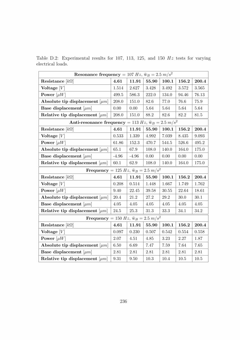
Table D.2: Experimental results for 107, 113, 125, and 150 Hz tests for varyingelectrical loads.
Resonance frequency = 107 Hz, wB = 2.5 m/s2
Resistance [kΩ] 4.61 11.91 55.90 100.1 156.2 200.4
Voltage [V ] 1.514 2.627 3.428 3.492 3.572 3.565
Power [µW ] 499.5 586.3 222.0 134.0 94.46 76.13
Absolute tip displacement [µm] 208.0 151.0 82.6 77.0 76.6 75.9
Base displacement [µm] 0.00 0.00 5.64 5.64 5.64 5.64
Relative tip displacement [µm] 208.0 151.0 88.2 82.6 82.2 81.5
Anti-resonance frequency = 113 Hz, wB = 2.5 m/s2
Resistance [kΩ] 4.61 11.91 55.90 100.1 156.2 200.4
Voltage [V ] 0.533 1.339 4.992 7.039 8.435 9.093
Power [µW ] 61.86 152.3 470.7 544.5 526.6 495.2
Absolute tip displacement [µm] 65.1 67.9 108.0 140.0 164.0 175.0
Base displacement [µm] -4.96 -4.96 0.00 0.00 0.00 0.00
Relative tip displacement [µm] 60.1 62.9 108.0 140.0 164.0 175.0
Frequency = 125 Hz, wB = 2.5 m/s2
Resistance [kΩ] 4.61 11.91 55.90 100.1 156.2 200.4
Voltage [V ] 0.208 0.514 1.448 1.667 1.749 1.762
Power [µW ] 9.40 22.45 39.58 30.55 22.64 18.61
Absolute tip displacement [µm] 20.4 21.2 27.2 29.2 30.0 30.1
Base displacement [µm] 4.05 4.05 4.05 4.05 4.05 4.05
Relative tip displacement [µm] 24.5 25.3 31.3 33.3 34.1 34.2
Frequency = 150 Hz, wB = 2.5 m/s2
Resistance [kΩ] 4.61 11.91 55.90 100.1 156.2 200.4
Voltage [V ] 0.097 0.230 0.507 0.542 0.554 0.558
Power [µW ] 2.07 4.51 4.85 3.23 2.27 1.87
Absolute tip displacement [µm] 6.50 6.69 7.47 7.59 7.64 7.65
Base displacement [µm] 2.81 2.81 2.81 2.81 2.81 2.81
Relative tip displacement [µm] 9.31 9.50 10.3 10.4 10.5 10.5
236

Appendix E
Coupled Electromechanical Model:
Code
The coded implementation of the coupled electromechanical model, developed in Sec-
tion 3.3, is given below for Device 2. Device 2 is a PZT-5A-based cantilevered bi-
morph harvester which is poled for series connection operation. This code was used
for the model validation/verification in Section 5.3, specifically for predicting the de-
vice response at the specified operating points (frequencies and electrical loads). The
predicted and experimentally measured responses are compared in Figures 5-5 to 5-8.
clc;
clear all;
close all;
disp(’PiezoSystems,Inc.:T226-A4-503X’);
%%%%%%%%%%%%%%%%%%%%%%%%%%%%%%%%%%%%%%%%%%%%%%%%%%%%%%%%%%%%%%%%%%%%
% MATERIAL PROPERTIES
%%%%%%%%%%%%%%%%%%%%%%%%%%%%%%%%%%%%%%%%%%%%%%%%%%%%%%%%%%%%%%%%%%%%
% Piezo material properties
Eps_0 = 8.854e-12;
Eps_T_33 = 1800*8.854e-12;
rho_p = 7800;
d31 = -190e-12;
cE11 = 66e9;
% Calculate material properties for current configuration
% Plate configuration
% cE11 = sE11/(sE11^2-sE12^2);
237

% e31 = d31/(sE11+sE12);
% Eps_S_33 = Eps_T_33-2*d31^2/(sE11+sE12);
% KS33 = Eps_S_33/Eps_0
% Beam Configuration
% cE11 = 1/sE11;
% e31 = d31/sE11;
e31 = -14; % fit to frequency spacing
% Eps_S_33 = Eps_T_33-d31^2/sE11;
Eps_S_33 = Eps_T_33-d31*e31;
KS33 = Eps_S_33/Eps_0;
% Parameter assignment
c_E = cE11;
e_m = e31;
Eps_S = Eps_S_33;
% Material properties for layers
E_pzt_p = c_E; % PZT plate stiffness
rho_pzt = rho_p;
% structure
E_s = 100e9; % calculated
rho_s = 7165; % measured
nu_s = 0; % beam configuration
E_s_p = E_s/(1-nu_s^2); % stiffness
%%%%%%%%%%%%%%%%%%%%%%%%%%%%%%%%%%%%%%%%%%%%%%%%%%%%%%%%%%%%%%%%%%%%
% Define device parameters
%%%%%%%%%%%%%%%%%%%%%%%%%%%%%%%%%%%%%%%%%%%%%%%%%%%%%%%%%%%%%%%%%%%%
L = 55.e-3; % length in m
b = 31.8e-3; % beam width in m
% Specify layer thicknesses
t_pzt = 270e-6;
t_s = 140e-6
% Define parameters for mass at tip, not applicable for this case
L0 = 0; % length of the mass == 0 (no mass)
H0 = 70e-6; % thickness of the mass
b0 = b; % width of the mass
rho_0 = 1200; % density of mass
% mechanical damping
Zeta_m = 0.0178; % measured
ddW_b = 2.5; % input vibration amplitude
% index of pzt element above the neutral axis
ind_pzt = 3;
% Specify geometry
t_l = [t_pzt t_s t_pzt];
E_l = [E_pzt_p E_s_p E_pzt_p];
238

rho_l = [rho_pzt rho_s rho_pzt];
%%%%%%%%%%%%%%%%%%%%%%%%%%%%%%%%%%%%%%%%%%%%%%%%%%%%%%%%%%%%%%%%%%%%
% Calculate neutral axis, I, EI, rho, etc.
%%%%%%%%%%%%%%%%%%%%%%%%%%%%%%%%%%%%%%%%%%%%%%%%%%%%%%%%%%%%%%%%%%%%
% Determine the neutral axis (NA)
for ii = 1: length(t_l)
if ii == 1
zb_l(ii) = t_l(ii)/2;
else
zb_l(ii) = zb_l(ii-1) + t_l(ii-1)/2 + t_l(ii)/2;
end % if
EAzb(ii) = zb_l(ii)*t_l(ii)*b*E_l(ii);
EA(ii) = t_l(ii)*b*E_l(ii);
end % for
zb = sum(EAzb)/sum(EA);
% useful values for later calculation
zp_max = zb_l(ind_pzt)+t_pzt/2-zb; % max piezo distance from NA
zp_ave = abs(zb_l(ind_pzt)-zb); % distance: NA to piezo center
t_t = sum(t_l); % total modeled thickness
% determine the moment of inertia for each layer
for ii = 1:length(t_l)
I_l(ii) = 1/12*b*t_l(ii)^3 + t_l(ii)*b*(zb_l(ii)-zb)^2;
end % for ii
% Moment of area
I_s = sum(I_l);
% effective EI
EI_s = 0;
for ii=1:length(t_l)
EI_s = EI_s + E_l(ii)*I_l(ii);
end % for ii
% effective young’s modulus
E_eff = EI_s/I_s;
% effective density
rho_c = 0;
for ii = 1:length(t_l)
rho_c = rho_c +t_l(ii)*rho_l(ii);
end % for ii
rho_c = rho_c/t_t;
% mass per length
m = rho_c*b*t_t; % mass per length
%%%%%%%%%%%%%%%%%%%%%%%%%%%%%%%%%%%%%%%%%%%%%%%%%%%%%%%%%%%%%%%%%%%%
239

% Calculate parameters for modal analysis
%%%%%%%%%%%%%%%%%%%%%%%%%%%%%%%%%%%%%%%%%%%%%%%%%%%%%%%%%%%%%%%%%%%%
% Effect of non-point loaded proof mass
m0 = b0*(rho_c*t_t + rho_0*H0);
CG_m =(rho_c*t_t*b0*zb+rho_0*H0*b0*(t_t+H0/2))/(rho_c*t_t+rho_0*H0);
ox = L0/2; % depends on the beam config
oy = CG_m-zb; % distance from CG of mass to neutral axis
M0 = m0*L0;
M0_ = M0/(m*L);
% determine the static moment
S0 = M0*ox;
S0_ = S0/(m*L^2);
% determine the moment of inertia of the mass
for ii=1:length(t_l)
Iz(ii) = rho_l(ii)*b0*(1/12*L0*t_l(ii)^3+...
t_l(ii)*L0*(zb_l(ii)-CG_m)^2);
Ix(ii) = rho_l(ii)*b0*(1/12*t_l(ii)*L0^3);
end IzM = rho_0*b0*(1/12*L0*H0^3 + H0*L0*(t_t+H0/2-CG_m)^2);
IxM = rho_0*b0*(1/12*H0*L0^3);
Iyy = sum(Iz) + sum(Ix) + IzM + IxM;
I0 = Iyy+M0*(ox^2+oy^2);
I0_ = I0/(m*L^3);
%%%%%%%%%%%%%%%%%%%%%%%%%%%%%%%%%%%%%%%%%%%%%%%%%%%%%%%%%%%%%%%%%%%%
% Modal Analysis (for beam with non-point loaded proof mass)
%%%%%%%%%%%%%%%%%%%%%%%%%%%%%%%%%%%%%%%%%%%%%%%%%%%%%%%%%%%%%%%%%%%%
% Find the value for sigma_N*L - range and search increments
x = [1.87:0.0001:1.88]; % w/o mass
for ii=1:length(x)
A11(ii) = (sinh(x(ii))+sin(x(ii)))+I0_*x(ii)^3*(-cosh(x(ii))+...
cos(x(ii))) + S0_*x(ii)^2*(-sinh(x(ii))+sin(x(ii)));
A12(ii) = (cosh(x(ii))+cos(x(ii)))+I0_*x(ii)^3*(-sinh(x(ii))-...
sin(x(ii))) + S0_*x(ii)^2*(-cosh(x(ii))+cos(x(ii)));
A21(ii) = (cosh(x(ii))+cos(x(ii)))+M0_*x(ii)^1*( sinh(x(ii))-...
sin(x(ii))) + S0_*x(ii)^2*( cosh(x(ii))-cos(x(ii)));
A22(ii) = (sinh(x(ii))-sin(x(ii)))+M0_*x(ii)^1*( cosh(x(ii))-...
cos(x(ii))) + S0_*x(ii)^2*( sinh(x(ii))+sin(x(ii)));
% Calculate determinant of matrix
DET(ii) = A11(ii)*A22(ii)-A12(ii)*A21(ii);
end
% Find roots
if sign(DET(1)) == 1
Ind = find(DET<0);
elseif sign(DET(1)) == -1
240

Ind = find(DET>0);
end
Ind = Ind(1);
B1_L = x(Ind); % lambda_N*L
clear x;
% calculate model parameters
B1 = B1_L/L; % lambda_N for current configuration
c1 = 1; % arbitrary constant - cancels
s1 = A12(Ind)/A11(Ind);
% natural freq from modal analysis
om_n_a = B1^2*sqrt(EI_s/m);
f = om_n_a/2/pi;
%%%%%%%%%%%%%%%%%%%%%%%%%%%%%%%%%%%%%%%%%%%%%%%%%%%%%%%%%%%%%%%%%%%%
% Calculate lumped element model parameters
%%%%%%%%%%%%%%%%%%%%%%%%%%%%%%%%%%%%%%%%%%%%%%%%%%%%%%%%%%%%%%%%%%%%
% Solving intergrals analytically with symbolic toolbox, following
% analytical expressions are obtained and solved for each case. Note
% these functions have been truncated!
xa = 0;
xb = L;
Int_Phi_2 = -1/8*c1^2*(-exp(-2*xb*B1)*s1^2*exp(4*xb*B1)+(truncated)
Int_ddPhi_2 = 1/8*c1^2*B1^3*exp(-2*xa*B1)+1/2*c1^2*B1^3*(truncated)
Int_Phi = c1*(sinh(xb*B1)-sin(xb*B1)-s1*cosh(xb*B1)-(truncated)
Int_ddPhi= c1*B1*sinh(xb*B1)+c1*B1*sin(xb*B1)-c1*B1*s1*(truncated)
clear xa xb;
% Mode shape value calculations
Phi_L = c1*((cosh(B1*L)-cos(B1*L))-s1*(sinh(B1*L)-sin(B1*L)));
dPhi_L = c1*B1*((sinh(B1*L)+sin(B1*L))-s1*(cosh(B1*L)-cos(B1*L)));
ddPhi_0 =c1*B1^2*((cosh(B1*0)+cos(B1*0))-s1*(sinh(B1*0)+sin(B1*0)));
% calculate coefficient matrices
% Mass matrix
for ii = 1:length(t_l)
M_l(ii) = b*t_l(ii)*rho_l(ii)*Int_Phi_2;
end % for ii
M1 = sum(M_l) + M0*Phi_L^2 + 2*S0*Phi_L*dPhi_L + I0*dPhi_L^2;
% Stiffness
for ii = 1:length(t_l)
K_l(ii) = E_l(ii)*I_l(ii)*Int_ddPhi_2;
end % for ii
K1 = sum(K_l);
241

% Coupling matrix
Theta = b*zp_ave*e_m*dPhi_L; % for a single element
Theta = Theta; % effective coupling for series connection
% Capacitance
Cp = b*L*Eps_S/t_pzt; % For a single element
Cp = Cp/2; % effective capacitance for series connection
% System coupling, kappa
Ke_2 = Theta^2/(K1*Cp);
% Input matrix
Bf = m*Int_Tsi + M0*Phi_L + 1/2*M0*dPhi_L*(2*L+L0);
% estimate the natural frequency acc to lumped model
om_n = sqrt(K1/M1); % check to compare against modal analysis
%%%%%%%%%%%%%%%%%%%%%%%%%%%%%%%%%%%%%%%%%%%%%%%%%%%%%%%%%%%%%%%%%%%%
% Specify frequencies and loads at which system response is analyzed
%%%%%%%%%%%%%%%%%%%%%%%%%%%%%%%%%%%%%%%%%%%%%%%%%%%%%%%%%%%%%%%%%%%%
om = [70*2*pi 95*2*pi om_n om_n*sqrt(1+Ke_2) 125*2*pi 150*2*pi]’;
OM = om/om_n; % normalize
Rl = [4.61 11.91 19.90 55.9 100.1 156.2 200.4].*1000;
Re = Rl*Cp*om_n; % dimensionless time constant, alpha
%%%%%%%%%%%%%%%%%%%%%%%%%%%%%%%%%%%%%%%%%%%%%%%%%%%%%%%%%%%%%%%%%%%%
% Calculate system response at these loads and frequencies
%%%%%%%%%%%%%%%%%%%%%%%%%%%%%%%%%%%%%%%%%%%%%%%%%%%%%%%%%%%%%%%%%%%%
% Calculate optimal resistances at OC and SC
OM_oc = sqrt(1+Ke_2); % Anti-resonance frequency
r_opt = (OM_oc^4 + (4*Zeta_m^2-2)*OM_oc^2 + 1)/(OM_oc^6 + ...
(4*Zeta_m^2-2*(1+Ke_2))*OM_oc^4+(1+Ke_2)^2*OM_oc^2);
Re_opt_oc = sqrt(r_opt);
Rl_opt_oc = round(Re_opt_oc/(Cp*om_n));
OM_sc = 1; % Resonance frequency
r_opt = (OM_sc^4 + (4*Zeta_m^2-2)*OM_sc^2 + 1)/(OM_sc^6 + ...
(4*Zeta_m^2-2*(1+Ke_2))*OM_sc^4 + (1+Ke_2)^2*OM_sc^2);
Re_opt_sc = sqrt(r_opt);
Rl_opt_sc = round(Re_opt_sc/(Cp*om_n));
Rl_opt_df = Rl_opt_oc-Rl_opt_sc;
% Calculate the optimum frequency ratio for a given electrical load
factor_H = 4*Zeta_m^2 - 2*(1+Theta^2/(K1*Cp));
% calculate optimum frequency numerically
for ii=1:length(Re)
OM_opt_roots = roots([2*Re(ii)^2 (1+factor_H*Re(ii)^2) 0 -1]);
for jj=1:length(OM_opt_roots)
242

if real(OM_opt_roots(jj))>0
OM_opt(ii) = sqrt(OM_opt_roots(jj));
end
end
end
% Use coefficients to calculate the response of the system
for ii=1:length(Re)
for jj=1:length(OM)
den = sqrt((1-(1+2*Zeta_m*Re(ii))*OM(jj)^2)^2+((2*Zeta_m...
+(1+Theta^2/(K1*Cp))*Re(ii))*OM(jj)-Re(ii)*OM(jj)^3)^2);
Z(ii,jj) = (Bf/K1*sqrt(1+Re(ii)^2*OM(jj)^2))*ddW_b/den;
W_tip(ii,jj) = Phi_L*Z(ii,jj);
Rot_tip(ii,jj) = dPhi_L*Z(ii,jj);
Str_m(ii,jj)= -zp_max*ddPhi_0*Z(ii,jj);
Vp(ii,jj) = Bf*Re(ii)*Ke_2*OM(jj))*ddW_b/abs(Theta)/den;
Pout(ii,jj) = om_n/K1*Re(ii)*Ke_2*OM(jj)^2 / den^2;
Ip(ii,jj) = Pout(ii,jj)/Vp(ii,jj);
end
end
% Calculate response for power-optimal resistance at each frequency
for ii=1:length(OM)
Re_opt_f(ii)=sqrt((OM(ii)^4+(4*Zeta_m^2-2)*OM(ii)^2+1)/(OM...
(ii)^6+(4*Zeta_m^2-2*(1+Ke_2))*OM(ii)^4+(1+Ke_2)^2*OM(ii)^2));
Rl_opt_f(ii) = Re_opt_f(ii)/(Cp*om_n);
den_opt=sqrt((1-(1+2*Zeta_m*Re_opt_f(ii))*OM(ii)^2)^2+...
((2*Zeta_m+(1+Theta^2/(K1*Cp))*Re_opt_f(ii))*OM(ii)-...
Re_opt_f(ii)*OM(ii)^3)^2);
Z_opt(ii)= Bf/K1*sqrt(1+(Re_opt_f(ii)*OM(ii))^2)*ddW_b/den_opt;
W_tip_opt(ii) = Phi_L*Z_opt(ii);
Rot_tip_opt(ii) = dPhi_L*Z_opt(ii);
Str_m_opt(ii) = -zp_max*ddPhi_0*Z_opt(ii);
Vp_opt(ii) = Bf*Re_opt_f(ii)*Ke_2*OM(jj))*ddW_b/abs(Theta)/den;
Pout_opt(ii)= om_n/K1*Re_opt_f(ii)*Ke_2*OM(jj)^2 / den^2;
I_opt(ii) = Pout_opt(ii)/Vp_opt(ii);
end
% calculate mechanical response across length of structure
x_a = [0:L/100:L]’;
for ii=1:length(x_a)
den = sqrt((1-(1+2*Zeta_m*Re_opt_sc)*OM_sc^2)^2+((2*Zeta_m+...
(1+Ke_2)*Re_opt_sc)*OM_sc-Re_opt_sc*OM_sc^3)^2);
Z_1(ii) = Bf/K1*sqrt(1+(Re_opt_sc*OM_sc)^2)*ddW_b / den
W_1(ii) = c1*((cosh(B1*x_a(ii))-cos(B1*x_a(ii)))-...
243

s1*(sinh(B1*x_a(ii))-sin(B1*x_a(ii))))*Z_1(ii);
Str_1(ii) = -zp_max*(c1*B1^2*((cosh(B1*x_a(ii))+cos(B1*x_a...
(ii)))-s1*(sinh(B1*x_a(ii))+sin(B1*xv(ii)))))*Z_1(ii);
end
% calculate device power density
% operating volume
volume = (2*max(abs(W_tip_opt))+H0*cos(max(abs(Rot_tip_opt)))+...
L0*sin(max(abs(Rot_tip_opt))))*(L+L0)*(max(b,b0))*1e6;
P_dens = (max(Pout_opt(:))/1e-6)/volume;
244