physical-layer modeling and system-level design of …luca/research/pnocs_tcad11.pdf · ieee...
TRANSCRIPT

IEEE TRANSACTIONS ON COMPUTER-AIDED DESIGN OF INTEGRATED CIRCUITS AND SYSTEMS, VOL. 30, NO. 10, OCTOBER 2011 1507
Physical-Layer Modeling and System-Level Designof Chip-Scale Photonic Interconnection Networks
Johnnie Chan, Student Member, IEEE, Gilbert Hendry, Student Member, IEEE, Keren Bergman, Fellow, IEEE,and Luca P. Carloni, Senior Member, IEEE
Abstract—Photonic technology is becoming an increasinglyattractive solution to the problems facing today’s electronicchip-scale interconnection networks. Recent progress in siliconphotonics research has enabled the demonstration of all thenecessary optical building blocks for creating extremely high-bandwidth density and energy-efficient links for on-chip andoff-chip communications. From the feasibility and architectureperspective however, photonics represents a dramatic paradigmshift from traditional electronic network designs due tofundamental differences in how electronics and photonicsfunction and behave. As a result of these differences, newmodeling and analysis methods must be employed in order toproperly realize a functional photonic chip-scale interconnectdesign. In this paper, we present a methodology for characterizingand modeling fundamental photonic building blocks whichcan subsequently be combined to form full photonic networkarchitectures. We also describe a set of tools which can beutilized to assess the physical-layer and system-level performanceproperties of a photonic network. The models and toolsare integrated in a novel open-source design and simulationenvironment. We present a case study of two differentphotonic networks-on-chip to demonstrate how our improvedunderstanding and modeling of the physical-layer details ofphotonic communications can be used to better understand thesystem-level performance impact.
Index Terms—Optical communications, optical crosstalk,optical losses, photonic interconnection networks, simulationsoftware, system analysis and design.
Manuscript received August 21, 2010; revised January 24, 2011; acceptedApril 21, 2011. Date of current version September 21, 2011. This researchis supported in part by the Defense Advanced Research Projects Agency(DARPA) Microsystems Technology Office, under Grant ARL-W911NF-08-1-0127, the National Science Foundation, under Award 0811012, andthe Interconnect Focus Center, one of the five research centers fundedunder the Focus Center Research Program by the Semiconductor ResearchCorporation and DARPA Program. The views, opinions, and findingscontained in this paper are those of the authors and should not beinterpreted as representing the official views or policies, either expressedor implied, of the Defense Advanced Research Projects Agency or theDepartment of Defense. An earlier version of this paper was presented atthe 2010 Design, Automation Test in Europe Conference (DATE), Dresden,Germany, March 2010. This paper was recommended by Associate EditorR. Marculescu.
J. Chan, G. Hendry, and K. Bergman are with the Department ofElectrical Engineering, Columbia University, New York, NY 10027 USA(e-mail: [email protected]; [email protected]; [email protected]).
L. P. Carloni is with the Department of Computer Science, ColumbiaUniversity, New York, NY 10027 USA (e-mail: [email protected]).
Color versions of one or more of the figures in this paper are availableonline at http://ieeexplore.ieee.org.
Digital Object Identifier 10.1109/TCAD.2011.2157157
I. Introduction
THE COMPUTING industry has been steadily increasingthe number of cores on a single processor die to raise
performance through parallel computation. In order for chipmultiprocessor (CMP) systems to properly function and takeadvantage of the multiple cores, interconnection networksare required to provide both on-chip (e.g., core to core)and off-chip (e.g., core to main memory) communicationlinks. Electronic interconnection networks have thus far beencapable of coping with the communication demands oftoday’s applications, however further scaling of the numberof cores and memory requirements of applications maynot be able to be matched with equivalent communicationimprovements [1]. This inability of electronic interconnectsto scale in performance is a consequence of the largeamount of power that is dissipated by the electronicinterconnects and the limited heat-dissipation capabilities ofcurrent packaging technology. A previous study has shownthat over 50% of the dynamic power dissipated in some high-performance microprocessors comes from the interconnectsexclusively [2]. These problems will be further exacerbatedas the requirements of CMP systems continue to grow,exemplifying the need for a new interconnect technology thatcan deliver energy-efficient high-bandwidth communications.
Photonics technology has emerged as a promising chip-scale interconnect solution to the various challenges facingCMP scaling. Photonic signaling using wavelength divisionmultiplexing (WDM) can enable orders of magnitude higherbandwidth density than electronics which is becomingincreasingly constrained by the wire and pin densities thatcan be achieved [1]. The power dissipation of photonicsignaling can be designed to be practically independent ofdistance and data rate. This allows for high-speed data toflow seamlessly between the on-chip and off-chip domains.All the necessary optical devices for creating chip-scalephotonic interconnection networks have been demonstratedusing complementary metal-oxide-semiconductor (CMOS)-compatible fabrication techniques, as described in Section IV.This compatibility allows them to be economically producedin existing fabrication lines. Moreover, CMOS compatibilityallows these optical devices to be directly integrated withelectronic digital circuits, providing a flexible and powerfulmeans to create a high-performance interconnect fabric.
In light of these recognized advantages of optics, manychallenges still exist in fathoming and creating a chip-scale
0278-0070/$26.00 c© 2011 IEEE

1508 IEEE TRANSACTIONS ON COMPUTER-AIDED DESIGN OF INTEGRATED CIRCUITS AND SYSTEMS, VOL. 30, NO. 10, OCTOBER 2011
photonic network. Chip-scale silicon photonics currentlyprovides no means of in-flight buffering and logicalprocessing. The only way to accomplish these tasks isto use optical-electronic-optical (O-E-O) conversion, anddo them in the electronic domain. O-E-O conversion istolerated in switches for large-scale networks, howeverthe additional power dissipation required would have adetrimental impact on chip-scale systems. Signal regenerationis also not easily accomplished in the CMOS-compatiblephotonic platform, therefore network architecture designsmust carefully consider the optical losses to ensure signalintegrity throughout the transmission path. Conventionalnetwork simulators are not well suited for photonic networkssince they are incapable of capturing all the physical andfunctional details that differentiate photonic devices fromtheir electronic counterparts.
In this paper, we present a methodology for designing,modeling, and analyzing the performance of photonicinterconnection networks. Furthermore, this paper highlightsseveral techniques to synergistically study a photonicarchitecture’s system-level properties through physical-layeranalysis. We have also developed the PhoenixSim environmentwhich integrates the modeling and analysis aspects of ourmethodology and has been made publicly available [3].PhoenixSim is implemented using OMNeT++, a C++-basedevent-driven simulation environment [4]. Our methodologyand PhoenixSim represent a novel set of tools which systemarchitects can use to see how integrated photonics canpotentially impact the performance of a particular computingsystem.
In Section II, we review related work in the area of photonicnetwork architectures and other simulators and tools that havebeen developed to model and design them. In Section III, wepresent our methodology and outline the design flow supportedby PhoenixSim which guides designers from the modeling ofthe basic silicon photonics devices, through the compositionof the devices into a complex interconnection network, tothe analysis of the network performance and scalability. InSection IV, we describe our method for modeling photonicdevices and overview a library of fundamental buildingblocks we have implemented. In Section V, we presenta unique set of analysis tools for optimizing photonicinterconnection networks. We then discuss two photonicnetwork-on-chip architectures as case studies in Section VIto demonstrate how our methodology can be used to designand understand photonic interconnection networks. We finishwith our concluding remarks in Section VII.
This paper expands upon work that has been publishedpreviously [5]. New contributions include: 1) a completediscussion of our proposed design methodology; 2) themodeling of Mach-Zehnder switches in our Photonic DeviceLibrary; 3) the expansion of our noise model to handleintra-message crosstalk and receiver noise; and 4) inclusionof serialization/de-serialization (SerDes) power within ourpower model. We also conduct our case study on newnetwork topologies and include a more extensive set ofresults and analysis. Lastly, we include an expanded literaturereview of photonic interconnection network architectures
and photonic interconnect computer-aided design (CAD)tools.
II. Related Work
A. Photonic Interconnection Networks
Many photonic interconnect architectures have beenproposed in recent years for improving the performance andefficiency of computing systems. Photonics offers an entirelynew design space to explore and optimize, potentially causingparadigm shifts in a variety of architectural issues suchas memory hierarchies, programming models, and physicallayouts. Many topologies have been proposed by the researchcommunity, consisting of designs that leverage wavelength-,spatial-, and time-based routing. Below, we review a sampleof the various proposed topologies.
The Corona network is a proposed network that integratesphotonic interconnects for use in both on-chip and off-chipcommunications [6]. The on-chip network is implemented witha serpentine crossbar and arbitration is handled with an opticaltoken-ring based scheme and transmission is conducted usingwavelength routing. Each memory controller can interface willmultiple memory modules to create a memory solution withscalable capacity.
Joshi et al. proposed a mapping of the Clos topologyfor use as an on-chip photonic network [7]. This proposednetwork architecture connects a 64-core CMP through aglobal photonic crossbar. The network is source routedand arbitration is accomplished through the selection of anoptical transmission wavelength and transmission waveguidefrom a wide optical bus. Center stages of the Clos areperformed electronically, resulting in an O-E-O conversion.Other networks have also been proposed that use similarwavelength-routing scheme for arbitration [8], [9].
Batten et al. proposed an off-chip photonic interconnectionnetwork for connecting each core of a CMP to multiplememory banks [10]. The topology uses a crossbar matrix,implemented using ring filters for wavelength-based routing,to fully connect each on-chip computing node to all memorybanks. The network is nonblocking and only requires asimple source-routing scheme for transmission. The Phastlanetopology is another dedicated photonic network used forhandling cache-coherency of a shared-memory CMP [11].
A circuit-switching style network was originally proposedby Shacham et al. that uses active switching for the spatialrouting of photonic messages [12]. The network dedicatesthe entire optical spectrum for data parallelism to createhigh-bandwidth links using WDM, which contrasts with theaforementioned topologies that leverage the spectrum forrouting purposes. Further studies of this routing scheme havealso been conducted for varying topologies [13], [14] andapplications [15].
Hendry et al. [16] proposed time-division multiplexing(TDM) as an alternative to circuit-switching to eliminate thelatency overhead of the path-setup protocol. TDM routing isenabled by temporally dividing the transmission medium intoa constant series of frames. Multiple time slots compose eachframe and a unique network configuration consisting of some

CHAN et al.: PHYSICAL-LAYER MODELING AND SYSTEM-LEVEL DESIGN OF CHIP-SCALE PHOTONIC INTERCONNECTION NETWORKS 1509
Fig. 1. Design flow of modeling a network in the PhoenixSim environment.
network connectivity is assigned to each time slot. The set ofall time slots within a frame will contain a set of connectionsthat completely connect all nodes within the network.
B. CAD Tools
As the interest for using photonic interconnects continues togrow, so does the need for tools that can harness the potentialof this new technology. In the realm of simulation, two levelsexist which are of interest to photonic network designers: link-level and system-level. Simulation is an especially importantpredictive tool for gauging the performance of these photonicinterconnect systems which are too complex for manufacturingin current fabrication technology. Beyond simulation, designtools will be needed to effectively and accurately designcomplex and efficient photonic interconnection networks. Mostconventional simulation and design tools are not ideally suitedfor capturing the physical and performance characteristicsof chip-scale photonic interconnection devices and networks.Therefore the development of photonically enabled tools isneeded to fill the void.
As photonic interconnect topologies are becomingincreasingly complex, layout tools and optimization techniqueswill be required for efficient and accurate design. Dinget al. have developed Optical Interconnect Library (OIL) asynthesis-like CAD tool for optimizing optical router designsin terms of insertion loss [17]. The methodology allows forconstraint based optimization in terms of latency and insertionloss. Similarly, Minz et al. have devised a synthesis tool fortiming-driven optimization of optical waveguide placementin an on-chip network [18]. VANDAL is a place-and-routetool for on-chip photonic architectures which uses a libraryof modeled and characterized components, and includesautomation tools for rapid design and synthesis [19].
With link-level simulation, the primary concern is detailedphysical modeling of all the end-to-end aspects of a photonicpath to determine performance metrics such as signal integrityand link reliability. O’Connor et al. [20] proposed a link-level simulation environment for heterogeneous photonicintegrated circuits which leverages detailed synthesizablemodels of building-block components for the purpose ofdetermining interconnect density, area, link delay, and linkpower requirements. Similarly, De Wilde et al. [21] presentedan approach for characterizing CMOS-to-CMOS links in terms
of timing, error rates, and noise sensitivity. The IBM opticallink simulator was created to design and analyze telecom-scale and LAN-scale links through metrics such as failurerates, power penalties, and signal performance (e.g., eyediagrams) [22].
System-level simulation uses a higher-level of abstractionthan link-level simulation and is primarily concerned withdetermining network performance metrics (e.g., bandwidth,application latency, and system power dissipation). Briereet al. [23] have developed the ONoC SystemC model whichfocuses on the simulation of optical networks-on-chip usingthe SystemC framework and primarily addressing high-levelsystem concerns including device timing and network-levelpower dissipation. Their modeling is currently specific totopologies that leverage the lambda router, which routesoptical traffic based on the wavelength of light that is beingused by the source. Optisim is a system-level simulator formodeling optical interconnects in board-based and cluster-based computing [24].
PhoenixSim is primarily categorized as a system-levelsimulation environment that includes some aspects oflink-level simulation. Our PhoenixSim environment closelyresembles Optisim with respect to the use of a photonicbuilding block library, and extractability of physical andsystem metrics. We differentiate our work from Optisimthrough combination of our focus on chip-scale systems,support for spatial and temporal based photonic chip-scalearchitectures, and synergistic study of physical-layer andsystem-level performance metrics.
III. Methodology and Design Flow Overview
An overview of our design methodology is illustrated inFig. 1. The sequence of design stages we employ for modelingphotonic interconnection networks primarily consists of sixdesign steps: 1) specification of the network building blocks;2) specification of the target application; 3) modeling of thenetwork architecture; 4) system-level performance analysis;5) physical-layer characterization; and 6) iterative refinementof parameters and design.
Step 1 (as labeled in Fig. 1) involves the specification ofthe fundamental network building blocks that will be usedfor creating the interconnection network. The collection of

1510 IEEE TRANSACTIONS ON COMPUTER-AIDED DESIGN OF INTEGRATED CIRCUITS AND SYSTEMS, VOL. 30, NO. 10, OCTOBER 2011
Fig. 2. Subset of the photonic devices in the Interconnect Building BlockLibrary.
network building blocks is named the Interconnect BuildingBlock Library. Within this library is a set of photonic devicesthat are characterized using the Basic Element Device Model(Fig. 2), described in further detail in Section IV. Users ofthis design methodology can choose to design a networkbased on the included library of devices, or extend the librarythemselves with other novel photonic building blocks.
The library for electronic building blocks consists of switch,arbitrator, and buffer blocks for creating standard pipelinedrouters. PhoenixSim leverages the Orion simulator [25] forderiving detailed values for electronic delay and energydissipation. The electronic router model is highly configurableand includes parameters for clock rate, buffer size, channelwidth, and number of virtual channels. In addition to thestandard router design, the electronic router model alsoincludes additional methods for interfacing with photonicdevices. Electro-optic photonic devices can take an electronicinput to influence its optical behavior and are essentialcomponents for enabling the active types of switching usedin some proposed networks [6], [12].
Next, Step 2 consists of specifying the target application.PhoenixSim currently supports the use of both syntheticallygenerated traffic patterns and communication traces,with eventual plans for integration with a cycle-accuratemicroarchitecture simulator. A variety of syntheticpatterns have already been created within the environment(e.g., random, hotspot, nearest neighbor, and tornado) and isextensible to others. Communication traces can be generatedby monitoring the network traffic during the execution ofa real application and used as an input into PhoenixSim.Performance results gained by using communication tracesare useful in assessing the application-specific performancegains of photonic networks [15].
The design and modeling of the network occurs in Step 3of the design flow. The devices from the InterconnectBuilding Block Library can be combined to create higher-ordernetworking components and entire interconnection networktopologies. By accounting for the target applications, anetwork architect can optimize the topology design to targetspecific requirements such as message size, latency, and/orthroughput. For instance, Fig. 3 illustrates how a 4 × 4nonblocking switch can be derived within PhoenixSim byconnecting various devices from the Building Block Library.
Step 4 involves the characterization of the networkarchitecture at the physical layer, which involves metricssuch as the optical power budget, crosstalk, and powerdissipation. The overall physical-layer performance of a
Fig. 3. (a) Schematic of a design for a 4×4 nonblocking photonic switch.(b) Screenshot of how PhoenixSim composes the switch by instancing basicphotonic devices.
derived photonic component or topology can be determinedfrom the aggregate performance of the individual photonicdevices. Although this is not as rigorous as a true link-level simulator, this hierarchical building process enablesan accurate first-order physical characterization of an entirenetwork through the characterization of a small number offoundational components.
Step 5 measures the system-level performance characteri-stics of the network architecture in terms of data throughputand latency. Many of the physical properties that are identifiedin Step 4 have an impact on network functionality andscalability and play a crucial role in determining overallsystem performance.
Finally, Step 6 forms the basis for an iterative process,where the performance results and analysis of the modelednetwork can be used to refine the topology design anddevice parameters to further optimize the overall performance.Previous work has demonstrated the effectiveness of thisiterative step. The initial physical-layer characterizationsshowed the dramatic impact that waveguide crossing loss hadon performance and a subsequent analysis of a system withimproved crossings resulted in a dramatic improvement inoverall performance [14].
IV. Photonic Device Library
Our method for modeling photonic devices is designedto enable the assessment of the physical-layer performanceat a first-order approximation while concurrently allowingfor system-level analysis with a reasonable computationalrequirement. Many simulation packages use techniques suchas finite-difference time-domain (FDTD) to accurately modelan electromagnetic field according to Maxwell’s equations.FDTD analysis, however, is usually limited to a single orsmall set of devices since it is computationally intensiveand can have a large memory requirement. We use amore efficient level of abstraction by establishing a set ofcharacteristic device parameters that are key to measuringthe physical and system metrics which are important toour understanding of photonic interconnection networks. Thissimplified model enables PhoenixSim simulations to run onconventional computers in a period of minutes or hours.The device characteristics can be determined experimentally,through simulation, or projected. This set of modeled devices

CHAN et al.: PHYSICAL-LAYER MODELING AND SYSTEM-LEVEL DESIGN OF CHIP-SCALE PHOTONIC INTERCONNECTION NETWORKS 1511
Fig. 4. Parameters for characterizing a photonic device using the BasicElement Model.
composes the Photonic Device Library. While the descriptionsincluded in this paper mostly highlight silicon ring-basedtopologies, the modeling methodology can easily be used todescribe devices based on other technology domains suchas Mach-Zehnders (also described in this section), photoniccrystals, and MEMS.
The parameters used to describe basic photonic devices,called Basic Elements, are shown in Fig. 4. We refer tooptical inputs and outputs as ports. Each port is physicallybi-directional, therefore ports from which an optical signalcan ingress into can also be used to egress from, andvice versa. Certain network topologies may still require uni-directional operation of the ports to facilitate simplicity orsatisfy some other design requirement. Nonetheless, the bi-directional nature of each port is still represented for accuracy.The ports of the device are enumerated 0. . .N − 1 where N isthe number of ports of a photonic device. N also determinesthe size of additional parameter matrices used in defining thephotonic device behavior and characteristics.
We use a logical routing table to determine the path amessage takes through the device. Fig. 4 shows how therouting table can be represented as a length-N vector, wherethe index represents the ingression port of an optical signaland the value at the index represents the egression port.
Additionally, we use two tables to represent the latencyand the optical insertion loss properties of the device. Eachproperty is represented as a N×N matrix where the rowcorresponds to the port through which the optical signalingresses from (input) and the column represents the port fromwhich the optical signal egresses from (output). Each entryin a matrix corresponds to the value used for the particularinput/output combination. The latency for a particular input-output port combination is measured as the time between whenoptical signal enters the input port and when the same opticalsignal exits the output port. The insertion loss is a measureof the optical power attenuation an optical signal receiveswhen traveling through a device and is useful in characterizingnetwork-level insertion loss and crosstalk.
A. Static Elements
The Basic Element Model is most suitable for describingstatic optical devices that have characteristics that do not
change at runtime. The current library of devices focus on 2-Dplanar devices that are capable of being fabricated in a CMOS-compatible process. These static devices include waveguides,waveguide bends, waveguide crossings, and couplers.
1) Waveguides: Waveguides act as the optical wires usedto link all the various devices, sources, and destinations.Optical signals that travel along a waveguide exhibitinsertion loss in the form of propagation loss which is theattenuation experienced from traveling through the waveguide.Propagation loss is affected by a variety of parametersincluding waveguide dimensions, fabrication technique, andmaterial properties. Waveguides are modeled as 2-port deviceswith parameters for length, group velocity per unit length, andinsertion loss per unit length.
A waveguide’s routing table is [1, 0]; which indicates thatan optical signal ingressing on either end will egress on theopposite side. For a waveguide of length Lwg and propagationdelay twg, the latency matrix will be
Latencywg =
[ − Lwgtwg
Lwgtwg −]
. (1)
Note that the elements along the diagonal represent thelatency of a reflection. Since reflections are nonexistent inwaveguides, the elements of the matrix that represent thelatency of the reflection are marked as do not-care values.Similarly, the same waveguide with propagation loss of αwg
will have a insertion loss matrix of
Losswg =
[ ∞ Lwgαwg
Lwgαwg ∞]
. (2)
While reflections do not occur in the waveguide, it isuseful to assign infinite insertion loss to the reflection pathfor crosstalk calculation purposes.
The production of low-loss on-chip waveguides forthe CMOS platform is an important goal in realizingintegrated photonic networks. Silicon waveguides with crosssectional areas of approximately 500 nm × 250 nm have beendemonstrated with a 1–2-dB/cm insertion loss using [26], [27].Lower losses can be achieved using more exotic fabricationtechniques such as with etchless silicon waveguides that havebeen shown to have losses of 0.3 dB/cm [28]. The freedomof parameter specification also enables the investigation ofwaveguides composed of nonsilicon materials such as silicafiber (losses on the order of tenths of a dB per kilometer) andsilicon-nitride (losses of 0.1 dB/cm, [29]).
2) Waveguide Bends: Bends in waveguides are required toproperly direct all the optical paths in the creation of switchesand topologies. Waveguide bends contribute additionalinsertion loss to the waveguide’s existing propagation loss,which we refer to as bending loss. Bends are modeled as2-port devices and take parameters for loss per degree andangle of the bend. Silicon waveguide bending losses have beenexperimentally measured to be 0.005 dB per 90° turn with abending radius of 6.5 μm [26].
3) Waveguide Crossings: Waveguide crossings areinherently required in silicon-based on-chip topologies due tothe 2-D planar nature of the technology platform. Crossingsoccur whenever two waveguides intersect and can exhibit both

1512 IEEE TRANSACTIONS ON COMPUTER-AIDED DESIGN OF INTEGRATED CIRCUITS AND SYSTEMS, VOL. 30, NO. 10, OCTOBER 2011
Fig. 5. Organization of building block element classes within PhonixSim.
insertion loss and crosstalk which can have an impact onsystem scalability and performance. This is in distinct contrastwith electronic interconnects, which do not allow arbitrarycrossings of two wires since this would cause a short circuit.The model for crossings are configured as 4-port devices withparameters for the loss and crosstalk.
Since many topologies require a large number of waveguidecrossings, it is important for these devices to exhibit both lowinsertion loss and low crosstalk. A 6 μm × 6 μm double-etchedcrossing design has been fabricated and tested, and was shownto have fairly low insertion loss at 0.16 dB and high crosstalksuppression at about −40 dB [30].
4) Couplers: The cross-boundary interface that separatesthe on-chip and off-chip domain presents a distinct situationwhere photonics can break through performance bottlenecksthat are typically experienced by electronics. The capacitiveeffects of metal wires cause limitations in both the distanceand rate at which data can be transmitted electronically,consequently causing problems when trying to scale I/Operformance which can potentially require long wires thattravel off-chip and across a board. Instead, optical signals arepractically transparent to these issues and can be transmittedwithout penalty to extremely long distances and extremelyhigh data rates. The optical I/O interface between the on-chip and off-chip world is a coupler, which is essentiallya device for transferring light from one guiding medium toanother (e.g., from an on-chip silicon waveguide to an off-chip silica fiber). This is modeled as a 2-port device with asingle parameter for insertion loss.
There are currently two methods for implementing acoupler. Lateral coupling can be accomplished by buildinga nanotaper at the perimeter of a chip to couple into afiber and has been calculated to have theoretical losses ofunder 1 dB [31]. Vertical couplers enable the I/O interfaceto be placed on the planar surface of the chip and can beaccomplished with a Bragg grating for a ∼1-dB loss [32].The advantage of vertical coupling over lateral coupling isthe ability to position optical I/O ports anywhere on the chip.However, vertical coupling is fairly wavelength dependent dueto the selectivity of Bragg structures while lateral coupling isspectrally more broadband.
B. Ring-Resonator Elements
Ring resonators are waveguides that form a closed loopwhich can be designed to manipulate the flow of light in away that enables network functionality. Light interacts withthe rings at specific periodically spaced wavelengths in theoptical spectrum, called resonant modes. Light that enters the
Fig. 6. Propagation through a ring-resonator device depends on the signalwavelength and the resonant modes of the device. (a) Small rings with largermode spacings (shown as periodic peaks) can be designed to interact witha single wavelength channel from a WDM signal (indicated by arrows).(b) Broadband switch have tightly spaced modes, enabling many WDMchannels to couple into the device cohesively. (c) Path of propagation dependson whether the wavelength of the message is on or off-resonance with thering.
ring is said to exhibit on-resonance behavior, whereas lightthat is transparent to the ring is said to be off-resonance. Thefree spectral range (FSR) specifies the spacing of the modes,which is inversely proportional to the optical length of thering. A large-diameter ring will exhibit a small FSR (morespectrally dense), while a small-diameter ring will exhibit alarge FSR (more selective). The FSR can be manipulatedeither by altering the physical length of the ring loop orby dynamically changing the refractive index of the devicethrough electrical or thermal methods. Electrical manipulationcan be accomplished by creating a p–i–n structure on the ringwith the waveguide acting as the intrinsic region. Electricallybiasing the p–i–n structure will cause a shift in refractiveindex due to the free-carrier plasma dispersion effect insilicon [33]. This contrasts with thermal manipulation whichuses the thermo-optic properties of the material for indexchanges [34]. By using these techniques, the ring resonatorcan be engineered to perform a diverse range of networktasks [35]–[39].
To model the various ring resonator devices, we extend theBasic Element Model with subclasses for Ring Elements andDynamic Elements (Fig. 5). The Dynamic Element Model isused to describe active devices which can exhibit changes in itsrouting table, latency matrix, and loss matrix during runtime.The properties of the active device during its operationis defined by state variables which can be changed andcontrolled. The Ring Element Model supports the definitionof the resonant behavior of the devices. The behavior ofring-based devices is determined by the wavelength of theoptical signal that interacts with the component. Also shownin Fig. 5 is how Dynamic-Ring Elements can be derived fromthe individual Ring and Dynamic Element. For instance, aring-based broadband switch consists of a combination of ringresonators and electrical logic (described below) and can beelectro-optically controlled to alter the optical flow of data.
1) Filters: Optical filters are useful in selectively extractinga subset of wavelengths from a WDM message. In the limitingcase, an extremely small ring will have a large FSR andallow the filtering of a single wavelength channel. Filteringis accomplished by aligning the spectral mode of the ring

CHAN et al.: PHYSICAL-LAYER MODELING AND SYSTEM-LEVEL DESIGN OF CHIP-SCALE PHOTONIC INTERCONNECTION NETWORKS 1513
with the wavelength channel of interest [Fig. 6(a)]. Lightat wavelengths that align with the mode of the ring (onresonance) will couple from the ingression waveguide, intothe ring structure, and out onto a secondary waveguide;wavelengths of light that are not aligned (off resonance) willbe unperturbed by the ring and continue down the injectionwaveguide [Fig. 6(c)]. We model ring filter devices as single-state 4-port Ring Elements with a parameter for the ringdiameter (assuming a circle). Ring filters have been fabricatedand demonstrated on SOI with 3-μm radius, corresponding toan FSR of 30 nm [39].
2) Broadband Switches: Ring resonators are also capableof controlling the flow of an entire WDM message by aligningeach wavelength channel to a mode of the ring [Fig. 6(b)].This can be accomplished in a limited spectral range byusing a large ring with a correspondingly small FSR. Whenall the wavelength channels are on resonance, the entireWDM message will couple into the ring and onto a secondwaveguide, similar to the case of the filter. Additionally, ifthe FSR is manipulated electro-optically, all the modes canbe shifted so that the wavelength channels are no longeron resonance, thus causing the entire WDM message tonot couple into the ring. This functionality is illustratedin Fig. 6(c) for both a single-ring 1×2 photonic switchingelement (PSE) and a double-ring 2×2 PSE. These broadbandswitch elements are modeled as two-state 4-port devices. A1×2 switch composed of a ring with a 100-μm radius and 0.8-nm FSR was shown to be capable of switching 20 wavelengthchannels simultaneously [38]. Elsewhere, a fifth-order switchwas demonstrated being able to simultaneously route nine40-Gb/s wavelength channels for an aggregate data rate of360 Gb/s [37].
3) Modulators: Ring-based modulators are essentiallyhigh-speed switches. By electro-optically flipping the ringbetween an on and off-resonance state, a series of 0s and 1scan be encoded onto an optical stream of light. Light thatcouples into the ring will not egress into another waveguidelike the filters and switches, but will eventually dissipatewithin the ring. A modulator array can be formed withmultiple ring modulators so that several wavelength channelscan be encoded in parallel, creating a WDM signal (Fig. 7).Modulators should have a small ring diameter to create a largeFSR to ensure that the modulation does not interfere with otherspectrally adjacent wavelength channels. The modulator deviceis modeled as a single-state device with parameters for energydissipated per modulated bit and ring diameter. Ring-basedmodulation has been demonstrated at rates of 12.5 Gb/s in a5-μm radius silicon ring resonator [36].
4) Receivers (Photo-Detectors): Photodetectors are usedfor converting optical messages back into the electricaldomain. While the detection element itself is not a ringresonator, photo-detectors still require rings to properly filterindividual wavelength channels from an entire WDM message.Each ring filter will only allow the light from a singlewavelength channel to be incident on the photo-detectorit precedes, thereby allowing the receiver to convert asingle wavelength channel’s worth of data back into theelectrical domain. Similar to modulators, filtering should be
Fig. 7. Schematic of the conversion process between the spatially parallelelectronic domain and wavelength-parallel optical domain.
accomplished without disturbing other adjacent wavelengthchannels by using as high an FSR as possible. The detectorsensitivity determines the minimum signal power that must bereceived at the photo-detector in order for data to be properlyrecovered from the optical domain and is an importantparameter for determining the optical power budget (asdiscussed in Section V). This ring-based detection device takeparameters for energy dissipated per detected bit, sensitivity,and ring diameter. Integrated high-speed germanium detectorshave been demonstrated operating at speeds of 40 Gb/s[40], [41].
C. Mach–Zehnder Elements
Switches and modulators can also be designed using theprinciple of Mach–Zehnder interferometry (MZI). Mach–Zehnder devices are designed to operate relatively uniformlyover a large wavelength range and do not exhibit the sharpresonant peaks that ring resonators have. For instance, aMZI-based device can be used to modulate wavelengths oflight that span a large continuous wavelength range whilering-resonator modulators are limited to specific resonancewavelengths. However, this operational difference betweenMach–Zehnder devices and ring-resonator devices causesthem to not be interchangeable. The ring-based networkarchitectures analyzed in Section VI are not compatible withthese devices and would require significant changes in thedesigns. Models for 1 × 2 and 2 × 2 Mach-Zehnder switchesare currently included in the Photonic Device Library. Amodulator and switch based on MZI has been demonstratedoperating at up to 10 Gb/s [42].
V. Physical-Layer Performance Analysis
The consideration of the photonic technology domainpresents new design challenges that must be satisfied inorder to produce feasible interconnect designs. Similar toelectronics, it is important for photonic networks to considerpower dissipation and system-level performance. Furthermore,photonic networks must also consider metrics that have noelectronic equivalent such as insertion loss, the optical powerbudget, noise, and crosstalk. While a comprehensive analysisof a photonic interconnect design would involve the actualfabrication and operation of such a system, this is currentlyunrealistic since full-scale photonic on-chip networks are stillin early stages of research. Therefore, the tools presented here

1514 IEEE TRANSACTIONS ON COMPUTER-AIDED DESIGN OF INTEGRATED CIRCUITS AND SYSTEMS, VOL. 30, NO. 10, OCTOBER 2011
Fig. 8. Relationship of various parameters affecting the optical powerbudget. The difference in power of the total WDM signal (large arrow onthe left) and the individual wavelength channels (five smaller arrows on theright) constrains the scalability of the system.
can give important insight into the physical feasibility of thedesigns and the performance that is expected.
A. Optical Power Budget
The optical power budget of a photonic network assesses theamount of WDM parallelism and insertion loss that can betolerated. Many currently proposed photonic interconnectionnetworks assume off-chip lasers to provide the optical sources,which are then coupled into the chip where they are modulated,routed, and received. Optical amplification in an on-chipenvironment is not easily accomplished in the CMOS platform.For this reason, the power that is received at the photodetectorsmust remain above a certain power threshold (labeled thedetector sensitivity in Fig. 8) to ensure proper detection ofdata bit streams. This limitation can be partially compensatedfor by increasing the optical power that is injected into thechip. However, this also exhibits an upper limitation due tononlinearities of the silicon material which will potentiallydistort the signal. Distortions are caused by nonlinearitieswithin silicon which contribute additional insertion losses andcan also causes unwanted shifts in the resonances of ringresonators. This limit is labeled as nonlinear effects in Fig. 8.The difference in the two thresholds is called the optical powerbudget.
As shown in Fig. 8, the optical power budget affects thedesign choices of a given network architecture by constrainingthe sum of the WDM factor and the network insertion loss.The WDM factor measures the power difference between anentire WDM signal and its constituent wavelength channels.This factor needs to be accounted for since the nonlinearitythreshold is determined by the total power in the waveguidewhile the detector sensitivity depends on the power in theindividual wavelengths. The remaining portion of the opticalpower budget must accommodate the worst-case insertionloss that an optical message could receive in the network.Fig. 9 shows an example of the calculation involved indetermining the insertion loss for an optical signal beinginjected into a small network segment at 1 dBm. The signalis ejected at 0.24 dBm after propagating across a 0.1-cmdistance, passing by two ring resonators, and entering fourwaveguide crossings. The total loss for this example is0.76 dB. For a full-scale photonic network, all valid opticalpaths need to be examined to determine the highest-losspath.
Fig. 9. Calculation of insertion loss for a small network segment.
The relationship between the various device limitations andsystem-level metrics is summarized in the inequality
P − S ≥ ILmax + 10log10n (3)
where P is the power threshold we limit the optical power toand S is the detector sensitivity. The optical power budget isP − S. The worst-case optical path in terms of insertion lossis ILmax and n specifies the number of wavelength channelsbeing used. P , S, and ILmax are expressed in decibel units.
While it may be desirable to maximize the number ofwavelength channels used to increase bandwidth throughparallelism, and to create scalable photonic networks atthe cost of higher insertion losses, (3) shows the inherentlimitation to this. From an architectural standpoint, P and S
are fundamental design constraints imposed by the photonicdevices. Therefore, a designer must strike a balance betweenthe desired link bandwidth and the desired complexity of thenetwork. In Section VI, we illustrate the evaluation of thesetradeoffs which are made possible by PhoenixSim.
B. Data Integrity
A variety of interactions in a photonic interconnectionnetwork will work to degrade the integrity of transmitteddata. Our current noise modeling methodology accountsfor intensity noise generated at the laser sources, inter-message crosstalk, intra-message crosstalk, and electrical noisegenerated by the optical receivers (Fig. 10). The standardfigure of merit for measuring the quality of signal is the signal-to-noise ratio (SNR) which is defined as the ratio betweensignal power and noise power. From a system perspective, theSNR can be used to determine the statistical likelihood thateach bit of data is transmitted erroneously (e.g., a transmitted0 is detected as a 1), also called a bit error rate (BER). Anunderstanding of the potential noise in any interconnectionnetwork is critical to determining the effective throughput ofthe system since error detection and correction will invariablycause performance overheads.
The first source of noise is from the laser sources whichinherently cause random fluctuations in an optical signal,called intensity noise. This noise is quantified as relativeintensity noise (RIN), which is the ratio of the power varianceof the optical signal to the mean optical power squared.Quantum cascade lasers have a measured RIN on the order of−150 dB Hz−1 with an output of 10-dBm mean optical power[43]. To convert to a SNR, we use the relation [44]
SNRlaser =m2
2B · RIN(4)

CHAN et al.: PHYSICAL-LAYER MODELING AND SYSTEM-LEVEL DESIGN OF CHIP-SCALE PHOTONIC INTERCONNECTION NETWORKS 1515
Fig. 10. Sources of noise and crosstalk within a chip-scale photonic system.
where B is the noise bandwidth, assumed equal to themodulation rate, and m is the modulation index, equal to 1−E,where E is the extinction ratio of the modulator.
A second source of noise is inter-message crosstalkwhich occurs when multiple photonic messages concurrentlypropagate through a photonic device. In a waveguide crossingfor example, the ideal situation is for two orthogonallypropagating messages to be completely isolated from eachother with no interaction. However, in reality a small amountof optical power from each message will leak onto the othermessage. A similar situation occurs in ring-resonator filtersand switches due to imperfect coupling of each wavelengthchannel.
For the N-port device, the crosstalk power that a messageon a particular port receives is given by the sum of the powerthat is leaked by any existing messages on the other N − 1ports. If M is the set of all signals present in the device andthe power of a signal k is given by the variable Pk, then thecrosstalk power seen by signal s is given by∑
k∈M,k �=s
Pk
IL(portink, portouts)(5)
which aggregates the unwanted signal power that leaks intothe output port being used by s. Function IL refers to theinsertion-loss matrix (that was described in Section IV) ofthe device model with arguments for the input and outputport. In (5), portink denotes the input port of a message k,and portouts denotes the output port of s. This calculation isa first-order approximation that only considers crosstalk formessages that coexist in a device and not from leaked powerthat propagates across multiple devices before interfering witha foreign signal.
A third source of noise called intra-message crosstalkoccurs due to imperfect filtering. For example, in orderfor a WDM message to be received and converted into anelectrical signal, each wavelength channel must be individuallyfiltered and fed into a photo-detector. Due to imperfectextinction, power from the adjacent wavelength channels will
leak through causing an additional source of noise. Intra-message crosstalk will also occur in any other location ina photonic network where filtering functionality is involved.The spectral response of a ring resonator mimics a periodicLorentzian function. For simplicity we assume a periodic flatpassband and constant extinction ratio for the stop bands.Lastly, our receiver model includes thermal and shot noise.
The combined effect of these multiple sources of noise canbe used to compute an SNR for the final detected signal asfollows:
SNR =P
Nlaser + Ninter + Nintra + Ntherm + Nshot(6)
where P is the signal power and N corresponds to the noisepower associated with the noise or crosstalk source indicatedby the subscript.
C. Power Dissipation
To compute the power dissipation of the modeled networks,we add up the energy dissipation events from all devices.Our photonic device library tracks the power dissipationaccording to the type of model that is used, and caninclude both static (over a duration of time) and dynamic(instantaneous) power dissipation. Dynamic Element devicescan have static power dissipation, which is determined bythe occupied state. Dynamic Element devices can also havedynamic power dissipation, which is accumulated wheneverthere is a state transition. An additional source of powerdissipation are Ring Element devices, which require constantthermal tuning to compensate for fabrication uncertainty andambient temperature shifts. Modulator and Detector Elementsalso dissipate power during the transmission and detection ofdata, respectively.
Electronic routers are modeled as standard three-stagepipelines. The power modeling of the electronic routers isaccomplished by leveraging the Orion simulator, which iscurrently capable of modeling down to the 32 nm technologynode [25].
VI. Case Study
In this section, we model two different photonicinterconnection networks to demonstrate our methodology andthe main capabilities of PhoenixSim. The tools presented inSection V are used to quantify the performance of the networksand to demonstrate design spaces that are allotted by ourphysical-layer analysis. This case study serves to demonstratethe various capabilities of the simulator. We will show thatthe two networks offer different advantages depending on theconsidered metric and traffic pattern. Therefore this analysisserves to give system architects recommendations based ontheir design objectives.
The first photonic network we model for this case study isthe Photonic Mesh, a circuit-switching architecture originallyproposed by Shacham et al. [12] for high-bandwidth opticalcommunications on future CMPs. The network architectureconsists of a photonic network plane and an electronicnetwork plane. The electronic plane is used to transmit control

1516 IEEE TRANSACTIONS ON COMPUTER-AIDED DESIGN OF INTEGRATED CIRCUITS AND SYSTEMS, VOL. 30, NO. 10, OCTOBER 2011
Fig. 11. Photonic Mesh topology. (a) High-level representation of a 4×4Photonic Mesh. Parallel lines indicate two unidirectional waveguides, whichare paired together to form bidirectional links. Boxes represent higher-orderphotonic components, which are labeled X for 4×4 nonblocking crossbarswitch, I for injection gateway, and E for ejection gateway. Also shown aredetail schematics of the (b) 4 × 4 nonblocking crossbar switch, (c) injectiongateway, and (d) ejection gateway.
messages and provision optical resources for establishingcircuits on the photonic plane where the data messages areactually transmitted. The Photonic Mesh [Fig. 11(a)] is similarto a typical electronic mesh since it is laid out in a matrix-likeconfiguration of nodes, and has mechanisms for switching,entering the network, and exiting the network at each node.Although the mesh-based design presented here exhibitslower path diversity than previously proposed circuit-switchingtopologies [13], [14], the simpler architecture is beneficial tooverall performance by lowering total insertion loss.
A 4 × 4 nonblocking crossbar switch [Fig. 11(b)] is foundat each node of the network and is optimized for dimension-ordered routing (which is the case for the Photonic Mesh)by minimizing insertion losses along propagation paths thatdo not turn through the switch [45]. The injection gateway[Fig. 11(c)] and ejection gateway [Fig. 11(d)] designs, whichare used by the underlying processing cores to transmit andreceive optical data, are adapted from the TorusNX topologyto help further reduce insertion loss overhead caused by morecomplex injection/ejection schemes [14]. Each switch andgateway is constructed using the devices previously describedin Section IV.
The second photonic network we model for this casestudy is the Photonic Crossbar (Fig. 12). This design usesthe crossbar concepts used previously in the Photonic Clostopology [7]. A set of waveguides are routed in a serpentinemanner so that they intersect with all gateways in the network.Each individual waveguide is configured with two modulatorbanks and two receiver banks to connect a unique pair ofgateways. For a topology with G gateways, a set of G · (G −1)/2 waveguides is required to fully connect the network.Since the required number of waveguides grows quadratically
Fig. 12. Photonic Crossbar topology. (a) High-level representation of a 2×4Photonic Crossbar, connecting 16 cores. Boxes represent gateways with aconcentration of two processing cores. (b) Detail schematic of the PhotonicCrossbar gateway, showing 49 bypass waveguides and seven waveguideswith modulator and receiver banks used to communicate to the other sevengateways.
with G, it can be advantageous to concentrate the traffic ofa set of processing cores through a single photonic gateway.Each gateway exploits the bidirectionality of the waveguidesand avoids receiving its own modulated signal by transmittingand receiving on different sets of wavelengths.
Fig. 12(a) shows an 8-gateway network with two processingcores connected to each gateway. The gateway design isillustrated in Fig. 12(b). The gateway contains 49 bypasswaveguides which are ignored, and is connected to theremaining seven waveguides through a set of seven modulatorbanks and seven receiver banks. Each connected waveguidewill transmit to and receive from one of the other sevengateways in the network. Attached to each photonic gatewayis a 9-port electronic router which must transport messagesto and from the group of cores to the appropriate photonictransmitter or receiver bank.
A. Optical Power Budget Analysis
First, we used PhoenixSim to model both photonictopologies and analyze the worst-case insertion loss fornetwork radixes from 2×2 (four nodes) to 10×10 (100 nodes).The insertion loss parameters used in this paper are derivedfrom experimentally demonstrated results and are listed inTable I. Fig. 13 shows the maximum total loss exhibited withineach network and the breakdown according to type of loss. Allnetwork sizes assumed total chip dimensions of 2 cm × 2 cmand the size of the network is designed to span the entirechip. Hence the spacing between nodes will decrease withlarger radixes. Crossing loss and propagation loss are the mostsignificant contributors to total loss in the Photonic Mesh andPhotonic Crossbar, respectively. The 10 × 10 Photonic Meshhas 18.1 dB of crossing loss caused by the existence of anetwork path with 113 waveguide crossings, accounting for
CHAN et al.: PHYSICAL-LAYER MODELING AND SYSTEM-LEVEL DESIGN OF CHIP-SCALE PHOTONIC INTERCONNECTION NETWORKS 1517
TABLE I
Insertion Loss Parameters
Parameter Value ReferencePropagation loss (silicon) 1.7 dB/cm [26]Waveguide crossing 0.16 dB [30]Waveguide bend 0.005 dB/90° [26]Drop into a ring 0.6 dB [38]Pass by a ring 0.005 dB [38]
Fig. 13. Insertion loss results for the (a) Photonic Mesh and (b) PhotonicCrossbar of varying sizes. Labeled values that overlay the columns indicatethe worst-case total network-level loss values. Columns illustrate the worst-case loss associated with the individually labeled loss component which doesnot necessarily occur in the network path with the worst total loss.
approximately 63% of the total network-level insertion loss.The serpentine waveguide design of the Photonic Crossbarcauses repeated traversals of the chip, therefore causing highpropagation loss. This analysis is an important indicator fordevice researchers who may seek to focus on improving theperformance of a specific type of network architecture.
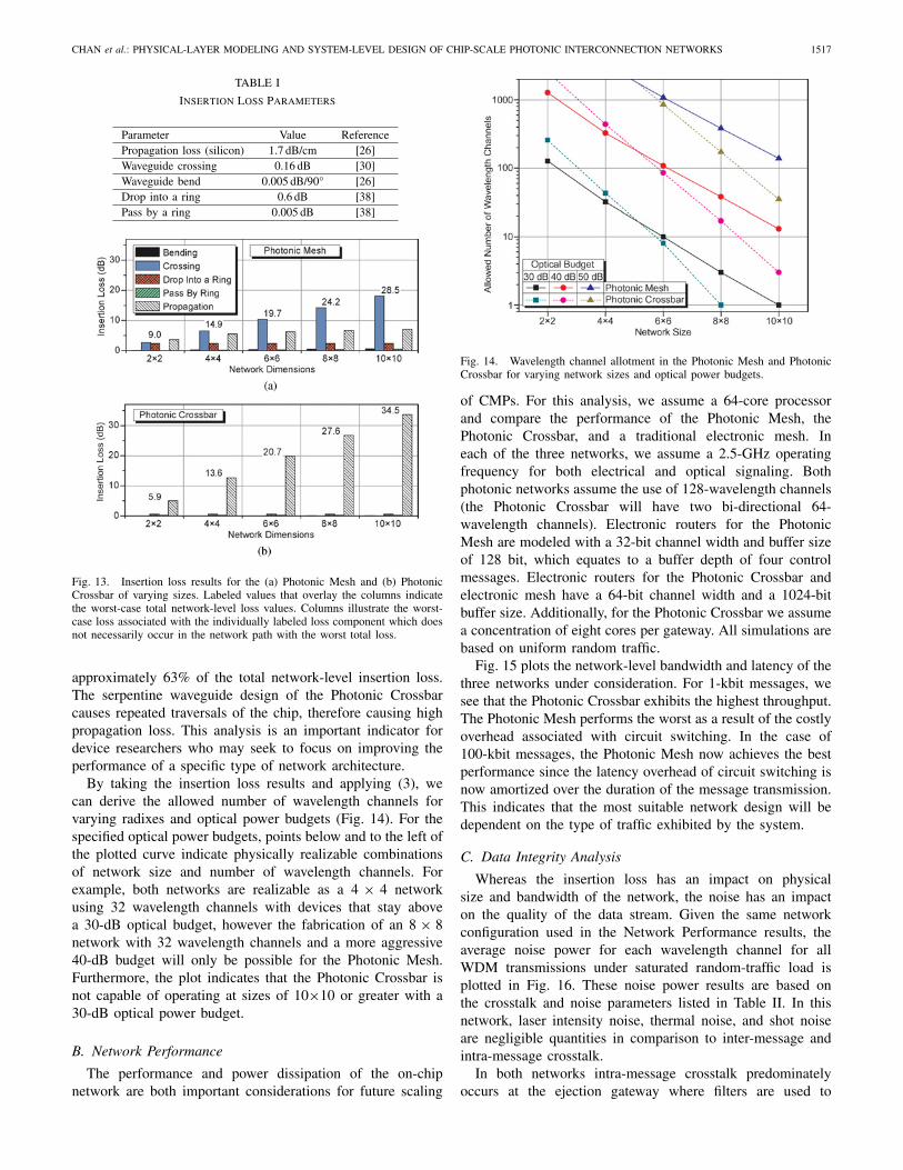
By taking the insertion loss results and applying (3), wecan derive the allowed number of wavelength channels forvarying radixes and optical power budgets (Fig. 14). For thespecified optical power budgets, points below and to the left ofthe plotted curve indicate physically realizable combinationsof network size and number of wavelength channels. Forexample, both networks are realizable as a 4 × 4 networkusing 32 wavelength channels with devices that stay abovea 30-dB optical budget, however the fabrication of an 8 × 8network with 32 wavelength channels and a more aggressive40-dB budget will only be possible for the Photonic Mesh.Furthermore, the plot indicates that the Photonic Crossbar isnot capable of operating at sizes of 10×10 or greater with a30-dB optical power budget.
B. Network Performance
The performance and power dissipation of the on-chipnetwork are both important considerations for future scaling
Fig. 14. Wavelength channel allotment in the Photonic Mesh and PhotonicCrossbar for varying network sizes and optical power budgets.
of CMPs. For this analysis, we assume a 64-core processorand compare the performance of the Photonic Mesh, thePhotonic Crossbar, and a traditional electronic mesh. Ineach of the three networks, we assume a 2.5-GHz operatingfrequency for both electrical and optical signaling. Bothphotonic networks assume the use of 128-wavelength channels(the Photonic Crossbar will have two bi-directional 64-wavelength channels). Electronic routers for the PhotonicMesh are modeled with a 32-bit channel width and buffer sizeof 128 bit, which equates to a buffer depth of four controlmessages. Electronic routers for the Photonic Crossbar andelectronic mesh have a 64-bit channel width and a 1024-bitbuffer size. Additionally, for the Photonic Crossbar we assumea concentration of eight cores per gateway. All simulations arebased on uniform random traffic.
Fig. 15 plots the network-level bandwidth and latency of thethree networks under consideration. For 1-kbit messages, wesee that the Photonic Crossbar exhibits the highest throughput.The Photonic Mesh performs the worst as a result of the costlyoverhead associated with circuit switching. In the case of100-kbit messages, the Photonic Mesh now achieves the bestperformance since the latency overhead of circuit switching isnow amortized over the duration of the message transmission.This indicates that the most suitable network design will bedependent on the type of traffic exhibited by the system.
C. Data Integrity Analysis
Whereas the insertion loss has an impact on physicalsize and bandwidth of the network, the noise has an impacton the quality of the data stream. Given the same networkconfiguration used in the Network Performance results, theaverage noise power for each wavelength channel for allWDM transmissions under saturated random-traffic load isplotted in Fig. 16. These noise power results are based onthe crosstalk and noise parameters listed in Table II. In thisnetwork, laser intensity noise, thermal noise, and shot noiseare negligible quantities in comparison to inter-message andintra-message crosstalk.
In both networks intra-message crosstalk predominatelyoccurs at the ejection gateway where filters are used to

1518 IEEE TRANSACTIONS ON COMPUTER-AIDED DESIGN OF INTEGRATED CIRCUITS AND SYSTEMS, VOL. 30, NO. 10, OCTOBER 2011
Fig. 15. Bandwidth and latency performance on the Electronic Mesh,Photonic Crossbar, and Photonic Mesh for (a) 1-kbit and (b) 100-kbit messagesizes.
select individual wavelength channels. The amount of intra-message crosstalk power exhibited by each optical messageis predominately dependent on the number of co-propagatingwavelengths. Therefore, it is practically independent of bothnetwork load and message size. We see that across the twodifferent message sizes, the amount of intra-message crosstalkpower remains approximately constant.
The trend in inter-message crosstalk reflects the probabilitythat two WDM messages will intersect in the network.The Photonic Crossbar exhibits zero inter-message crosstalksince it contains no crossings or switches where a messageintersection could occur. A longer duration optical packet fromusing fewer wavelength channels or large message sizes willcreate a scenario where the photonic message will occupythe network for a longer period of time, thereby increasingthe likelihood that another message will be instanced in thenetwork and interfere. In Fig. 16, we can see that indeed largermessages in the Photonic Mesh do produce a non-negligibleamount of inter-message crosstalk.
Lastly, PhoenixSim also determines the signals SNR whenthe message is finally received. For 1-kbit message sizes, theaverage electrical SNR of the Photonic Mesh and PhotonicCrossbar optical link is 6.4 dB and 3.5 dB, respectively. For100-kbit message sizes, the average SNR for the PhotonicMesh and Photonic Crossbar is 6.5 dB and 2.9 dB, respectively.These results indicate that the Photonic Crossbar relativelyoutperforms the Photonic Mesh with respect to signal integrity.However these values also conclude that the optical linkintegrity of both networks will be detrimentally compromised.This performance penalty can be rectified by improved filterperformance or through the use of fewer wavelength channels.
D. Power Dissipation Analysis
Last, we compare the power dissipation of the ElectronicMesh, Photonic Mesh, and Photonic Crossbar, assuming the
TABLE II
Crosstalk and Noise Parameters
Parameter Value ReferenceLaser (relative intensity noise) −150 dB/Hz [43]Modulator (extinction ratio) 16 dB [46]PSE through-port (extinction ratio) 25 dB [38]PSE drop-port (extinction ratio) 20 dB [38]Waveguide crossing (crosstalk) −40 dB [30]
Fig. 16. Average total noise power accumulated by each optical message inthe Photonic Mesh and Photonic Crossbar for saturated network load. Lasernoise, thermal noise, and shot noises are negligible quantities and are notlisted.
same system configuration as before and the power parameterslisted in Table III. The total power dissipation of eachnetwork, operating with maximum load, is plotted in Fig. 17.Each column is broken down into categories of photonic-related dissipation from ring modulators, photodetectors,optical switches, and thermal feedback tuning, and electronic-related dissipation from router logic, router buffers, andwires. While SerDes would be required in many proposedphotonic interconnect architectures for every ring modulatorand photodetector to up and down convert to the photonictransmission clock, in this case study we assume the same2.5-GHz clock for both electronic and photonic domains.
Regardless of the message size the Electronic Meshdissipates approximately 8 W of power and the PhotonicMesh dissipates approximately 5 W. This is a result of bothnetworks relying on some electronic routers to route data.Data on the Photonic Mesh is only transmitted optically,which provides a significant savings in power when thecircuit-switching overhead can be amortized. In terms ofenergy efficiency when transmitting 1-kbit messages, thePhotonic Crossbar outperforms the other networks at 2.9 pJ/bit,while the Photonic Mesh performs the worst at 55.9 fJ/bit.Nonetheless, with the larger 100-kbit messages, the PhotonicMesh achieves the highest efficiency with 3.2 pJ/bit as aresult of the efficient optical transmission. This message-size/efficiency relationship of the circuit-switched PhotonicMesh design is a useful indicator as to which photonic designmay be ideally suited for various application traffic patterns.

CHAN et al.: PHYSICAL-LAYER MODELING AND SYSTEM-LEVEL DESIGN OF CHIP-SCALE PHOTONIC INTERCONNECTION NETWORKS 1519
TABLE III
Power Dissipation Parameters
Parameter ValueModulators (dynamic energy) 85 fJ/bitModulators (static energy) 30 μWPhotodetectors 50 fJ/bitPSEs (dynamic energy) 375 fJ/bitPSEs (static energy) 400 μWThermal ring tuning 100 μW/ring
Fig. 17. Network-level power dissipation breakdown of the Electronic Mesh,Photonic Mesh, and Photonic Crossbar for transmission of 1-kbit and100-kbit messages. Values overlaying each column indicate the energyefficiency of the network in units of pJ/bit.
For instance, photonic circuits have been shown to be ideallysuited for many classes of scientific applications that requirelong data messages [15].
VII. Conclusion
We have described a methodology for modeling, designing,and analyzing photonic interconnection networks at both thephysical-layer and system-level. A Photonic Device Libraryhas been devised to describe any type of fundamental photonicelements, which can then be combined and used to modellarge-scale photonic components and network topologies.We developed a set of physical-layer tools to accuratelydetermine physical properties of the photonic networks andexamine how they impact the network architectures interms of system performance. Our PhoenixSim environmentimplements this methodology, which we have made opensource and publicly available. We illustrated the capabilitiesof PhoenixSim through the analysis of two photonic networksand showed how various system-level design tradeoffs aremade possible through an understanding of the physical-layer characteristics. The device library, analysis tools, andsimulation environment form a comprehensive design flow forunderstanding and designing photonically enabled computingsystems.
References
[1] D. Miller, “Device requirements for optical interconnects tosilicon chips,” Proc. IEEE, vol. 97, no. 7, pp. 1166–1185, Jul.2009.
[2] N. Magen, A. Kolodny, U. Weiser, and N. Shamir, “Interconnect-powerdissipation in a microprocessor,” in Proc. Int. Workshop SLIP, Feb. 2004,pp. 7–13.
[3] Photonic and Electronic Network Integration and Execution Simulator(PhoenixSim) [Online]. Available: http://lightwave.ee.columbia.edu/phoenixsim
[4] A. Varga. OMNeT++ Discrete Event Simulation System [Online].Available: http://www.omnetpp.org
[5] J. Chan, G. Hendry, A. Biberman, K. Bergman, and L. Carloni,“PhoenixSim: A simulator for physical-layer analysis of chip-scalephotonic interconnection networks,” in Proc. DATE, Mar. 2010, pp. 691–696.
[6] D. Vantrease, R. Schreiber, M. Monchiero, M. McLaren, N. P. Jouppi,M. Fiorentino, A. Davis, N. Binkert, R. G. Beausoleil, and J. H. Ahn,“Corona: System implications of emerging nanophotonic technology,”in Proc. 35th Annu. ISCA, Jun. 2008, pp. 153–164.
[7] A. Joshi, C. Batten, Y.-J. Kwon, S. Beamer, I. Shamim, K. Asanovic,and V. Stojanovic, “Silicon-photonic Clos networks for global on-chipcommunication,” in Proc. 3rd ACM/IEEE Int. NOCS, May 2009, pp.124–133.
[8] Y. Pan, P. Kumar, J. Kim, G. Memik, Y. Zhang, and A. Choudhary,“Firefly: Illuminating future network-on-chip with nanophotonics,” inProc. 36th Annu. ISCA, Jun. 2009, pp. 429–440.
[9] N. Kirman, M. Kirman, R. K. Dokania, J. F. Martinez, A. B.Apsel, M. A. Watkins, and D. H. Albonesi, “Leveraging opticaltechnology in future bus-based chip multiprocessors,” in Proc. 39thAnnu. IEEE/ACM Int. Symp. Microarch. (MICRO), Dec. 2006, pp. 492–503.
[10] C. Batten, A. Joshi, J. Orcutt, A. Khilo, B. Moss, C. W. Holzwarth,M. A. Popovic, H. Li, H. I. Smith, J. L. Hoyt, F. X. Kartner, R. J.Ram, V. Stojanovic, and K. Asanovic, “Building many-core processor-to-DRAM networks with monolithic CMOS silicon photonics,” IEEEMicro, vol. 29, no. 4, pp. 8–21, Jul.–Aug. 2009.
[11] M. J. Cianchetti, J. C. Kerekes, and D. H. Albonesi, “Phastlane: A rapidtransit optical routing network,” in Proc. 36th Annu. ISCA, Jun. 2009,pp. 441–450.
[12] A. Shacham, K. Bergman, and L. P. Carloni, “Photonic networks-on-chipfor future generations of chip multiprocessors,” IEEE Trans. Comput.,vol. 57, no. 9, pp. 1246–1260, Sep. 2008.
[13] M. Petracca, B. G. Lee, K. Bergman, and L. P. Carloni, “Photonic NoCs:System-level design exploration,” IEEE Micro, vol. 29, no. 4, pp. 74–85,Aug. 2009.
[14] J. Chan, G. Hendry, A. Biberman, and K. Bergman, “Architecturalexploration of chip-scale photonic interconnection network designs usingphysical-layer analysis,” J. Lightw. Technol., vol. 28, no. 9, pp. 1305–1315, May 2010.
[15] G. Hendry, S. Kamil, A. Biberman, J. Chan, B. Lee, M. Mohiyuddin,A. Jain, K. Bergman, L. Carloni, J. Kubiatowicz, L. Oliker, and J. Shalf,“Analysis of photonic networks for a chip multiprocessor using scientificapplications,” in Proc. 3rd ACM/IEEE Int. NOCS, May 2009, pp. 104–113.
[16] G. Hendry, J. Chan, S. Kamil, L. Oliker, J. Shalf, L. Carloni,and K. Bergman, “Silicon nanophotonic network-on-chip usingTDM arbitration,” in Proc. 18th Annu. IEEE Symp. High Perform.Interconnects (HOTI), Aug. 2010, pp. 88–95.
[17] D. Ding and D. Z. Pan, “OIL: A nano-photonics optical interconnectlibrary for a new photonic networks-on-chip architecture,” in Proc. 11thInt. Workshop SLIP, Jul. 2009, pp. 11–18.
[18] J. Minz, S. Thyagaraja, and S. K. Lim, “Optical routing for 3D system-on-package,” in Proc. DATE, vol. 1. Mar. 2006, pp. 1–2.
[19] G. Hendry, J. Chan, L. P. Carloni, and K. Bergman, “VANDAL: A toolfor the design specification of nanophotonic networks,” in Proc. DATE,Mar. 2011, pp. 1–6.
[20] I. O’Connor, F. Tissafi-Drissi, F. Gaffiot, J. Dambre, M. D. Wilde,J. V. Campenhout, D. V. Thourhout, J. V. Campenhout, andD. Stroobandt, “Systematic simulation-based predictive synthesis ofintegrated optical interconnect,” IEEE Trans. Very Large Scale Integr.Syst., vol. 15, no. 8, pp. 927–940, Aug. 2007.
[21] M. De Wilde, O. Rits, W. Meeus, H. Lambrecht, and J. V. Campenhout,“Integration of modeling tools for parallel optical interconnects in astandard EDA design environment,” in Proc. DATE, Feb. 2004 [Online].Available: http://citeseerx.ist.psu.edu/viewdoc/summary

1520 IEEE TRANSACTIONS ON COMPUTER-AIDED DESIGN OF INTEGRATED CIRCUITS AND SYSTEMS, VOL. 30, NO. 10, OCTOBER 2011
[22] P. K. Pepeljugoski and D. M. Kuchta, “Design of opticalcommunications data links,” IBM J. Res. Dev., vol. 47, nos. 2–3, pp.223–237, Mar. 2003.
[23] M. Briere, E. Drouard, F. Mieyeville, D. Navarro, I. O’Connor, andF. Gaffiot, “Heterogeneous modelling of an optical network-on-chipwith SystemC,” in Proc. 16th IEEE Int. Workshop RSP, Jun. 2005,pp. 10–16.
[24] A. Kodi and A. Louri, “Optisim: A system simulation methodology foroptically interconnected HPC systems,” IEEE Micro, vol. 28, no. 5, pp.22–36, Sep.–Oct. 2008.
[25] H.-S. Wang, X. Zhu, L.-S. Peh, and S. Malik, “Orion: A power-performance simulator for interconnection networks,” in Proc. 35thAnnu. ACM/IEEE Int. Symp. Microarch. (MICRO), Nov. 2002, pp. 294–305.
[26] F. Xia, L. Sekaric, and Y. Vlasov, “Ultracompact optical buffers on asilicon chip,” Nature Photonics, vol. 1, pp. 65–71, Dec. 2006.
[27] M. Gnan, S. Thorns, D. Macintyre, R. D. L. Rue, and M. Sorel,“Fabrication of low-loss photonic wires in silicon-on-insulator usinghydrogen silsesquioxane electron-beam resist,” IET Electron. Lett.,vol. 44, no. 2, pp. 115–116, Jan. 2008.
[28] J. Cardenas, C. B. Poitras, J. T. Robinson, K. Preston, L. Chen, andM. Lipson, “Low loss etchless silicon photonic waveguides,” OSA OpticsExpress, vol. 17, no. 6, pp. 4752–4757, 2009.
[29] M. J. Shaw, J. Guo, G. A. Vawter, S. Habermehl, and C. T. Sullivan,“Fabrication techniques for low-loss silicon nitride waveguides,”Micromach. Technol. Micro-Optics Nano-Optics III, vol. 5720, pp. 109–118, 2005.
[30] W. Bogaerts, P. Dumon, D. V. Thourhout, and R. Baets, “Low-loss, low-cross-talk crossings for silicon-on-insulator nanophotonic waveguides,”OSA Optics Lett., vol. 32, no. 19, pp. 2801–2803, 2007.
[31] V. R. Almeida, R. R. Panepucci, and M. Lipson, “Nanotaper for compactmode conversion,” OSA Optics Lett., vol. 28, no. 15, pp. 1302–1304,2003.
[32] G. Roelkens, D. V. Thourhout, and R. Baets, “High efficiency gratingcoupler between silicon-on-insulator waveguides and perfectly verticaloptical fibers,” OSA Optics Lett., vol. 32, no. 11, pp. 1495–1497,2007.
[33] M. Lipson, “Compact electro-optic modulators on a silicon chip,” IEEEJ. Selected Topics Quantum Electron., vol. 12, no. 6, pp. 1520–1526,Nov.–Dec. 2006.
[34] W. Green, H. Hamann, L. Sekaric, M. Rooks, and Y. Vlasov, “Ultra-compact reconfigurable silicon optical devices using micron-scalelocalized thermal heating,” in Proc. OFC, Mar. 2007, p. OTuM3.
[35] M. Watts, D. Trotter, R. Young, and A. Lentine, “Ultralow power siliconmicrodisk modulators and switches,” in Proc. 5th IEEE Int. Conf. GroupIV Photonics, Sep. 2008, pp. 4–6.
[36] Q. Xu, S. Manipatruni, B. Schmidt, J. Shakya, and M. Lipson, “12.5Gbit/s carrier-injection-based silicon micro-ring silicon modulators,”OSA Optics Express, vol. 15, no. 2, pp. 430–436, 2007.
[37] Y. Vlasov, W. M. J. Green, and F. Xia, “High-throughputsilicon nanophotonic wavelength-insensitive switch for on-chip opticalnetworks,” Nat. Photonics, vol. 2, pp. 242–246, Apr. 2008.
[38] B. G. Lee, A. Biberman, P. Dong, M. Lipson, and K. Bergman, “All-optical comb switch for multiwavelength message routing in siliconphotonic networks,” IEEE Photonics Technol. Lett., vol. 20, no. 10, pp.767–769, May 2008.
[39] B. Little, J. Foresi, G. Steinmeyer, E. Thoen, S. Chu, H. Haus, E. Ippen,L. Kimerling, and W. Greene, “Ultra-compact Si-SiO2 microringresonator optical channel dropping filters,” IEEE Photonics Technol.Lett., vol. 10, no. 4, pp. 549–551, Apr. 1998.
[40] S. Assefa, F. Xia, S. W. Bedell, Y. Zhang, T. Topuria, P. M. Rice,and Y. A. Vlasov, “CMOS-integrated 40 GHz germanium waveguidephotodetector for on-chip optical interconnects,” in Proc. OFC, Mar.2009, p. OMR4.
[41] L. Vivien, J. Osmond, J.-M. Fedeli, D. Marris-Morini, P. Crozat,J.-F. Damlencourt, E. Cassan, Y. Lecunff, and S. Laval, “42 GHzp.i.n germanium photodetector integrated in a silicon-on-insulatorwaveguide,” OSA Optics Express, vol. 17, no. 8, pp. 6252–6257,2009.
[42] H.-W. Chen, Y.-H. Kuo, and J. E. Bowers, “High speed hybrid siliconevanescent Mach–Zehnder modulator and switch,” OSA Optics Express,vol. 16, no. 25, pp. 20571–20576, 2008.
[43] T. Gensty, W. Elsaßer, and C. Mann, “Intensity noise properties ofquantum cascade lasers,” OSA Optics Express, vol. 13, no. 6, pp. 2032–2039, 2005.
[44] C. Miller, Fiber Optic Test and Measurement. Englewood Cliffs, NJ:Prentice-Hall, 1998.
[45] J. Chan, A. Biberman, B. Lee, and K. Bergman, “Insertion lossanalysis in a photonic interconnection network for on-chip and off-chipcommunications,” in Proc. 21st Annu. Meeting IEEE LEOS, Nov. 2008,pp. 300–301.
[46] K. Preston, S. Manipatruni, A. Gondarenko, C. B. Poitras, andM. Lipson, “Deposited silicon high-speed integrated electro-opticmodulator,” OSA Optics Express, vol. 17, no. 7, pp. 5118–5124, 2009.
Johnnie Chan (S’08) received the B.S. degree (highdistinction) in computer and electrical engineeringand the M.S. degree in electrical engineering fromthe University of Virginia, Charlottesville, in 2005and 2007, respectively. He is currently pursuingthe Ph.D. degree with the Department of ElectricalEngineering, Columbia University, New York, NY.
His current research interests include siliconphotonic devices for chip-scale interconnectionnetworks and optical networks for high-performancecomputing.
Gilbert Hendry (S’08) received the B.S. and M.S.degrees in computer engineering from the RochesterInstitute of Technology, Rochester, NY, in 2007,and the Ph.D. degree from Columbia University,New York, NY, in 2011.
He is currently a Post-Doctoral Researcher withthe Department of Scalable Modeling and Analysis,Sandia National Laboratories, Livermore, CA.His current research interests include modeling,simulation, layout, and design automation ofchip-scale networks, particularly those using
nanophotonics.
Keren Bergman (S’87–M’93–SM’07–F’09) recei-ved the B.S. degree from Bucknell University,Lewisburg, PA, in 1988, and the M.S. andPh.D. degrees from the Massachusetts Institute ofTechnology, Cambridge, in 1991 and 1994, respecti-vely, all in electrical engineering.
She is currently a Professor and Chair of theDepartment of Electrical Engineering, ColumbiaUniversity, New York, NY, where she alsodirects the Lightwave Research Laboratory. Sheleads multiple research programs on optical
interconnection networks for advanced computing systems, data centers,optical packet switched routers, and chip multiprocessor nanophotonicnetworks-on-chip.
Dr. Bergman is a fellow of the OSA and currently serves as the Co-Editor-in-Chief of the IEEE/OSA Journal of Optical Communications and Networking.
Luca P. Carloni (S’95–M’04–SM’09) received theLaurea degree (summa cum laude) in electricalengineering from the Universita di Bologna,Bologna, Italy, in 1995, and the M.S. and Ph.D.degrees in electrical engineering and computersciences from the University of California, Berkeley,in 1997 and 2004, respectively.
He is currently an Associate Professor withthe Department of Computer Science, ColumbiaUniversity, New York, NY. He has authored over 80publications and is the holds one patent. His current
research interests include design methodologies and tools for integratedcircuits and systems, distributed embedded systems design, and design ofhigh-performance computer systems.
Dr. Carloni received the Faculty Early Career Development (CAREER)Award from the National Science Foundation in 2006, was selected as anAlfred P. Sloan Research Fellow in 2008, and received the ONR YoungInvestigator Award in 2010. He is the recipient of the 2002 Demetri AngelakosMemorial Achievement Award for “recognition of altruistic attitude towardfellow graduate students.” In 2002, one of his papers was selected for the“Best of ICCAD,” a collection of the best IEEE International Conference onComputer-Aided Design papers of the past 20 years. He is a Senior Memberof the Association for Computing Machinery.