physical optics and electronics - rle at mit
TRANSCRIPT

Chapter 30. Physical Optics and Electronics
30-1
Physical Optics and Electronics Academic and Research Staff Professor Rajeev J. Ram, Dr. Xiaoyun Guo, Dr. Harry Lee, Elizabeth Bruce Graduate Students Reja Amatya, Kevin Lee, Tom Liptay, Peter Mayer, Jason Orcutt, Tauhid Zaman Technical and Support Staff Catherine Bourgeois Overview The research in the Physical Optics and Electronics Group is divided along three primary themes:
• Integrated Photonics • Biophotonics and Bioprocessors • Thermodynamics of Semiconductor Devices
In all three areas the goal of this research is to exploit processes in physics to invent new devices that lead to better systems. Each researcher works to model and design a new device, implement the design, and then integrated this device into a system which defines the state-of-the-art. The major achievements of the laboratory during the last year were: The demonstration
1. Fabrication of zero-birefringence InP waveguides with large Faraday rotation. 2. Spatially resolved measurements of perimeter degradation in Ge-on-Si detectors. 3. Design of record low-power tunable microring filter in SiN. 4. Demonstration of 3-D polymer waveguide circuits. The waveguides were used to
illustrate frequency-domain multiplexing of a sensor array. 5. Demonstration of a microfluidic mixer with shear control enabling the culture of
mammalian cells (Chinese Hamster Ovary cells). 6. Completion of a technology needs-assessment for the biopharmaceutical industry. 7. Design of high power thermoelectric generator employing microchannel cooling.

Chapter 30. Physical Optics and Electronics
30-2 RLE Progress Report 149
Cell Culture in Parallel Integrated Bioreactor Arrays Sponsor MIT Lincoln Laboratory MIT-Malaysia Program Project Staff Harry Lee, Professor Rajeev J. Ram Paolo Boccazzi, Professor Anthony J. Sinskey Cell culture and microbial fermentation technology has largely remained unchanged for the past half-century. Using bench scale stirred tank bioreactors, shake flasks, or shaken microtiter plates, scientists have always faced a tradeoff between quality and quantity while conducting experiments to explore a large parameter space. Even recently developed cell culture systems have not eliminated this tradeoff, having instead inherited the limitations of their predecessors. Our research has focused on introducing entirely new approaches to creating a cell culture or fermentation system using microfluidic hybrid integration. This technology platform combines novel fluidic devices, mass producible manufacturing processes, and sensor technologies to enable an entirely different bioreactor design. The design flexibility afforded by the microfluidic integration platform opens the possibility for application specific bioreactor design. Through customization of bioreactor devices, higher performance can be achieved by eliminating compromises required for general purpose instruments. Since our early proof-of-concept bioreactors, we have made four significant advances: First, we solved a key fabrication problem to enable a more flexible and robust manufacturing process that is more amenable to mass production. Second, we developed fluid injection ports which are compatible with conventional laboratory pipettes that greatly simplify fluid injection and removal. Third, we have improved the precision of the fluid injectors. Finally, we have developed alternative mixing devices that generate lower shear forces for mammalian cell culture and permit independent control over dissolved gas concentrations.
Fig. 1: Photograph of a section of a new bioreactor device using the improved fabrication process and incorporating new fluid injection ports, high precision fluid injectors, and new mixing devices.

Chapter 30. Physical Optics and Electronics
30-3
Polymer Waveguides for Integrated Biosensors Sponsor NSF Center for Materials Science and Engineering MIT Malaysia Program Project Staff Kevin Lee, Professor Rajeev J. Ram To provide sensors for truly portable lab-on-a-chip systems, optical detection must be made compact and cheap, utilizing non-imaging optics such as waveguides and reducing off-chip components such as photodetectors and photomultiplier tubes. Many different approaches to waveguide fabrication have been demonstrated for integration with microfluidic systems [1, 2, 3]. In addition, frequency division multiplexing (FDM) has been explored as a method to reduce component costs and increase speed for multichannel fluorescence microscopes [4]. By combining waveguides with frequency multiplexed fluorescence detection, a low cost and scalable approach for accurate detection of multiple fluorescence signals located within a single chip is possible. By fabricating waveguides with conventional machining, 3-dimensional profiles such as vertical couplers are possible. In addition, by making multiple layer stacks, waveguides can be densely routed to detectors. A test chip demonstrating frequency multiplexed detection is shown in Figure 1. Using a three layer fabrication process, excitation waveguides can be used to excite sensors in a biochip. These can then be collected by vertical waveguides which direct the collected fluorescence into either layer 2 or layer 3, where vertical bends deflect the light in to be combined and detected by a photodetector. To demonstrate the detection system, four different fluorescent sensors are placed at the detection sites of the waveguide backplane. As shown in Figure 2, the overlapping spectra of the different sensors make simultaneous measurements difficult in wavelength domain. However, by utilizing individual modulation frequencies for sensor excitation, the measured signal at the photodetector can be easily demultiplexed in frequency domain as shown in Figure 3. FDM is able to extract data from the sensors despite the large overlap in emission between different fluorophors.
Figure 1. Schematic of the multilayer waveguide backplane used for demonstrating frequency division multiplexed fluorescence detection.

Chapter 30. Physical Optics and Electronics
30-4 RLE Progress Report 149
(a) (b)
Figure 2. (a) Emission spectra of the waveguide output incident on the photodetector. Oxygen and pH are still distinguishable with frequency multiplexing under large spectral interference. (b) Power spectral density of the output photodetector clearly indicating the modulation frequencies of each fluorophor. [1] C. H. Lin, G. B. Lee, G. L. Chang, “Micro flow cytometers integrated with buried SU-8/SOG
optical waveguides,” Sensors Actuators A, 130, 165–70 (2003). [2] J. Khandurina, T. E. McKnight, S. C. Jacobson, L. C. Waters, R. S. Foote, J. M. Ramsey,
“Integrated System for Rapid PCR-Based DNA Analysis in Microfluidic Devices," Anal. Chem., 72, 2995-3000 (2000).
[3] D. A. Chang-Yen, B. K. Gale, “An integrated optical oxygen sensor fabricated using rapid-prototyping techniques”, Lab Chip, 3, 297-301, (2003).
[4] F. Wu, X. Zhang, J. Y. Cheung, K. Shi, Z. Liu, C. Luo, S. Yin, P. Ruffin, “Frequency Division Multiplexed Multichannel High-Speed Fluorescence Confocal Microscope,” Biophys. J., 91, 2290-2296 (2006)
Chapter 30. Physical Optics and Electronics
30-5
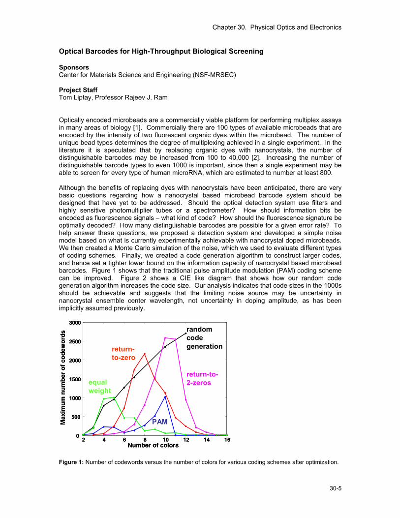
Optical Barcodes for High-Throughput Biological Screening Sponsors Center for Materials Science and Engineering (NSF-MRSEC) Project Staff Tom Liptay, Professor Rajeev J. Ram Optically encoded microbeads are a commercially viable platform for performing multiplex assays in many areas of biology [1]. Commercially there are 100 types of available microbeads that are encoded by the intensity of two fluorescent organic dyes within the microbead. The number of unique bead types determines the degree of multiplexing achieved in a single experiment. In the literature it is speculated that by replacing organic dyes with nanocrystals, the number of distinguishable barcodes may be increased from 100 to 40,000 [2]. Increasing the number of distinguishable barcode types to even 1000 is important, since then a single experiment may be able to screen for every type of human microRNA, which are estimated to number at least 800. Although the benefits of replacing dyes with nanocrystals have been anticipated, there are very basic questions regarding how a nanocrystal based microbead barcode system should be designed that have yet to be addressed. Should the optical detection system use filters and highly sensitive photomultiplier tubes or a spectrometer? How should information bits be encoded as fluorescence signals – what kind of code? How should the fluorescence signature be optimally decoded? How many distinguishable barcodes are possible for a given error rate? To help answer these questions, we proposed a detection system and developed a simple noise model based on what is currently experimentally achievable with nanocrystal doped microbeads. We then created a Monte Carlo simulation of the noise, which we used to evaluate different types of coding schemes. Finally, we created a code generation algorithm to construct larger codes, and hence set a tighter lower bound on the information capacity of nanocrystal based microbead barcodes. Figure 1 shows that the traditional pulse amplitude modulation (PAM) coding scheme can be improved. Figure 2 shows a CIE like diagram that shows how our random code generation algorithm increases the code size. Our analysis indicates that code sizes in the 1000s should be achievable and suggests that the limiting noise source may be uncertainty in nanocrystal ensemble center wavelength, not uncertainty in doping amplitude, as has been implicitly assumed previously.
2 4 6 8 10 12 14 160
500
1000
1500
2000
2500
3000
Number of colors
Max
imum
num
ber
of c
odew
ords
return-to-zero
randomcodegeneration
return-to-2-zerosequal
weight
PAM
2 4 6 8 10 12 14 160
500
1000
1500
2000
2500
3000
Number of colors
Max
imum
num
ber
of c
odew
ords
return-to-zero
randomcodegeneration
return-to-2-zerosequal
weight
PAM
Figure 1: Number of codewords versus the number of colors for various coding schemes after optimization.

Chapter 30. Physical Optics and Electronics
30-6 RLE Progress Report 149
-1 0 1
0
1
PAM - 4 levels (0,1,2,3)
-1 0 1
0
1
Equal Weight – weight 9
-1 0 1
0
1
Random – 100 levels
(100)
(010)
(001)
(111)
(031)(021)(032)
(072)(162)(063)(153)(054)
(131)
-1 0 1
0
1
PAM - 4 levels (0,1,2,3)
-1 0 1
0
1
Equal Weight – weight 9
-1 0 1
0
1
Random – 100 levels
-1 0 1
0
1
PAM - 4 levels (0,1,2,3)
-1 0 1
0
1
PAM - 4 levels (0,1,2,3)
-1 0 1
0
1
Equal Weight – weight 9
-1 0 1
0
1
Equal Weight – weight 9
-1 0 1
0
1
Random – 100 levels
-1 0 1
0
1
Random – 100 levels
(100)
(010)
(001)
(111)
(031)(021)(032)
(072)(162)(063)(153)(054)
(131)
Figure 2: CIE plot for 3 color codes. The noise has a different magnitude and shape in different regions. Top – PAM coding scheme with 4 levels (0, 1, 2, and 3). Middle – PAM with the constraint that the weight (sum of the desired amplitudes) of each codeword equals 9. Bottom – Results of the random code generation algorithm. The random code generation algorithm allows codes to be spaced more densely in regions that are less sensitive to noise. [1] www.luminex.com [2] M. Han, X. Gao, J. Z. Su, and S. Nie, "Quantum-dot-tagged microbeads for multiplexed optical coding of biomolecules," nat. biotechnol., vol. 19, pp. 631, 2001.
Chapter 30. Physical Optics and Electronics
30-7
Biomanufacturing Industry Needs Assesment Sponsors Center for Biomedical Innovation Bayer Corporation Project Staff Elizabeth Bruce, Dr. Harry Lee, Dr. Paolo Boccazzi, Professor Rajeev J. Ram, Professor Anthony J. Sinskey The primary objective of this project is to articulate the critical challenges facing the biopharmaceutical manufacturing industry as identified in a series of industry interviews of pharmaceutical and industrial biomanufacturers. The output of this study enables us to identify and develop strategic projects within CBI that target specific industry challenges and leverage MIT’s research strengths in developing new tools for the biomanufacturing industry. The methodology used in this study utilizes a set of systematic tools and processes for gathering and processing large amounts of qualitative information1. We completed a series of interviews, including site visits and manufacturing tours, at 11 different manufacturing organizations. Challenges were identified in six primary areas, in summary: A. Optimizing the expression system. Improving the expression system to optimize productivity and simplify product characterization can significantly delay time to market. In particular, for mammalian cell cultures, heterogeneity of the culture makes it difficult to characterize. B. Improving Product-Process Characterization. Limited understanding of the correlation mechanisms between manufacturing process and product make it difficult to reduce cycle times and improve efficiency; Characterizing protein stability, which requires testing the product at higher temperatures, is time-consuming and often increases time to clinical trials; Product characterization requires expensive off-line analytical instruments (ex. mass spec, hplc) which often causes delays in manufacturing process; Many online sensors, including conventional probes (T, pH) and optical (NIR, fluorescence), are not seen as reliable or robust enough for the manufacturing environment. C. Speeding Process Development. Functional scale down models do not extend throughout entire process flow due to 1) insufficient volume for analytical testing, 2) mismatch in capacity requirements between upstream and downstream processes, and 3) limitations of predictive modeling for scale up. In addition, current screening processes for strain selection are time consuming and labor intensive. D. Streamlining Purification. Purification is increasingly the processing bottleneck both at small (pre-clinical trials) and larger (production) volumes, issues include: Reliance on Protein A, due to limited alternatives; Chromatography columns difficult to scale to larger volumes; Difficulty in obtaining high levels of purity at early stage for clinical trials. E. Streamlining Plant Design and Operations. Many biomanufacturing plants operate below maximum efficiency due to 1) regulatory and clinical trial processes; 2) errors in design modeling; 3) inefficiencies in moving media and product through plant. In addition, it is often difficult for manufacturers to reliably detect contamination in fermentation tanks to know when to terminate a batch early to minimize operating losses. F. Changing Industry/Regulatory Dynamics. Manufacturers tend to be risk averse when it comes to adopting new sensor/measurement technologies as it is not always clear that the benefits outweigh the costs, including: Limited information available on the benefits of Process Analytical Technology (PAT) implementations; Characterizing new sensors and their failure modes can take up to 2-5 years; Fear that new approach not accepted by FDA. 1 methodology based on TQM tools, see Voices into Choices: Acting on the Voice of the Customer, Center for Quality Management, Gary Burchill and Christina Hepner Brodie, 1997

Chapter 30. Physical Optics and Electronics
30-8 RLE Progress Report 149
Faraday Rotation in InP Waveguide Devices Sponsor MIT Lincoln Laboratory Integrated Photonics Initiative Project Staff Tauhid Zaman, Dr. Xiaoyun Guo, Professor Rajeev Ram
The demonstration of waveguide isolators and circulators that can easily be integrated with active and passive optical components is essential to large scale photonic integration. Not only do these components provide functionality that cannot be achieved in integrated circuits today, but they also enable complex photonic circuit design by isolating or ‘buffering’ the various parts of a circuit. We have demonstrated that Faraday rotators – a central component in bulk isolators and circulators – can be fabricated from Fe:InP and Fe:InGaAsP. Realization of integrated Faraday rotators requires a waveguide where the two orthogonally polarized modes have nearly equal propagation constants (zero birefringence). The width of high-mesa waveguides can be etch-tuned to achieve zero birefringence [1]. The waveguides used here are high-mesa structures consisting of a 0.5 μm Fe:In1-xGaxAsyP1-y (x=0.290 and y=0.628) core layer and 1.0 μm Fe:InP cladding layers with an Fe doping of 8.0 x 1016 cm-3 in the core. The waveguide width for zero-birefringence at a wavelength of 1.55 μm is 1.4 μm [2]. Waveguides of different widths were fabricated with low pressure methane based reactive ion etching. To measure the waveguide Faraday rotation, a spinning magnet with an oscillating 50 mT magnetic field was used. The measured Verdet coefficient (rotation per length per magnetic field strength) and scanning electron micrographs (SEM’s) of the waveguides are shown in Figure 1. The theoretical curve was fit to the experimental curves using the modal Verdet coefficient as a fitting parameter. As can be seen, the rotation has a peak which corresponds to the zero birefringence wavelength for each waveguide. The zero birefringence wavelength is different because of the different widths of the waveguides. The location of these zero-birefringence peaks agree with theoretical predictions calculated using a commercial two dimensional mode solver. For these high-mesa waveguides, a 1 nm shift in width will shift the zero birefringence wavelength by approximately 1 nm.
The relevant figure of merit for a Faraday rotator is the ratio of the Faraday rotation coefficient (rotation per length) to the optical loss. A Faraday rotator is desired which provides 45 degrees of rotation, along with less than 1 dB of loss. The resulting figure of merit then becomes 45. The Verdet coefficient typically increases as the detuning of the optical wavelength from the bandgap decreases, and there are expressions for the Verdet coefficient as a function of this detuning [3]. There are two main sources of loss in the waveguides. The first is material absorption, and the second is scattering loss. The material loss can be approximated by an exponential decay given by the Urbach energy [4] and the scattering loss shows a 1/λ4 dependence [5]. Using a conservative estimate for the Urbach energy of Fe:InGaAsP [6,7] and the measured scattering loss, the resulting plot of the waveguide figure of merit in a 1 T magnetic field versus detuning of the optical wavelength from the bandgap of the InGaAsP core is show in Figure 2. As can be seen, when both loss mechanisms are considered, the target figure of merit can be achieved at a detuning of 0.1 μm.
The demonstration of Faraday rotation in a semiconductor waveguide shows that this nonreciprocal component does not need a magnetic garnet, but instead can be fabricated in a material compatible with conventional integrated photonic devices. This is a major step towards the achievement of monolithically integrated optical isolators and circulators.

Chapter 30. Physical Optics and Electronics
30-9
Figure 1: Experimental and theoretical modal Verdet coefficient for high-mesa Fe doped InP/InGaAsP waveguides. The theoretical curves are fit to the experimental curves using only the modal Verdet coefficient as a fitting parameter. The insets show SEM’s of the waveguides.
Figure 2: Figure of merit in a 1 T magnetic field for a high-mesa Fe doped InP/InGaAsP waveguide versus the detuning of the optical wavelength from the bandgap of the InGaAsP core.
References 1. M. Kohtoku, H. Sanjoh, S. Oku, Y. Kadota, and Y. Yoshikuni, “Polarization independent
semiconductor arrayed waveguide grating using a deep-ridge waveguide structure,” IEICE Trans. Electron., vol. E81-C, no. 8, pp. 1195-1204, 1998.
2. T. Zaman, X. Guo, R. J. Ram, "Faraday Rotation in an InP waveguide," Appl. Phys. Lett., vol. 90, pp. 023514, 2007.
3. L. Roth, “Faraday rotation in semiconductors,” Phys. Rev., vol. 20, p. 454-468, 1950. 4. F. Urbach, “The long wavelength edge of photographic sensitivity and of the electronic
absorption tail of solids,” Phys. Rev., vol. 92, p. 1324, 1953. 5. D. G. Hall, “Scattering of optical guided waves by waveguide surface roughness: a three-
dimensional treatment,” Opt. Lett., vol. 6, p. 601-603, 1981. 6. Y. C. Lee, et. al., “Influence of holmium doping on the optical properties of quarternary
InGaAsP epitaxial layers,” Solid State Commun., vol. 120, p. 3540-3542, 2001. 7. M. Beaudoin, et. al. “Optical absorption edge of semi-insulating GaAs and InP at high
temperatures,” Appl. Phys. Lett., vol. 70, p. 3540-3542, 1997.

Chapter 30. Physical Optics and Electronics
30-10 RLE Progress Report 149
Microchannels for Thermoelectric Power Generators Sponsors Office of Naval Research Project Staff Dr. Xiaoyun Guo, Peter Mayer, Professor Rajeev J. Ram The microchannel heat sink concept was originally pioneered by Tuckerman and Pease as a solution to VLSI heat problems in 19811. Using a pressure of 31 psi to force water through the heat sink they achieved a very low thermal resistance of 0.09 K/W/cm2. Since then many subsequent efforts have yielded similarly enhanced cooling performance in other material systems and geometries2. And there has been many efforts in optimizing the microchannel. We propose that a Thermoelectric (TE) generators can take advantage of the high heat removal of microchannel and improve its power generation. TE generator rely on the joint Seebeck, Peltier, and Thomson effects to convert heat into electrical power. To date, TE generators have been primarily used in space power systems and for off-grid terrestrial power in remote locations. An example of a radioisotope thermoelectric generator (RTG) that was used aboard NASA’s Cassini space probe3. The major barrier to the TEG application is the low power generation which is limited by the TEG’s low conversion efficiency. Improving the conversion efficiency of the material will certainly improve the power generation. With specific TE materials, i.e. certain energy conversion efficiency, the key for device design will be improving heat flux through the device and thus improve the power generation. The power generation Pgen of the TEG is :
( )2 2 2
22TE TE
genTE
T Q dPR K
α α δΔ= = (1)
α is TE film seebeck coefficient, KTE is thermal conductivity, Q is the heat flux through the device, dTE is the thickness of the TE element and δ is the electrical conductivity. We have shown that, by using microchannel as TEG heat sink, and thus improving the heat flux drive most the heat through the device will improve the device’s power generation, even with the cost of using certain amount of power to drive coolants through the microchannel. (Fig. 1)
Microchannel heat sink
Heat
P N P N P N P N P N
ElectrodeA TE couple
Thot
TcolddTE
Heat
Microchannel heat sink
Heat
P N P N P N P N P NP NP N P NP N P NP N P NP N P NP N
ElectrodeA TE couple
Thot
TcolddTE
Heat
Fig. 1: A TEG device with n and p type TE legs array and heat sink. The microchannel is 1000μm high and 300μm wide.

Chapter 30. Physical Optics and Electronics
30-11
The material system used throughout this section will be standard bulk Bi2Te3, summarized below in Table 1.
Using a high efficiency displacement pump (55% power efficiency) with a 20�m thick Bi2Ti3 enhances the power generation from 7.38W/cm2 with a heat spreader to 37.9W/cm2 with a Si microchannel heat sink.
Fig. 2: Efficiency (solid line), generated power (dash-dot line), and net generated power density (dotted line) for varying mean water flow velocities. Net generated power is defined as generated power minus the power needed to pump the water through the channel.
h (W/cm2/K)
Efficiency (%)(at max power)
Net power (1 cm2 area)
TEG with microchannel heat sink
14 3.3 37.9
TEG with heat spreader heat sink
2 3.75 7.38
Commercial TE (HZ-2 spec sheet)
1.2 4.4 0.30
Table 2 TEG Power generation with different heat sinks, comparing with commercial TEG. With microchannel, net power = TEG generated power – pumping power for the heat sink. Further optimization of the microchannel geometry for the TEG are needed to further improve the device performance.
α (μV/K) κ (W/cm/K) σ (1/Ω/cm) ZT (T=300K)
n-type -190 0.014 741 0.57
p-type 230 0.012 571 0.76
averaged +/- 210 0.013 645 0.66
Table 1. Thermoelectric material properties for the modeled TEG couples.

Chapter 30. Physical Optics and Electronics
30-12 RLE Progress Report 149
Reference 1. D. B. Tuckerman and R. F. W. Pease, IEEE Electron Device Letters EDL-2 (5), 126 (1981). 2. Ray Beach, William J. Benett, B. L. Freitas et al., IEEE Journal of Quantum Electronics 28 (4), 966 (1992); K. E. Goodson, K. Kurabayashi, and R. F. W. Pease, (ASME, New York, NY, USA, Portland, OR, USA, 1997), Vol. 305, pp. 187; Sanjay K. Roy and Branko L. Avanic, IEEE Transactions on Components, Packaging, and Manufacturing Technology Part B: Advanced Packaging 19 (2), 444 (1996); J. A. Skidmore, B. L. Freitas, J. Crawford et al., Applied Physics Letters 77 (1), 10 (2000). 3. G. L. Bennett and E. A. Skrabek, in 15th International Conference on Thermoelectrics (1996), pp. 357; Gary Bennett, in CRC Handbook of Thermoelectrics, edited by D. M. Rowe (CRC Press, Boca Raton, FL, 1995), pp. 515.
Chapter 30. Physical Optics and Electronics
30-13
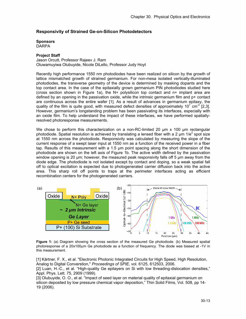
Responsivity of Strained Ge-on-Silicon Photodetectors Sponsors DARPA Project Staff Jason Orcutt, Professor Rajeev J. Ram Oluwamuyiwa Olubuyide, Nicole DiLello, Professor Judy Hoyt Recently high performance 1550 nm photodiodes have been realized on silicon by the growth of lattice mismatched growth of strained germanium. For non-mesa isolated vertically-illuminated photodiodes, the transverse geometry of the device is determined by masking dopants and the top contact area. In the case of the epitaxially grown germanium PIN photodiodes studied here (cross section shown in Figure 1a), the N+ polysilicon top contact and n+ implant area are defined by an opening in the passivation oxide, while the intrinsic germanium film and p+ contact are continuous across the entire wafer [1]. As a result of advances in germanium epitaxy, the quality of the film is quite good, with measured defect densities of approximately 107 cm-2 [2,3]. However, germanium’s longstanding problem has been passivating its interfaces, especially with an oxide film. To help understand the impact of these interfaces, we have performed spatially-resolved photoresponse measurements. We chose to perform this characterization on a non-RC-limited 20 µm x 100 µm rectangular photodiode. Spatial resolution is achieved by translating a lensed fiber with a 2 µm 1/e2 spot size at 1550 nm across the photodiode. Responsivity was calculated by measuring the slope of the current response of a swept laser input at 1550 nm as a function of the received power in a fiber tap. Results of this measurement with a 1.5 µm point spacing along the short dimension of the photodiode are shown on the left axis of Figure 1b. The active width defined by the passivation window opening is 20 µm; however, the measured peak responsivity falls off 5 µm away from the diode edge. The photodiode is not isolated except by contact and doping, so a weak spatial fall off to optical excitation is expected due to photogenerated carrier diffusion back into the active area. This sharp roll off points to traps at the perimeter interfaces acting as efficient recombination centers for the photogenerated carriers.
Figure 1: (a) Diagram showing the cross section of the measured Ge photodiode. (b) Measured spatial photoresponse of a 20x100μm Ge photodiode as a function of frequency. The diode was biased at -1V in this measurement. [1] Kärtner, F. X., et al. "Electronic Photonic Integrated Circuits for High Speed, High Resolution, Analog to Digital Converstion," Proceedings of SPIE, vol. 6125, 612503, 2006. [2] Luan, H.-C., et al. “High-quality Ge epilayers on Si with low threading-dislocation densities,” Appl. Phys. Lett. 75, 2909 (1999). [3] Olubuyide, O. O., et al. “Impact of seed layer on material quality of epitaxial germanium on silicon deposited by low pressure chemical vapor deposition,” Thin Solid Films, Vol. 508, pp 14-19 (2006).
(b)(a)

Chapter 30. Physical Optics and Electronics
30-14 RLE Progress Report 149
Low Power Thermo-optic Tuning of Microring Filters Sponsors DARPA Project Staff Reja Amatya, Professor Rajeev J. Ram Charles Holzwarth, Professor Henry I Smith Microring resonators have been used as tunable filters, wavelength switches, add-drop multiplexers, and modulators. Rings fabricated with HIC materials such as silicon dioxide claddings (n = 1.45), and silicon-rich silicon nitride (SiN) (n = 2.2) cores ensure tight beam confinement and low bending loss for most photonic applications. Compact size and compatibility with silicon integrated circuits (IC) make these ring resonators attractive for wavelength switching applications such as in electronic and photonic integrated circuits for signal processing and optical interconnects for supercomputer chips. With optimized heater design, we show low power thermal tuning for second-order SiN ring filters. Thermal tuning is necessary for postfabrication trimming. The effective (neff) and group (ng) refractive indices of the waveguide are temperature dependent. At 1.55μm, the thermo-optic coefficients (Δn/ΔT) for SiN and SiO2 are 4e-5 K-1 and 1.5e-5 K-1 respectively. For SiN rings with SiO2 cladding, the expected temperature tuning efficiency is 3.6GHz/K. Preliminary thermal tuning experiments on SiN rings with air cladding, using external heaters, show tuning of 4.5GHz/K. Figure 1 shows a comparison of experimental result with theory. The discrepancy is due to air cladding present in the test structure. We have designed and optimised heater structures for thermal tuning that ensure low tuning power. Thin titanium metal heaters (100nm) are fabricated on top of the cladding to locally change the temperature of the resonator. A finite-element thermal simulation (FEMLAB) was used to estimate the temperature profile of the waveguides with the heaters on top. The heater designs are optimized to give large temperature change for the rings with minimal input power, i.e. high thermal impedance (K/W). With the finalized heater design, the thermal impedance of 5,200 K/W is realized which suggest a tuning power of 52μW/GHz for the SiN rings. Figure 2 shows experimental and theoretical agreement between thermal impedance for the test heater. The predicted value for the optimized heater with simulation is shown to give low tuning power of 52μW/GHz.
Figure 2: Thermal impedance for test heater and optimized heater.
Figure 1: Thermal tuning range of 4.5GHz/K is achieved for second-order SiN resonator.