polymer composites with carbon nanotubes for printed electronics...
TRANSCRIPT
Polymer composites with carbon nanotubesfor printed electronics applications
Marcin Słoma, Warsaw University of Technology(27.02.2008, prof. Małgorzata Jakubowska, Warsaw University of Technology)
Abstract Nanomaterials are known for their superior
properties, and for that are the most investigated group of materials this days. These properties were utilized by the authors in new type of polymer thick film composition called „printed electronics”, that is a new trend in production of electronic devices. Printed electronics technology enables to manufacture low-cost electronic circuits using the well-known techniques such as screen printing, offset, or ink-jet, what is important in short production cycles or in fabrication of disposable electronics where cost of single circuit must be set to minimum. The use of nanostructures in the manufacture of the composition for printed electronics has opened new possibilities in the production of such structures. Paper presents achievements of the authors in the field of thick film composites containing carbon nanotubes development. Elaborated samples consists of poly(methyl methacrylates) and carbon nanotubes as a functional conductive phase. Screen printed polymer-nanotube layers demonstrated good electrical, optical, thermal and mechanical parameters, therefore idea of application of such structure was proposed. During three years of work, several applications of this materials were developed, such as transparent electrodes for electroluminescent structures, elastic thermistor on fabrics, pressure sensors, and low noise elastic resistors.
1. Introduction
Over the last decade there has been growing interest in the development of electronic components fabrication using printing techniques. Current studies are focused on adaptation of screen printing, ink-jet and roll-to-roll techniques for patterning electronics circuits and elaboration of new materials to obtain wide spectrum of properties. They represent potentially low-cost alternatives in production of flexible and disposable electronics, where stability of electrical properties under mechanical factors is required, or where silicon chip packaging cost are to high. Potential applications for
these circuits are flexible electronics [1], smart clothing [2] or biochemical sensors [3], or functional elements (i.e. printed transistors) [4,5].
Fast development of production and detailed analysis of properties of nanostructures, created new opportunities for production of printed electronics microcircuits. Nanomaterials, such as metal and ceramics nanopowders, carbon nanotubes (CNTs) or fullerenes, are now the most widely studied materials for this applications. Discovery and full characterization of carbon nanotubes, at the end of the last century [6], have created new opportunities in various fields of research and industrial sectors. The interest in nanotubes is due to their physical properties, unprecedented in other structures. Electrical and thermal conductivity of this structures, is one of the highest known today [7,8]. Also carbon nanotubes are the strongest and stiffest materials yet discovered [9]. Unusual properties were utilized in fabrication of various electronic and mechatronic structures, like resistors [10], biochemical sensors [11,12], field emission displays [13], diodes and transistors [14,15], memories [16], but also supercapacitors [17], artificial muscle fibers [18], composite construction materials [19] and hydrogen storage containers [20].
Main goal of the authors was to elaborate new type of materials based on polymer-nanotube composites, for screen printing deposition on various types of substrates, including elastic. Effective fabrication of such composites was possible with specially adapted methods of dispersion of nanotubes in polymer resins. This way authors obtained composite layers with new properties, directed for production with easy applicable, low cost and effective screen printing technique. Developed materials were successfully used in several applications, like elastic temperature sensors for textronic applications [21], resistive pressure sensors [22] and transparent electrodes for electroluminescent printed light sources [23], but also passive components like low noise polymer resistors [24].
437
XII International PhD WorkshopOWD 2010, 23–26 October 2010

2. Materials and preparation
Elaborated samples consists of poly(methyl methacrylate) (PMMA), organic solvent, and carbon nanotubes (CNTs) as a functional conductive phase. Components were homogenized to obtain thick film composition. Final samples were screen printed and thermally cured, to obtain composite layers
Materials used for printed electronics fabrication should be easy to obtain and low cost because of use in disposable and large-area structures. Therefore as-prepared multiwalled carbon nanotubes (MWCNTs) synthesized by catalytic chemical vapour deposition method (CCVD) were used. This method commonly used for large scale mass production of MWCNTs. Such material usually contains other carbon structures and residues of metal catalyst, what causes that purity of CNT load remain on low level (less than 95 %). On the other hand segregation and purification methods are expensive and can rise prices of CNTs more than dozen times. Morphology of used MWCNTs was evaluated under HRSEM (fig. 1), what allowed to characterise diameter and length to be 10-40 nm and 0.5-5 µm respectively, though longer structures were also observed.
F i g . 1 . P i c t u r e H R S E M o f u s e d c a r b o n n a n o t u b e s .
For synthesis of polymer resin, methyl methacrylate polymers and copolymers were used, and dissolved in organic solvents. Dissolving process was conducted with magnetic blade mixer for 48h in 40oC. Vehicle concentrations were selected with respect to rheology of compositions, and electrical properties of final composite layers.
To obtain final compositions, carbon nanotubes were dispersed in polymer resin. Electrical and optical properties were controlled by amount of CNTs in compositions in range from 0.1 wt.% to 5 wt.%. Nanotubes were added to selected resins, mixed in mortar, ultrasonically homogenized and finally three-roll-milled to break remaining CNT
agglomerates. Samples with macroscopically visible CNT agglomerates or areas with no CNTs were disqualified from further experiments.
Final layers were fabricated from compositions deposited on elastic polyester substrate by screen printing. Layers were cured in 130oC during 15 min to evaporate organic solvent. Additional silver11 contacts were also screen printed for resistance measurements. Figure 2 presents macroscopic picture of samples made from compositions containing 0.25 wt.% and 1 wt.% CNTs.
F i g . 2 . S c r e e n p r i n t e d a n d c u r e d c o m p o s i t i o n s w i t h 0 . 2 5 w t . % C N T ( l e f t ) a nd 1 w t . % CN T ( r i g h t ) .
3. Results and applications
Electrical properties of final layers were evaluated, after compositions printing and curing. Results of measurements showed relation between amount of CNTs in compositions and sheet resistance of obtained composite layers. All samples were electrically conductive, with resistance values ranging from 101 Ω/□ to 106 Ω/□ for layers made from compositions containing 5 wt.% to 0.1 wt.% of CNTs respectively. Moreover, layers with low amount of carbon nanotubes were optically transparent, with transmittance ranging from 19 % to 82 % for layers made from compositions containing 1 wt.% to 0.1 wt.% of CNTs respectively. Results of mechanical tests evaluation showed incomparable with other electronic structures properties. Resistance of composite layers remained stable during mechanical bending tests. Noticed resistance change was less than 10 % after 200 000 cycles of bending, while other materials such as transparent electrodes from ITO noted spike in resistance above 100 times. Polymer-graphite resistors compared in this test also changed resistance almost by 30 %. Similar test showed that polymer-nanotube layers are free from tensometric effect, that is common for polymer-graphite printed resistors. Thermal measurements showed that with proper control of CNT amount in layers we can obtain resistor with temperature coefficient of resistance close to stable polymer-graphite and metal-oxide fired resistors, but also resistors with high TCR in rage of 0.2 %/K, what provide opportunity to use this layers as temperature sensors.
438
Similar test, but conducted in low temperatures (5 K – 300 K) showed that measured low-tamperature TCR have similar values to today used cryostatic sensors based on ruthenium-oxide resistors. Results of noise level evaluations conducted during low-temperature resistance measurements showed, that level of 1/f type noise commonly occurring in resistors, is close to level of fired resistors, and way bellow noise level of polymer-graphite resistors. Detailed informations of conducted tests and results is provided below, with applications descriptions.
3.1 Transparent electrodes
Composite layers with controlled amount of CNTs, can be electrically conductive, yet optically transparent. Layers made from compositions containing 1 wt.% to 0.1 wt.% of nanotubes, were characterized by optical transmittance ranging from 19 % to 82 %. Resistance values of this layers was ranging from 103 Ω/□ to 106 Ω/□. Optimal amount of CNTs that enables to obtain low resistance with high transmittance was specified to be 0.25 wt.%. Layers obtained from this type of compositions have sheet resistance around 30 kΩ/□, and optical transmittance above 60 %. This values are inferior to those measured for sputtered ITO layers used as transparent electrodes, with sheet resistance form 102 Ω/□ to 104 Ω/□, and 70 % to 90 % of transmittance, but they superior this type of materials in stability of electrical properties under influence of mechanical stresses.
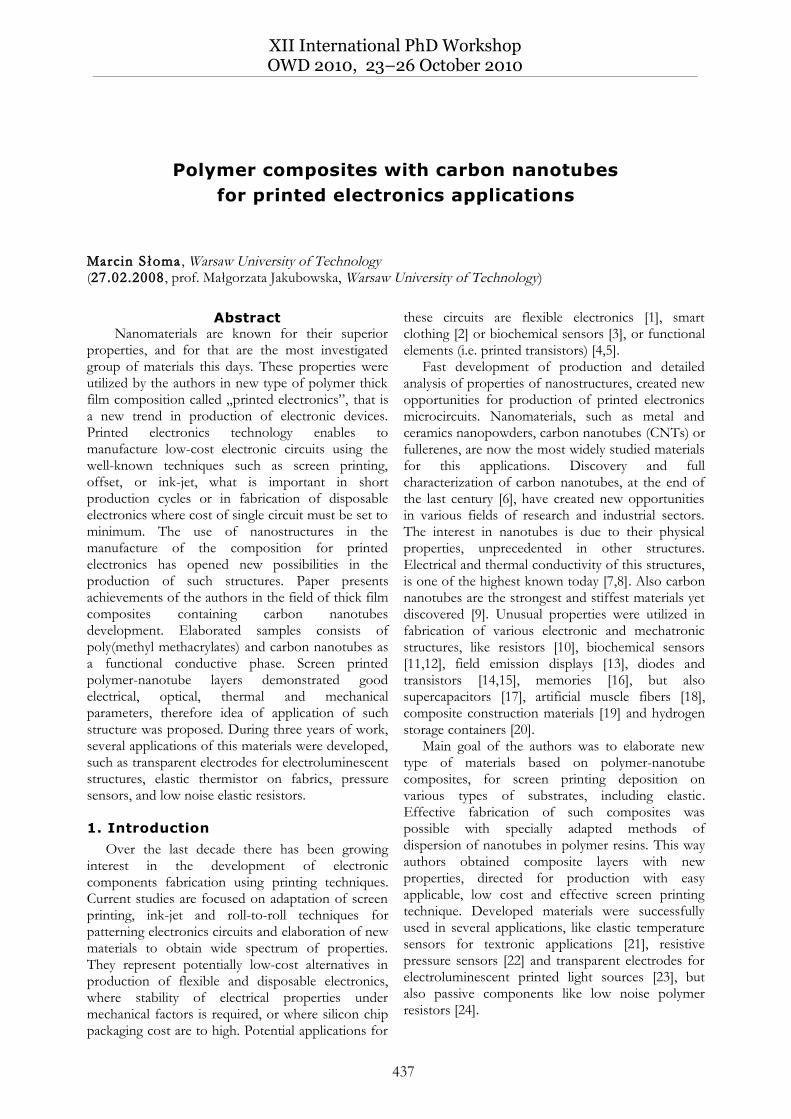
Both types of electrodes (polymer-nanotube and ITO) were subjected to periodical mechanical stresses. Test was performed on two types of polymer-nanotube layers (0.25 wt.%, 1 wt.%) and also on Acheson E421SS printed polymer-graphite nontransparent layers. Changes of resistance vs. number of cycles were investigated. Resistance values measured during bending cycles for all four samples are presented in figure 3.
F i g . 3 . V a l u e s o f s h e e t r e s i s t a n c e d u r i n g m e c ha n i c a l s t r e s s t e s t s .
Results showed that mechanical stresses negatively affected all tested samples. Electrical resistance increased after 200 000 cycles less than 10 % and around 3 % for layers printed from compositions containing 0.25 wt.% CNT and 1 wt.% CNT respectively. Polymer-graphite E421SS samples gained more than 27 % increase of resistance after the same number of cycles. On the other hand ITO samples gained almost three orders of magnitude increase of resistance. Last measurement of the ITO samples resistance was taken after 112 000 cycles, cause after around 120 000 cycles one of the ITO samples was destroyed.
This experiment clearly shows that mechanical stress have relatively low influence on polymer-nanotube layers. Nanotubes located in polymer base have very high length to diameter ratio, which prevents against contact loss between separate particles. Nanotubes have also high mechanical strength, and this kind of stress have no affect on their structure.
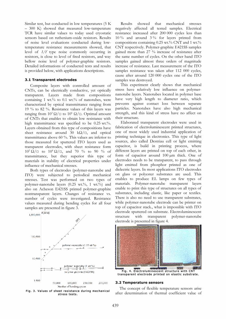
Elaborated transparent electrodes were used in fabrication of electroluminescent printed structures, one of most widely used industrial application of printing technique in electronics. This type of light sources, also called Destriau cell or light emitting capacitor, is build in printing process, where different layers are printed on top of each other, in form of capacitor around 100 µm thick. One of electrodes needs to be transparent, to pass through light emitted from phosphor printed as one of dielectric layers. In most applications ITO electrodes on glass or polyester substrates are used. This enables to produce EL lamps on few types of materials. Polymer-nanotube transparent layers enable to print this type of structures on all types of substrates, including elastic, like paper or textiles. There is also no need to use transparent substrates, while polymer-nanotube electrode can be printer on top of capacitor stack., what is impossible with ITO electrode sputtered on substrate. Electroluminescent structure with transparent polymer-nanotube electrode is presented in figure 4.
F i g . 4 . E l e c t r o l u m i n e s c e n t s t r u c t u r e w i t h C N T t r a n s p a r e n t e l e c t r o d e p r i n t e d o n e l a s t i c s u b s t r a t e .
3.2 Temperature sensors
The concept of flexible temperature sensors arise after determination of thermal coefficient value of
439

polymer-nanotube layers. Dependence of resistance characteristic on temperature change was observed for three sample types made of compositions with 0.25 wt.%, 1 wt.% and 5 wt.% CNTs, in temperature range from 20oC to 155oC. In the initial thermal cycle significant hysteresis was observed, therefore samples were cooled down and the measurements were repeated. Resistance change were negative in the full temperature range, from 4 % for 5 wt.% CNT samples to 19 % for 0.25 wt.% CNT samples. This type of resistance changes corresponds to -350 ppm/K and -2100 ppm/K respectively. Values or resistance change and corresponding TCR are summarized in table 1.
T a b . 1 .
T i t l e o f t a b l e
Sample ΔR|20°C – 155°C [%] TCR [ppm/K]0.25 wt.% CNT 19 -2100
1 wt.% CNT 10 -8005 wt.% CNT 4 -350
From compositions containing 1 wt.% and 0.25 wt.% of nanotubes, elastic temperature sensors on fibers were fabricated. Sensors were made with dip-coating method, but this materials can be screen printed on textiles as well. Values of TCR, along with resistance from 103 Ω/□ to 105 Ω/□, provide measurement accuracy up to 0.1°C, what enabled to utilize this type of sensors for human body temperature monitoring in smart clothing, and textronic applications. Temperature sensor on fiber fabricated from polymer-nanotube composition is presented in figure 5.
F i g . 5 . E l a s t i c t e m p e r a t u r e s e n s o r o n f i b e r f a b r i c a t e d f r o m p o l y m e r - n a n o t u b e c o m p o s i t i o n .
Unfortunately polymer paste application in elastic electronics is causing serious problem connected with tensometric effect. Mechanical stresses connected with stretching or bending of elastic polymer resistors can introduce dramatic resistance change, reaching few times of the initial value. This phenomenon is caused by influence of conductive particles position change within elastic sensor
structure and depended directly on the elongation of the sensor body. Similar sensors fabricated earlier from polymer-graphite compositions exhibited strong tensometric effect, that resulted in 60 % change in resistance under bending test. Therefore another experiment was performed, focused on resistance stability during curvature change of the polymer-nanotube samples. Resistance changes in function of bending radius are presented in figure 6.
F i g . 6 . V a l u e s o f s h e e t r e s i s t a n c e d u r i n g b e n d i n g t e s t .
Significant property of elaborated polymer-nanotube sensors is lack of tensometric effect. Under constant mechanical tension, as well as under dynamic test, layers didn’t change they resistivity. This feature is critical for most elastic electronic applications, including textronics and elastic circuics.
3.3 Cryostatic sensors
Temperature dependencies of resistance was also measured in cryostat in temperature range from 5 K up to 300 K. While temperature in cryostat was slowly rising, samples resistance and temperature were recorded continuously. In studied temperature range TCR changes its value from -680 ppm/K at T = 300 K to -0.162 K-1 at T = 5 K. Dimensionless sensitivity parameter, that is usually calculated for cryogenic temperature sensor, is almost the same as for ruthenium cryogenic sensors with calculated values in the range from 0.18 to 0.88. Sensors printed on elastic substrates can be used for precise measurements of surface temperature, even for objects with complex shapes. Currently used thick film resistive sensors are placed stationary in cryostatic chamber what usually creates differences in temperature measurements, or need for long time stabilization of temperature in whole volume of cryostat.
3.4 Pressure sensors
For fabrication of pressure sensors, contact resistance fluctuation effect was used. Resistance fluctuation observed on contact of two conducting surfaces is crucial parameter for application in pressure sensors or surface potentiometers. This effect is well known in polymer-carbon layers applications, described as decrees of resistance with applied increasing pressure. Contact resistance is decreasing with linear characteristic in logarithmic
440
coordinates. Printing techniques used for fabrication of this sensors allows to create various two dimensional shapes, tailored to measured surfaces.
In this case resistive layers were printed as two round shapes of 5 mm diameter with additional polymer-silver conductive measurement contacts. Sensors were fabricated from compositions containing 0.1 wt.%, 0.25 wt.% and 0.5 wt.% of CNTs, cured in 130°C for 30 min. Polyester PET films were used for substrates. Printed structure was creased half way between two resistive circles, to provide best contact between them. Low nanotube content in the layers provide low probability of electrical contact between two layers, but under increasing pressure this probability rises very fast. In this experiment more than 1500 times increase of contact resistance was noted under provided force from 40 g to 400 g. This is way above resistance changes measured for other carbonic filling material such as fine grained graphite or carbon black, that noted at most 100 times increase of contact resistance. Furthermore, because of low CNT loading, all fabricated layers were optically transparent with transmittance in range from 40% to 82 %. This allows to produce new type of elastic and transparent pressure sensors. Also high resistance to mechanical stresses and lack of tensometric effect, allows to create more sensitive sensors, with higher endurance to mechanical factors.
3.5 Elastic resistors
Summarizing all above application we will notice that all properties mentioned in this paper characterize polymer resistors. With resistance ranging from 101 Ω/□ to 106 Ω/□ it is possible to obtain wide range of printed resistors. We can even produce transparent resistors, it there is need for that application. Resistance to mechanical stresses, and lack of tensometric effect lead to elastic resistor application, on polymer films, paper or even textiles. Low value of TCR (350 ppm/K) is sufficient for medium reliability applications.
During measurements of temperature dependencies of resistance in temperatures from 5 K up to 300 K., also noise identification and noise level measurements were taken. Noise level is also important parameter in terms of material application, for electronic elements, in particular for production of resistors. Noise spectra shape and their dependence on excitation voltage were tested to identify the noise. Power spectral densities of voltage fluctuations, initially measured in room temperature for several bias voltages indicated that the noise observed in studied samples in room temperature is resistance 1/f noise. Noise intensity calculated from low-frequency noise spectroscopy (LFNS) measurements, allowed to identify thermally activated noise sources (TANS), and calculate their
value to be 24.6 meV for 15 K – 25 K temperatures, and 0.67 eV – 1.6 eV for 80 K – 300 K temperatures. Observed values of activation energies of TANS are similar to these observed in thick film metal-oxide resistors. Bulk noise intensity calculated for polymer-nanotube resistors with value of Cbulk = 1.28∙10-22 m3 is close to the value 2∙10-22 m3 for RoHS RuO2 layers, however it is still an order of magnitude larger than 10-23 m3 obtained for lead-containing RuO2 based resistors, withdrawn form commercial applications. In comparison, Cbulk
values of polymer-graphite resistors are almost two orders higher (Cbulk≈ 3∙10-20 m3) than calculated for elaborated resistors. This again indicates possibility of application polymer-nanotube composites in printed electronics technology.
4. Summary
Discovery of nanomaterials opened new possibilities in production field of printed electronics. In this paper authors are presenting new types of sensors, transparent electrodes and other electronic applications, intended for apply with screen printing technique on various substrates including elastic foils, paper and textiles. Polymer-nanotube electrodes and resistors elaborated by the author, present interesting electrical and mechanical properties. Transparent electrodes overcome today used ITO layers, with resistance to mechanical stresses, and allows to fabricate elastic electroluminescent structures on any type of substrate, not only transparent ones. Elastic temperature sensors in form of printed elastic stripes or dip coated fibbers present high elasticity, very high TCR and lack of tensometric effect, what make them suitable for production of textronics and smart clothing. In cryostatic temperatures resistive layers shows stable and repeatable resistance changes during cooling and heating. Initial elasticity in room temperature allows to use them as cryostatic temperature sensors mounted directly on objects, even with complex geometry. Printed pressure sensors are easy to produce, can have shapes fitted to measured surface and outperform similar sensors based on graphite or carbon black powders. Parameters essential for applications in electronics measured for polymer-nanotube resistors, correspond to those obtained for other carbon composites and fired metal-oxide resistors, or even exceed them in the case of carbon filled resistors. Presented results are part of work directed to fabrication of group of composites filled with nanomaterials, for printed electronics application.
This work was supported through MNiSW Grant No. N N515 081437 in years 2009-2010, and also financed from MNiSW funds for science in the years 2009-2010 as research project.
441

5. Bibliography
[1] Sirringhaus, H. et al., High-Resolution Inkjet Printing of All-Polymer Transistor Circuits, 2000, Science 15, vol. 290, pp. 2123 – 2126.
[2] Axisa F, Dittmar A., Delhomme G., Smart clothes for the monitoring in real time and conditions of physiological, emotional and sensorial reactions of human, Proceedings of the 25th Annual International Conference of the IEEE, 2004, vol. 4, pp. 3744-3747.
[3] Erdema A., et al., Electrochemical genomagnetic assay for the detection of hepatitis B virus DNA in polymerase chain reaction amplicons by using disposable sensor technology, Electrochemistry Communications, 2005, vol. 7, pp 815-820.
[4] Hines D. R., Mezhenny S., Breban M., Williams E. D., Nanotransfer printing of organic and carbon nanotube thin-film transistors on plastic substrates, 2005, Appl. Phys. Lett. 86.
[5] Cao Q., Zhu Z-T., et al., Transparent flexible organic thin-film transistors that use printed single-walled carbon nanotube electrodes, 2006, Appl. Phys. Lett. 88.
[6] Iijima S., Helical microtubules of graphitic carbon, 1991, Nature vol. 354, pp. 56-58.
[7] Dresselhaus M., Dresselhaus G., Avouris P., Carbon Nanotubes: Synthesis, Structure Properties and Applications, 2001, Springer-Verlag, Berlin
[8] Saito R., Dresselhaus G., Dresselhaus M.S.: Physical properties of carbon nanotubes, Imperial College Press, 1998
[9] Min-Feng Y., et al, Strength and Breaking Mechanism of Multiwalled Carbon Nanotubes Under Tensile Load, 2008, Science 287, pp. 637–640.
[10] Hsu W. K., et al., Circuit elements in carbon nanotube-polymer composites, 2004, Carbon 42, p. 1707.
[11] Tran T.H., Kwon J.H., Lee K.S., Lee J.W., Ju B.K., pH Sensor Using Carbon Nanotubes as Sensing Material, 2006, First International Conference on Communications and Electronics, 2006. ICCE '06., pp. 490 – 493
[12] Pham A., Carbon Nanotube Resonator Sensors for Remote Sensing Systems, IEEE Topical Conference on Wireless Communication Technology, 2003.
[13] Zhao, W.J.; Wasu, R.; Takai, M., Field emission from carbon nanotube mat, 2003, Technical Digest of the 16th International Vacuum Microelectronics Conference, p. 57 – 58
[14] Zhen Yao, Henk W. Ch. Postma, Leon Balents,Cees Dekker, Carbon nanotube
intramolecular junctions, Nature 402, 273-276 (18 November 1999)
[15] Tans S. J., Verschueren A., Dekker C., Room-temperature transistor based on a single carbon nanotube, 1998, Nature 393, 49-52.
[16] Rueckes T., et al, Carbon Nanotube-Based Nonvolatile Random Access Memory for Molecular Computing, 2000, Science Vol. 289. no. 5476, pp. 94 – 97.
[17] Jurewicz K. et al., Supercapacitors from nanotubes/polypyrrole composites, 2001, Chem. Phys. Lett., 347, 36–40.
[18] Baughman R. H. et al., Carbon Nanotube Actuators, 1999, Science Vol. 284, no. 5418, pp. 1340 – 1344
[19] Boccaccini A. R., Acevedo D. R., Brusatin G., Colombo P., Borosilicate glass matrix composites containing multi-wall carbon nanotubes, 2005, Journal of the European Ceramic Society 25, pp.. 1515-1523.
[20] Zidan R., Rao A. M., Doped Carbon Nanotubes for Hydrogen Storage, 2002, U.S. DOE Hydrogen Program Review.
[21] Sibiński M., Jakubowska M. Słoma M., Flexible Temperature Sensors on Fibers, Sensors 2010, 10(9), 7934-7946.
[22] Jakubowska M., Łukasik M., Młożniak A., Słoma M., Contact resistance of polymer thick films filled with carbon nanotubes, 2008, Materiały Elektroniczne Nr 3, pp. 92-100
[23] Ptak J., Cież M., Zaraska K., Jakubowska M., Słoma M., A comparison of electrooptical characteristics of the electroluminescent lamps with transparent electrodes based on ITO and CNT, 2009, Large-area, Organic & Printed Electronics Convention, Frankfurt
[24] Stadler A. W., Kolek A., Mleczko K., Zawiślak Z., Ptak P., Jakubowska M., Słoma M., Właściwości elektryczne grubowarstwowych rezystorów na bazie kompozycji polimerowych z nanorurkami węglowymi, IX Krajowa Konferencja Elektroniki 2010, Darłówko Wschodnie
Authors:
MSc. Eng. Marcin Słoma Warsaw University of Technology Faculty of Mechatronics ul. św. A. Boboli 8 02-525 Warszawa tel. (022) 234 84 80 fax (022) 848 37 64
email: [email protected]
442