power electronic building block network simulation testbed
TRANSCRIPT

N PS ARCHIVE1997.06BADORF, M.
NAVAL POSTGRADUATE SCHOOLMONTEREY, CALIFORNIA
THESIS
POWER ELECTRONIC BUILDING BLOCKNETWORK SIMULATION TESTBED
STABILITY CRITERIA AND HARDWAREVALIDATION STUDIES
by
Michael G. Badorf
June, 1997
ThesisB1250124
Thesis Advisor: Robert W. Ashton
Approved for public release; distribution is unlimited.


REPORT DOCUMENTATION PAGE Form Approved OMB No. 0704-01 i
Public reporting burden for this collection of information is estimated to average 1 hour per response, including the time for reviewing instruction, searching existing data
sources, gathering and maintaining the data needed, and completing and reviewing the collection of information. Send comments regarding this burden estimate or any other
aspect of this collection of information, including suggestions for reducing this burden, to Washington Headquarters Services, Directorate for Information Operations and
Reports, 1215 Jefferson Davis Highway, Suite 1204, Arlington, VA 22202^4302, and to the Office of Management and Budget, Paperwork Reduction Project (0704-0188)
Washington DC 20503.
1 . AGENCY USE ONLY (Leave blank) REPORT DATEJune 1997
3 . REPORT TYPE AND DATES COVEREDMaster's Thesis
4. TITLE AND SUBTITLEPOWER ELECTRONIC BUILDING BLOCK NETWORK SIMULATION TESTBEDSTABILITY CRITERIA AND HARDWARE VALIDATION STUDIES
6. AUTHOR(S) Michael G. Badorf
5. FUNDING NUMBERS
7. PERFORMING ORGANIZATION NAME(S) AND ADDRESS(ES)
Naval Postgraduate School
Monterey CA 93943-5000
8. PERFORMINGORGANIZATIONREPORT NUMBER
SPONSORING/MONITORING AGENCY NAME(S) AND ADDRESS(ES) 10. SPONSORING/MONITORINGAGENCY REPORT NUMBER
11. SUPPLEMENTARY NOTES The views expressed in this thesis are those of the author and do not reflect the
official policy or position of the Department of Defense or the U.S. Government.
12a. DISTRIBUTION/AVAILABILITY STATEMENTApproved for public release; distribution is unlimited.
12b. DISTRIBUTION CODE
13. ABSTRACT (maximum 200 words)
Naval power distribution has principally used an AC network to supply loads. With the advent
of new power electronic devices, the focus has shifted to employing a DC distribution system that
eliminates large transformers and mechanical switching devices and enhances the survivability of the
platform. The Power Electronic Building Block (PEBB) Network Simulation Testbed currently under
construction at the Naval Postgraduate School is a study into the feasibility of such DC systems.
The objective of this thesis was to perform theoretical and simulation-based analysis to
establish quantitative criteria for PEBB Testbed stability. These criteria were then used to develop a
set of hardware studies to investigate the interaction of components within the PEBB Testbed. Finally,
the hardware studies were utilized to verify PEBB Testbed performance.
Principal conclusions of this research included that the PEBB Testbed demonstrated stability
under all simulated loading conditions. Follow-on testing of the PEBB Testbed confirmed that the
simulations correlated well with hardware implementation. In addition, the hardware validation
studies revealed that switching harmonics had a considerable effect on the system output.
14. SUBJECT TERMS buck converters, dc-to-dc converters, power electronic building
blocks, control of power converters, parallel dc-to-dc converter operation
15. NUMBER OFPAGES 162
16. PRICE CODE
17. SECURITY CLASSIFICA-
TION OF REPORTUnclassified
18. SECURITY CLASSIFI-
CATION OF THIS PAGEUnclassified
19. SECURITY CLASSIFICA-
TION OF ABSTRACTUnclassified
20. LIMITATION OFABSTRACTUL
NSN 7540-01-280-5500 Standard Form 298 (Rev. 2-89)
Prescribed by ANSI Std. 239-18 298-102

11

Approved for public release; distribution is unlimited.
POWER ELECTRONIC BUILDING BLOCK NETWORK SIMULATIONTESTBED STABILITY CRITERIA AND HARDWARE VALIDATION STUDIES
Michael G. Badorf
Lieutenant, United States Navy
B.S., United States Naval Academy, 1990
Submitted in partial fulfillment
of the requirements for the degree of
MASTER OF SCIENCE IN ELECTRICAL ENGINEERING
from the
NAVAL POSTGRADUATE SCHOOLJune 1997


ABSTRACT
Naval power distribution has principally used an AC network to supply loads.
With the advent ofnew power electronic devices, the focus has shifted to employing a
DC distribution system that eliminates large transformers and mechanical switching
devices and enhances the survivability of the platform. The Power Electronic Building
Block (PEBB) Network Simulation Testbed currently under construction at the Naval
Postgraduate School is a study into the feasibility of such DC systems.
The objective of this thesis was to perform theoretical and simulation-based
analysis to establish quantitative criteria for PEBB Testbed stability. These criteria were
then used to develop a set of hardware studies to investigate the interaction of
components within the PEBB Testbed. Finally, the hardware studies were utilized to
verify PEBB Testbed performance.
Principal conclusions of this research included that the PEBB Testbed
demonstrated stability under all simulated loading conditions. Follow-on testing of the
PEBB Testbed confirmed thatthe simulations correlated well with hardware
implementation. In addition, the hardware validation studies revealed that switching
harmonics had a considerable effect on the system output.

VI

TABLE OF CONTENTS
I. INTRODUCTION 1
II. POWER SECTION DESIGN 5
A. TOPOLOGY 5
B. SPECIFICATIONS AND COMPONENT SELECTION 6
1. Switch and Diode Selection 7
2. Output Inductor Sizing and Switching Frequency 8
3. Output Capacitor Sizing 10
4. Input Filter Sizing 11
C. SUMMARY 12
III. CONTROL ALGORITHM DEVELOPMENT 13
A. OPEN-LOOP ABCD STATE SPACE MODEL 13
B.KASSAKIAN ALGORITHM 15
C. STATE DIFFERENCE IMPLEMENTATION IN HARDWARE 16
1. Basic Implementation 16
2. Feedforward Gain 17
3. Source Buck Converter House Curve 19
D. SUMMARY 20
IV. CONTROLLER GAIN SELECTION 23
A. ANALOG CONTROLLER GAIN SELECTION 23
1. Computer Modeling 23
2. Source Buck Converter Transient Specifications 24
3. Closed Loop Model 24
4. Pole Placement And Gain Selection 25
5. Effect of Output Capacitor Sizing 29
B. DIGITAL CONTROLLER GAIN SELECTION 31
1. Computer Modeling 31
2. Pole Placement and Gain Selection 31
3. Summary of Digital Controller Gain Selections 32
C. SUMMARY 33
V. SIMULATION AND HARDWARE RESULTS 35
A. BACKGROUND 35
B. MODE 1 OPERATION 36
C. MODE 2 OPERATION 37
D. MODE 3 OPERATION 42
E. MODE 4 OPERATION 43
F. MODE 5 OPERATION 47
G. MODE 6 OPERATION 52
H. MODE 7 OPERATION 55
I. SUMMARY 58
vii

VI. SCHEMATICS 59
A. CIRCUIT BOARD BACKGROUND 59
1. Easytrax Overview 59
2. Circuit Labeling 59
B. CIRCUIT DIAGRAMS AND DESCRIPTIONS 61
1. Source and Load Buck Converter Topologies 61
2. Sensor Board 63
3. Analog Control Board 63
4. IGBT Driver Board 73
5. Digital Control Board 74
VII. CONCLUSIONS 75
APPENDIX A. DATA SHEETS 79
A. INTERNATIONAL RECTIFIER IRGT1090U06 IGBT 79
B. UNITRODE UC3637 PWM DRIVER IC 85
APPENDIX B. SIMULINK BLOCK DIAGRAMS AND MATLAB CODE 93
A. SOURCE BUCK CONVERTER 93
1. Matlab M-file buckcons.m 93
2. Matlab M-file buckstrt.m 95
3. Matlab M-file buckfull.m 97
4. Matlab M-file buckten.m 98
5. Matlab M-file buckplot.m 99
6. Simulink Block Diagram 100
B. LOAD BUCK CONVERTER 101
1. Matlab M-file buckcons.m 101
2. Simulink Block Diagram 103
APPENDIX C. ACSLCODE 105
A. SOURCE BUCK CONVERTER GAIN SELECTION CODE 105
1. Main Program 105
2. Buck Converter Macro 107
3. Analog Controller Macro 109
4. Command File 110
B. LOAD BUCK CONVERTER GAIN SELECTION CODE 112
1. Main Program 112
2. Command File 116
C. MODE 7 DETAILED SIMULATION CODE 118
1. Main Program 118
2. Buck Converter Macro 128
3. Source Buck Converter Input Filter Macro 130
4. Load Buck Converter Input Filter Macro 131
5. Command File 132
Vlll

APPENDIX D. EASYTRAX PCB DATA 137
A. ANALOG CONTROLLER PCB DATA 137
1. Component List 137
2. Net List 139
3. PCB Component Overlay 141
B. PHASE-LOCKED LOOP PCB DATA 142
1. Component List 142
2. Net List 142
3. PCB Component Overlay 143
C. IGBT DRIVER CIRCUIT PCB DATA 144
1. Component List 144
2. Net List 144
3. PCB Component Overlay 145
D. SENSOR BOARD PCB DATA 146
1. Component List 146
2. Net List 147
3. PCB Component Overlay 148
LIST OF REFERENCES 149
INITIAL DISTRIBUTION LIST 151
IX


I. INTRODUCTION
Naval power distribution has principally used AC networks to supply loads. With
the advent of new power electronic devices, the focus has shifted to employing a DC
distribution system that eliminates large transformers and mechanical switching devices
and enhances the survivability of the platform. The Power Electronic Building Block
(PEBB) Network Simulation Testbed currently under construction at the Naval
Postgraduate School will be used to study the feasibility of such DC systems.
The proposed architecture for this shipboard power distribution scheme is shown
in Figure (1-1). In this distribution network the main feeders are DC. The ship is
C >TVGEN2 AC DC
PORT DC BUS
iZSSCM
RECTIFIER DC
:> DCLOADS
ZONE DCAUCTIONEER
lZSSCM—?\—
RECTIFIER
* 3E
7V
DC
GEN 1
^>a£DC
DC
<z.
SSUVI
SSCM~7T~
ACLOADS
CIz
STBD DC BUS
>
Figure 1-1, Integrated Power System (from [Ref. 1])

divided into zones with each zone containing common energy conversion devices fed
from the DC busses. The DC power is distributed via port and starboard busses from the
source(s) into the separate zones. Each zone contains a number of Ship Service
Converter (SSCM) and Inverter Modules (SSIM). The SSCM is used in each zone to
step-down the distribution bus voltage to a regulated level for use in the zone. In this
way the SSCM inserts intelligence into the system by acting to buffer, preregulate and
fault protect each zone. Electric loads within the zone are fed by either SSCMs or SSIMs
depending on the load's requirement for DC or AC power.
The focus of this thesis is on the design of SSCMs and their subsequent
integration with SSIMs in a DC distribution network. Coincident to this research is the
development of system stability criteria. As a result, theoretical and simulation-based
analysis will be performed to establish quantitative criteria for system stability. These
criteria will then be used to develop a set of hardware studies to investigate the
interaction of components within the PEBB Network Simulation Testbed. Finally, the
hardware studies will be conducted to verify system performance.
The documentation detailing this research is organized into six chapters. In
Chapter II, the basic design of the SSCM power section is presented. Chapter III deals
with the development of SSCM analog and digital closed-loop state-difference control
algorithms. Pole placement and gain selection for these controllers are investigated in
Chapter IV. With the SSCM gains determined, detailed simulations of integrated
SSCM/SSIM operations are documented in Chapter V. This chapter also includes
hardware study results for some of the simulation configurations studied.

Circuit operations and schematics for the SSCM power section and controller are covered
in Chapter VI. The final chapter contains a summary of the research work, notable
conclusions and recommendations for future work.


II. POWER SECTION DESIGN
A. TOPOLOGY
This project focused on the design, implementation and testing of high-bandwidth
DC-to-DC buck converters. Figure (2-1) illustrates the basic circuit topology.
Figure 2-1, DC-To-DC Buck Converter Topology
Following a full development in reference [2], it can be shown that the buck converter
acts as a DC step-down transformer. The reduction in voltage is governed by the duty
cycle of the switch according to
VC =DE (2-1)
where D is the duty cycle. From Equation (2-1), it is evident that any desired output
voltage can be attained by controlling the duty cycle.
System design called for the application of this topology as part of the DC Zonal
Electrical Distribution (DC ZED) Network envisioned for the Surface Combatant for the
twenty-first century. As part of the basic research into DC ZED, a Power Electronic
Building Block (PEBB) Network Simulation Testbed is being assembled at the Naval

Postgraduate School. A general topology of this network is pictured in Figure (2-2).
From the diagram, it can be seen that two Source Buck Converters condition rectified
three-phase power and provide the network with regulated DC power. This power is
directed to loads supplied by two Load Buck Converters and four Auxiliary Resonant
Commutated Pole (ARCP) Inverters.
3 Phase ACPower Supply
Terminal
Block
AC Circuit
Breaker3 Phase
Rectifier
Source
Buck#lSource
Buck #2
ARCP#1 ARCP #2 ARCP #3 ARCPM LoadBuck#l Load Buck #2
Load#l Load #2 Load #3 Load #4 Load #5 Loadm
Figure 2-2, DC Distribution System
Specifications for the Source and Load Buck Converters are given below. Detailed
design descriptions of the ARCP units are given in reference [3].
B. SPECIFICATIONS AND COMPONENT SELECTION
Minimum design specifications for the Source and Load Buck Converters were
provided by the Naval Surface Warfare Center, Carderock Division/Annapolis
Detachment. Table (2-1) summarizes the requirements. Using this information,

component sizing and selection was performed. The final results of this analysis are
documented in Table (2-2). Analysis of each component selection is given below.
Parameter Source Buck Load Buck
Maximum Output Power 9kW 3kW
Switching Frequency 5-25 kHz Hard Switched 5-25 kHz Hard Switched
Input (nominal) 400 VDC / 22.5 A 300VDC /10A
Output (nominal) 300 VDC / 30 A 208VDC /14.5A
Continuous Operations 10% to 100% Loading 10%> to 100% Loading
Table 2-1, Buck Converter Specifications
Component/Parameter Source Buck Load Buck
Switch / Diode International Rectifier
IRGT1090U06 600V/90A
IGBT Power Modules
International Rectifier
IRGT1090U06 600V/90A
IGBT Power Modules
Input Filter Capacitor Sprague Powerlytic
2000 uF, 450 VDC
Two Sprague Powerlytic
230 uF, 450 VDC, Paralleled
Input Filter Inductor 0.425 mH, hand wound 0.425 mH, hand wound
Output Capacitor Sprague Powerlytic
400 uF, 450 VDC
Sprague Powerlytic
400 uF, 450 VDC
Output Inductor 0.760 mH, hand wound
0.875 mH, hand wound
1 .3 mH, hand wound
Switching Frequency 20 kHz 20 kHz
Output Voltage Ripple <1% <1%
Table 2-2, Component Selection Results
1. Switch and Diode Selection
For both the Source and Load Buck Converters, International Rectifier 600V/90A
IGBT Power Modules were chosen based on their high current density, rugged design,
and simple gate drive. In addition, the INT-A-pak "half-bridge" packaging lends itself to
the buck converter topology. One power module contains two IGBT / diode pairs
allowing co-location of the switch and diode components. Appendix (A) contains the
data sheet for this component.
2. Output Inductor Sizing and Switching Frequency
a. Source Buck Converter
Inductor sizing was done to maintain continuous inductor current over a
load range of 10% -» 100%. Based on this range, the most limiting condition for
continuous inductor current occurs at minimum load. To maintain continuous operations
at this point, the inductor must be wound to meet or exceed the critical inductance for the
circuit. This value is given in reference [2] by
Lcri« = ™-(1-D) (2-2)
where T is the switching period and R is the resistance at minimum loading.
Analysis of Equation (2-2) shows that two of the input parameters are set.
From Equation (2-1), the duty cycle is 75%. In addition, load resistance is 100 Q based
on a nominal output voltage of 300 V. As a result, only the switching period, or
conversely the switching frequency, must be set. Utilizing Table (2-1), the switching
frequency was chosen to be 20 kHz. This selection corresponds to a switching period of
50 usee and provides the following advantages:
• minimization of required inductor size
E-V• minimization of the inductor ripple current given by A / = — • DT
Is
• elimination of audible switching noise of the buck converter

• maintains a 5 kHz margin to the maximum hard-switched limit of the IGBTs.
Substituting into Equation (2-2), critical inductance was found to be 625 uH. The actual
inductances achieved for the two Source Buck Converters were 760 uH and 875 uH
respectively.
This sizing was not made any larger than necessary because of the tradeoff
between desired inductance and the size required to achieve that inductance. At full load,
inductor current has a 30 A dc offset. This dc component drives a single, wound inductor
core sized to Lcrit
into saturation. As a result, each inductor was made from several cores
wound in series. Cores were wound to minimize saturation effects while maximizing
inductance per core. The overall inductance is then given by summing each of the series
core inductances. Reference [4] contains core sizing information.
b. Load Buck Converter
Inductor sizing was done to maintain continuous inductor current over a
load range of 10% -> 100%. A 20 kHz switching frequency was chosen for the reasons
mentioned above. Substituting appropriate values into Equation (2-2) yielded a critical
inductance of 1 . 1 mH. In actuality, a 1 .3 mH inductance value was achieved for each
Load Buck Converter. Contrary to the Source Buck Converters, core saturation due to dc
offset was not a concern since the maximum load current is well below saturation levels.
As a result each inductor was wound using one core thus saving space in the Load Buck
Converter topology.

3. Output Capacitor Sizing
a. Source Buck Converter
Capacitor selection was based on maintaining less than 1% voltage ripple
on the Source Buck Converter output. From reference [2], percent voltage ripple is
given by:
AVC
T2 (l-D)
Substituting the appropriate values, the minimum output capacitance is found to be
10 uF. Based on this small size, rapid transient response can be expected. Computer
simulation and gain selection detailed in Chapter IV, however, shows that the transient
voltage response is unacceptably soft at such low output capacitance values. Utilizing
these results, 400 uF Sprague electrolytic capacitors were selected. This choice provided
the required transient response and built in a design margin for testing above the 10% ->
100% —> 10%) load transient used for analysis in Chapter IV.
b. Load Buck Converter
Capacitor selection was based on maintaining less than 1% voltage ripple
on the Load Buck Converter output. Utilizing Equation (2-3), minimum output
capacitance was determined to be 7.5 uF. Using computer simulation and gain selection
results detailed in Chapter IV, 400 uF Sprague electrolytic capacitors were selected to
provide the required voltage transient response.
10

4. Input Filter Sizing
a. Source Buck Converter
One circuit element not shown in the basic buck converter topology of
Figure (2-1) is the input LC lowpass filter. The input filter is documented in Figure (6-1)
of Chapter VI. Initial filter design focused on component selection to provide 10 dB of
attenuation at 60 Hz. Component sizing and dc attenuation concerns, however, make this
design impractical. As a result, ac ripple rejection analysis shifted to a combined
filter/controller loop speed method. In this arrangement, the input LC filter decouples the
rectifier source from the Source Buck Converter input by at least 10 dB of attenuation for
frequencies 360 Hz and above. The controller loop speed of the Source Buck Converter
is then tasked with providing ac ripple rejection below 360 Hz. Chapter IV contains a
discussion on controller loop speed.
Central to the selection of capacitor and inductor values was the placement
of the resonant peak of the input LC filter. The resonance acts to amplify low frequency
components in the supply voltage. As a result, peak placement must minimize this
amplification for the frequencies of concern. Since the supply voltage is rectified 3-phase
power, these frequencies are 60 Hz, 120 Hz, and 360 Hz. Matlab analysis revealed that a
resonant peak placed at 1 80 Hz provides the desired response. This value was obtained
using a capacitance of 2000 uF and an inductance of 391 uH. In actuality, a 173 Hz
resonant peak was achieved using a 2000 uF capacitor and 425 uH inductor.
11

b. Load Buck Converter
The input filter to the Load Buck Converters was designed to provide
decoupling from the output of the Source Buck Converters. As a result, the LC
combination had to be chosen to place the resonant peak of the Load Buck Converter
input filter below the slowest controller poles of the Source Buck Converters. Based on
the pole placement/gain selections detailed in Chapter IV, the resonant peak of the input
LC filter was set at 360 Hz using a capacitance of460 uF and an inductance of 425 fiH.
C. SUMMARY
With the basic power sections of the Source and Load Buck Converters
established, the design effort focused on the development and implementation of an
appropriate control scheme. As will be shown in Chapter III, open-loop operations of a
buck converter are extremely underdamped under transient conditions. Therefore,
satisfactory system transient response must be obtained by "closing the loop". Once the
required control algorithm has been established, gain selections and simulations can be
performed to produce stability criteria for hardware testing.
12

III. CONTROL ALGORITHM DEVELOPMENT
A. OPEN-LOOP ABCD STATE SPACE MODEL
The first step in controller development required the determination of the open-
loop state space equations. In state space analysis, energy storage devices dictate the
state variables. Referring to Figure (2-1) in Chapter II, the obvious state variable choices
are capacitor voltage and inductor current. With the switch shut, the state equations are:
dvc
dt C h~ R(3-1)
dh Ire l—- = —\E-vr \
dt L V CJ (3-2)
With the switch open, the state equations become:
dvc 1
dt C
dlL 1 r
dt" L [
0-vc ]
(3-3)
(3-4)
Combining like equations into an averaged model yields
dvcdt C R
(3-5)
^ = hdE-vc ]dt L [ CJ (3-6)
where the duty cycle, d, is given by:
d = switch on
+ t Tswitch on switch off switch
(3-7)
13

with Tswitch= switching period. The resulting ABCD state space representation is:
"-1 r"ol
~
vc~RC c V +
Jl. -1
_ L
_h_ A'
.1.
(3-8)
1
1
(3-9)
When operated in the open-loop configuration, the buck converter output voltage and
inductor current responses are highly underdamped in the presence of load transients.
Figure (3-1) illustrates the system response for a buck converter operating at a 75% duty
cycle with E = 400 V^.
320
310
i, 300
o>
290
280
L
4--f»>
r(
60
3 0.5 1 1.5 2 2.5 3 3.5 4 4.5 !
time (sec)
^40Q.E
Z 20
n
y-i
I] 0.5 1 1.5 2 2.5 3 3.5 4 4.5 !
time (sec)
Figure 3-1, Open-Loop Buck Converter 10% —> 100% —> 10% Transient Response
14

B. KASSAKIAN ALGORITHM
The large overshoots, long settling times and high-frequency oscillations shown in
Figure (3-1) are not acceptable in an interconnected power system. Clearly, a need has
been established to "close the loop". The foundation for the final control algorithm
comes from reference [5] and is given by:
~d(t)=-h, 1L(t)-h
vv (t)-hn jv (^ (3-10)
This multiloop control law states that duty cycle perturbations are a function of
perturbations in the average output voltage and average inductor current. By judicious
selection of the constant feedback gains hf, hv, and hn , the desired closed-loop response
can be obtained.
The last term in Equation (3-10) represents integral control action. Assuming that
the buck converter closed-loop system is stable and driven only by constant signals, all
variables must settle to constant values in the steady state. As a result, the integrand in
Equation (3-10) must settle to zero to prevent the integral from contributing a time-
varying term to the equation. Therefore, so long as the feedback gains are chosen to
stabilize the system, zero steady-state error is assured in the output voltage.
With Equation (3-10) serving as a model for the feedback path, the closed-loop
state equations were determined. This step was done by performing small-signal analysis
of Equation (3-8). The resulting small-signal state space representation is:
15

• -l EA o — —h L LA 1 -1
A
—C RC
d -Kf* +VO -\E
c U RC "J L
(3-11)
By taking the determinant of the system matrix and setting it equal to zero, a third-order
characteristic polynomial is obtained. The eigenvalues of this polynomial determine the
closed-loop pole positions. As a result, proper selection of the control gains will give the
desired pole locations.
C. STATE DIFFERENCE IMPLEMENTATION IN HARDWARE
1. Basic Implementation
Implementation of Equation (3-10) required generating the perturbation terms,
v (t) and iL (t) , using state difference methods. In this approach, v (t) and iL (t) are
represented by difference terms. For example, the output voltage perturbation is given
by
v (/) = vc -vre/ (3-12)
where vref
is the desired output voltage of the buck converter. As can be seen from
Equation (3-12), v (t) is zero in the steady state. If a load transient occurs, however, vc
changes and produces a difference error that is used in Equation (3-10) to affect the duty
cycle perturbation term. Likewise, the i, (t) difference term is
n(t) = i -iL (3-13)
16

where i is output load current and iL is inductor current. Substituting Equation (3-12)
and Equation (3-13) into Equation (3-10) results in the state difference equation:
~d(t)=-h,(i -iL )-hv(vc -vre/
)-hn\(vc -vre/ )dt (3-14)
The development of Equation (3-13) raises an important point. Unlike Equation
(3-12), Equation (3-13) does not employ the use of a reference term to act as a baseline
from which to measure perturbations. Rather, to generate difference errors, Equation
(3-13) relies on the fact that inductor current will lag output current during a load
transient. If inductor current is an average value, then Equation (3-13) represents the
perturbation in average inductor current as developed in Equation (3-10). Digital
controller implementation allows the user to meet this requirement as will be shown in
Chapter IV. Analog controller implementation, however, does not provide an adequate
method for obtaining the true average inductor current since filtering introduces
additional poles and unwanted time delays. As a result, Equation (3-13) actually
implements an instantaneous state difference for analog control. This point raises
important gain selection issues outlined in Chapter IV.
2. Feedforward Gain
Up to this point, the small-signal duty cycle algorithm has been determined. To
drive the switch, however, an expression for the overall duty cycle is required:
d(t) = D+~d(t) (3-15)
17

Equation (3-15) states that the overall duty cycle is made up of a large-signal component,
D, and a small-signal component, d(t) , which was given in Equation (3-14). An
expression must now be developed for D.
Manipulating Equation (2-1) from Chapter II, it is apparent that D is the ratio of
output voltage to input voltage. This ratio could be set as a constant in the controller and
methodically added to d(t) every switching cycle, but the full effectiveness of algorithm
would not be achieved. In order to enhance the control algorithm, the large-signal duty
cycle term is implemented as
d»=St)
(3 - 16)
where vre/is the desired output voltage of the buck converter, and e(t) is the time-varying
input voltage.
Equation (3-16) illustrates an important point. A feedforward gain is introduced
by using eft) in the calculation of Equation (3-16). This gain compensates for the input
voltage perturbations neglected in the development of the small-signal duty cycle
algorithm. Since d(t) can instantaneously adjust to input voltage changes due to the
feedforward gain, it acts to filter unwanted input noise from the output of the buck
converter. The details of this point are expanded in Chapter IV. Incorporating Equations
(3-16) and (3-14) into Equation (3-15), the total duty cycle algorithm is given by:
dit)=Dss-h
i{i -iL )-hv
(vc -vref)-hn \(vc -vref )dt (3-17)
18

3. Source Buck Converter House Curve
With Equation (3-17) in hand, a controller simulation and implementation can be
undertaken for an isolated buck converter. Parallel operations, however, will be required
of the Source Buck Converters illustrated in Figure (2-2). Paralleling offers the
advantages of supplying higher loads and enhancing reliability of the system. Before this
step can be accomplished, Equation (3-17) must be modified to allow load sharing
between buck converters. To accomplish this action, a house curve is built into the
system control and is depicted in Figure (3-2). As illustrated in the slope of Figure (3-2),
every three amp increase in load current causes the output voltage to drop by one volt.
306
304
^ 302
o>
8» 300
3
% 298o
296
294
N
V
10 15 20 25
load current, iout, (A)
30 35
Figure 3-2, Source Buck Converter House Curve
Over the no-load to full-load range, output voltage drops ten volts. The slope of the
house curve was selected to provide an adequate load sharing profile while maintaining
output voltage sufficiently high to supply system loads.
19

The house curve is added by introducing the load current, scaled by the desired
slope of the house curve, into the voltage and integral gain terms of Equation (3-17).
The house curve could also be introduced into the feedforward gain term. Its inclusion,
however, makes the overall duty cycle so responsive to load current changes that
unacceptable voltage and current overshoots occur during transient load response.
Equation (3-18) is the final form of the analog control algorithm:
d(t)=Dss-h,(i -i
L )-hv(vc -vre/
+ ^-) -hn\[vc -vre/
+l
f]dt (3-18)
This result will be utilized in Chapter IV to simulate the analog control of the Source
Buck Converter. For use with the Load Buck Converter, the house curve is removed
from Equation (3-18), and it is modified into the following digital form:
d{n) = DM-h(i (n)-iL {nj)-hvvenor (n)-hn
vmM) (3-19)
where
vint (») =^L (vem,r («) + v_r
(«-l)) + vmt («-l) (3-20)
and
Verror (") = VC («) ~ V
refW (3"2 1 )
D. SUMMARY
This chapter detailed the development of state difference control algorithms for
the Source and Load Buck Converters. It was shown that proper selection of the control
gains will give the desired pole locations. As a result, the next step in the system design
is directed towards determining the gain magnitudes utilizing computer simulations. As
20

Chapter IV will show, this process involves many tradeoffs to achieve the required
system transient response.
21

22

IV. CONTROLLER GAIN SELECTION
A. ANALOG CONTROLLER GAIN SELECTION
1. Computer Modeling
Controller gains and operational characteristics were established using computer
modeling. First-order gain selection was done using Simulink, MATLAB's dynamic
system modeling tool. Detailed analysis was then performed using models developed in
the Advanced Continuous Simulation Language (ACSL).
Simulink, in combination with supporting MATLAB m-files, provided the means
for iteratively manipulating pole placement and fine tuning gain selection. The closed-
loop Source Buck Converter model is pictured in Appendix (B). The open-loop plant is
represented by the state space averaged ABCD matrices. It should be noted that the state
space averaging process eliminates the switch by "averaging" the modeling equations for
the two topologies. As a result, characteristics like ramping inductor current are seen as a
dc average. The main control algorithm developed in Chapter III "closes the loop".
Utilizing this model and the three MATLAB m-files provided in Appendix (B), Source
Buck Converter gain selection performance was measured by running a 10% —» 100% -»
10% load transient with a hard input voltage source.
Following initial development in Simulink, the controller gains were evaluated
under the same 10% -» 100% -> 10% load transient in the detailed ACSL model. Built
on the foundation ofFORTRAN, ACSL allows modeling of the switched Source Buck
23

Converter. As a result, the "details" of system performance are brought to the surface.
Model assumptions included:
• instantaneous switching
• switch and diode losses modeled as voltage drops
• ideal passive components
The code for the ACSL simulation is provided in Appendix (C).
2. Source Buck Converter Transient Specifications
Specifications for the Source Buck Converter did not include requirements for
system transient response. In a general sense, transient response should have short rise
and settling times and little or no overshoot. In addition, the loop speed of the controller
should be such that low-frequency (< 360 Hz) ac ripple is filtered from the input. This
general system performance has been quantified in Table (4-1). The numbers shown are
a "first cut" on adequate system response.
Figure of Merit Value
rise time (t,) < 1 msec
2% settling time (ts)
< 5 msec
maximum percent overshoot (Mp) 5%Table 4-1, System Transient Response Figures of Merit
3. Closed Loop Model
Before pole placement was done, the Source Buck Converter small-signal closed-
loop block diagram was developed. Figure (4-1) gives the final result. The picture shows
that two effects can be studied. The first involves analysis of the small-signal output
A
voltage response due to d . This step is done assuming input voltage is constant.
24

A
Vref
J+ ^^
A A
1 De
A
hv+C*hi*s + hn/s
d
E1
Vc
LCs 2 + (L/R)s+l
Figure 4-1, Source Buck Converter Small-Signal Closed-Loop System
As a result, De is set to zero. Derivation of the closed-loop transfer function for this
model resulted in Equation (4-1):
vc
V re/
LC(ChiS
2 +hvs + hn )
53 +
RCEh
t\ , rif Eh.\s +7 LC
s +LC
(4-1)
The second effect involves analysis of the input voltage ripple response. This step is
done assuming the duty cycle is constant. As a result, \ ref is set to zero. Derivation of
the closed-loop transfer function for this model resulted in Equation (4-2):
vcA
e
DLC
s3 +
1 Eh,+
RC L Js
2 +\ + Eh
x
LCs +EKLC
(4-2)
As shown below, both of these cases will be used to determine the overall closed-loop
performance of the Source Buck Converter.
4. Pole Placement And Gain Selection
To determine pole placement, the Bessel Prototype model given in reference [6]
was employed. The poles for a third-order system are given by
25

s = -0.9420wo,(-0.7455 ± 0.7112i)wo
where w is the desired closed-loop bandwidth. With the poles established, a third-order
polynomial can be formed, and term-by-term matching can be done with the denominator
of Equation (4-1) to find the controller gains.
Selection ofw , and thus the gains, was set by three factors. First, w must be
sized to ensure the pole farthest in the left half plane is at least a factor often smaller than
the radian switching frequency to prevent unwanted controller interactions. Second,
selection ofw should not require an excessive duty cycle control effort. This effect
causes increased noise in the voltage output due to a beating action set up between the
faster duty cycle response and the slower output capacitor voltage response. Third, w
must be large enough to produce the required response times of Table (4-1).
Based on these criteria, the final pole locations and controller gains were
determined using w = 3250 rad/sec. The results are documented in Table (4-2).
Closed-Loop Pole Locations s =-3062, -2423 ±23 HiProportional Voltage Gain 1^ = 0.017
Integral Voltage Gain h„ = 26.09
Proportional Current Gain h, = 0.015
Table 4-2, Source Buck Converter Closed-Loop Poles and Gains
Substituting these gain values into Equation (4-1), the system closed-loop frequency
response shown in Figure (4-2) was produced. From the magnitude response it can be
seen that frequencies beyond 7000 rad/sec (-1114 Hz) are attenuated by the 20 dB/decade
rolloff. Up to this point, the response shows little or no attenuation. In fact, from 2000
rad/sec to 7000 rad/sec, a maximum gain of 2 dB occurs. The input ripple response of
Figure (4-3), however, compensates for this lack of attenuation. This plot shows a
26

20
Magnitude Response
m2.
JS,_ 1
2
^ -20TO-C
1o> -40
1 f 103
Phase Response
104
105
o
g -50
e(0TO.CQ.
-100
N\\\~ ^
102
103
104
105
frequency (rad/sec)
A /A
Figure 4-2, Source Buck Converter Closed-Loop Frequency Response: v c / v re/
GQa
o>•4—
'
TO
O>
100
<u
S>
a)
COTO
-100
-200
10" 1 10°
Magnitude Response
-sn
ion
~'"
150
101
102
103
Phase Response
104
10" 1 10° 101
102
103
frequency (rad/sec)
104
105
... ^_.
\
^
\,
10s
A /A
Figure 4-3, Source Buck Converter Closed-Loop Frequency Response: vc / e
27

minimum attenuation of 20 dB in the 360 Hz frequency range. As a result, the combined
effect of both responses yields proper Source Buck Converter closed-loop operations.
The MATLAB transient response is given in Figure (4-4). Analysis of Figure (4-4) and
the MATLAB code results shows that all the requirements of Table (4-1) were met.
Next, the transient response was verified using the detailed ACSL simulation.
smVc Response
Vc
(volts)
3
O
(
r
I I
(
40
3 J5 10 15 20 25
iL Response
30 35 40
iL
(amps)
-»
ro
D
O
O
l
II
I *
) !5 10 15 20 25
d(t) Response
30 35 40
*o
5
I
f
() !5 10 15 20 25
time (msec)
30 35 40
Figure 4-4, MATLAB Source Buck Converter Closed-Loop Transient Response
Substituting the Table (4-2) gains into the ACSL model produced the transient
response pictured in Figure (4-5). The most notable feature of the ACSL graphs is the
influence of detailed switching on inductor current and duty cycle. The inductor current
response was expected. The duty cycle response, on the other hand, was not. In fact,
results close to that of the duty cycle plot in Figure (4-4) were anticipated. The reason for
the duty cycle band in Figure (4-5) goes back to the fact that the inductor current
perturbation term in Equation (3-18) is not a true average. Rather, instantaneous
28

>
3in
Vc Response
f300
u?90
1/
5 10 15 20 25 30 35 40
iL Response
V)Q.
E 20I
_i J I5 10 15 20 25 30 35 40
d(t) Response
10,
10 15 20 25
time (msec)
30 35 40
Figure 4-5, ACSL Source Buck Converter Closed-Loop Transient Response
inductor current and load current are subtracted to produce the perturbation term. In
steady state, this difference is the inductor ac current ripple. As a result, this ripple is
introduced into the duty cycle calculation, and the duty cycle waveform of Figure (4-5) is
produced. The end result of this effect is the introduction of low amplitude (< 0. 1 V)
20 kHz harmonics into the output. Therefore, it is imperative to minimize the magnitude
of hj while still meeting the response of Table (4-1). Bench testing showed that a value of
h; less than 0.02 gave acceptable results.
5. Effect of Output Capacitor Sizing
To this point, pole placement and gain selection have been done utilizing an
output inductance of 760 uH and an output capacitance of 400 u.F. It has been shown,
29

however, that output capacitance can be as low as 10 uP while still satisfying the 1%
output ripple requirement. As a result, justification for the 400 uF choice is required.
Using the Bessel Prototype model described above, system transient response was
analyzed at additional output capacitance values of 10 uF, 140 uP, 230 uP, and 400 uP.
A value ofw = 3250 rad/sec was used for all cases to maintain the current gain less than
or equal to its present value based on the discussion in the previous paragraph.
Table (4-3) gives the gains for each of the output capacitances mentioned above. Figure
(4-6) summarizes the transient responses.
Parameter C=10uF C = 140uF C = 230 uF C = 400 uP
hi 0.0131 0.015 0.015 0.015
K -0.0021 0.0043 0.0087 0.017
K 0.65 9.13 15.00 26.09
Table 4-3, Capacitor Sizing Effects on the Source Buck Converter Gains
Vc Response: C = 10 uF-^ 320
% 300 \
I/ \ y—**"
£ 280 I \ 1x—s
1> ^(3 !5 10 15 20 25 30 35
Vc Response: C = 140 uF— 320
9 300
£ 280
A
~vH - +>
() !i 10 15 20 25 30 35
Vc Response: C = 230 uF-£- 320
§ 300 —
i
r>
£ 280v*— /
> ou(D !5 10 15 20 25 30 35
Vc Response: C = 400 uF-^ 320
9 300
^ 280
^ r\
,/..
> ^ou(] !5 10 15 20 25 30 35
time (msec)
Figure 4-6, Source Buck Converter Transient Response as a Function of Capacitor Size
30

From the data provided, it can be seen that the 10 jiF case was unacceptable. All of the
remaining cases, however, were well within the Table (4-1) requirements. Based on
overshoot and settling characteristics, however, the 400 up capacitor was used in the
hardware implementation. This selection was made to prevent undesirable buck
converter interactions during parallel operations and to ensure adequate system response
at load transient testing above the 10% -» 100% -» 10% scenario used in this analysis.
B. DIGITAL CONTROLLER GAIN SELECTION
1. Computer Modeling
As with the analog controller, the digital controller was modeled using Simulink
and ACSL. The simulation limitations discussed above also apply to this section. In the
digital simulation, the continuous-time controller inputs were sampled once each
switching period using a zero-order hold and applied to the digital control algorithm
given by Equation (3-19). The calculated duty cycle is then applied to the IGBT gate
drive on the next switching period. The Simulink block diagram and MATLAB m-files
are contained in Appendix (B). The code for the ACSL simulation is provided in
Appendix (C).
2. Pole Placement and Gain Selection
The design parameters of Table (4-1) and the simulation sequence employed
above were also used for the digital controller design. In addition, the limitations on w
also hold here. Unlike the analog case, however, current gain selection does not play as
significant a role. This fact was due to the use of a true average for the inductor current
31

perturbation term in Equation (3-19). Since the analog inputs to the digital controller
are sampled once each switching period, the inductor current sample becomes an average
value as long as the sample point occurs at the same place during each switching period.
Of course the ramping nature of inductor current may cause the sampled average to be
slightly different from the actual average depending where on the ramp the sample is
taken. Any offset, however, is compensated for by the digital integrator. This argument
is equally applicable to the case where multiple samples are taken and averaged during
the switching period.
3. Summary of Digital Controller Gain Selections
Table (4-4) provides a summary of final gain selections for the Load Buck
Converter controller. The design centered on using a 400 uT capacitor on the output with
w = 1900 rad/sec. The value ofw was set based on a maximum duty cycle limitation of
0.95 for the Universal Controller detailed in reference [7]. Since the controller was built
for dual Auxiliary Resonant Commutated Pole (ARCP) Inverter and Buck Converter
operations, the duty cycle must incorporate dead time to prevent a direct short between
ARCP switches during the switching interval. As a result, duty cycle is limited to 0.95.
The w selection prevents the duty cycle from exceeding this limit so that linear operation
is maintained. Overall, Table (4-1) transient response is achieved. See the analog
Closed-Loop Pole Locations s =-942, -746 ±71 li
Proportional Voltage Gain h, = 0.000869
Integral Voltage Gain 1^= 1.733
Proportional Current Gain h; = 0.0105
Table 4-4, Load Buck Converter Closed-Loop Poles and Gains
32

controller case above for the detailed gain and capacitor selection procedure. Figure (4-7)
documents the ACSL transient load response.
Vc Response
220
50 60
iL Response
20
Cl
E 10CO
_l 4. 1 4. U.
20 30 40 50
d(t) Response
60 70 80
S 0.5
—,---,-----,1 1
1 1 1 1 1
ft. 1 1 I 1
1 1
___ r____ i i
1 1 1 1 1
1 1 1 1 1
1 1 1 1 1
1 1 1 1 1
20 30 40 50
time (msec)
60 70 80
Figure 4-7, ACSL Load Buck Converter Closed-Loop Transient Response
C. SUMMARY
With the controller gains established for the Source and Load Buck Converters,
simulation of the PEBB Network can begin. This analysis will be used to identify
stability criteria for the network. With this information in place, interesting PEBB
Network component interactions can be investigated.
33

34

V. SIMULATION AND HARDWARE RESULTS
A. BACKGROUND
With the proper analog and digital controller gains established, detailed PEBB
Network simulations were developed and conducted in ACSL. Representative models,
identified as "modes" in this chapter, were established based on seven basic PEBB
Network hardware configurations. Model assumptions included:
• rectified 3-phase power input to Source Buck Converters
• instantaneous switching
• no switching noise
• switch and diode losses modeled as voltage drops
• inductor and capacitor equivalent series resistance (ESR) modeled
• DC bus resistive-inductive link (RL-link) effects not modeled
The RL-link effect was not considered due to a tradeoff between simulation run time and
the simulation time step. The time step could be made small enough to model the RL-
links, but the simulation run time would have been unnecessarily large. In addition, the
RL-link contribution to the overall system stability is negligible for the components
considered based upon the small size of the line inductance compared to the much larger
inductance value of the Load Buck Converter input filter.
For each of the seven modes described in this chapter, two transient analysis cases
were considered. The first case investigated a step change in load resistance on the
output of the Source Buck Converter. Load Buck Converter output response was then
35

observed to identify if its controller could regulate the desired output voltage and current.
No noticeable effects or stability issues were documented for any of the seven topologies
(modes), and therefore, this transient study was not considered further. The second
transient case performed a load change on the output of the Load Buck Converter and/or a
conventional inverter. Overall system response was then observed. The results for this
case are documented below for each of the seven modes. Representative ACSL code is
provided for Mode 7 operation in Appendix (C).
B. MODE 1 OPERATION
Mode 1 is defined as a Source Buck Converter operating in series with a Load
Buck Converter. Figure (5-1) illustrates the overall system model. The only difference
ICBT Module
iLfiltl Rlesrinl iswlPVdop)
—
»
0.2ofims
WW-
/400Vdc\ GnlVin I 360Hz ) 2000uF
ripple
Rcesr inl"
001 ohms
Diode "
(2 V drop)
Lbuckl760 uH
Cbuck _400uF '
Rcesrl
001 ohms
Ji?3
:
1 ioutl2 ohms _»
L61l3
425 uH
Rlesr in3
iLfilt3 0.2ofims
Gn3 ,^ | Vo* «0"F
$6.8ohms)f iter in3
0.01 ohms
isw3
ICBT Module
(2 V drop) faest3
0.2 ohmsiom3
Diode
(2 V drop)
LbucJJ1300 uH
Cbucld400 uF
Rcesx3 i
0.01 ohms 1
RouO(14 4io >Vout3144 ohms) S
Figure 5-1, PEBB Testbed Mode 1 Operation
component-wise between Figure (5-1) and the ACSL code resulted from the need to
represent the input filter to the Source Buck Converter differently in the simulation. Due
to an algebraic loop formed between the ACSL main program, the buck converter macro
and the analog controller macro, the input filter capacitor and its associated ESR had to
be modeled by a capacitor in parallel with an equivalent resistor. As a result, the
Rcesr_inl' component in Figure (5-1) is represented by a 2.47 kQ parallel resistance in
the ACSL code.
36

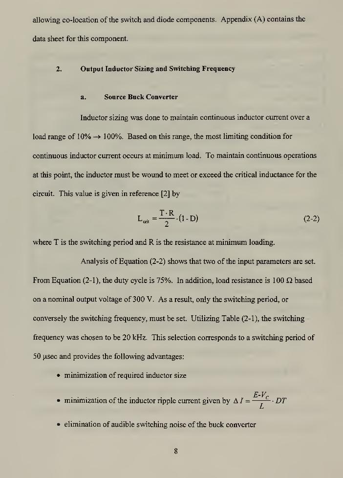
System transient analysis focused on investigating a step load change from 300 W
to 3 kW on the output of the Load Buck Converter. Figure (5-2) documents the results.
As can be seen, the output voltage and current of the Source Buck Converter (Vout and
ioutl) have a somewhat more pronounced oscillation at the transient edges before settling
to steady-state values. This result is due to a "ringing" effect set up between the output of
the Source Buck Converter and the input LC filter of the Load Buck Converter. In fact,
this effect is clearly discernible in ioutl in the steady state. The transient performance of
the Load Buck Converter is the same as that predicted by Figure (4-7) in Chapter IV.
With system stability demonstrated, a hardware validation study was conducted.
Figure (5-3) shows the actual system response for a 300 W to 2.5 kW load change. The
reason for the difference between the simulated 3 kW maximum load value and the actual
2.5 kW load value was based upon the sizing of test load banks available in the
laboratory. Comparison of the simulation and hardware trials demonstrates reasonably
good correlation between predicted and actual system response. Note that the voltages in
Figure (5-3) are ac coupled. The major difference between the plots comes from the
switching harmonics and noise of the actual system operation. The principle source of
the noise comes from the operation of the IGBT switches.
C. MODE 2 OPERATION
Mode 2 is defined as a Source Buck Converter operating in series with an
inverter. Figure (5-4) illustrates the overall system model. A hard-switched inverter
was used to model the ARCP unit so that simulation times could be kept to a reasonable
37
Vout Response
20
« 15Q.
i 10
2 5
50 60 70 80 90 100 110 120
ioutl Response
j. i ij i i i 1 a. 1 j.
i i [ i i i i | i i i i
i i i i i ili i i i
_,
—
j—
,
. . r— —| r , T
30 40 50 60 70 80 90 100 110 120
to
CO
215
210
2 205
> 200
195
15
2. 10E
1 5o
30
Vout3 Response
i I 1 I I I V J 1 I 1
i i y\ ' ' ' -\ L ' l
; i I / . i . . i \ i / i r
i '__ 1j ii i i__\_ ll " i
: f ; : : : V :
1 I i- J I I I » L I J.
30 40 50 60 70 80 90
iout3 Response
40 50 60 70 80
time (msec)
100 110 120
I
1
1
1
. _ 1
J/~» ' ' '—
1
1 1 1 1
1 1
) J.
1
1
1
1 _ .
1
1
1
1
. _ 1 1 1 1 1 . 1 J
1
1
1
1 _ .
1
1
1
1
1
1
1
1
90 100 110 120
Figure 5-2, Mode 1 Simulation Results: 300 W —> 3 kW Load Buck Transient
38

Vout Response (ac coupled)
20 40 60
ioutl Response
100
CO
Z3o>
ICO
o
15
10
5
Vout3 Response (ac coupled)
40 60
iout3 Response
T T
i j.
i
100
l*WtWiil li i intfii
Vy«'^^^
i i
j. i_
20 40 60
time (msec)
80 100
Figure 5-3, Mode 1 Hardware Results: 300 W —» 2.5 kW Load Buck Transient
39

length. Since the gross system dynamics between an ARCP and a conventional inverter
are nearly the same this assumption was reasonable to make. The inverter was controlled
by a current feedback controller implemented in the stationary reference frame. A
complete discussion on the derivation of this model is given in reference [8]. As with
Mode 1 operation, the input filter capacitor and its associated ESR had to be modeled as
an equivalent parallel combination in the ACSL code.
iLfiltl 8&E £2
IGBT Module
(2 V drop)
0-
Diode
(2 V drop)
Rlesrl
02 ohms
Lbuckl760 uH
Cbuck .400uF '
Rcesrl
0.01 ohms
ioutl
Rout
(9.68 to
96.8 ohms)j
Onv .
Vout lOuF'
IN S2X S3X
X S5X S6X
Figure 5-4, PEBB Testbed Mode 2 Operation
System transient analysis focused on investigating a step change in load from
2.5 kW to 6 kW at the inverter output. This was performed by changing the amplitude
values of the reference phase currents from 10 A to 24 A. Figure (5-5) documents the
results. As can be seen, significant switching harmonics have been introduced into the
output voltage and current responses of the Source Buck Converter. In addition, this
effect is aggravated at higher levels of inverter loading. The output of the inverter is as
expected for a current controlled unit.
40

Vout Response
COQ.
ECO
30
20
10
3g
-10
ioutl Response
' Mall i^rVIBrYl^tYLBMMfTnM—
'
20 40 60 80 100 120
200
(ACO
> -100
20
« 10a.ECD
CO-10
-20
20 40
Vas Response
60 80
iLa Response
60 80
time (msec)
100 120
i 7 \" F\~ 7 \ '
i / \ i
I \ ' / \ '
_ / l r 1 \f
L. _ J ^ _ __
\ I \' / 1 ' J \ ' / \ /I \ I \l I \ I
II ' / \ /
r \ r b- f A - t - t r— if "V 7
-
1 \ / I / \ ' / \ J \ /1
\J J— J. y t -/ \~r"•
1»
'\ ! V ' / \/ '
1 1 \ / V 1 /"
1
100 120
Figure 5-5, Mode 2 Simulation Results: 2.5 kW -» 5.3 kW Inverter Transient
41

One point to note is that the inverter current response does not achieve the desired
steady-state values. This result stems from the use of stationary reference frame control.
Although it is easy to implement, reference [8] shows that steady-state errors of 11% can
be expected. A hardware validation study was not conducted for this case because the
ARCP closed-loop control has not been fully developed at this time. It is anticipated that
future research efforts will provide the hardware study results to validate these
waveforms.
D. MODE 3 OPERATION
Mode 3 is defined as a Source Buck Converter supplying both a Load Buck
Converter and an inverter. Figure (5-6) illustrates the overall system model. The same
inverter model described in Mode 2 operation was used for this case. As with Mode 1
operation, the input filter capacitor and its associated ESR had to be modeled as an
equivalent parallel combination in the ACSL code.
IGBTNfodile
(2 V drop) RIesri -
02 ohms
Rout3(144 to > Vout3144 ohms) ^
Figure 5-6, PEBB Testbed Mode 3 Operation
42

Transient analysis focused on investigating system response to the load changes
discussed in Mode 1 and Mode 2 operation. The step change for the Load Buck
Converter occurred at 45 msec while the step change in inverter loading was specified at
125 msec. Figure (5-7) documents the results. The plots show a system response that is
the composite of the results achieved in the previous two modes of operation. As with
Mode 2 operation, a hardware validation study was not conducted since the ARCP
closed-loop control algorithm is still under development.
E. MODE 4 OPERATION
Mode 4 is defined as parallel Source Buck Converter operations. Figure (5-8)
illustrates the overall system model. As described in Mode 1 operation, the input filter
capacitors and their associated ESRs had to be modeled as equivalent parallel
combinations in the ACSL code.
Transient analysis for this case focused on investigating a load change from
2.25 kW to 18 kW and observing system response. Figure (5-9) documents the results.
From the plots, it can be seen that the parallel units share the total load, iout, equally. In
addition, the output voltage response covers the full range of house curve operation as
expected.
An interesting occurrence to note in the individual buck converter current
responses, ioutl and iout2, is the "mirror" effect seen at the transient edges. This effect is
best observed in the system transient at the 85 msec mark. At this point, ioutl settles to
43

Vout Response
£ 304
$ 302r 300o 298> 296
CO
I 20
& 10
^ 2200)
1210 L-^-i IJX-i 1 1 4CO
1 200
20
80 100 120 140
ioutl Response
I IV 4- * -'—"+ + 4 •* -
200
L -- --- _ MM MMM j
20 40 60 80 100 120 140 160 180 200
Vout3 Response
r-V r T T
40 60
T T
80 100 120 140 160 180 200
^ 20COQ.
3, 10
$2"3
2
1.
.
200
~ 20
iout3 Response
-I. J. ± i. J. 4 -1
40 60 80 100 120 140 160 180 200
Vas Response
60 80 100 120 140
iLa Response
160 200
100 120
time (msec)
Figure 5-7, Mode 3 Simulation Results: Load Buck and Inverter Transients
44

iLfiltl Rlesr inl iswl0.2ofims
IGBT Module(2 V drop)
Vin Diode
(2 V drop)
Rlesrl
0.2 ohms_litfti__vVVV—Lbuckl760 uH
Cbuck400uF '
Rcesrl
0.01 ohms
ioutl
flLfilt2 Rlesr in2 isw20.2ofims
IGBT Module
(2 V drop)
Diode •
(2 V drop)
Rlesr2 Joul20.2 ohms __*.
Lbuck2875 uH
Cbuck400uF '
Rcesr2
0.01 ohms
lout
Vout
Rout
(9.68 to
96.8 ohms)
Figure 5-8, PEBB Testbed Mode 4 Operation
its final steady-state value following a slight undershoot. The response for iout2, on the
other hand, settles to its final steady-state value after experiencing an overdamped effect.
When observed on an expanded scale, the currents are mirror responses of each other.
This result occurs due to the difference in the output inductor sizing of the Source Buck
Converter units. In essence, a small AC current is established and reflects between the
paralleled capacitors based upon the difference in the inductor current waveforms.
With system stability demonstrated and the transient excursion of the variables
well within device limitations, a hardware validation study was conducted for Mode 4
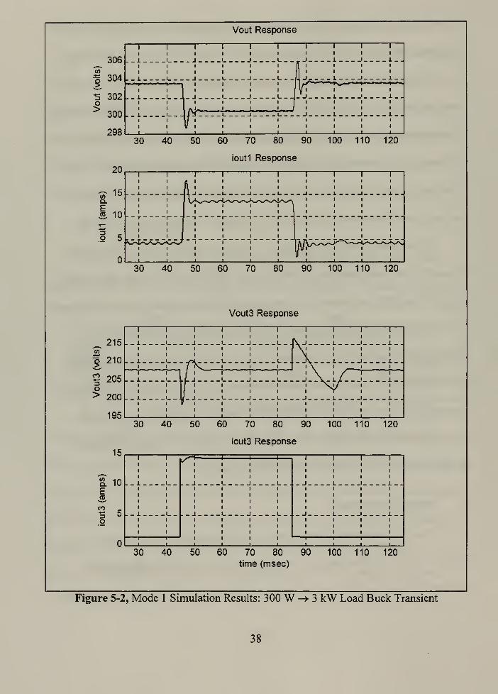
operation. Figure (5-10) shows the actual system response for a 2.25 kW to 7.5 kW load
change. Although the overall transient was smaller in magnitude, a general comparison
of the simulation and hardware trials demonstrates reasonably good correlation between
predicted and actual system response. As with the Mode 1 hardware validation, the major
45

Vout Response
20
60
| 40
CD
20
60 80
iout Response
40 60 80 100
120
I. ... 4. 4 1
.
r T ,
120
30
"at
O.E 20as,
a 10
20
30
"toa.
E 20
a 10
20
ioutl Response
I I I I
L_ t' _ 2 _'
40 60 80
iout2 Response
40 60 80
time (msec)
100
100
120
•
J
# - n ni»! f rn nil Bin —
I r r 1
. | . «. 4 1
- - ! I ! k. !
120
Figure 5-9, Mode 4 Simulation Results: 2.25 kW -> 18 kW Load Transient
46

difference between the simulated and actual results is due to the presence of switching
harmonics and EMI noise in actual system operation.
The current "mirror" effect discussed previously is demonstrated on an expanded
scale in Figure (5-11) for actual circuit operation. It can be seen that the effect occurs
during steady state as well as transient operations. The steady-state effect was not as
noticeable in the simulation because switching noise was not modeled. Follow-on
research may consider incorporating a Gaussian white noise source into the sensed
variables in the simulation.
F. MODE 5 OPERATION
Mode 5 is defined as two parallel Source Buck Converters operating to supply one
Load Buck Converter. Figure (5-12) illustrates the overall system model. As described
in Mode 1 operation, the input filter capacitors and their associated ESRs had to be
modeled as equivalent parallel combinations in the ACSL code.
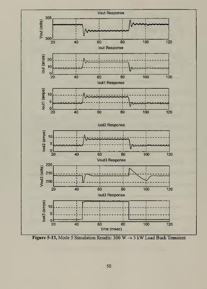
System transient analysis focused on investigating a step change in resistive load
from 300 W to 3 kW on the output of the Load Buck Converter. Figure (5-13)
documents the simulation results. As can be seen, the output voltage and current of the
parallel Source Buck Converters have a somewhat more pronounced oscillation at the
transient edges before settling to their steady-state values. This result is due to a
"ringing" effect set up between the output of the Source Buck Converter and the input LC
filter of the Load Buck Converter. During load transients, this effect dominates over the
current "mirror" effect documented in Mode 4 operation. This result is shown in
47
Vout Response (ac coupled)
=3o>
^ 2010Q.
i 10
3.2
^ 20COQ.
«. 1
3O
20 40 60
ioutl Response
100
m. "....jSnittaAli.. LmMP.
20 40 60
iout2 Response
80 100
2
+m L_--Jtf*#WV*^it?
w^iWW^20 40 60
time (msec)
80 100
Figure 5-10, Mode 4 Hardware Results: 2.25 kW -> 7.5 kW Load Transient
ioutl Response
20
«r isQ.E -„«, 10
.2 5
20
*+***\fl^^
T
^^^^li^/^S^
4 6
iout2 Response
10
15
3, 10
"3
o
I I I I
1 1 I 1
1 1 1 1
t^w**^^1
1
1
1 1 1 irf***"^1 1 1 1
1 1 1 1
1 1 1 1
1 .1 1 . 1 ...
4 6
time (msec)
10
Figure 5-11, Mode 4 Hardware Results: Current Mirror Effect
48

IGBT Module
iLfihl RJesrinl j^,OV*op) w=rl ioutl
IGBT Module
iLfik2 Rlesrin2 isw2(2VdroP) Rlcsr2
02 ohms
iLfilO Rlesr in3— 0.2 ohms
LflB425 uH
Cbi3460 uF
ICBT Module
(2 V drop)
~VDiode
(2 V drop)
Rccsr in3:
001 ohms
Rlesr3
02 ohms
Lbuck31300 uH
Cbuclc3 3400 uF
Rcesr3 <
001 ohms 1
RoutS
(14 4 to £ Vom3144 ohms)'
Figure 5-12, PEBB Testbed Mode 5 Operation
Figure (5-13) by observing that the transient portions of the output currents, ioutl and
iout2, are "in phase" with one another during load changes.
With system stability demonstrated, a hardware validation study was conducted
for Mode 5 operation. Figure (5-14) shows the actual system response. From the plots, it
can be seen that the actual Load Buck Converter output correlated with the simulation
results. Actual current values out of the parallel Source Buck Converters were about
2.5 A higher than shown in the simulation results because a 25 Q static load was used
during hardware validation. In the ACSL simulation, this value was 40 Q. The voltage
output response of the parallel Source Buck Converter is harder to compare due to the
switching noise present on the waveform. Note that all voltage responses are ac coupled.
The "ringing" effect versus the current "mirror" effect is shown in Figure (5-15).
This plot shows how the mirror effect dominates during steady-state operation but shifts
"in phase" during load changes. Overall, comparison of the simulation and hardware
49
305
1
o> 300
(Aa.
E05
CO
20
20
r 10
-20
(AQ.
g 10 r--Av-"
5
20
—*i.
40
40
40
Vout Response
60 80
iout Response
60 80
ioutl Response
«L».«.i ^^•^•^•^
100
100
60 80 100
120
• J\7C^JlC-Lr^ZJC-Z^_ZJU3-Z^L 1
120
- 1 --|jva«>
|*wMw
120
^ 220CO
9. 210CO
g ^"0>
^
(OQ.
E 10(0
CO 53o
20
20
iout2 Response
60 80
Vout3 Response
i j.
40 60 80
iout3 Response
40 60 80
time (msec)
100
:iXZ:IZT."34_> i
100
100
120
120
%> > 'Ii i i i
I1 7 1
120
Figure 5-13, Mode 5 Simulation Results: 300 W -> 3 kW Load Buck Transient
50

5
Vout Response (ac coupled)
1°
> -5
k^J^^ i^M(
^ 20
3 20 40 60
iouti Response
80 100
COQ.
s 10
•°
*ift*
1
1
i i
i i
i
i
>
***
)0
30
30
30
(
— 20
J 20 40 60
iout2 Response
80 k
co
JL 10CN
P^yv
1~
i
1 1
i
vws
(
10
) 20 40 60
Vout3 Response (ac coupled)
80 K
1 °
> -5
-10
#^f«
1
i
i
i
I ii
J i
i
i l
i i
1
i
i _
rV ' 'L \i j^ i
il|r
i r
i
^L! iH 1
i
\ J)l
1 ' ' '
i i i
i i i
f i
| i
() 20 40 60
iout3 Response
80 1(
15
CO
en 5
3 o
-5
1
i 11
i
i
i i ri i
A _ L s\ _ j i.
i i
i i
i i
jpffwv
(3 20 40 60
time (msec)
80 1(
Figure 5-14, Mode 5 Hardware Results: 300 W -> 2.5 kW Load Buck Transient
51

trials demonstrates reasonable correlation between predicted and actual results. As with
the previous hardware studies, switching noise constitutes the major difference between
simulated and actual operations.
ioutl Response
en
03
15
10
5 5
^/V^1*f H|. ^A^Vvvv^
40 45 50
iout2 Response
55 60
15
f 5 \/\/fi>fh»A
40 45 50
time (msec)
55 60
Figure 5-15, Mode 5 Hardware Results: Current Mirror Effect
G. MODE 6 OPERATION
Mode 6 is defined as two parallel Source Buck Converters supplying an inverter.
Figure (5-16) illustrates the overall system model. The same inverter model described in
Mode 2 operation was used for this case. As described in Mode 1 operation, the input
filter capacitors and their associated ESRs had to be modeled as equivalent parallel
combinations in the ACSL code.
52

Rlesrl ioutI0.2 ohms _
Lbuckl760 uH
Cbuck ,400uF "
Rcesrl
001 ohms
IGBT Module
ifilG Rlesr in2 isw2(2Vdrop)
Rlesr2
0.2 ohms
Lbuck2875 uH
Cbuck _400uF '
Rcesr2
001 ohms
iout2
Vout ,
Rout
(9.68 to
96.8 ohms)
Cinv .
IOuF'
SIX S2X S3\
Figure 5-16, PEBB Testbed Mode 6 Operation
System transient analysis focused on investigating a step change in inverter load
from 2.5 kW (10 A peak current per phase) to 6 kW (24 A peak current per phase) and
observing system response. Figure (5-17) documents the results. As can be seen,
significant switching harmonics have been introduced into the output voltage and current
responses of the parallel Source Buck Converters. In addition, the level of the harmonics
is increased with increased in inverter load. The output of the inverter is as expected for a
current controlled unit. As described earlier, the inverter current response does not
achieve the desired steady state-values due to the use of stationary reference frame
control. A hardware validation study was not conducted for this case because the ARCP
closed-loop control has not been fully developed.
53

305w
o> 300
20
a.
E 20CON—
*
103O
U
"wQ.
F 10CD
^_ 53g
Vout Response
40 60 80
iout Response
100 120
60 80
ioutl Response
120
(/>
CL
E 10mCN fa
3g
20
9
03
> -200 t
~ 20COQ.
I o
CO
:=! -20
20
iout2 Response
TTfTTT™" rffTTT'
40 60 80
Vas Response
100 120
60 80
il_a Response
i / \ i / \ ' / \ '
i / \i / \ ' / \ ' /™\ yi £ v / A _ a _ j V — j/— \ y.
40 60 80
time (msec)
100 120
Figure 5-17, Mode 6 Simulation Results: 2.5 kW —» 5.3 kW Inverter Transient
54

H. MODE 7 OPERATION
Mode 7 is defined as two parallel Source Buck Converters supplying both a Load
Buck Converter and an inverter. Figure (5-18) illustrates the overall system model. The
same inverter model described in Mode 2 operation was used for this case. As
described in Mode 1 operation, the input filter capacitors and their associated ESRs had
to be modeled as equivalent parallel combinations in the ACSL code.
KBT Module
iLfiltl Rlesr>! aw)P v *°l>)
CbucU X Rout!400uF ~ (144to ^ Voul3
144 ohms) rRob30.01 ohms 1
Figure 5-18, PEBB Testbed Mode 7 Operation
System transient analysis focused on investigating the transients discussed in
Mode 5 and Mode 6 operation and observing system response. Figures (5-19) and (5-20)
document the results. The step change for the Load Buck Converter occurred at 45 msec
while the step change in inverter loading was specified at 125 msec. These plots show a
system response that is the composite of Mode 5 and Mode 6 results.
55

308
Vout Response
^ 306CO
i- 304
O> 302
300
1
1
1
1
i
i
i i i i
i i i iiiii i
i
i
I
i
i
)0
1
1
1
1 1
1
i
i
i
i | i i
i Jl i ifi
II.. .
_i „^.,^^,l.,»/
1 In '
i
i
i ! 1 1 1
1
i
i
i
T* ' ifi y
~ -
i
i
ili i i i
i i i i i
i i i i
i
20
30
40 60 80 100 120 140
iout Response
160 180 2(
» 20
!
1 1 Iiii|| r 1
I I
Ij
W... iiii2 40 60 80 100 120 140
ioutl Response
160 180 200
15"ST
|10CO
i:-5
1
_ _ L _
1
i
L
iiiiiiiii i i i
I
i
j
I
i
_ _i
ij~ iiiii i
i Mi i i i i i i
~*
i i i i i i i i
i i i i i i i
2 40 60 80 100 120 140
iout2 Response
160 180 200
15"ST
gioCO
i:-5
1
i
_ _ L _
l
t
L _ _
i i i Iiiii__i i i i__
I
i
i
I
i
. j
il
^^^^^^^^^
i i iiH|.
. ......i-.li i i
u1 1 1 1 1 1 1 1
1 1 1 1 1 1 1 1
1 1 1 1 1 1 1 1
2 40 60 80 100 120 140
time (msec)
160 180 2()0
Figure 5-19, Mode 7 Simulation Results: Load Buck and Inverter Transients
56

Vout3 Response
20
S 15Q.
s 10CO
1 5
20
?15
I
L .
1
i
L
I
i
_ i
.
1
V. i
I
1
I
i
_ ±
I
i
i
I
i
_ j
(volts) O
l
L _ .. 1_
\ i
\ i
1
1
1
i
i
i i j
,,.,„„!„ ^
\ iL _
1 i
2 205 . L . ! i _
1
1i
i i i3 *""O> 200 L . ! j.
VI1
1
i
i A
195
I I I I I I I r
I I I I I I I I
i i i i i i
2 40 60 80 100 120 140 160 180 2C
v—
40 60
iout3 Response
80
L _ ^ L L J. J. J. J. 1
100 120 140 160 180 200
Vas Response
200=^
80 100 120 140
i La Response
100 120 140
time (msec)
180 200
200
Figure 5-20, Mode 7 Simulation Results: Load Buck and Inverter Transients Continued
57

I. SUMMARY
This chapter has included a discussion of the ACSL simulations performed for
seven basic PEBB Network configurations. The results of these simulations did not yield
any gross system instabilities. At most, only "interesting" system interactions were
identified. In addition, hardware validation studies were conducted for Modes 1, 4 and 5.
The results of these tests verified that the ACSL simulations correlated well with
hardware implementation. The hardware validation results also showed that switching
noise was a major issue in actual circuit operation. Chapter VII addresses methods for
eliminating or minimizing the switching noise and suggests follow-on ACSL simulations
and hardware validation studies.
58

VI. SCHEMATICS
A. CIRCUIT BOARD BACKGROUND
1. Easytrax Overview
The development of printed circuit boards (PCBs) was done using Protel
Easytrax, version 2.06. This software allowed PCB definition, layout, and component
interconnection on two layers. All PCB layouts were done so that there were no isolated
ground sections. Once a PCB was developed, a netlist was compiled. The basic function
of the netlist is to associate integrated circuits with resistors, capacitors, and diodes so
that connections can be verified. With the PCB layout completed, a Gerber file was made
to direct the required circuit milling. The milling work was done at the Naval
Postgraduate School by DPI Daly. Finally, hardcopies of circuit traces and component
layouts were made for future reference.
2. Circuit Labeling
For the purpose of more easily locating components and understanding their
function in the circuit, the following format was chosen:
The first digit represents the type of component.
• R: resistor
• C: capacitor
• D: diode
The second digit represents the IC with which the component is best associated.
59

• 0: U10
• 1: Ul
• 2: U2, etc.
The third and fourth digits are used for IC pin location.
• 03: pin 3
• 18: pin 18, etc.
When a prefix is used, it indicates an interface between circuits in the overall system.
The prefix may have an actual number associated with it or just the '#' sign.
• SI : Sensor board interface for buck converter 1
• D#: Driver board interface for buck converter being referenced
• J25: 25 pin D-sub connector interfacing controller with other boards
If a suffix is used, then there are generally more than one of the same components
connected to the same pin.
• A,B,C: Multiple components of same type are connected to same pin
where A = 1 component, B = 2 components, etc.
• G: Ground
• H: Vcc, Vdd: positive source voltage
• L: Vss: negative source voltage
• Q: Transistor
Specific examples of circuit labeling include:
• C#-J25-9: Control board interface at J25 pin 9 for buck converter being
referenced.
60

• Rl 13C: Resistor connected to Ul pin 13 and there are at least two more
resistors connected to that same node.
• C006: Capacitor connected to U10 pin 6.
• RJ4036Q: Resistor connected to J40 pin 36 and a transistor.
B. CIRCUIT DIAGRAMS AND DESCRD7TIONS
This section documents the hardware implementation of the Source and Load
Buck Converters as well as their associated sensor, controller, and driver boards. Each
subsection is layed out so that it contains a detailed line diagram and description of the
circuit. If further information is needed, Appendix (D) contains all the Easytrax PCB
schematics and netlists.
1. Source and Load Buck Converter Topologies
Figures (6-1) and (6-2) document the layout of the Source and Load Buck
Converters. As seen from the diagrams, the topologies are identical. Input/output
characteristics, inductor sizing, and the voltage sensing circuits represent the only
differences. The reason for the different sensing circuits goes back to the choice of
analog control boards for the Source Buck Converters and digital control boards for the
Load Buck Converters. As the diagrams indicate, the analog controller requires a voltage
reduction of (1/50) whereas the digital controller requires a voltage reduction of (1/100).
The general flow of overall system operation is as follows:
• Sensed voltage from the voltage divider network is sent to the sensor board
via twisted pair.
61

• Sensed currents are sent to the sensor board via the Hall Effect sensors.
• The sensor board, acting as an isolator, provides the appropriately scaled
voltages and currents to the analog/digital control board.
• The control board processes the voltages and currents according to the
developed control algorithm.
• The generated driver signal from the control board is sent to the IGBT driver
board via twisted pair (analog control) or optical signal (digital control).
(S1-R703)
(S2-R803)
425 uH
nmnn
IGBT Module
(D-R106. R107,DGA^)
Driver
Common
Sl-TWin+S2-TWin+
10K%(ViiVS0)'
Sl-TWin-S2-TWin-
Figure 6-1, Source Buck Converter Topology
(S1-R703)
(S2-R803)(S1-R503)
(S2-R603)
IGBT Moduleio/1000
425 uH
mnrm
Figure 6-2, Load Buck Converter Topology
62

• The driver signal controls the IGBT switching frequency and duty cycle.
With this overview in hand, a more detailed description is presented next.
2. Sensor Board
Pictured in Figure (6-3), the sensor board provides isolation between the buck
converter and the analog/digital control board. Sensed voltages from the voltage
divider network on the buck converter are sent via twisted pair to the input of wideband
AD215 isolation units. Configured as a unity gain buffers, the AD215s output the sensed
voltages and send them to the control board via twisted pair. Current sensing is done by
CL50 Hall Effect sensors mounted directly on the sensor board. Instantaneous currents
proportional to (isense</1000) are output by the Hall Effects. These currents are converted
to a proportional voltage by 100 Q. precision resistors to yield (isense</10)- These voltages
are the sent to the control board via twisted pair.
3. Analog Control Board
The implementation of the analog control board can be broken down into five
subsections:
• J25 - 25 Pin Connector and Buffer Stage
• Main Control Stage
• Pulse Width Modulation Stage
• Protection and Startup Circuitry Stage
• Power Supply Stage
63

A diagram and discussion of each of the subsections is provided below. Appendix (D)
contains detailed PCB information on the analog control board.
2K(W50)' Rioi
Sl-TWout+ e f WW-
Buckl
Sl-TWout- •-
ID1011N5240
E
Sl-TWin+
Sl-TWin-
NC-
NC-
2KQMSOy R301
,
36
38
AD215IN+ Ul TRIM NC
INCOM OUTLO3?
IN- OUTHI
FB +15 Vin
-Viso PWRRTN
+Viso -15 Vin
+15VO—
(V<V50)'
C1-J25-9
C1-J2S-22
-15 VO—
-O+Vs
CL50U5~
-O -VsOUTO-
(i<yio)'
> C1-I25-7
*-VWW-> ci-
0.1 K V-15 V R503
D3011N5240
ENC-
NC-
AD215IN+ ^ TRIM
INCOM OUTLOIN- OUTHFB +15 Vin
-Viso PWRRTN+Viso -15 Vm
NC
+15 V
(Vin/50)'
C1-I25-8
C1-J25-21
+15 V
-15 V
CL50 .
UJ-rflUlO)'
O.IKOUT • ^ n t?s i<
(W50)'
S2-TWout+
S2-TWout-
Buck2
ENC-
NC-
INCOM OUTLO
TN- OUTMFB +15 Vin
-Viso PWRRTN
+Viso -15 Vin
NC
+15 V©—
+15 V
(Vo/soy
C2-J25-9
C2-J25-22
-15 Vo—
-O+Vs
CL50,U6H
—O -VsOUT
Oo/ioy
> C2-J25-7
O.IK
-15V
MMAr£->R603 V
C2-J25-20
S2-TWin+
S2-TWin-
(W50)'36
38
AD215IN+ W TJUmY— NC
INCOM OUTLO
-
IN- OUTMFB +15 Vin
-Viso PWRRTN+Viso -15 Vin
(Vin/50)'
C2-J25-8
C2-J25-21
+15 VO—
-15 V-15 Vo—
-O+Vs
CL50U8-
OU?©-
(iU10)'
> C2-J25-6
OIK*-VWv±->
RS03 V0-J25-19
Bypass Capacitors
+15 VUl-42
I TI7815
VR1_ 1N4O05 _k DVRllA''
flN4005 _DVR11B
i
^1N4005 _DVR22B
J 2200u
2CVR11
J 2200u"=
2CVR22
2
28 Vc h117 Vac flL
2- 1N4005 -k DVR22A'i
i
MC79I5VR2
U1,U2,U3,U4 = AD215U5, U6, U7, U8 = CL50 Hall Effect Sensor A
0.1 u
-15 VU1-+4
C142 C144
-15V
+15VU5
VC501
-15VU5
+15 VU2-42
1
2
VC242
+15 VU6
-15VU2-44
+15 VU3-42
-15 VU3-44
+15 VU4-42
C244 042 CJ44 C442
-15 VU6
C502 C601 C602
+15 VU7
1
2
VC701
-15VU7
C702
+15 VU8
-15 VU444
C444
-15 VUS
C801 C802
Figure 6-3, Sensor Board
64

a. Buffer Stage
From the twisted pair output of the sensor board, the sensed and scaled
voltages and currents go to the 25 pin D-sub connector of the control board as shown in
Figure (6-4). From J25, the inputs are buffered utilizing a LM324 quad op amp (labeled
U2). Each buffer stage input contains an RC lowpass filter designed to remove high-
frequency components from the measured voltages and currents. The cutoff frequency
for each filter is at 8 kHz. The LM324 outputs are fed to the Main Control Stage.
b. Main Control Stage
The Main Control Stage is where Equation (2-18) is formulated. The
output of this stage is the analog duty cycle scaled by a factor often. In addition to the
Buffer Stage outputs, the signal representing the desired output voltage is fed into the
Main Control from the Protection and Startup Circuitry Stage. As shown in Figure (6-5),
an AD534 configured as a divider provides the base duty cycle, D^, by dividing the
reference voltage by the input voltage. Note that this arrangement implements the
feedforward term given in Equations (3-18) and (3-19) of Chapter III.
The small-signal control algorithm is performed using a LF347 quad op
amp. The first three op amps in the package form the proportional voltage (Ul ,), integral
voltage (Ul 2)and current response (Ul
3) terms. Note that a limited integrator has been
used to generate the integral voltage term. This implementation prevents integrator
windup. Without the limiting zener diodes in place, CI 07 is free to charge up during
extended transients to values well outside the range in which its voltage affects duty
65

cycle. As a result, the voltage on CI 07 locks out the remaining terms in the duty cycle
control algorithm. This lockout persists until CI 07 come backs within its operating
range. The final op amp (Ul 4) is used to scale and sum the outputs of the first three op
amps. Scaling is performed such that the analog gain values developed in Chapter IV
were obtained, scaled by a factor often. Output feeds the Pulse Width Modulation Stage.
J25-I3
J2S-25
+ Drive Pulse
(U3-»)
o—
I
C#-;25-9
C8-J25-22
(Vo'soy 2KO WW
R203
(Vin/50)' 2K
C#-J2S-8 O WWR205
OJ25-21
n,
(\u\oy 2 K
CM-J25-6 O WW-R210
OJ25-I9 nfio'10)' 2 K
OJ2S-7 O WW-R212
OJ25-20 1
-> EW-TW+
-> tW-TW-
-13.5 V
: 01 u
C205
: ooi u
C210
:ooi u
ai2
,U2 ^>—fc
Vin/50
(U4-D
iI710
(Rl 10. U3-12)
ia'10
Over Temperature / Vref Reset
+5VJ2S-4
J25-3 > <- Vrd—
>
J25-I6
J25-1
V^
J2S-2 ssJ25-14 ssJ25-15 "s^>
J25-24
/7w
125-5, 10, 11, 12
o—
(RI09, R102A.R411.R316B)
US-1.R501.CS01
Chassis Ground
Unused
Reset Switches
1Mi—VWV—
i
4KM v
Bypass Capacitors
+13 5 V -13.5 VU2-4 U2-11
Ci cj>
01 u 9C204
5 ? ^ 0.1 u
an
\7 \7
u > = LM324
Figure 6-4, Analog Control Board: J25 - 25 Pin Connector and Buffer Stage
66

-Vref/50
10
3i5|9|.3|
(U6-7, R607, R102B)
22
XI
X2
Zl
Yl
Y2
NC -Vs
AD534 +VsU4
SF
our
1
Vin/502
(U2-6.7) $ 11
^~6
^T" 7
r
Bypass Capacitors
-13.5 V
+13.5 V
NC
io/10 (U2-13, 14.R316B)
UV10o(U2-8, 9, U3-12)
-Vref750
o(U6-7.R607,
U4-10)
Vo/50
o(U2-1, 2)
R102B
-13.5 V 13.5 V 13.5 V -13 5 VU4-8 U4-14 Ul-4 Ul-U
O1
o1
o1 9.
?«? 3«C ?K2 2 2 2
V V V VC408 C414 C104 cm
R102C
20 K
WWiR113A
13 K
-^AAAHR113B
15K 20 K
AAAArf—AAAAa—i
R114
- 13.5 V
Voltage
Reference with
House Curve
Grounds
U4-2, 6, R41 1G-1, C408-2, C414-2, C104-2, CI 1 1-1
Ul-3,5,R110G-2,R112G-2
U1=LF347
U4 = AD534
Figure 6-5, Analog Control Board: Main Control Stage
c. Pulse Width Modulation Stage
Pictured below in Figure (6-6), the Pulse Width Modulation (PWM) Stage
is comprised of the UC3637 chip. It receives the analog duty cycle from the Main
Control Stage and produces a square wave driver signal with a frequency of 23 kHz based
upon R3 1 8 and C302. This frequency can be calculated utilizing formulas given in the
UC3637 data sheet in Appendix (A). Actual frequency runs about 20.5 kHz due to
67

interactions with the phase-locked loop circuit described below. The duty cycle of the
pulses is equal to the Main Control Stage analog duty cycle signal divided by ten. From
the Pulse Width Modulation Stage, the driver signal is fed to a driver board mounted on
the IGBT.
10d(t)
O(U1-RR114)
iiyiO(U2-8,9,R110)
1.3 KR311
^AAAr0.01 u
Oil
Shutdown
(R807R R807, C807)£
Shutdown
Circuit {^
13 K
R313
10 K.
!R313G
0.22 u
C313
+13 5 V
U3 = UQ637
Grounds
U3-3, 15, Oll-l, R313G-2, C313-2, D301-A
C30I-1, C302-1, O06-1, O05-1
- Ain - Bin
+Ain UC3637 +Bin
+OL U3 Bout
-C/L +Vs
S/D -Vs
+E/A Aout
- E/A - Vth
E/AOutput Qbet +Vth
7~*' 2*1^— Ml" VNC
,. PLL-R102* (MASTER)-^ PL^R202• (SLAVE)
Q=1000pFC302
+13.5 V
-13.5 V^ Drive Pulse
J25-13
T^ 0.36 K (MASTER) J—
O
0.47 K (SLAVE) ^ J2<L-
51K(MASTER)62K (SLAVE)R31S
10V .
D301 '
1N5240
AAAAr-0+i3svJ25-25
0.47 u
C301
R301
-13.5 V
SLAVEOMJ3-18(PLL-R311X)
Bypass Capacitors
13 5 V -13.5 V
O.u I' l 0.1 u
O05
Figure 6-6, Analog Control Board: Pulse Width Modulation Stage
d. Phase Locked Loop
Analysis of Figure (6-6) shows MASTER and SLAVE connection points
for implementation of the Phase-Locked Loop Board shown in Figure (6-7). This board
synchronizes the switching frequencies of both Source Buck Converter controllers so that
they can operate in parallel. Without proper synchronization, load sharing between
paralleled units cannot be achieved due to inductor current oscillations. As shown in
68
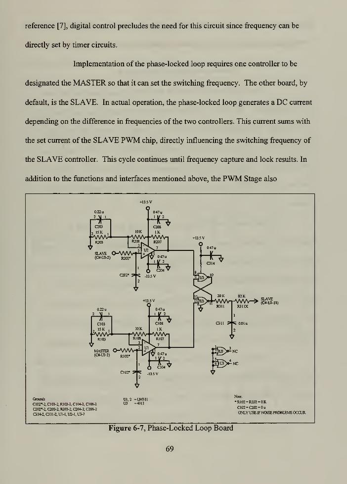
reference [7], digital control precludes the need for this circuit since frequency can be
directly set by timer circuits.
Implementation of the phase-locked loop requires one controller to be
designated the MASTER so that it can set the switching frequency. The other board, by
default, is the SLAVE. In actual operation, the phase-locked loop generates a DC current
depending on the difference in frequencies of the two controllers. This current sums with
the set current of the SLAVE PWM chip, directly influencing the switching frequency of
the SLAVE controller. This cycle continues until frequency capture and lock results. In
addition to the functions and interfaces mentioned above, the PWM Stage also
0.22 u
2 \| I
+13.5 V
o
C203
2 I5K1
fA/vW*R203
SLAVE(OMJ3-2)
10K
R208
2|U2
0.47 u
•HftC208
IK
R207
R202'
C202*
D047 u
Q C204 v
C102*-13.5 V
Grounds
C102*-2, C103-2, R103-2, C104-2, CI08-2
C202*-2, C203-2, R203-2, C204-2, C208-2
C314-2, C311-2, Ul-1. U2-1, U3-7
U1.2 = LM311U3 =4011
+13 5 V
Q0.47 u
a 14
on
NC
NC
Note:
•R102 = R202 = OKC102 = G02 = 0u
ONLY USE IF NOISE PROBLEMS OCCUR
Figure 6-7, Phase-Locked Loop Board
69

provides pulse-by-pulse and overcurrent protection circuitry. These circuits are
documented in the following Protection and Startup Circuitry Stage discussion.
e. Protection and Startup Circuitry Stage
The analog controller provides the Source Buck Converters with two
forms of protection. The first is the pulse-by-pulse current limiting feature of the
UC3637 chip. This circuit protects the IGBT from exceeding its 90A current rating.
Referring to Figure (6-6), pins 12 and 13 make up this circuit. If a fault occurs in the
buck converter, iL/10 will rise. If its peak value gets to -6.75V, the driver output ofU3
goes low, and the IGBT remains open until peak inductor current goes below the 6.75V
threshold.
The second protection circuit is overcurrent time-out shown in
Figure (6-8). This circuit protects components from thermal damage when io/10 exceeds
150% of its rated value for more than 1 second. Utilizing the op amp in U3 (pins 15-17),
an integrator was designed such that io/10 = 4.5V causes pin 17 to reach -10V in 1
second. This voltage trips comparator U7 high and causes U5 2 and U54 to go high (~
+V). As a result, comparator U8 goes high initiating a shutdown signal to pin 14 of U3.
This protective action has the end effect of halting Source Buck Converter operation.
The startup circuitry allows duty cycle to ramp up to its steady-state value
from zero initial conditions. When the controller is initially energized, U5, goes high
due to a +5V pulse generated by the RC circuit at input pin 1 of the OR gate. As a result,
U5 4 and U8 go high and Ql turns "on". This action causes pin 3 ofU6 to go low (~ -V)
70

and prevents a reference signal from being generated. The end result is a voltage lockout.
This action prevents a duty cycle waveform from being generated instantaneously. If
such an occurrence happened from zero initial conditions, large current and voltage
io/10
(R411.R109,
R102. U2-13, 14)
12 K
AA/WR316B
36 KWWR316A
. 0.47 u
C316
0.47 u
C702
Overcumait Time-Out
0.1 u
C807
+5V
Cver Tonperamre
J2S-4
O-.
F <- VrafReset
J2S-3
oJ25-16
1
+13.5 V
2.4 KR807H
(U3-14)
47KR807
30KRS07G
IKR603V (U4-10.R102B)
»
J25-1
Voltage Reference
Grounds
C316-1, C702-1, R702-1, U7-1, R505-1, U5-7, R509-2-> (U5-13, 3, S2)
R501-2, R502-1, R803G-1, C803-1, U8-1.Q1-1. R603V-3, C603-1
-> (U5-2, R502, S2) V6_5 crog., C704-1, C808-2, C804-1, C608-2, C604-1, C514-2
J25-2
O—J25-14O > (U5-5. R505, SI) U3 = UC3637
-Vref/50
Bypass Capacitors
+15V -15V +15V -15V +15V -15V +5VU7-8 U7-4 U8-8 UW UM UM U5-14
J25-15O— -» (U5-6, 12, SI)
U5 = LM7432
U6 = MC1458
U7,U8 = LM311
2 2 1 2 i 2
0.1 u 91 1 :
>i :
?1
V V V V V V VC208 C204 C808 C804 C608 C604 C514
Figure 6-8, Analog Control Board: Protection and Startup Circuitry Stage
71
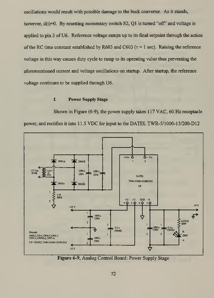
oscillations would result with possible damage to the buck converter. As it stands,
however, d(t)=0. By resetting momentary switch S2, Ql is turned "off' and voltage is
applied to pin 3 of U6. Reference voltage ramps up to its final setpoint through the action
of the RC time constant established by R603 and C603 (x = 1 sec). Raising the reference
voltage in this way causes duty cycle to ramp to its operating value thus preventing the
aforementioned current and voltage oscillations on startup. After startup, the reference
voltage continues to be supplied through U6.
f. Power Supply Stage
Shown in Figure (6-9), the power supply takes 117 VAC, 60 Hz receptacle
power, and rectifies it into 1 1.5 VDC for input to the DATEL TWR-5/1000-15/200-D12
117 Vac60 Hz
D901A
D902A
D901B
lOOOu
C901 :
D902B
1000 u,
C902'
IMR902
+15 V
O O - Vin+V.n O1 2
DATEL
TWR-5/100M5/200-D12
W
+15 -15 GND +5
4Q SO 6Q ?Q
Grounds
R902-2, U9-6, C904-2, C905-
1
C907-2, C907G-2, D907-A
U9 = DATEL TWR-5/1000-15/200-D12
1000 u
C904
1000 u
C905
f
01 u
C904D
+5V
. 1000 u
*C907
**• 0.510 KR907
-0 1 u
'C907G
<§kK
D907
A
Figure 6-9, Analog Control Board: Power Supply Stage
72

voltage regulator. The output of the DATEL module is +5 VDC and +13.5 V^ supply
power for the control board. The +15 V^ is not obtained due to minimal circuit loading.
The lower +13.5 VDC values meet control board component power supply requirements.
4. IGBT Driver Board
The IGBT driver board completes the feedback loop. Input to the board can be
made using twisted pair (analog control) or optical interface (digital control). Both
configurations are shown in Figure (6-10). The input driver signal is amplified to + 10 V
by the optically isolated push-pull transistor pair in Ul . Following amplification, the
driver signal is applied to the IGBT gate. The back-to-back 1N4744 zener diodes (Vz= 15
V) were installed across the gate to prevent overvoltage damage.
117 Vac60 Hz
14 Vet
1N400S
D108A
1N4005
D104A
1N4005
D108B
1N400S
D104B
•2200u' C108
If
2200 u
C104
+10.9 V
-o
0.22 u
C148
-10.9 V
H0.9VLM7WIBACZ
VR1
2+5V
I
2
0.1 u^ C203
['
t
Grounds
C104-1, C108-2, VR1-3, C203-2
DGATE1-A, U2-2
U1=TLP250
U2 = HFBR-2521
Note: For optical interface, R201 = 510 K.
For twisted pair interface, remove VR1 , U2, and C203
Connect the twisted pairtoTWl+' and TW1-' Size R201 for 8 mAof current R201 = 1.3 K if the input pulses are +/- 13 V.
+5V/D#-TW+
Figure 6-10, IGBT Driver Board
73

5. Digital Control Board
Reference [7] contains a detailed description on the layout and operation of the
Load Buck Converter digital control board.
74

VII. CONCLUSIONS
This research documented the design of SSCM units and their controllers for the
PEBB Network Simulation Testbed being built at the Naval Postgraduate School. In
addition, baseline simulations were developed to identify system instabilities and
interesting controller interactions. Finally, hardware validation studies were conducted to
confirm the PEBB Network simulations.
The SSCM design process began with the selection of components for the buck
converter power sections. The initial selections were based upon system specifications,
theoretical calculations, and physical limitations. The process continued with the
development of state-difference analog and digital control algorithms. Next, gain
selection was performed for the Source Buck Converter analog controller and the Load
Buck Converter digital controller. Chapter IV showed that to achieve the desired
response, proper output capacitor sizing and current gain selection had to be achieved to
minimize unwanted harmonic effects in the system output.
With the proper gain values determined, detailed ACSL simulations were
performed as described in Chapter V. The results showed that the PEBB Network is
stable under the seven basic operational modes. In addition, hardware validation studies
were conducted for Modes 1, 4 and 5. The results of this testing verified that the ACSL
simulations correlated well with hardware implementation. From this process, it was
shown that the SSCM units operated to their design specifications.
75

One issue not considered in the initial design process, however, dealt with
shielding. As shown in Chapter V, switching noise had a considerable effect on the
system. This problem will only grow worse with the addition ofmore SSCM and SSIM
units. As a result, the next generation of SSCMs need to employ methods to eliminate
switching noise. Several recommendations include:
• soft switching
• placement of an enclosure about the buck converter power sections
• relocation of the buck converter controllers to a separate enclosure
• use of fiberoptic connections between controllers and feedback paths.
An additional system improvement deals with the replacement of the Source Buck analog
controllers with digital controllers. This step will greatly enhance the flexibility of the
PEBB Network since frequency and gain modifications can be performed in software for
the digital controller. As a result, a wide variety of system interactions can be
investigated "on the fly" rather than having to wait for resistor replacements on the
analog control boards. In addition, the digital control provides another layer of noise
immumty.
Recommendations for future research focus on further development of the ACSL
simulation models. Areas for investigation include:
• effect of buck converters operating at different frequencies
• implementation of an ARCP synchronous reference frame current controller
• incorporation of Gaussian white noise into the sensed variables to model the
effects of switching noise.
76

Ideally, these detailed simulations can then be used to direct hardware testing towards
interesting PEBB Network interactions and stability bounds.
77

78

APPENDIX A. DATASHEETS
A. INTERNATIONAL RECTIFIER IRGT1090U06 IGBT
Internationaltor]Rectifier
PD-9.954B
IRGTI090U06"HALF-BRIDGE" IGBT INT-A-PAK
•Rugged Design•Simple gate-drive
•Ultra-fast operation up to 25KHz hardswitching, or 1 0OKHz resonant•Switching-Loss Rating includes all "tail"
losses
Description
IR's advanced IGBT technology is the key to
this line of INT-A-pak Power Modules. Theefficient geometry and unique processing of
the IGBT allow higher current densities than
comparable bipolar power module transistors,
while at the same time requiring the simpler
gate-drive ofthe familiarpowerMOSFET. This
superior technology has now been coupled to
state of the art assembly techniques to pro-
duce a higher current module that is highly
suited to power applications such as motor
drives, uninterruptible power supplies, weld-
ing, induction heating and ultrasonics.
Ultra-fast™ Speed IGBTHalf-Bridge
V^ = 600V
lc= 90A
VCE(ON)<3.0V
INT-A-PAK case
Absolute Maximum Ratings
Parameter j Description Value Units
VCES |
Continuous collector to emitter voltage 600 V
lc9Tc = 25'C I Continuous collector current 90
A
l c ® T c = 85' C | Continuous collector current 60
lc Tc = 100°C I Continuous collector current 50
>LU Peak switching current 180
In Peak diode forward current ( 1 ) 225
VGE |Gate to emitter voltage ±20
VV.SOL RMS isolation voltage, any terminal to case, t= 1 min 2500
P 9TC = 25"C Power dissipation 298 WTj Operating junction temperature range -4010 150
°CTST<3 Storage temperature range -40 to 125
(1) Duration limited by max junction temperature.
79

IRGTI090U06 I©R
Electrical Characteristics - T. = 25SC, unless otherwise stated
Parameter Description Mm Typ Max Units Test Conditions
BVC„ Collector-to -emitter breakdown voltage 600 — -
V
VQE - 0V, lc = 1 mA
VCE(ON) Collector-to -emitter voltage — — 3.0 VCE = 15V.lci 90A
— 3.1 — Vqe = ISV.Ic = 90A,Tj = 1 50°C
VFM Diode forward voltage- maximum — — 2.8 l F=» 80A. Vqe = 0V
— 2.6 — l,.=90A,VGE =0V,TJ= 15O'C
Van Gate threshold voltage 3.0 - 55 l
c= 500uA
AVooh Threshold voltage temperature coetf. — -11 — mWC V^V^t-SOBHAhi Forward transconductance 34 — 58 S(O) VCE = 25V.IC=90A
Ices Coliector-to-emitter leakage current — — 1
mAVGE = OV.VM = 600V
— — 10 va^ov,vCE=eoov.TJ=i5o,c
'qes Gate-to-emitterleakage current - - ±1 uA VQE = ±20V
Dynamic Characteristics - Tj 150°C
Parameter Description Mln Typ Max Units Test Conditions
*-on Turn-on switching energy — 0.05 - Ra,=470^ = 00
E 0(t d) Turn-off switching energy — 0.05 — mJ/A l
c= 90A.Ls =100nH
E„ 0> Total switching energy — — 0.12 VGC=360V,VQE = *15V
Wl Tum-on delay time — 70 - R01 .47n.R<B =ont, Rise time — 90 —
lc .90A
Wrf) Turn-off delay time — 180 — VCC =360V.V0E = *15V
«lFall time — 250 — Lj=100nH
•rr Diode peak recovery current — 52 — A R,= 470^=00
t,r Diode recovery time — 110 — ns lc= 90A
Qrr Diode recovery charge — 3.0 — uC VCC=360V.VG6 -±1SV
Q„. Gate-to-emlttercharge (tum-on) 150 — 280 VCC = 360V
Q9c
Gate-to-collector charge (tum-on) 70 — 140 nC l
c = 90A
Q Total gate charge (tum-on) 26 — 42 Vqe=15V
cta Input capacitance — 5800 — Voe = ov
c^ Output capacitance — 660 — PF VCC = 30V
Cres Reverse transfer capacitance — 80 - fxIMHz
( 1 ) Includes tail losses
Thermal and Mechanical Characteristics
Parameter Description Typ Max Units
Rwc (IGBT) Thermai resistance, junction to case , each IGBT — 0.42
•CrWRmjc (Diode) Thermal resistance , junction to case , each diode — 0.7
R,,^ (Module) Thermal resistance . case to sink 0.1 -Wt Weight of module 140 — g
80

IOR IRGTI090U06
1QDD ICED
Fig. 1 - Typical Output Characteristics. T, - 25°C
2 A 6 8 10
V^.Cclectcr^o€rrmer VtttccjB (V)
Fig. 2 - Typical Output Characteristics, T, = 150°C
jS| I ! I I I
i
-m i_4DOBPUto \Mc*h f
| ,KU1
-
I I
I 1/ ! // '/
I
/"/
/A >
j |
; 1
I |
i '1 1
, >3ZJ—I—,—!—I—i
—
: 1 1 i
1.5 26 3L5
tatci iH-iwOLaForwcrdVtofrQOPCV)
Fig. 3 - Typical Output Characteristics
5 10 15 20
V<SE
Gc*s-1o€mtter Vfartaas CV>
Fig. 4 - Typical Transfer Characteristics
ISO
T . JunctionTemperartrorO
Fig. 5 - CoUector-to-Emitter Saturation
Typical Voltage vs. Junction Temperature
1201—
I
i
1101—
T
J-2S'C,100—
T
Jr ia70
90
1 1.5 2 25 3 15 4
InstcrstaneoLE Favsarrd Voltage (V)
Fig. 6 - Forward Voltage Drop Characteristics
81

IRGTI090U06 IOR
IO 1
'
1!
1'
; 1
14 _I C -54A j
/':\
I j
1 ' !! 1
! 1 !1
.
| ! !|
i
i
| ;
a- ' !
!
t /'
|
i
6/I
1 __i1
1
I
B / ! i i
i
!i
; I, i i
40 80 120 \(D 200 240
G^. Tofc* Gate a-croo CrO
Fig. 7 • Typical Gate Charge vs.
Gats-to-Emlttar Voltage
8
LyyaacMIK© -47 oh
1
nn «cr*^
j- l
i^-^!
i 34A^«
i ---^1 17A
^^-^—!
"
, ii
i
25 3D 75 10D 125 133
Tj, Juncflcn t« i pflfldue) C°CD
Rg. 9 - Typical Switching Losses
vs. Junction Temperature
8,
UaMM j j
: >1p/ J
! 1 ^^• 15LTV. | V-
! CI
yr i
C1
i
1
jS i
X\ ij/| i
3 1 ' "1
1' '
- 1
10 30 SO 70 SO 110 130 ISO 170
I?G Gate raseWcncs (arm)
Fig. 1 1 - Typical Switching Lossesvs. Gate Resistance
V^. C3dtecror-to€rr«»erVUraoe (NO
Fig. 8 - Typical Capacitance vs.
CoHector-to-Emltter Voltage
f1
V^ -*15VVQJ.-340V
i j/\
1
*i
1/ !
20 40 100
Ic . Cctector-toEmfrrer Ourent (A)
Fig. 10 - Typical Switching Losses vs.
Collecior-tc-Emltter Current
1000
100 200 300 4DD 500 600 700
VCE .rvtoajjeclcrT»rriraBC/i
Rg. 12 - Reverse Bias Sate Operating Area
82

IOR IRGTI090U06
Ql
1001 1 i
1 11 r :
<aa I1
|
i
j :1 ! 9r0mtma
L_ MOV»
80 1I
' £\jc1
| J-L , p~>^ ..c v
±;i70i
'J^ l^j-V,
«1 1
' >^ ,f.i
60
40
30
Hi j—- ^ '
—-^ J\!
|
i ' I2spc : 1 ^-^ ' v v '
1 Mill _i«rw- ! 1 7-1^ lV^K^
(p -Q« nod (load crew* l T^ i^ V2D ! 1 .
"^ N >rn»aa0(moajcnoncBp
JaJvdtan ••
» Fundomentda oe '
1"*S* J
80% of mot., H— 1
'11
r^-r-l———— -^
10D1 10
MaajotlngftooiJBncv.fCKHO
Fig. 13 - Typical RMS Output Current per phase vs. Frequency (Synthesized Sinusoidal Wave)
1 1 ™~\
120
vr1
Tpr^6
100_RG -47 err
_LS -WOr*VCC" 360V
n i
H !
| I
SO,
401 *—— | j !
1
'BR 3
4D+*^^ • —y.—i
;
i
';
2DI
i ' tt/ra
1
'
"11 i 1 1 1
•
n20 40 CO 83 ICO ISO 14D MO
PeckOJpLf CXrrarr. IqO*>
Rg. 14 - Typical Diode Recovery Characteristics as Function of Output Current lQ
t, . naetonoJcrRt»rxroticnGeo
Rg. IS - Maximum Effective Transient Thermal Impedance. Junction-to-Case
83

IRGTI090U06 IOR
^ -V Vvi—
J
"ZT—
,w •-Vjg = 360V
Ls =(L, Lj* L3) = lOOnH
L = ImHV„ = * 15V
HQ. 1 6 - Test Circuit for Measurement of l^, E^. E^ Q^,. !„,.i^ V *ogim . t,
rr;; . , . L ... ..V VQ fc^Si^" 1 ~* J Oev.ce j*c*e» Tea
tvqe
_LilHCu«W( n iGBT
Cuffer.t in
APeverre voiloge fceranf'eew-ee Diooe
E«l( -. '. : 4t
?--V
Fig. 17 - Test Waveforms tor Circuit of Fig. 16
Volte; e Ou:
*>CC! ••: *'.
./
Irr . -rr .-<
Fig. 18 - Test Waveforms tor Circuit of Fig. 16, Defining E^. E,^, tomH), tr, lRR , t^,. Q^,
84

B. UNITRODE UC3637 PWM DRIVER IC
DESCRIPTIONThe UC1637 is a pulse width modulator circuit intended to be used for a variety ofPWM motor
drive and amplifier applications requiring either uni-directional or bi-directional drive circuits.
When used to replace conventional drivers, this circuit can increase efficiency and reduce
component costs for many applications. All necessary circuitry is included to generate an analog
error signal and modulate two bi-directional pulse train outputs in proportion to the error signal
magnitude and polarity.
This monolithic device contains a sawtooth oscillator, error amplifier, and two PWMcomparators with ±100mA output stages as standard features. Protection circuitry includes
under-voltage lockout, pulse-by-pulse current limiting, and a shutdown port with a 2.5V
temperature compensated threshold.
The UC1637 is characterized for operation over the full military temperature range of -55°C to
+125°C, while the UC2637 and UC3637 are characterized for -25°C to +85°C and 0°C to +70°C,
respectively.
ABSOLUTE MAXIMUM RATINGS (Note 1)
Supply Voltage (±Vs) ±20VOutput Current, Source/Sink (Pins 4, 7) 500mAAnalog Inputs (Pins 1, 2, 3, 8, 9, 10, 1 1 12, 13, 14, 15, 16) ±VsError Amplifier Output Current (Pin 17) ±20mAOscillator Charging Current (Pin 18) -2mAPower Dissipation at TA = 25°C (Note 2) lOOOmWPower Dissipation at TC = 25°C (Note 2) 2000mWStorage Temperature Range -65CC to +150°C
Lead Temperature (Soldering, 10 Seconds) +300°C
Note J: Currents are positive into, negative out ofthe specified terminal.
Note 2: Consult Packaging Section ofDatabookfor thermal limitations and considerations ofpackage.
BLOCK DIAGRAM
+v*Sr-
+A» -AIM
m M
+VTH[TJ
UNDEfl-VOLTAOELOCKOUT
-Hoik
Qi«<i
„ ERROR-V!»[|]—
^vj rr^=HS SHUTDOWN
8HUToowr
m
COUP
-^-—:^<^^1*-
SQ ZOOmY^<tZJBowr
-H-C/L
-@+C/L
B/A OCTfLTEllBm i-HM
Hvti: PbuK litehM irn r»f«t donilnant
«96
85

CONNECTION DIAGRAMDH--18(TOPVIEW)JorN Package
orEE
VmQ
§IMT
MrQ i«aM
9 BBm9-OA
*»[£ |t«A
taaQ !|«ab
Ml ^M>
SOIC-20 (TOP VIEW)fJW Package
4VTWQ
org
-vthE
w
a OUTPHY
g*»MurB
v»gunrB
B*EM
B+6A.
D«ah]-ji»i
INK
PLCC-20, LCC-20(TOP VIEW)Q, L Packages
/ 8 2 1 2018
4O
1ft
5
8
7
88 10 11 12 13
PACKAGE PMFUNCTION
FUNCTION PIN
VTH 1
CT 2
-VTM 3
AirtJT 4
-VS S
wc 6
+Vs 7
Bout 8
1-BlN 9
-Bin 10
-A in 11
AlN 12
*CVL 13
C/L 14
SHLTTOOWN 15
WC 16
*E/A 17
-E/A IS
E'AOUTPUT 19
ISET 20
ELECTRICAL CHARACTERISTICS:Unless otherwise stated, these specifications apply for TA = -55°C to +125°C for the UC1637; -25°C to
+85°C for the UC2637; and 0°C to +70°C for the UC3637; +VS =+15V, -VS = - 15V, +VTH = 5V, -VTH= -5V, RT = 16.7kW, CT = 1500pF, TA=TJ.
PARAMETER TEST CONDITIONS UC1637/UC2637 UC3637 UMTSmm TYP | MAX MM TYP MAX
OwflWnr
Initial Accuracy Tj=25°C(Note6) 9.4 10 10.6 9 10 11 kHz
Voltage Stafcfflty Vs =±SVto ±20V, VPin i =3V.VP1N3 = -3V
5 7 5 . 7 %
Temperature StatOBy Over Operafing Range (rvote 3) 0.5 2 05 2 %+Vth Input Bias Current VPIN2=6V -10 0.1 to -10 0.1 10 uA
-Vth Input Bos Current VP1N2=0V -10 -0.5 -10 0.5 PA
Vth. -Vth Input Range *VS-2 -Vs+2 +VS-2 -VS+-2 V
Error Amplifier
input Offset Voltage Vcw-OV 15 5 1.5 10 mVinput Bias Current Vcw = QV 0,5 5 05 5 UA.
Inpul Offset Current VCMsOV 0.1 1 0.1 1 JtA
Common Mode Range Vs -.12.5 to 20V -Vs*2 -Vs -Vs*2 Vs V
Open Loop Voltage Gain Rl - 10k 75 100 80 100 dB
Stew Rate 15 15 V^is
Unity Gain Bandwidth 2 2 MHz
CMRR Over Common Mode Range 75 100 75 100 dB
PSRR Vs-.i2-5to±20V 75 110 75 110 dB
86

ELECTRICAL CHARACTERISTICS:Unless otherwise stated, these specifications apply for TA = -55°C to +125°C for the UC1637; -25°C to
+85°C for the UC2637; and 0°C to +70°C for the UC3637: VS =+15V, -VS - - 15V, +VTH = 5V, -VTH =
-5V, RT = 16.7kW, CT = 1500pF, TA=TJ.
PARAMETERS TEST CONDITIONS UC1637/UC2637 UC3S37 UMTS
MM TYP MAX MM TYP MAXError AmpSf tor (Ccntlrxwd)
Output Sink Current Vpw 17 * OV -50 -20 -50 -20 mAOutput Source Current VPW17-0V S 11 5 11 mA
High Level Output voltage 13 13.6 13 13.6 V
Low Level Output Voltage -14.8 -13 -14.8 -13 V
PWM Comparators
Input Offset Vottage Vcm • OV 20 20 rnV
Input Bias Current Vcm =W 2 10 2 10 uA
Input Hysteress VCM-OV 10 10 mVCommon Mode range Vs.±SVt0 220V -Vs+1 t-Vs-2 -Vs*1 »Vs-2 V
Current Limit
Input Offset Voltage Vcm = OV.Tj = 25'C 190 200 210 180 200 220 mVInput Offset Vottage T.C.
Input Bias Current
02 -0.2 mWC-10 -1.5 -10 •1.5 uA
Common Mode Range Vs=±2J5Vto±20V -Vs +VS-3 -Vs +VS-3 V
Shutdown
Shutdown Threshold (Note 4} -23 -2.5 •2.7 -2.3 -2.5 -2.7 V
Hysteresis 40 40 mVInput Bias Current VPWl4 = ~VStD-VS -10 -0.5 -10 -0.5 uA
Under-Vottage Lockout
Start Threshold (Note 5) 4.15 5.0 4.15 5.0 V
Hysteresis 0.25 0.25 mVTotaJ Standby Current
Supply Curosnl 85 15 8.5 15 mA
Output Section
Output Low Law) ISNK = 20mA -14.9 -13 -14.9 -13 V
|S4NK = 100mA 14.5 -13 -145 -13
Output High Levet Isource = 20mA 13 13.5 13 13.5 V
Isowoe = 100mA 12 13.5 12 13.5
Rise Time (MotB3>Cl-lnf,Tj-25'C ten £00 10D 600 ns
FalTime (l*t»3)a= Inf. Tj=25^ 100 300 100 300 n$
Note 3: These parameters, although guaranteed over the recommended operating conditions, are not 100% tested
in production.
Note 4: Parameter measured with respect to + VS (Pin 6).
Note 5: Parameter measured at + VS (Pin 6) with respect to -VS (Pin 5).
Note 6: RT and CT referenced to Ground.
FUNCTIONAL DESCRIPTIONFollowing is a description of each of the functional blocks shown in the Block Diagram.
Oscillator
The oscillator consists of two comparators, a charging and discharging current source, a current
source set terminal, 1SET and a flip-flop. The upper and lower threshold of the oscillator
waveform is set externally by applying a voltage at pins +VTH and -VTH respectively. The
+VTH terminal voltage is buffered internally and also applied to the ISET terminal to develop
the capacitor charging current through RT. If RT is referenced to -VS as shown in Figure 1, both
the threshold voltage and charging current will vary proportionally to the supply differential, and
the oscillator frequency will remain constant. The triangle waveform oscillators frequency and
voltage amplitude is determined by the external components using the formulas given in Fig. 1
.
87

+Vth
I* -t*VniH-ttl
RtI*
8CT[(<tVrHH-rni)]
+VTH - (-v»> +\ M+iu+it* /
Wo-
Figure 1. Oscillator Setup
PWM ComparatorsTwo comparators are provided to perform pulse width modulation for each of the output drivers.
Inputs are uncommitted to allow maximum flexibility. The pulse width of the outputs A and B is
a function of the sign and amplitude of the error signal. A negative signal at Pin 10 and 8 will
lengthen the high state of output A and shorten the high state of output B. Likewise, a positive
error signal reverses the procedure. Typically, the oscillator waveform is compared against the
summation of the error signal and the level set on Pin 9 and 1 1
.
MODULATION SCHEMESCase A Zero Deadtime (Equal voltage on Pin 9 and Pin 1 1)
In this configuration, maximum holding torque or stiffness and position accuracy is achieved.
However, the power input into the motor is increased. Figure 3A shows this configuration.
Case B Small Deadtime (Voltage on Pin 9 > Pin 1 1)
A small differential voltage between Pin 9 and 1 1 provides the necessary time delay to reduce
the chances of momentary short circuit in the output stage during transitions, especially where
power-amplifiers are used. Refer to Figure 3B.
Case C Increased Deadtime and Deadband Mode (Voltage on Pin 9 > Pin 1 1)
With the reduction of stiffness and position accuracy, the power input into the motor around the
null point of the servo loop can be reduced or eliminated by widening the window of the
comparator circuit to a degree of acceptance. Where position accuracy and mechanical stiffness
is unimportant, deadband operation can be used. This is shown in Figure 3C.
+w
OflGLLATOfl. /V/V(P* I)
ERRORBIQNAL(PIN 17)
UCM37
igure 2. Comparator Biasing
88

Output Drivers
Each output driver is capable of both sourcing and sinking 100mA steady state and up to 500mAon a pulsed basis for rapid switching of either POWERFET or bipolar transistors. Output levels
are typically -VS + 0.2V @50mA low level and +VS - 2.0V @50mA high level.
Error Amplifier
The error amplifier consists of a high slew rate (15V/ms) op-amp with a typical 1MHzbandwidth and low output impedance. Depending on the ±VS supply voltage, the common modeinput range and the voltage output swing is within 2V of the VS supply.
Under-Voltage Lockout
An under-voltage lockout circuit holds the outputs in the low state until a minimum of4V is
reached. At this point, all internal circuitry is functional and the output drivers are enabled. If
external circuitry requires a higher starting voltage, an over-riding voltage can be programmed
through the shutdown terminal as shown in Figure 4.
MM
w
2SZS2X Z:^^ "f^A,„J1—H—f1_ ^ !—!_i—U—
L
AOMT A»ur -uuuitH
Figure 3. MocWaton Sch«m«* Shoeing (A) Z«ro Dewjtirr* (B) DeadtSme and (C) Daadfoanel Conr^uratlons
Shutdown Comparator
The shutdown terminal may be used for implementing various shutdown and protection schemes.
By pulling the terminal more than 2.5V below VIN, the output drivers will be enabled. This can
be realized using an open collector gate or NPN transistor biased to either ground or the negative
supply. Since the threshold is temperature stabilized, the comparator can be used as an accurate
low voltage lockout (Figure 4) and/or delayed start as in Figure 5. In the shutdown mode the
outputs are held in the low state.
89

Vrrjmr -
UC16S7
Vt2.5V
2.3<R-URg)
Rl
TSHUTDOWN
:R2
-v«
Figure 4k Eaemal Under-Voltage Lockout Figure 5. Delayed Start-Op
Current Limit
A latched current limit amplifier with an internal 200mV offset is provided to allow pulse-by-
pulse current limiting. Differential inputs will accept common mode signals from -VS to within
3V of the +VS supply while providing excellent noise rejection. Figure 6 shows a typical current
sense circuit.
Figure 6. Cuirert Omit Sensing
90
«!4V
cipF
Figure 7. Bi-Oirectonai Motor Drive with Speed Contra) Power-AmpWier
«—i—
r
PDMTlONOOMUAMDVOLT/WB
=*}*+V» W BHUT-
DOWN
AM—*-<WV
ss
position rea«Aqic yqcTAqe
Figtir* S. Single Suppfy Position Servo Motor Drive
91

92
APPENDIX B. SIMULINK BLOCK DIAGRAMS AND MATLAB CODE
A. SOURCE BUCK CONVERTER
The Matlab m-files and Simulink block diagram used to generate first-cut gain
selections for the Source Buck Converter are provided below.
1. Matlab M-file buckcons.m
0^**********4
% buckcons.m
%% Specifications:
%% 90 A IGBTs% Analog controller patterned after SSCM.%% Want continuous operations between 10% and
% 100% loading.
%% Simulation sequence cycles through
% startup -> 10% loading -> full loading.
%% Written by: Mike Badorf
% Last mod: 2JUN97%************************************************
O^* ******************* ****************************
% Constant Definitions
% input voltage ofbuck
% desired output voltage of buck: 10%% output power
% chosen based on fres« fline & parts
% actual filter inductance value
% actual filter capacitance value
% low R value - full load current
% high R value - 10% load current
% starting resistance
% duty cycle
% 360 Hz ripple from 6 pulse rectifier
% switching frequency
% switching period
% pulse width for switching noise SS model
% actual inductance value for buck 1
93
E = 400.0;
Vcd = 305.0;
Pout = 9e3;
Cf = 400e-6;
Lfilt = 0.425e-3;
Cfilt = 2000e-6;
rx_full = 9.68;
rxten = 96.8;
rxstart = rx_ten;
d = Vcd/E;
fline = 360.0;
f = 20e3;
T = l/f;
pw = d*T;
L = 0.760e-3;
% Determination of Lcrit: low load R determineso^**************************************
R = rx ten;
Lcrit = (T*R/2)*(l-d); % critical inductance
K«
% Determination of delta I, Imax, Imin, ILavg
% and IJoad at 10% load (11).
0/ ************************************************
deltaj = ((E - Vcd)/L)*d*T;
Imaxjl = d*E*(l/R + (l-d)*T/(2*L)); % 11 max L current
Iminjl =d*E*(l/R-(l-d)*T/(2*L)); % 11 min L current
ILavg 11 = (Imax_ll+Imin_ll)/2; % 11 avg L current
IJoad ll = Vcd/R; % 11 current
K«
% Determination of Imax, Imin, ILavg
% and IJoad at full load (fl).
R = rx_full;
Imax = d*E*(l/R + (l-d)*T/(2*L)); % fl max L current
Imin =d*E*(l/R-(l-d)*T/(2*L)); % fl min L current
ILavg = (Imax+Imin)/2; % fl avg L current
IJoad = Vcd/R; % fl current
o/o************************************************
% Determination of resonant peak for L / Cf LPF.o/ ****** ****************************** ************
fres = l/(2*pi*sqrt(L*Cf));
0/q* ***************************************** ******
% Determination of resonant peak for
% input Lfilt / Cfilt LPF.0/ ******************
:
fres_filt = l/(2*pi*sqrt(Lfilt*Cfilt));
94

2. Matlab M-file buckstrt.m
% buckstrt.m
%% Provides startup parameters for 9 kW, 20 kHz% buck chopper.
%% Calls buckcons.m, a constant file developed
% for above buck chopper.
%% Written by: Mike Badorf
% Last mod: 2JUN97
clear % clear MATLAB memorybuckcons % establish buck constants
o/ *** ******************************* **************
% Bessel Pole specifications
wo = 3250;
poles = wo*[ -0.942 -0.74550+0.71 12*i -0.7455-0.71 12*i];
% desired characteristic polynomial used to
% determine gains
S = poly(poles);
Yo*
% Gain calculations: Calculated using low
% starting resistance. Gains are utilized as
% first run starting point. Entry ofmanual
% gains can follow to give best overall
% response over all operating conditions. Use
% board resistors in practice to set gains.
0/ ************************************************
R =rxstart;
hi = ((L*R*Cf*S(2))-L)/(E*R*Cf)
hn = (L*Cf*S(4))/E + hi*L/2
hv = ((L*R*Cf*S(3))-(E*hi)-R)/(E*R)
Vo*
% Function to verify poles obtained with gains
% match desired poles.
ty ************************************************
Am = [0 -1/L E/L
1/Cf -l/(R*Cf)
-hv/Cf (hi/L)+(hv/(R*Cf))-hn -hi*E/L ];
95

closedsyspole = eig(Am) % check for correct poles
0/ * ***********************************************
% SIMULINK no load parameters (are in addition
% to constants determined in buckcons.m)
% ABCD state space parameters
A = [-l/(R*Cf) 1/Cf
-1/L ];
B = [0
E/L];
C = [l
1];
D = [0
0];
% Update initial conditions for integrators
0^******** ****************************** **********
Vciv - 304;
iLiv = Vciv/R;
hnintiv = 0.0;
dutyiv =304/E;
tstart =0.0;
tstop =0.012;
% initial Vc integrator value
% initial hn integrator value
% initial hn integrator value
% initial duty cycle value
% simulation start time
% simulation stop time
96

3. Matlab M-file buckfull.m
w% buckfull.m
%% Provides full load parameters for 9 kW,% 20 kHz buck chopper.
%% Written by: Mike Badorf
% Last mod: 2JUN970,^************************************************
R = rxfull; % full load resistance value
0/Q* ***********************************************
% Function to verify poles obtained with gains
% match desired poles.
0/ ************************************************
Am = [ -1/L E/L
1/Cf -l/(R*Cf)
-hv/Cf (hi/L)+(hv/(R*Cf))-hn -hi*E/L ];
syspole = eig(Am); % check for correct poles
0/Q**** ******************************* *************
% SIMULINK no load parameters (are in addition
% to constants determined in buckcons.m)
% ABCD state space parameters
A = [-l/(R*Cf) 1/Cf; -1/L ]; B =[ 0; E/L];
C = [10; 01];D = [0; 0];
% Data passdown before buckfull.m simulation
% begins.
0/ ************************************************
Vc_response = Vc;
iL_response = iL;
dutyresponse = duty;
timer = time;
Vo*
% Update initial conditions for integrators in
% buckfull.m simulation.
o/ * ***************************** ******************
Vciv = Vc(length(time)); % Vc initial value for buckfull.m
iLiv = iL(length(time)); % iL initial value for buckfull.m
dutyiv = duty(length(time)); % duty initial value for buckfull.m
tstart = tstop; % sim. start time for buckfull.m
tstop = tstop + 0.012; % simulation stop time for buckfull.m
97

4. Matlab M-file buckten.m
0/^************ ************** **********************
% buckten.m
%% Provides 10% load parameters for 9 kW, 20 kHz
% buck chopper.
%% Written by: Mike Badorf
% Last mod: 2JUN97
R = rxten; % 10% load resistance value
0/ ************************************************
% Function to verify poles obtained with gains
% match desired poles.
0/ ************************************************
Am = [ -1/L E/L
1/Cf -l/(R*Cf)
-hv/Cf (hi/L)+(hv/(R*Cf))-hn -hi*E/L];
syspole = eig(Am); % check for correct poles
% SIMULINK no load parameters (are in addition
% to constants determined in buckcons.m)
% ABCD state space parameters
A = [-l/(R*Cf) 1/Cf; -1/L ]; B =[ 0; E/L];
C = [10; 1];D = [0; 0];
o,- ** **************************** ******************
% Data passdown before buckten.m simulation
% begins.
o^** **************************** ******************
Vc_response = [ Vcresponse; Vc];
iLresponse = [ iLresponse; iL];
dutyresponse = [ dutyresponse; duty];
timer = [ timer; time];
o/ * ***********************************************
% Update initial conditions for integrators for
% buckten.m simulation.
o/ * ********************************************** *
Vciv = Vc(length(time)); % Vc initial value for buckten.m
iLiv = iL(length(time)); % iL initial value for buckten.m
dutyiv = duty(length(time)); % duty initial value for buckten.m
tstart = tstop; % simulation start time for buckten.m
tstop = tstop + 0.012; % simulation stop time for buckten.m
98

5. Matlab M-file buckplot.m
70
0,Vo buckplot.m
%% Plot startup, change to 100% loading, &% change to 10% loading for 9 kW, 20 kHz buck
% chopper.
%% Written by: MikeBadorf
% Last mod: 21SEP96%******* ********************************** *******
Vc_response = [ Vc_response; Vc ];
iLresponse = [ iLresponse; iL ];
duty_response = [ dutyresponse; duty];
timer = 1000*[ timer; time ];
datastep =1:1 :length(timer); % Allows plotting fewer points
% than generated.
figure(l)
subplot(3,l,l), plot(timer(datastep), Vc_response(datastep),'b'), grid
title('Vc Response'),ylabel('Vc (volts)')
subplot(3,l,2), plot(timer(datastep), iL_response(datastep),'b'), grid
title('iL Response'),ylabel('iL (amps)')
subplot(3,l,3), plot(timer(datastep), 10*duty_response(datastep),'b'), grid
title('d(t) Response'),xlabel('time (msec)'),ylabel('10*d(t)')
99

6. Simulink Block Diagram
'. :
—
"
7T7T:
.
". '":- ',""''""" _____—. __
H
T*
______Pi
Ti
I
E
Figure B-l, Source Buck Converter Simulink Block Diagram
100

B. LOAD BUCK CONVERTER
The Matlab m-file, buckcons.m, and the Simulink block diagram for the Load
Buck Converter are provided below. The remaining m-files are provided above since the
transient response generation is the same for both the Source and Load Buck Converters.
1. Matlab M-file buckcons.m
% buckcons.m
%% Determining Buck Circuit Parameters
%% Specifications:
%% 90 A IGBTs% Analog controller patterned after SSCM.%% Want continuous operations between 10% and
% 100% loading.
%% Simulation sequence cycles through
% startup -> 10% loading -> full loading.
%% Written by: Mike Badorf
% Last mod: 21SEP960/ ********* ******************************** *******
% Constant Definitions
% input voltage of buck
% desired output voltage ofbuck
% output power
% chosen based on fres« fline & parts
% actual filter inductance value
% actual filter capacitance value
% low R value - full load current
% high R value - 10% load current
% starting resistance
% duty cycle
% 360 Hz ripple from 6 pulse rectifier
% switching frequency
% switching period
% pulse width for switching noise SS model
% actual inductance value for buck
E = 300.0;
Vcd = 208.0;
Pout = 3e3;
Cf = 400e-6;
Lfilt = 0.425e-3;
Cfilt
rxjull
= 460e-6;
= VcdA2/Pout:
rx_ten = 10*rx_full;
rxstart
d
= rx ten;
= Vcd/E;
fline = 360.0;
f = 20e3;
TpwL
= l/f;
= d*T;
= 1.3e-3;
101

% Determination of Lcrit: low load R determines0/ ************************************* *
R = rx ten;
Lcrit = (T*R/2)*( 1 -d); % critical inductance
% Determination of delta I, Imax, Imin, ILavg
% and IJoad at 10% load (11).
q/Q*** ******************************** *************
deltaj = ((E - Vcd)/L)*d*T;
Imaxjl = d*E*(l/R + (l-d)*T/(2*L)); % 11 max L current
Iminjl =d*E*(l/R-(l-d)*T/(2*L)); % 11 min L current
ILavgJl = (Imax_ll+Imin_ll)/2; % 11 avg L current
I load ll = Vcd/R; % 11 current
% Determination of Imax, Imin, ILavg
% and IJoad at full load (fl).
Vo*
R = rx_full;
Imax - d*E*(l/R + (l-d)*T/(2*L)); % fl max L current
Imin =d*E*(l/R-(l-d)*T/(2*L)); % fl min L current
ILavg = (Imax+Imin)/2; % fl avg L current
IJoad - Vcd/R; % fl current
q^** ******** ****************************** ********
% Determination of resonant peak for L / Cf LPF.q,^******* ************ *****************************
fires = l/(2*pi*sqrt(L*Cf));
q,^***************************** *******************
% Determination of resonant peak for
% input Lfilt / Cfilt LPF.
q/ ************************************************
fresjllt = l/(2*pi*sqrt(Lfilt*Cfilt));
102

2. Simulink Block Diagram
Figure B-2, Load Buck Converter Simulink Block Diagram
103

104

APPENDIX C. ACSL CODE
A. SOURCE BUCK CONVERTER GAIN SELECTION CODE
The computer code for this section is comprised of the main ACSL program, two
supporting macro files and the command file used to generate transient load studies.
1. Main Program
sourcebuck.csl
This program simulates the operation of a 9 kW source buck converter unit operating at
20 kHz assuming ideal components and no line losses. The converter has been designed
to operate as follows:
400 Vdc input voltage
300 Vdc nominal output voltage
continuous ind. current from 10% -> 100% load
The controller for this simulation makes use of the analog control algorithm derived
in Chapter III. The file, sourcebuck.cmd, contains the runtime commands utilized to
exercise this model.
Written by: Michael Badorf
Last modified: 02JUN97
INCLUDE 'buck.mac*
INCLUDE 'analogcontrol.mac'
PROGRAM sourcebuck
INITIAL
MAXTERVAL maxt = 1 .0e-6 ! "maximum integration step size"
MINTERVAL mint = 1.0e-8 ! "minimum integration step size"
! "for variable step algorithms"
CINTERVAL cint = 1 .Oe-6 ! "data communication interval"
ALGORITHM ialg = 5 ! "integration algorithm"
!"4-RK.2nd, 5--R.K. 4th"
NSTEPS nstp = 1
CONSTANT tstop = 1 .0 ! "stop point for integration
CONSTANT Vramppk= 10.0 !"pk value of ramp modulating waveform "
CONSTANT swfreql = 20000.0 ! "switching frequency for buck 1
Tramp 1 = 1.0/swfreql ! "switching period for buck 1
END ! "of initial"
105

DYNAMIC
TERMT(t .GE. (tstop-0.5*cint))
DERIVATIVE
Vincap 1 = 400.0 ! "define a hard input voltage of 400 Vdc"
! source buck converter unit 1
tpwml = MOD(t,Trampl) !"time elapsed in switching period for buck 1
Vrampl = Vramppk*tpwml/Tramp 1 ! "establish ramp modulating waveform for buck 1"
! "implement source buck converter unit 1 macro"
buck( 1 ,Vincap 1 ,iout 1 ,isw 1 ,iL 1 ,Vc,Vramp 1 ,"Lbuck 1 =760.0e-6","Vdidrop 1 =2.0",&
"Vswdropl=2.0")
["implement source buck converter unit 1 multiloop control macro
analog_control(l,Vincapl,Vc,ioutl,iLl,"RCstartl=0.6","hil=0.015","hvl=0.017",&
"hn 1=26.09")
CONSTANT Cbuckl =400.0e-6
CONSTANT Vcic = 0.0
pVc = (iLl - ioutl)/Cbuckl
Vc = INTEG(pVc, Vcic)
"output capcitance"
"output voltage IC"
"output voltage state"
"output voltage "
CONSTANT Rout = 96.8 ! "source buck converter startup load"
!"10% load value
ioutl = Vc/Rout ! "load current"
! end source buck converter unit 1
END ! "of derivative"
END ! "of dynamic"
END ! "of program"
106

2. Buck Converter Macro
*************************************************************************************
buck.mac
This macro governs the conduction status of a buck converter switch and uses this
condition to develop inductor current utilizing the inductor equation of state.
Switch and diode losses are modeled as voltage drops. All other components are ideal.
The output inductor current is used in the main program to determine output capacitor
voltage. Although this step could be done in the macro, the current arrangement
allows modeling more complex PEBB network configurations.
Written by: Michael Badorf
Last modified: 02JUN97******************************************************************************
MACRO buck(z,vin,iout,isw,iL,Vc,rampwav,pLbuck,pVdidrop,pVswdrop)
INITIAL
CONSTANT pLbuck
CONSTANT pVdidrop
CONSTANT pVswdrop
! "assign the initial inductor current"
CONSTANT iLic&z = 0.0
! "define and initialize the switch conduction status"
LOGICAL SWl&zSW 1&z = .true. !"T s 1 conducts, F s 1 blocks"
END
! "determine conduction status of SW1"PROCEDURAL(SW 1&z,isw=rampwav,duty&z,iL)
! "charge inductor when duty GT reframp"
IF (duty&z .GT. rampwav) THEN
SWl&z=.true.
isw = iL
ELSE
SWl&z =.false,
isw = 0.0
ENDIF ! "end if (duty&z .GT. rampwav)
END ! "of procedural"
107

! "Given conduction status of SW1 , and whether continuous or not,
!" determine derivative of iL"
PROCEDURAL(piL«&z=SWl&z,vin,Vc,Vdidrop&z,iL,Vswdrop&z,Lbuck&z)
"—if SW1 gated, assume can conduct pos. current"
IF (SWl&z) THEN
contmode&z = .true.
piL&z = (vin-Vswdrop&z-Vc)/Lbuck&z
ELSE
IF (iL .GT. 0.0) THEN
! "if IGBT not gated but iL greater than zero"
!"the diode conducts and the inductor discharges"
piL&z = (-Vdidrop&z-Vc)/Lbuck&z
ELSE
! "if IGBT not gated and iL less than or equal"
!"to zero, the diode is off and the inductor"
! "current and derivative are zero"
piL&z = 0.0
ENDIF ! "end if (iL .GT. 0.0)"
ENDIF !"endif(SWl&z)"
END !"of procedural"
! "integrate the inductor state variable"
iL = BOUND(0.0, 100.0, LIMINT(piL&z, iLic&z, 0.0, 100.0))
MACRO END
108

3. Analog Controller Macro
********************************************************************************
analogcontrol.mac
This macro governs the analog control algorithm derived in Chapter III. In addition
overcurrent protection is provided to place the controller in pulse-by-pulse
operations if inductor current exceeds 67.5 amps.
Written by: Michael Badorf
Last modified: 02JUN97**********************************************************
MACRO analog_control(z,Vin,Vout,iout,iL,pRCstart,phi,phv,phn)
INITIAL
CONSTANT pRCstart
CONSTANT phi
CONSTANT phv
CONSTANT phn
! "assign internal macro constants"
CONSTANT Vthouseref&z = 305.0 !"top of housecurve"
CONSTANT houseslope&z = 3.0 ! "housecurve slope"
CONSTANT Vthouseic&z = 0.0
CONSTANT Vxic&z = 0.0
CONSTANT iLlimit&z = 67.5 !"max. ind. current before prot. action"
CONSTANT dutylow&z =0.0
CONSTANT minduty&z = 0.0
CONSTANT maxduty&z =10.0
CONSTANT scale&z = 10.0
END
pVthouse&z = (Vthouseref&z-Vthouse&z)/RCstart&z ! "reference voltage state
Vthouse&z = INTEG(pVthouse&z, Vthouseic&z) ! "reference voltage
"
vcref&z = Vthouse&z - iout/houseslope&z
pVx&z = Vout - vcref&z ! "voltage state difference "
Vx&z = INTEG(pVx&z, Vxic&z) ! "integral voltage state diff."
! "control algorithm for source buck converter controller"
dutyML&z = -hi&z*(iL-iout)-hv&z*pVx&z-hn&z*Vx&z+Vthouse&z/Vin
! "overcurrent protection for buck converter controller"
!" ifbuck converter 1 is operating, implement overcurrent protection"
IF (iL .GT. iLlimit&z) THENduty&z = dutylow&z ! "overcurrent"
ELSEduty&z = BOUND(minduty&z, maxduty&z, scale&z*dutyML&z)
ENDIF ! "end if (iL .GT. iLlimit&z)"
MACRO END
109

4. Command File
sourcebuck.cmd
This runtime command file exercises the simulation by executing load changes. In this
way the transient response of a source buck converter can be analyzed. The file
contains a study that allows a source buck converter to start up. The final values of
this startup are used as ICs for the transient analysis. In this way, the transient
analysis can be run over and over without having to execute a startup every time.
Written by: Michael Badorf
Last modified: 02JUN97
sstrplt = .t. !"one variable per x-axis "
s calplt = .f.
s devplt =1 !"1 for screen output"
!"5 for postscript
sppoplt=.f. !"true rotates plot 90 deg "
sxinspl = 6 ! "x-axis plot units
s weditg = .f. ! "false suppresses data write"
! "each time SCHEDULE occurs "
s nrwitg = .t. ! "true enables accumulation of data
"
!"after a CONTIN
s dpnplt =.f. !"no date on plots
! "determines which variables to plot"
prepare t,iLl,ioutl,Vc,dutyl
!"startup of source buck converter"
proced sourcestartup
! "source buck startup parameters"
s Rout = 96.8 !"10% load"
! "simulation parameters"
s ialg = 5
s maxt = 1 .Oe-6
s cint = 1 .0e-3
s tstop = 3.0
start
s cint = 1 .Oe-6
s tstop = 4.0
contin
end
SAVE /FILE='sourcestartup' /BINARY /STATES /ICS /EVENTS
110

!"single source buck converter transient operation"
proced trans
["initial conditions restoration source converter startup"
RESTORE /FILE='sourcestartup' /EVENTS
["reinitializes states to new ICs"
REINIT
["source buck parameters"
s Rout = 96.8 !"10%load"
["simulation parameters"
s ialg = 5
s maxt = 1 .Oe-7
s cint = 1 .Oe-6
s tstop = 0.04
start
!"10% -> 100% source buck converter load change"
sRout =9.68
s tstop = 0.08
contin
end
["100% -> 10% source buck converter load change"
s Rout = 96.8
s tstop =0.12
contin
splt=l
plot /color=0 /XTAG='(sec)' &dutyl &ioutl /TAG='(amps)' &Vc /TAG='(volts)'
111

B. LOAD BUCK CONVERTER GAIN SELECTION CODE
The computer code for this section is comprised of the main ACSL program and
the command file used to generate transient load studies. The buck macro is provided
above.
1. Main Program
*************************************************************************************
loadbuck.csl
This program simulates the operation of a 3 kW load buck converter unit operating at
20 kHz assuming ideal components and no line losses. The converter has been designed
to operate as follows:
300 Vdc input voltage
208 Vdc output voltage
continuous ind. current from 10% -> 100% load
The controller for this simulation makes use of the digital control algorithm derived
in Chapter III. The file, loadbuck.cmd, contains the runtime commands utilized to
exercise this model.
Written by: Michael Badorf
Last modified: 02JUN97******************************************************************************
INCLUDE 'buck.mac'
PROGRAM loadbuck
INITIAL
MAXTERVAL maxt = 1 .Oe-6 !"maximum integration step size"
MINTERVAL mint = 1 .Oe-8 ! "minimum integration step size"
!"for variable step algorithms"
! "data communication interval"
! "integration algorithm"
!"4-R.K. 2nd, 5--R.K. 4th"
CINTERVAL cint = 1.0e-6
ALGORITHM ialg = 5
NSTEPS nstp = 1
CONSTANT tstop= 1.0
LOGICAL reinitf
CONSTANT reinitf = .false.
!"stop point for integration"
112

! Initialization of digital controller values: if reinitializing from previous
! run, then this section is skipped by setting reinitf = .true, in the
! command file.
IF (reinitf) GO TO skipin
Vthouse_old = 0.0
Verrold = 0.0
Vintold = 0.0
count = 0.0
skipin..CONTINUE
END ! "of initial"
DYNAMIC
TERMT (t .GE. (tstop-0.5*cint))
DERIVATIVE
Vincap3 = 300.0 ! "define a hard input voltage of 300 Vdc"
! load buck converter unit 3
! "implement load buck converter unit 3 macro
buck(3,Vincap3,iout3,isw3,iL3,Vc3,count,"Lbuck3=1300.0e-6","Vdidrop3=2.0",&
"Vswdrop3=2.0")
CONSTANT Cbuck3 = 400.0e-6
CONSTANT Vcic3 =0.0
pVc3 = (iL3 - iout3)/Cbuck3
Vc3 - INTEG(pVc3, Vcic3)
CONSTANT Rout3 = 144.0
! "output capacitance of load buck
! "output voltage IC
! "output voltage state
! "output voltage
!"load buck converter startup load
!"10% load value
iout3 = Vc3/Rout3 !"load current"
! end load buck converter unit 3
! load buck converter unit 3 digital controller overcurrent protection
CONSTANT iLlimit3 = 50.0 ! "pulse-by-pulse inductor current limit
CONSTANT dutylow3 = 0.0 ! "lower admissible duty cycle limit
CONSTANT minduty3 = 0.0 ! "lower admissible duty cycle limit
CONSTANT maxduty3 = 475.0 ! "upper admissible duty cycle limit
CONSTANT scale3 =500.0 ! "duty between 0-500 counts
113

! "if load buck converter operating, implement overcurrent protection"
IF (iL3 .GT. iLlimit3) THEN
duty3 = dutylow3! "overcurrent"
ELSEduty3 = BOUND(minduty3, maxduty3, scale3*dutyML3)
ENDIF !"end if (iL3 .GT. iLlimit3)"
duty3p = duty3/scale3 ! "scales load buck duty cycle to -> 1 range"
! end load buck converter unit 3 digital controller overcurrent protection
END ! "of derivative"
! implement load buck converter digital controller
DISCRETE COUNTER
"interval statement causes controller to sample every tcount seconds"
"set tcount large if load buck is to be idle; when putting on line"
" reset tcount to 1 .Oe-7, the clock speed of the NSWC digital"
" controller -> perform reset in command file"
INTERVAL tcount = 1.0e-7
count = count + 1 ! "clock -> advances "
! "every 1.0e-7 seconds"
CONSTANT Vthouseref3 = 208.0 ! "top of house curve"
! "reference voltage with startup "time constant" of 0.06 sec"
Vthouse3 = Vthouse_old + 700*tcount
! "memory for old reference voltage value - used on startup "
Vthouse_old = Vthouse3
!"when clock counts to 250 (= 25 usee) update duty cycle for"
! "application to upcoming switching interval"
IF (count .EQ. 250) THEN
! "limits reference voltage to top of house curve"
IF (Vthouse3 .GE. Vthouseref3) THENVthouse3 = Vthouserefi
ENDIF Tend if (Vthouse3 .GE. Vthouseref3)
CONSTANT houseslope3 = 3.0 ! "slope of house curve
CONSTANT hi3 = 0.0 1 05 ! "current fdbk gain
CONSTANT hv3 = 0.000869 ! "voltage fdbk gain
CONSTANT hn3 = 1.733 ! "integral voltage fdbk gain "
114

! "voltage state difference"
Vprop = Vc3 - Vthouse3
["integral voltage state difference"
Vint = 25.0e-6*(Vprop + Verr_old) + Vintold
! "control algorithm for load buck converter controller"
dutysamp = -hi3*(iL3-iout3)-hv3*Vprop-hn3*Vint+Vthouse3A^incap3
Verr_old = Vprop
Vintold = Vint
CALL LOGD(.false.)
ENDIF ! "end if (count .EQ. 250)"
! "apply duty cycle to upcoming switching interval"
IF (count .EQ. 500) THEN
CALL LOGD(.false.)
dutyML3 = dutysamp
count = 0.0 ! "reset clock for next 50 usee cycle"
CALL LOGD(.false.)
ENDIF !"end (count .EQ. 500)
END ! "end discrete
END ! "of dynamic"
END ! "of program"
115

2. Command File
loadbuck.cmd
This runtime command file exercises the simulation by executing load changes. In this
way the transient response of a load buck converter can be analyzed. The file
contains a study that allows a load buck converter to start up. The final values of
this startup are used as ICs for the transient analysis. In this way, the transient
analysis can be run over and over without having to execute a startup every time.
Written by: Michael Badorf
Last modified: 02JUN97
s strplt = .t.
s calplt = .f.
! "one variable per x-axis"
s devplt = 1 !"
1 for screen output"
!"5 for postscript "
s ppoplt = .f.
s xinspl = 6
s weditg = .f.
"true rotates plot 90 deg"
"x-axis plot units"
"false suppresses data write"
"each time SCHEDULE occurs"
s nrwitg = .t. ! "true enables accumulation of data"
! "after a CONTIN"
s dpnplt =.f ! "no date on plots"
! "determines which variables to plot"
prepare t,iL3,iout3,Vc3,duty3p
! "startup of load buck converter"
proced loadstartup
!"load buck startup parameters"
s Rout3 = 144.0 !"10% load"
! "simulation parameters"
s ialg = 5
s maxt = 1 .Oe-6
s cint = 1 .Oe-6
s tstop = 0.4
start
SAVE /FILE='loadstartup' count,Vthouse_old,Verr_old,Vint_old &/BINARY /STATES /ICS /EVENTS
end
116

! "single load buck converter transient operation"
proced trans
! "initial conditions restoration from load buck converter startup"
RESTORE /FILE='loadstartup* /EVENTS
! "reinitializes state to new ICs and skips digital controller"
! "initializations in INITIAL section of main program
REINIT
sreinitf= .true.
!"load buck parameters"
s Rout3 = 144.0 !"10% load"
! "simulation parameters"
s ialg = 5
s maxt = 1 .Oe-7
s cint = 1 .Oe-6
s tstop = 0.03
start
!"10% -> 100% load buck converter load change"
s Rout3 = 14.4
s tstop = 0.05
contin
!"100% -> 10% load buck converter load change"
s Rout3 = 144.0
s tstop = 0.08
contin
plot /color=0 /XTAG='(sec)* &duty3p &ioutl /TAG- (amps)' &Vc /TAG='(volts)'
end
117

C. MODE 7 DETAILED SIMULATION CODE
The computer code for this section is comprised of the main ACSL program, three
of the four supporting macro files and the command file used to generate transient load
studies. The fourth macro file is the analog control macro provided at it was the same for
all simulation cases.
1. Main Program
mode7.csl
This program simulates the operation of parallel source buck converter units (capable)
of supplying 1 8 kW) supplying a load buck converter and a hard-switched inverter
The buck converter models assumes equivalent series resistances for the
capacitors and inductors. The inverter operates at 6 kHz. The system has been
designed to operate as follows:
Source Buck Converter: 400 Vdc input voltage w/ 360 Hz ripple
300 Vdc nominal output voltage
continuous ind. current from 10% -> 100% load
20 kHz switching frequency
Load Buck Converter: 300 Vdc nominal input voltage
208 Vdc nominal output voltage
continuous ind. current from 10% -> 100% load
20 kHz switching frequency
Inverter: 300 Vdc nominal input voltage
210 Vac(peak) 3-phase output voltage
24 A(peak) maximum 3-phase current output
6 kHz switching frequency (larger value requires smaller time step)
The buck converter controllers for this simulation makes use of the analog control
algorithm derived in Chapter III. The inverter is controlled by stationary reference
frame current feedback as described in reference [8]. The file, mode7.cmd, contains
the runtime commands utilized to exercise this model.
Written by: Michael Badorf
Last modified: 02JUN97
INCLUDE 'buck.mac'
INCLUDE 'sourcefilter.mac'
INCLUDE 'loadfilter.mac'
INCLUDE 'analog_control.mac'
118

PROGRAM operational mode 7
INITIAL
MAXTERVAL maxt = 1 .Oe-6
MINTERVAL mint = 1 .Oe-8
I"maximum integration step size "
CINTERVAL cint = 1.0e-6
ALGORITHM ialg = 5
NSTEPS nstp = 1
CONSTANT tstop= 1.0
!"data communication interval
! "integration algorithm
!"4--R.K.2nd, 5 -- RK. 4th
!"stop point for integration"
! Electrical constants
pi =3.14159265
twopi = 2.0*pi
pi2o3 =2.0*3.14159265/3.0
we = 60.0*2.0*pi
!"120 degrees in radians
!"60 Hz converted to 377 rad/sec
! Switch and diode losses
t*****************************************************************************
CONSTANT Vdidrop = 2.0 ! "voltage drop across diodes
CONSTANT Vswdrop = 2.0 ! "voltage drop across IGBTs
|*****************************************************************************
! Buck Converter and PWM settings
)*****************************************************************************
CONSTANT swfreq 1 = 20000.0 ! "switching frequency for buck 1
"
Tbuckl = 1.0/swfreql ["switching period for buck 1 "
CONSTANT swfreq2 = 20000.0 ! "switching frequency for buck 2"
Tbuck2 = 1 .0/swfreq2 ! "switching period for buck 2 "
CONSTANT Vpk= 10.0
CONSTANT fmv =6000.0
Tinv = 1.0/finv
Tinv_over2 = Tinv/2.0
slope = 4.0*Vpk*finv
!"pk value of ramp mod wvfrm"
! "switching frequency for inverter "
! "switching period of inverter
! "half the inverter switching period"
! "reference triangle slope for inverter"
*****************************************************************************
Logical switches used to rum load buck converter on and off
true = unit on
false = unit off*****************************************************************************
LOGICAL buck 1300
CONSTANT buck 1300 = .false.
119

LOGICAL reinitf
CONSTANT reinitf = .false.
IF (reinitf) GO TO skipin
! Initialization of digital controller values: if reinitializing from previous
! run, then this section is skipped by setting reinitf= .true, in the
! command file.
Vthouse3 = 0.0
Verr_old - 0.0
Vintold = 0.0
count = 0.0
! Initialization of inverter values: if reinitializing from previous
! run, then this section is skipped by setting reinitf = .true, in the
! command file.
Vag=0.0
Vbg=0.0
Vcg=0.0
il =0.0
i2 = 0.0
i3 = 0.0
skipin..CONTINUE
END ! "of initial"
DYNAMIC
TERMT (t .GE. (tstop - 0.5*cint))
DERIVATIVE
! develops 6-pulse voltage input to source buck converters
theta = we*t
theta_s = mod(theta, twopi) ! "statement causes theta_s to vary from ->2*pi "
!"then reset back to for next cycle
CONSTANT Vrave = 208.0 ! "average value of 6 pulse waveform
Vrms = pi*Vr_ave/(3.0*SQRT(6.0)) !"rms value of ripple"
120

! "generates 6-pulse waveform "
PROCEDURAL(Vr=theta_s,Vrms,we)
IF ((theta_s .GE. 0.0) .AND. (theta_s .LE. pi/3.0)) THENVr = -SQRT(6.0)*Vrms*cos(we*t + 5.0*pi/6.0)
ELSE IF ((theta_s .GE. pi/3.0) .AND. (theta_s .LE. 2.0*pi/3.0)) THENVr = SQRT(6.0)*Vrms*cos(we*t - pi/2.0)
ELSE IF ((theta_s .GE. 2.0*pi/3.0) .AND. (theta_s .LE. pi)) THENVr = -SQRT(6.0)*Vrms*cos(we*t + pi/6.0)
ELSE IF ((theta_s .GE. pi) .AND. (theta_s .LE. 4.0*pi/3.0)) THENVr = SQRT(6.0)*Vrms*cos(we*t + 5.0*pi/6.0)
ELSE IF ((theta_s.GE.4.0*pi/3.0).AND.(theta_s .LE. 5.0*pi/3.0)) THENVr = -SQRT(6.0)*Vrms*cos(we*t - pi/2.0)
ELSE IF ((theta_s .GE. 5.0*pi/3.0) .AND. (theta_s .LE. 2.0*pi)) THENVr = SQRT(6.0)*Vrms*cos(we*t + pi/6.0)
ENDIF ! "end multiple if-then-else"
END ! "of procedural"
Vin = 2*Vr ! "voltage at source buck converter input filters"
t*****************************************************************************
! end 6-pulse voltage input to source buck converters
i******************* *************************************** *******************
i*****************************************************************************
! source buck converter unit 1
i*****************************************************************************
! "input LC filter for source buck converter unit 1"
sourcefilter(l,Vin,Vincapl,iLfiltl,iswl,"Rlesr_inl=0.2","Lfiltl=425.0e-6",&
"Rcesr_in 1 =2046.6","Cin 1 =2000.0 1 e-6","Vcapic 1 =400.0")
tpwml = MOD(t,Tbuckl) !"time elapsed in switching period for buck
Vrampl = Vpk*tpwml/Tbuckl ! "establish ramp modulating waveform for buck
! "implement source buck converter unit 1 macro"
buck( 1 ,Vincap 1 ,iout 1 ,isw 1 ,iL 1 ,Vout,Vramp 1 ,"Lbuck 1 =760.0e-6",&
"Vdidropl=2.0","Vswdrop 1=2.0")
! "implement source buck converter unit 1 multiloop control
analog_control(l,Vincapl,Vout,ioutl,iLl,"RCstartl=0.r',"hil=0.015",&
"hvl=0.017","hnl=26.09")
i*****************************************************************************
! end source buck converter unit 1
i*****************************************************************************
t*****************************************************************************
! source buck converter unit 2
i*****************************************************************************
!"input LC filter for source buck converter unit 2"
sourcefilter(2,Vin,Vincap2,iLfilt2,isw2,"Rlesr_in2=0.2","Lfilt2=425.0e-6",&
"Rcesr_in2=2046.6","Cin2=2000.0 1 e-6","Vcapic2=400.0")
121

tpwm2 = MOD(t,Tbuck2) !"time elapsed in switching period for buck "
Vramp2 = Vpk*tpwm2/Tbuck2 ["establish ramp modulating waveform for buck"
["implement source buck converter unit 2 macro"
buck(2,Vincap2,iout2,isw2,iL2,Vout,Vramp2,"Lbuck2=875.0e-6",&
"Vdidrop2=2.0","Vswdrop2=2.0")
["implement source buck converter unit 2 multiloop control macro"
analog_control(2,Vincap2,Vout,iout2,iL2,"RCstart2=0. 1 ","hi2=0.0 1 5 ",&
"hv2=0.0 1 7","hn2=26.09")
! end source buck converter unit 2
CONSTANT Cbuck = 810.0e-6
CONSTANT Rout = 96.8
CONSTANT Rcesr = 0.02
CONSTANT Vcic = 0.0
pVc = (iLl+iL2-iout)/Cbuck
Vc = INTEG(pVc, Vcic)
"output capcitance
"source buck converter startup load
"capacitor esr
"output voltage IC
! "output capacitor voltage state
["voltage across output capacitor "
Vout = Vc + (iL 1 +iL2-iout)*Rcesr ! "output voltage
iout - (Vc+(iLl+iL2)*Rcesr+(iLfilt3+iinv)*Rout)/(Rout+Rcesr) ["total iout
ioutl = iLl - (Cbuck/2)*pVc
iout2 = iL2 - (Cbuck/2)*pVc
["iout of buck 1
!"iout of buck 2
1*******************************+************************+********************
! load buck converter unit 3
["input LC filter for load buck converter unit 3"
loadfilter(3,Vout,Vincap3,iLfilt3,isw3,"Rlesr_in3=0.2","Lfilt3=425.0e-6",&
"Rcesr_in3=0.0r\"Cin3=460.0e-6","Vcapic3=0.0")
! "implement source buck converter unit 3 macro"
buck(3,Vincap3,iout3,isw3,iL3,Vout3,count,"Lbuck3=1300.0e-6","Vdidrop3=2.0",&
"Vswdrop3=2.0")
CONSTANT Cbuck3 = 400.0e-6
CONSTANT Vcic3 - 0.0
CONSTANT Rout3 = 144.0
CONSTANT Rcesr out3 = 0.01
pVc3 = (iL3 - iout3)/Cbuck3
Vc3 = INTEG(pVc3, Vcic3)
"output capcitance
"output voltage IC
"source buck converter startup load
"load buck converter output
"capacitor esr
["capacitor output voltage state
["capacitor output voltage
Vout3 = Vc3 + (iL3-iout3)*Rcesr_out3 ["output voltage
iout3 = (Vc3+iL3*Rcesr_out3)/(Rout3+Rcesr_out3) ["total iout
122

! end load buck converter unit 3
! load buck converter unit 3 digital controller overcurrent protection
, + + + + + + + ^ + ^ + + + + + + + + ^ + + + + + + + + + + + + + +++ + + + + + + + + + + + + + + + + + + + + + + + # + + + + + + + + + + + + + + + + >(I +
CONSTANT iLlimit3 = 50.0
CONSTANT dutylow3 = 0.0
CONSTANT minduty3 = 0.0
CONSTANT maxduty3 = 475.0
CONSTANT scale3 =500.0
IF (buck 1300) THEN
! "pulse-by-pulse inductor current limit
"
! "lower admissible duty cycle
! "lower admissible duty cycle limit "
! "upper admissible duty cycle limit "
!"duty between 0-500 counts"
ELSE
! "if load buck converter operating, implement overcurrent protection"
IF (iL3 .GT. iLlimit3) THEN
duty3 = dutylow3! "overcurrent"
ELSE
duty3 = BOUND(minduty3, maxduty3, scale3*dutyML3)
ENDIF !"end if (iL3 .GT. iLlimit3)"
! "if load buck converter is idle, duty cycle is zero"
duty3 = 0.0
Vout3 = 0.0
iout3 = 0.0
ENDIF Tend if (buck 1300)"
duty3p = duty3/scale3 ! "scales load buck duty cycle to -> 1 range"
! end load buck converter unit 3 digital controller overcurrent protection
! inverter model
CONSTANT Lf = 10.0e-3
CONSTANT R4 =5.0
CONSTANT K = 0.0005
CONSTANT Kl =1260.0
CONSTANT K2 = 3750.0
CONSTANT A = 24.0
"inverter phase load inductance
"inverter phase load resistance
"PWM gain
"proportional gain
"integral gain
"desired current amplitude
123

!"sine - triangle modulation"
tt = mod(t,Tinv)
IF(tt .LT. Tinv_over2) THEN
Vtri = Vpk - tt*slope
ELSE
Vtri = -Vpk + slope *(tt - Tinv_over2)
ENDIF !"endif(tt.LT.Tinv_over2)"
["calculate synchronous reference frame angle"
thetae = integ(we,0.0)
! "calculate desired currents"
Idesa = A*cos(thetae)
Idesb = A*cos(thetae - pi2o3)
Idesc = A*cos(thetae + pi2o3)
! "desired phase A current"
! "desired phase B current"
! "desired phase C current"
! "transform desired currents to stationary qdO quantities"
Iqsdes = (2.0/3 .0)*(ldesa - 0.5*Idesb - 0.5*Idesc)
Idsdes = (sqrt(3.0)/3.0)*( -Idesb + Idesc)
! "transform desired currents to synchronous qdO quantities"
Iqsedes = (2.0/3.O)*(ldesa*cos(thetae) + Idesb* cos(thetae - pi2o3) &+ Idesc*cos(thetae + pi2o3))
Idsedes = (2.0/3.0)*(Idesa*sin(thetae) + Idesb*sin(thetae - pi2o3) &+ Idesc* sin(thetae + pi2o3))
["transform actual currents to synchronous qdO quantities"
Iqse = (2.0/3.0)*(ILa*cos(thetae) + ILb*cos(thetae - pi2o3) &+ILc*cos(thetae + pi2o3))
Idse = (2.0/3.0)*(ILa*sin(thetae) + ILb*sin(thetae - pi2o3) &+ILc*sin(thetae + pi2o3))
! "determine error currents in stationary reference frame"
Iqserr = Iqsdes - iqss
Idserr = Idsdes - idss
! "generate commanded currents (PI Controller)"
Iqscom = (K*Kl*Iqserr + K*K2*integ(Iqserr,0.0))
Idscom = (K*Kl*Idserr + K*K2*integ(Idserr,0.0))
["transform commanded quantaties to ABC frame"
Iacont = Iqscom
Ibcont = -0.5*Iqscom - (sqrt(3.0)/2.0)*Idscom
Iccont = -0.5*Iqscom + (sqrt(3.0)/2.0)*Idscom
124

! "switching control voltages"
Vacont = Iacont*R4
Vbcont = Ibcont*R4
Vccont = Iccont*R4
["schedule inverter switching"
SCHEDULE hia .XN. (Vtri - Vacont)
SCHEDULE loa .XP. (Vtri - Vacont)
SCHEDULE hib .XN. (Vtri - Vbcont)
SCHEDULE lob .XP. (Vtri - Vbcont)
SCHEDULE hie .XN. (Vtri - Vccont)
SCHEDULE loc .XP. (Vtri - Vccont)
! "calculate line voltages"
Vas = (2.0/3.0)*Vag - (1.0/3.0)*(Vbg + Vcg)
Vbs = (2.0/3.0)*Vbg - (1.0/3.0)*(Vag + Vcg)
Vcs = (2.0/3.0)*Vcg - (1.0/3.0)*(Vag + Vbg)
! "transform to stationary reference frame"
Vqss = (2.0/3.0)*(Vas - 0.5*Vbs - 0.5*Vcs)
Vdss = (sqrt(3.0)/3.0)*( -Vbs + Vcs)
!"find current derivatives in stationary frame"
piqss = (Vqss - R4*iqss)/Lf
pidss = (Vdss - R4*idss)/Lf
"switch A to HI state
"switch A to LO state
"switch B to HI state
"switch B to LO state
"switch C to HI state
"switch C to LO state
! "calculate stationary currents"
CONSTANT iqssic = 0.0
CONSTANT idssic = 0.0
iqss = integ(piqss,iqssic)
idss = integ(pidss,idssic)
! "initial q axis current
["initial d axis current
! "transform back to ABC quantaties"
iLa = iqss
iLb = -0.5*iqss - (sqrt(3.0)/2.0)*idss
iLc = -0.5*iqss + (sqrt(3.0)/2.0)*idss
iinv = i 1 + i2 + i3
END ! "of derivative"
! implement load buck converter digital controller
DISCRETE COUNTER
"interval statement causes controller to sample every tcount seconds"
" set tcount large if load buck is to be idle; when putting on line"
" reset tcount to 1 .Oe-7, the clock speed of the NSWC digital
" controller -> perform reset in command file
INTERVAL tcount = 10.0
125

"execute if block when load buck converter is to be put on line "
" the buck 1300 condition tells the program that the load buck" is to be operating; the tcount condition ensures that tcount
"
" has been reset since reset only takes effect on following "
" program cycle -> see ACSL Reference Manual for details "
IF ((buckBOO) .AND. (tcount .EQ. 1.0e-7)) THEN
count = count + 1 ! "clock -> advances "
! "every 1.0e-7 seconds"
CONSTANT VthousereO = 208.0 ! "top of house curve"
! "reference voltage with startup "time constant" of 0.06 sec"
Vthouse3 = Vthouseold + 700*tcount
! "memory for old reference voltage value - used on startup "
Vthouse_old = Vthouse3
!"when clock counts to 250 (= 25 usee) update duty cycle for
"
! "application to upcoming switching interval"
IF (count .EQ. 250) THEN
! "limits reference voltage to top of house curve
IF (Vthouse3 .GE. Vthouserefi) THENVthouse3 = Vthouseref3
ENDIF !"end if (Vthouse3 .GE. Vthouseref3)
CONSTANT houseslope3 = 3.0 ! "slope of house curve
CONSTANT hi3 = 0.0 1 05 ! "current fdbk gain
CONSTANT hv3 - 0.000869 ! "voltage fdbk gain
CONSTANT hn3 - 1 .733 !"integral voltage fdbk gain"
! "voltage state difference"
Vprop = Vout3 - Vthouse3
! "integral voltage state difference"
Vint = 25.0e-6*(Vprop + Verr_old) + Vint_old
! "control algorithm for load buck converter controller"
dutysamp = -hi3*(iL3-iout3)-hv3*Vprop-hn3*Vint+Vthouse3A^incap3
Verr_old = Vprop
Vintold = Vint
CALL LOGD(.false.)
ENDIF ! "end if (count .EQ. 250)"
126

! "apply duty cycle to upcoming switching interval
IF (count .EQ. 500) THEN
CALL LOGD(.false.)
dutyML3 = dutysamp
count = 0.0
CALL LOGD(.false.)
ENDIF !"end (count .EQ. 500)
! "reset clock for next 50 usee cycle"
ENDIF
END
DISCRETE hia
Vag = Vout - Vswdrop
il = iLa
END ! "of discrete"
DISCRETE loa
Vag = Vswdrop
il =0.0
END ! "of discrete"
DISCRETE hib
Vbg = Vout - Vswdrop
i2 =iLbEND ! "of discrete"
DISCRETE lob
Vbg = Vswdrop
i2 =0.0
END ! "of discrete"
DISCRETE hie
Vcg = Vout - Vswdrop
i3 = iLc
END ! "of discrete"
DISCRETE loc
Vcg = Vswdrop
i3 =0.0
END ! "of discrete"
END ! "of dynamic"
END ! "of program"
!"end if (buck 1300)...
!"end discrete
127

2. Buck Converter Macro
*************************************************************************************
buck.mac
This macro governs the conduction status of a buck converter switch and uses this
condition to develop inductor current utilizing the inductor equation of state.
Switch and diode losses are modeled as voltage drops. Capacitors and inductors are
modeled with equivalent series resistance in place. The output inductor current is
used in the main program to determine output capacitor voltage. Although this step
could be done in the macro, the current arrangement allows modeling more complex PEBBnetwork configurations.
Written by: Michael Badorf
Last modified: 02JUN97************************************************************************
MACRO buck(z,vin,iout,isw,iL,Vo,rampwav,pLbuck,pVdidrop,pVswdrop)
INITIAL
CONSTANT pLbuck
CONSTANT pVdidrop
CONSTANT pVswdrop
CONSTANT iLic&z = 0.0
CONSTANT Rlesr&z = 0.2
CONSTANT Rcesr&z = 0.01
"inductance "
"diode losses "
"switch losses "
"inductor current IC"
"inductor esr
"capacitor esr "
"—define and initialize the switch conduction status"
LOGICAL SWl&zSW 1&z = .true. ! "T s 1 conducts, F s 1 blocks"
END !"of initial"
"—determine conduction status of SW1"PROCEDURAL(SWl&z,isw=rampwav,duty&z,iL)
"—charge inductor when duty GT reframp"
IF (duty&z .GT. rampwav) THENSWl&z=.true.
isw = iL
ELSESWl&z = .false.
isw = 0.0
ENDIFEND ! "of procedural"
128

"—Given conduction status of SW 1 , and whether" contin or not, determine deriv of iL
"
PROCEDURAL(piL&z=SWl&z,vin,Vo,Vdidrop&z,iL,iout,Vswdrop&z,Lbuck«&z,&
Rlesr&z,Rcesr&z)
"—if SW1 gated, assume can conduct pos. current"
IF (SWl&z) THENpiL&z = (vin-Vswdrop&z-Vo)/Lbuck&z - &
(Rlesr&z+Rcesr&z)*iL/Lbuck&z + &Rcesr&z*iout/Lbuck&z
ELSEIF (iL .GT. 0.0) THEN
!"if IGBT not gated but iL greater than zero"
!"the diode conducts and the inductor discharges"
piL&z = (-Vdidrop&z-Vo)/Lbuck&z - &(Rlesr&z+Rcesr&z)*iL/Lbuck&z + &Rcesr&z* iout/Lbuck&z
ELSE
! "if IGBT not gated and iL less than or equal"
!"to zero, the diode is off and the inductor"
! "current and derivative are zero"
piL&z = 0.0
ENDIF !"end if (iL .GT. 0.0)"
ENDIF !"endif(SWl&z)"
END ! "of procedural"
! "integrate the inductor state variable"
iL = BOUND(0.0, 100.0, LIMINT(piL&z, iLic&z, 0.0, 100.0))
MACRO END
129

3. Source Buck Converter Input Filter Macro
*************************************************************************************
sourcefilter.mac
This macro governs the operation of the source buck converter input LC filters. The
model takes into account equivalent series resistance of the capacitor and inductor in
the filter. Due to algebraic loop considerations within the controller and buck
macros, an equivalent parallel capacitance and resistance was found for the series
capacitance/esr combination. This result gives the seemingly large value of capacitor
esr shown in the call to this macro in mode7.csl.
Written by: Michael Badorf
Last modified: 02JUN97*************************************************************************************
MACRO sourcefilter(z,vm,Vcap,iLfilt>isw,pRlesr_in,pLfilt,pRcesr_in,&
pCin,pVcapic)
INITIAL
CONSTANT pRlesrin
CONSTANT pLfilt
CONSTANT pRcesr_in
CONSTANT pCin
CONSTANT pVcapic
"—assign the inductor current IC"
CONSTANT iLfiltic&z = 0.0
END ! "of initial"
!"buck converter input filter state equations"
piLfilt&z = (vm-RlesrJn&z* iLfilt-Vcap)/Lfilt&z
["current through input inductor "
iLfilt = INTEG(piLfilt&z, iLfiltic&z)
pVcap&z = (iLfilt - isw - Vcap/Rcesr_in&z)/Cin&z
! "input voltage at buck converter IGBT "
Vcap = INTEG(pVcap&z, Vcapic&z)
MACRO END
130

4. Load Buck Converter Input Filter Macro
***************************************************************
loadfilter.mac
This macro governs the operation of the load buck converter input LC filter. The
model takes into account equivalent series resistance of the capacitor and inductor in
the filter. In contrast to the source filter, no algebraic loops were formed and the
series capacitance/esr could be modeled directly.
Written by: Michael Badorf
Last modified: 02JUN97*************************************************************************************
MACRO loadfilter(z,vin,Vcap,iLfilt,isw,pRlesr_in,pLfilt,pRcesr_in,&
pCin,pVcapic)
INITIAL
CONSTANT pRlesr_in
CONSTANT pLfilt
CONSTANT pRcesr_in
CONSTANT pCin
CONSTANT pVcapic
"—assign the initial inductor current and cap volt"
CONSTANT iLfiltic&z = 0.0
END ! "of initial"
! "buck converter input filter state equations"
piLfilt&z = (vin-Rlesr_in&z*iLfilt-Vcap)/Lfilt&z
! "current through input inductor
iLfilt = INTEG(piLfilt&z, iLfiltic&z)
pV&z = (iLfilt - isw)/Cin&z
V&z = INTEG(pV&z, Vcapic&z)
! "input voltage at buck converter IGBT "
Vcap = V&z + (iLfilt-isw)*Rcesr_in&z
MACRO END
131

5. Command File
*************************************************************************************
mode7.cmd
This runtime command file exercises the simulation by executing load changes. In this
way the transient response of the PEBB network can be analyzed. The file contains
studies that allow system start up. The final values of the startups are used as ICs
for the transient analysis. In this way, the transient analysis can be run over and
over without having to execute a startup every time.
Written by: Michael Badorf
Last modified: 02JUN97*************************************************************************************
s strplt = .t. ! "one variable per x-axis"
s calplt = .f.
s devplt = 5 ! "6 for X-windows"
!"5 for postscript"
s ppoplt = .f. ! "true rotates plot 90 deg"
s xinspl = 6 ! "x-axis plot units"
s weditg = .f. ! "false suppresses data write"
! "each time SCHEDULE occurs"
s nrwitg = .t. ! "true enables accumulation of data"
! "after a CONTIN"
s dpnplt = .f ! "no date"
["determines which variables to plot"
prepare t,iout,ioutl ,iout2,iout3,Vout,Vout3,iLa,Vas
! "startup of source buck converters"
proced startup
["source buck startup parameters"
s Rout = 40.0
!"load buck parameters"
s Rout3 = 144.0
s buck 1300 = .false. Hoadbuck off'
stcount= 10.0
! "inverter parameters
s R4 = 5.0
sA = 0.0 ["inverter off
132

! "simulation parameters"
s ialg = 5
s maxt = 1 .Oe-6
s cint = 1 .Oe-3
s tstop = 0.5
start
s cint = 1 .Oe-6
s tstop = 0.75
contin
SAVE /FILE= ,
startup' count,Vthouse_old,Verr_old,Vint_old,&
Vout,iout,Vincap3,Vout3,iout3,Vag,Vbg,Vcg,il,i2,i3,&
/BINARY /STATES /ICS /EVENTS
end
! "startup of load buck converter"
proced loadbuck
RESTORE /FILE= ,
startup' /EVENTSsreinitf= .true.
REINIT
["source buck startup parameters"
s Rout = 40.0
! "load buck parameters"
s Rout3 = 144.0
s buckl300 = .true. !"Ioadbuck on"
s tcount = 1 .Oe-7
["inverter parameters
s R4 = 5.0
sA = 0.0 ["inverter off'
! "simulation parameters"
s ialg = 5
s maxt = 1 .Oe-6
s cint = 1 .Oe-6
s tstop = 0.4
start
SAVE /FILE='loadbuck' count,Vthouse_old,Verr_old,Vint_old,&
Vout,iout,Vincap3,Vout3,iout3,Vag,Vbg,Vcg,il,i2,i3,&
/BINARY /STATES /ICS /EVENTS
end
133

! "startup of inverter"
proced inverter
RESTORE /FILE='loadbuck' /EVENTSsreinitf = .true.
REINIT
! "source buck startup parameters"
s Rout = 40.0
!"load buck parameters"
s Rout3 = 144.0
s buck 1300 = .true. !"loadbuck on"
s tcount - 1 .Oe-7
["inverter parameters
s R4 = 5.0
sA=10.0 ! "inverter on"
! "simulation parameters"
s ialg = 5
s maxt = 1 .Oe-6
scint= 1.0e-6
s tstop = 0.4
start
SAVE /FILE='inverter' count,Vthouse_old,Verr_old,Vint_old,&
Vout,iout,Vincap3,Vout3,iout3,Vag,Vbg,Vcg,il,i2,i3,&
/BINARY /STATES /ICS /EVENTS
end
! "parallel source buck converters supplying load buck and inverter"
proced trans
! "initial conditions restoration from 760 uH source "
!"buck converter / load buck converter startup
RESTORE /FILE='inverter' /EVENTSREINIT
sreinitf = .true.
! "source buck parameters"
s Rout = 96.8
!"load buck parameters"
s Rout3 = 144.0
s buck 1300 = .true,
s tcount = 1 .Oe-7
! "inverter parameters"
s R4 = 5.0
sA= 10.0
134

end
! "simulation parameters"
s nrwitg = .true.
s ialg = 5
s maxt = 1 .Oe-6
s cint = 1 .Oe-6
s tstop - 0.04
start
!"10% -> 100% load buck converter load change"
!"3 kW 100% power reference
s Rout3 = 14.4
s tstop = 0.08
contin
!"100% -> 10% load buck converter load change"
s Rout3 = 144.0
s tstop =0.12
contin
!"40% -> 100% inverter load change"
s A = 24.0
s tstop = 0.17
contin
!"100% -> 40% inverter load change"
sA= 10.0
s tstop = 0.2
contin
splt=l
plot /color=0 /XTAG='(sec)' &iout3 /TAG='(amps)' /lo=0.0 /hi =16.0 &Vout3 /TAG='(volts)'/lo=l 96.0 /hi=2 18.0 &iout /TAG='(amps)' /lo=-5.0/hi=30.0 &Vout /TAG='(volts)' /lo=300.0 /hi=308.0
splt=2
plot /color=0 /XTAG- (sec)' &iout2 /TAG='(amps)' /lo=-5.0/hil6.0 &ioutl /TAG='(amps)' /lo=-5.0/hi=16.0 &iLa /TAG='(amps)* /lo=-24.0 /hi=24.0 &Vas /TAG='(volts)' /lo=-2 1 0.0 /hi=2 1 0.0
135

136
APPENDIX D. EASYTRAX PCB DATA
A. ANALOG CONTROLLER PCB DATA
This section is divided into a component parts listing, an EASYTRAX PCB netlist, and a PCB
component overlay.
1. Component List
R411G AXIAL0.4 R110G C203
AXIAL0.4
R807QAXIAL0.4 RADO.2
C603 AXIAL0.4 R109 C210
RAD0.2R807H
AXIAL0.4 RADO.2
R603 AXIAL0.4 R102B C212
AXIAL0.4 R606
AXIAL0.4AXIAL0.4 RADO0.2
R603H R113A C205
AXIAL0.4 R803
AXIAL0.4AXIAL0.4 RADO.2
R411 R113C R024J
AXIAL0.4 R803G AXIAL0.4 AXIAL0.4
AXIAL0.4 R106
R607 AXIAL0.4 R205
AXIAL0.4 C107 AXIAL0.4
RADO.2 R313
C902 AXIAL0.4 R210
RADO0.2 D107 AXIAL0.4
DIODE0.4 R102C R212
C904 AXIAL0.4 AXIAL0.4
RB.3/.6 D106DIODE0.4 R101 C904D
C905 AXIAL0.4 RADO.2RB.3/.6 R112G
AXIAL0.4 R113B C305
C907 AXIAL0.4 RADO.2RB.2.4 R114
AXIAL0.4 R110 C804
C901 AXIAL0.4 RADO.2
RB.2.4 R108
AXIAL0.4 R102A C808
R112 AXIAL0.4 RADO.2
137

C514 R902 C702 J25RAD0.2 AXIAL0.4 RAD0.2 DB25RA/F
C708 R907 C907GRAD0.2 AXIAL0.4 D311 RADO.2
DIODE0.4 UlC704 D907 DIP14RAD0.2 RADO.l D301
DIODE0.4LF347
C306 R313G U2RAD0.2 AXIAL0.4 D317 DIP12
DIODE0.4 LM324cm R704RAD0.2 AXIAL0.4 R501 U3
AXIAL0.4 DIP 18C104 R702 UC3637RAD0.2 AXIAL0.4 R509
AXIAL0.4 U4C211 R316B DIP 14RAD0.2 AXIAL0.4 R504
AXIAL0.4AD534
C204 R316A U5RAD0.2 AXIAL0.4 R807 DIP14
AXIAL0.4 7432C608 R318RAD0.2 AXIAL0.4 R505 U6C414 AXIAL0.4 DIP8RAD0.2 R301 1458
AXIAL0.4 R502C408 AXIAL0.4 U7RAD0.2 R311 DIP8
AXIAL0.4 C807 LM311C604 RADO.2RAD0.2 C313 U8
RADO.2 C501 DIP8D901A RADO.2 LM311DIODE0.4 C301
RAD0.2 C803 U9D902A RADO.2 DATELDIODE0.4 C311 TWR-5/1000
RAD0.2 C316 15/200-D12D901B RADO.2DIODE0.4 C302 Qi
TO-92ARAD0.2 R603VD902B C317 VR1 2N2222DIODE0.4 RAD0.2
138

2. Net List
NET1 U4-10 D902B-A NET 19
R411G-2 R902-1 R803-2
R411-1 NET7(+15V) R803G-2
U4-11 U6-8 NET 12 U8-3
R603H-1 C902-1 C803-2
NET2 C904-1 C901-1
C603-2 R807H-2 U9-1 NET20U6-3 R803-1 D901A-K CI 07-2
R603-2 R313-1 D901B-K D107-AQl-3 C904D-2 R113C-2
C808-1 NET 13 (+5V) Ul-7
NET3 C708-2 C907-1
U6-1 C306-2 C514-1 NET21U6-2 C104-1 U5-14 C107-1
R606-2 C204-1 U9-7 D106-A
C608-1 J25-4 R106-1
NET4(-15V) C414-1 R907-2 Ul-6
U6-4 U3-6 R504-2
C905-2 U7-8 C501-2 NET22C904D-1 U8-8 C907G-1 D107-KC305-2 U2-4 D106-KC804-2 U4-14 NET14C704-2 U9-4 R112-1 NET23Clll-2 Ul-4 R106-2 R114-1
C211-2 R301-1 R101-2 R113A-1
C408-1 C807-1 Ul-1 R113C-1
C604-2 NET8 R113B-1
U3-5 R603-1 NET15 Ul-13
U7-4 R603V-2 R112-2 „
U8-4 R112G-1 NET24U2-11 NET9 Ul-12 R114-2
U4-8 R603H-2 Ul-14
U9-5 R603V-1 NET 16 R311-1
Ul-11 R807Q-1
R704-1 NET10 (io/10) U8-7 NET25R316A-2 R411-2 R807-2 R108-1
R318-2 R109-1 R113B-2
C316-2 R102A-1 NET17 Ul-8
U2-13 R807Q-2
NET5 U2-14 Ql-2 NET26U6-6 R316B-2 R108-2
R607-2 NET 18 R 109-2
R606-1 NET11 R807H-1 Ul-9
NET6 (Vref) C902-2 U3-14
U6-7 C901-2 R807-1 NET27R607-1 U9-2 C807-2 R110G-1
R102B-1 D902A-A R110-2
139

Ul-10 U2-12
NET28 NET36R102B-2 C205-1
R102C-2 R205-2
R101-1 U2-5
R102A-2
Ul-2 NET37R024J-1
NET29 J25-24
R113A-2
U4-7 NET38U4-12 R203-1
J25-9
NET30R313-2 NET39U3-13 R205-1
R313G-1 J25-8
C313-1
NET40N^TSKVo/SO) R210-1
R.u2C-l J25-6
U2-1
U2-2 NET41R212-1
NET32(iL/10) J25-7
R110-1
U3-12 NET42U2-8 U3-1
U2-9 R301-2
NET33 C301-2
C203-2 D301-K
R203-2
U2-3 NET43U3-2
NET34 U3-8
C210-2 U3-10
R210-2 C302-2
U2-10
NET44NET35 U3-4
C212-2 J25-13
R212-2
NET45U3-9 NET53U3-11 U5-1
R311-2 J25-3
C311-2 R501-1
D311-K C501-1
NET46 NET54U3-16 U5-2
R316B-1 J25-2
R316A-1 R502-2
C317-1
D317-K NET55U5-3
NET47 U5-13
U3-17 J25-1
U7-3
C317-2 NET56D317-A U5-5
J25-14
NET48 R505-2
U3-18
R318-1 NET57U5-6
NET49 U5-12
U7-2 J25-15
R704-2
R702-2 NET58C702-2 U5-9
U5-10
NET50 R509-1
U7-7
U5-4 NET59R504-1 D901A-A
D902A-KNET51U8-2 NET60U5-11 D901B-A
D902B-KNET52 (vin/50)
U2-6 NET61U2-7 R907-1
U4-1 D907-2
140

3. PCB Component Overlay
*:.-:. '•-
-**'
r—
i
t
J\ am
JFif
JH*
s
C3»«a 00.
4MU
MM
. . HOI
CD I
4M2. HMgw^^Cl3-'' —C3-"
«*«*C3- ; |'!-""
|
CtMB
3C
d
*cawm
osm
01
qi Oi
nana- /^^N f
QB
Figure D-l, Analog Controller PCB Component Overlay
141

B. PHASE-LOCKED LOOP PCB DATA
This section is divided into a component parts listing, an EASYTRAX PCB netlist, and a PCB
component overlay.
1. Component List
C202 C203
RAD0.2 RAD0.2
C102 C204
RAD0.2 RAD0.2
R202 C104
AXIAL0.4 RAD0.2
R102 C108
AXIAL0.4 RAD0.3
R107 C308
AXIAL0.4 RAD0.3
R207 C208
AXIAL0.4 RAD0.3
C103 JUMPERRAD0.2 RAD0.2
R311XAXIAL0.4
R311
AXIAL0.4
T-15
RAD0.2T+15
RAD0.2
TI_SET
RAD0.2
TSLAVERAD0.2
TMASTERRAD0.2
U2-LM311DIP8
U1-LM311DIP8
U3-4011
DIP14
R103
AXIAL0.4
R203
AXIAL0.4
R108
AXIAL0.4
C311
RAD0.2
R208
AXIAL0.4
/
2. Net List
NET1 TSLAVE-2 T+15-2 NET7C202-1 U2-LM311-8 R207-2
R202-2 NET4 U1-LM311-8 U2-LM311-7
U2-LM311-2 R102-1 U3-4011-14 U3-4011-8
TMASTER-2 R108-2 NET8NET2 R208-1 C103-1
C102-1 NET5 U1-LM311-3
R102-2 R107-1 NET6 R103-2
U1-LM311-2 R207-1 R107-2 R108-1
C108-2 U1-LM311-7NET3 C314-2 U3-4011-13 NET9R202-1 C208-2 C203-1
142

U2-LM311-3 U1-LM311-4 NET13 NET15R203-2 NET11 R311X-1 R311-2
R208-2 JUMPER-2 TI SET-1 U3-4011-9
NET10U3-4011-10
NET14U3-4011-11
C204-2 NET12 R311X-2
CI 04-2 JUMPER-1 R311-1
T-15-1 U3-4011-12 C311-1
U2-LM311-4
3. PCB Component Overlay
'
.
: ,r~"
mm—
Figure D-2, Phase-Locked Loop PCB Component Overlay
143

C. IGBT DRIVER CIRCUIT PCB DATA
This section is divided into a component parts listing, an EASYTRAX PCB netlist, and a PCB
component overlay.
1. Component List
C104,C108 D123 R107 Ul
2200uF-50V 1N4148 or 1N914 lk-l/4W TLP250 (Toshiba)
RB.3/.6 DIODE0.4 AXIAL0.4 DIP8
C148 DGATE2,DGATE1 R201 U20.22uF 1N4744-Zener -jumper with opto HFBR-2521 (HP)
RAD0.3 DIODE0.4 -1.3k-l/4Wifno
opto
HFBR 15/25XX
C203 JUMP AXIAL0.4 VR1O.luF -jumper with opto LM78L05ACZRAD0.2 -input if noopto R213 TO-92A
RAD0.1 lk-l/4W
D108A,D104A, AXIAL0.4
D108BJD104B R106
1N4005 6.2 - 1/4W
DIODE0.4 AXIAL0.4
Net List
NET1 R201-2 VR1-1 NET9JUMP-1 Ul-2
Ul-3 NET4 NET6 R201-1
D123-A C148-2 D108A-A D123-KC104-2 D104A-K
NET2 D104A-
A
NET10R213-1 D104B-A NET7 R106-1
U2-3 Ul-5 D108B-A DGATE2-AVR1-2 D104B-K R107-2
C203-1 NET5C148-1 NET8 NET11
NET3 C108-1 Ul-7 DGATE2-KR213-2 D108A-K Ul-6 DGATE1-KU2-4 D108B-K R106-2
U2-1 Ul-8
144

3. PCB Component Overlay
Figure D-3, IGBT Driver PCB Component Overlay
145

D. SENSOR BOARD PCB DATA
This section is divided into a component parts listing, an EASYTRAX PCB
netlist, and a PCB component overlay.
1. Component List
R401 J4 DVR22A R703
AXIAL0.4 DIP6 DIODE0.4 AXIAL0.4
R201 J3 DVR11A R503
AXIAL0.4 DIP6 DIODE0.4 AXIAL0.4
R301 U8 CVR11 R803
AXIAL0.4 CL50CL50
RB.3/.6 AXIAL0.4
R101 CVR22 R603
AXIAL0.4 U7CL50
RB.3/.6 AXIAL0.4
C602 CL50 Ul C144RAD0.2 AD215 RAD0.2
U6 AD215C601 CL50 C344RAD0.2 CL50 U3
AD215RAD0.2
C502 U5 AD215 C244RAD0.2 CL50 RAD0.2
CL50 U2C501 AD215 C444RAD0.2 VRl
TO-220
AD215 RAD0.2
C801 TI7815 U4 C242RAD0.2 AD215 RAD0.2
VR2 AD215C802 TO-220 C442RAD0.2 MC7915 J5
DIP6
RAD0.2
C701 DVR22B C142
RAD0.2 DIODE0.4 J6
DIP6
RAD0.2
C702 DVR11B C342
RAD0.2 DIODE0.4 RAD0.2
146

2. Net List
NET1 U6-2 NET13R401-1 U5-2 J3-2 NET21J4-4 VR2-3 Ul-2 DVR22B-K
Ul-44 DVR11B-ANET2 U3-44 NET14R401-2 U2-44 J3-5 NET22U4-1 U4-44 U3-2 DVR22A-K
C144-1 DVR11A-ANET3 C344-1 NET15R201-1 C244-1 U8-3 NET23J4-2 C444-1 J6-6 Ul-38
R803-1 Jl-3
NET4 NET10(+15V)R201-2 C601-1 NET16 NET24U2-1 C501-1 U7-3 Ul-4
C801-1 J5-6 Ul-3
NET5 C701-1 R703-1
R301-1 U8-1 NET25U3-1 U7-1 NET17 U3-38
U6-1 U6-3 Jl-4
NET6 U5-1 J6-1
R301-2 VR1-3 R603-1 NET26J3-4 Ul-42 U3-4
U3-42 NET18 U3-3
NET7 U2-42 U5-3
R101-1 U4-42 J5-3 NET27J3-1 C242-1 R503-1 U2-38
C442-1 J2-3
NET8 C142-1 NET19R101-2 C342-1 VR1-1 NET28Ul-1 DVR11B-K U2-4
NET11 DVR11A-K U2-3
NET9(-15V) J4-3 CVR11-1
C602-1 U2-2 NET29C502-1 NET20 U4-38
C802-1 NET12 VR2-2 J2-4
C702-1 J4-5 DVR22B-A NET30U8-2 U4-2 DVR22A-A U4-4
U7-2 CVR22-2 U4-3
147

3. PCB Component Overlay
- - -:":;'-:
1
"'""-
iLJ^i
tan -
.
O
i. I
t
8W0
DCI] CZ3
rv-r
-CD- -CZD-
dZB- -CHh
iwao
Figure D-4, Sensor Board PCB Component Overlay
148

LIST OF REFERENCES
1
.
Blalock, H.C., "Power Electronic Converter Simulation, Real Time Control and
Hardware-In-The-Loop Testing for a Shipboard Integrated Power System," Electrical
Engineer Thesis, Naval Postgraduate School, Monterey, CA, March, 1995.
2. Mohan, N., Undeland, T.M., Robbins, W.P., Power Electronics, Converters,
Applications and Design, John Wiley & Sons, Inc., New York, NY, 1989.
3. Mayer, J. and Salberta, F., "High-Frequency Power Electronic Converter for
Propulsion Applications," Electrical Engineer Thesis, Perm State University,
University Park, PA, January, 1997.
4. Arnold, PC-104KMPP Cores, The Arnold Engineering Company, Marengo, IL,
September, 1995.
5. Kassakian, J.G., Schlecht, M.F., and Verghese, G.C., Principles ofPower
Electronics, Addison-Wesley Publishing Company, New York, NY, 1991.
6. Ciezki, J.G., "EC2320 Linear Control Systems Class Notes," Naval Postgraduate
School, Monterey, CA, October, 1997.
7. Hanson, R.J., "Implementing Closed-Loop Control Algorithms for DC-to-DC
Converters and ARCP Inverters Using the Universal Controller," Electrical Engineer
Thesis, Naval Postgraduate School, Monterey, CA, June, 1997.
8. Oberley, M.J., "The Operation and Interaction of the Auxiliary Resonant Commutated
Pole Converter in a Shipboard DC Power Distribution Network," Electrical Engineer
Thesis, Naval Postgraduate School, Monterey, CA, December, 1996.
149

150
INITIAL DISTRIBUTION LIST
Defense Technical Information Center.
8725 John J. Kingman Rd., STE 0944
Fort Belvoir, Virginia 22060-62 1
8
2. Dudley Knox Library
Naval Postgraduate School
411 DyerRd.
Monterey, California 93 943-5 1 1
Chairman, Code ECDepartment of Electrical and Computer Engineering
Naval Postgraduate School
Monterey, California 93943-5121
Robert Ashton, Code EC/AhDepartment of Electrical and Computer Engineering
Naval Postgraduate School
Monterey, California 93943-5121
John Ciezki, Code EC/Cy
Department of Electrical and Computer Engineering
Naval Postgraduate School
Monterey, California 93943-5121
Roger Cooley
Naval Surface Warfare Center
Carderock Division/Annapolis Detachment
3A Leggett Circle
Annapolis, MD 21402-5067
Michael G. Badorf
c/o W.P. Hearn
R.R. 6 Box 203
Georgetown, DE 19947
151


DUDLEY KNOX LIBRARY
3 2768 00338538 6