power management - rapid nicd/nimh battery charger...
TRANSCRIPT
Power Management - Rapid NiCd/NiMH Battery Charger and DC Brushed Motor Controller for Autonomous Appliances
April 15, 2005 Document No. 001-32404 Rev. ** 1
AN2260Author: Victor Kremin
Associated Project: Yes Associated Part Family: CY8C24xxxA
GET FREE SAMPLES HERE
Software Version: PSoC Designer™ 4.2 + SP2Associated Application Notes: AN2041, AN2107, AN2168, AN2246
Application Note Abstract The proposed Application Note describes an electronic controller for autonomous appliances such as screwdrivers, drills, electric shavers, and brushing machines. The controller provides a rapid built-in NiCd/NiMH battery charge and motor powered by batteries or an external DC supply.
Introduction Small autonomous electric appliances such as shavers, screwdrivers, portable drills, and brushing and haircutting machines are widely used. In spite of the inherent differences, all these devices have a motor, most typically a “classic” brushed DC motor. They also have batteries and a built-in or external battery charger to restore battery energy after use. Many of these devices allow the motor to be powered directly by an external DC supply when the battery is depleted or external power is available.
The goal for this project is to develop a simple low-cost design that combines a brushed DC motor controller and a rapid NiCd/NiMH battery charger. The user interface was kept to a minimum: there is only one push button to turn the motor on or off and a single LED to display the battery charge status. The controller rapidly charges batteries and allows the motor to be powered from batteries or an external DC supply. Controller technical specifications are given in Table 1.
Table 1. Controller Specifications
Item Value
Battery Cells 2
Capacity 0.75-2.3 A/h
Battery Charge Current: Rapid Trickle
1 A 0.15 A
Motor Supply Voltage and Power 2.5V, 3W
External DC Supply Specifications 15-20V, 0.35A
No Use Current Consumption 40 μA
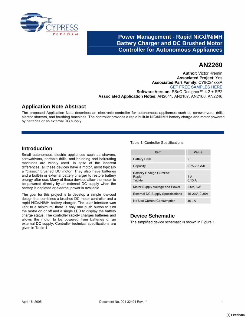
Device Schematic The simplified device schematic is shown in Figure 1.
[+] Feedback [+] Feedback
AN2260
Figure 1. Simplified Device Schematic
ADC
PSoC supply
Pulse-frequency modulator
DC supply
R1
R2
R3
Sw1Sw2
Sw3
R4
R5
Btn1
LED
Controller
Signal conditioning
R6
Switch-mode pump
R7
Rterm
Vdc1
L1 С1
VD1
Bat
MUX
M1
The device consists of:
Controller to implement battery charging and user-interface algorithms.
Spread spectrum pulse-frequency modulator.
Switch regulator, Sw1, L1, C1, VD1.
External DC supply inclusion-detection circuit, R1, R2.
Current sense resistor, R3.
Motor switch, M1 and Sw2, respectively.
Resistive divider, R4-R6, for motor or battery, Bat1, voltage measurement.
Battery switch, Sw3.
Switch mode pump (SMP) to increase battery voltage to acceptable levels for the PSoC® device.
Analog multiplexer MUX to commutate different analog signal sources.
Signal conditioning circuit for transforming input signals into valuable analog-to-digital conversion (ADC) levels.
Circuit for thermistor, Rterm, resistance measurement: Vdc, R7.
User interface elements of push button, Btn1, and LED.
The external DC supply voltage can be several times higher than nominal motor or battery voltage. This provides two significant advantages. It reduces the converter input current, which lowers the cost and weight of the external DC supply. It also allows the use of thinner connection wires and less expensive connectors. In this mode, the step-down converter switch duty cycle is small and the use of fixed-pulse width variable frequency control achieves a smaller duty cycle step.
The step-down switch regulator can be built around different configurations with different switch placement. The inverting regulator configuration is used in this project because of the following advantages:
Only one N-channel MOSFET is required, which can be controlled directly by the device without any translators.
The on-resistance for N-Channel transistor is less than for P-Channel in the same price range.
The inverting converter configuration is inherently protected from load overload due to limited energy quantity, which is transferred by inductor charge/discharge cycles.
April 15, 2005 Document No. 001-32404 Rev. ** 2
[+] Feedback [+] Feedback

AN2260
Figure 2. Complete Device Schematic
R1847k
C3
0.1u
R192.2M
LOAD1
LOAD2
R5300k
Q1IRLMS5703/SM
R1210k
Q3IRLML2402
VCPU
C4
10u
3.3V
LOAD
12345
J2
ISSP
BATON
XRES
XRES
PFM
D3
GREEN
TX232
R17470R
SMP
C22,2u
C110u
12
+
-
J1
DC Power
R16TERM
R910k
12
MG1MOTOR DC
R14470R
L26.8u
R1110k
VCPU
SW1
ON/OFF
R72.2k
BT1BAT
SMP
PFM
R13 0.1
MAINS
BATTERY
Q2BIRF7511
MOT
TERM
R15470R
R810k
R4300k
MOT
LED
13
D4BAT54WT1
P0[7]1
P0[5]2
P0[3]3
P0[1]4
P2[7]5
P2[5]6
P2[3]7
P2[1]8
SMP9
P1[7]10
P1[5]11
P1[3]12
P1[1]13
Vss14P1[0] 15P1[2] 16P1[4]
17P1[6] 18Xres 19
P2[0] 20P2[2] 21P2[4]22P2[6] 23
P0[0] 24P0[2] 25P0[4] 26P0[6] 27Vcc 28
U1
CY8C24423A_DIP28
BUTTON
D11n4007
Q2AIRF7511 or IRF 7513
R6110k
VD1MBR0520L
L16.8u
BATON
R1510k
2NiMH Cells
R2100k
C5
0.1u
MAINSR10 20R
LOAD1
D25.6V
LOAD2
The complete device schematic is shown in Figure 2. Because most of the analog signal processing is implemented inside the PSoC device, only a few external components are required. Q2A is the regulator switch. R1R2C3 is the external power-supply detection circuit. D2 suppresses possible high voltage spikes when the switch regulator has no load (both Q2B and Q1 are open.) Q2B is the motor control switch. Q1 and Q3 are battery switches. They can be single load switch (FDC6331L, FDR8521L) from Fairchild Semiconductor.
The SMP circuit consists of D4, L2, C4 and C5 elements. R19 completely discharges storage capacitors when the battery is disconnected. LED D3 is directly powered by a battery to offload the SMP when it is activated. The open drain low output drive mode at P1[4] is used. R18 provides logic 1 for port read-modify-write instructions when the LED is in off state. Button SW1 uses the internal pull-up resistor, so no external components are required. J2 is the ISSP/debug connector.
April 15, 2005 Document No. 001-32404 Rev. ** 3
[+] Feedback [+] Feedback
AN2260
Figure 3. PSoC Device Internals
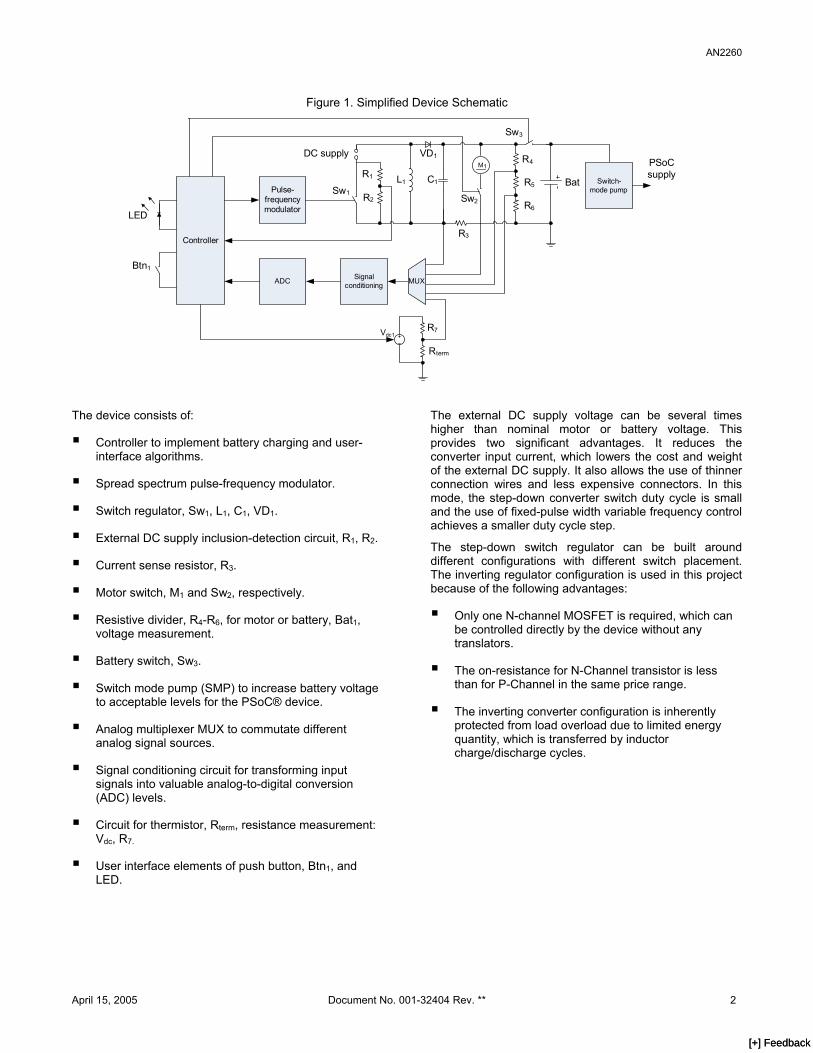
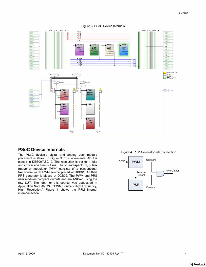
PSoC Device Internals The PSoC device’s digital and analog user module placement is shown in Figure 3. The incremental ADC is placed in DBB00/ASC10. The resolution is set to 11 bits and conversion time is 4 ms. The spread-spectrum, pulse-frequency modulator (PFM) consists of a conventional fixed-pulse width PWM source placed at DBB01. An 8-bit PRS generator is placed at DCB02. The PWM and PRS user modules compare outputs and are AND-ed using the row LUT. The idea for this source was suggested in Application Note AN2246 ”PWM Source - High Frequency, High Resolution.” Figure 4 shows the PFM internal interconnection.
Figure 4. PFM Generator Interconnection
PWM
PSR
PFM Output
Clock
TerminalCount
Compare
Compare
April 15, 2005 Document No. 001-32404 Rev. ** 4
[+] Feedback [+] Feedback
AN2260
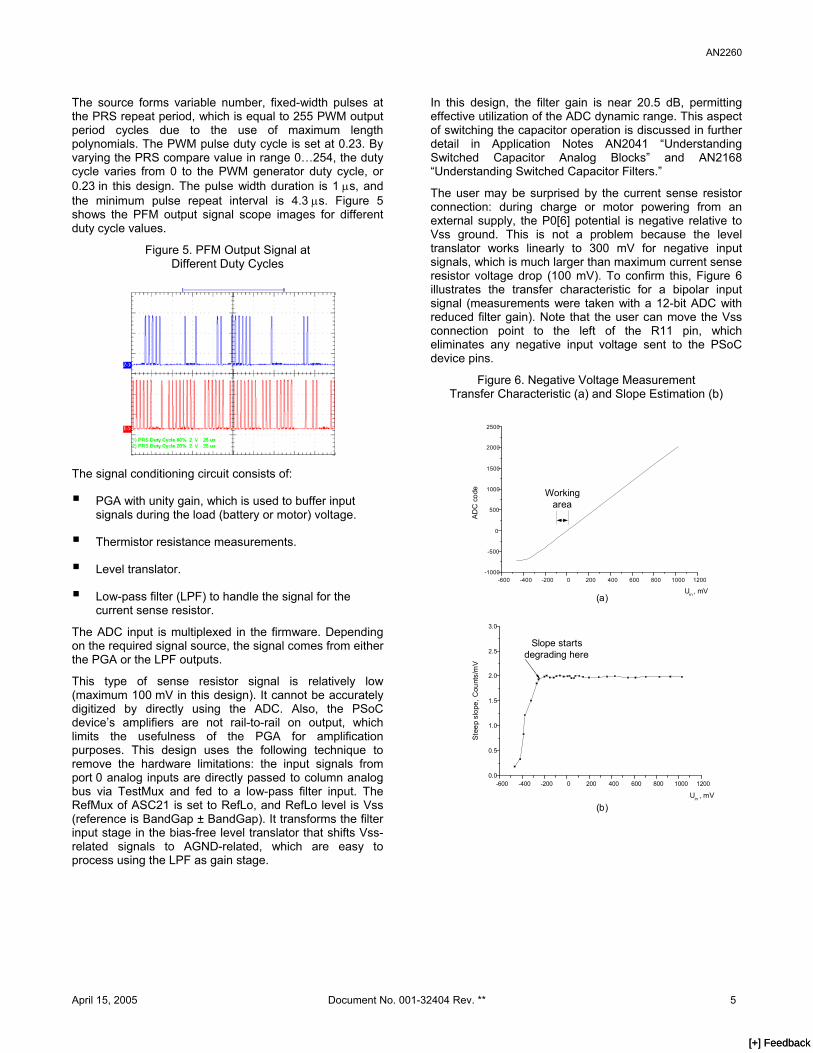
The source forms variable number, fixed-width pulses at the PRS repeat period, which is equal to 255 PWM output period cycles due to the use of maximum length polynomials. The PWM pulse duty cycle is set at 0.23. By varying the PRS compare value in range 0…254, the duty cycle varies from 0 to the PWM generator duty cycle, or 0.23 in this design. The pulse width duration is 1 μs, and the minimum pulse repeat interval is 4.3 μs. Figure 5 shows the PFM output signal scope images for different duty cycle values.
Figure 5. PFM Output Signal at Different Duty Cycles
The signal conditioning circuit consists of:
PGA with unity gain, which is used to buffer input signals during the load (battery or motor) voltage.
Thermistor resistance measurements.
Level translator.
Low-pass filter (LPF) to handle the signal for the current sense resistor.
The ADC input is multiplexed in the firmware. Depending on the required signal source, the signal comes from either the PGA or the LPF outputs.
This type of sense resistor signal is relatively low (maximum 100 mV in this design). It cannot be accurately digitized by directly using the ADC. Also, the PSoC device’s amplifiers are not rail-to-rail on output, which limits the usefulness of the PGA for amplification purposes. This design uses the following technique to remove the hardware limitations: the input signals from port 0 analog inputs are directly passed to column analog bus via TestMux and fed to a low-pass filter input. The RefMux of ASC21 is set to RefLo, and RefLo level is Vss (reference is BandGap ± BandGap). It transforms the filter input stage in the bias-free level translator that shifts Vss-related signals to AGND-related, which are easy to process using the LPF as gain stage.
In this design, the filter gain is near 20.5 dB, permitting effective utilization of the ADC dynamic range. This aspect of switching the capacitor operation is discussed in further detail in Application Notes AN2041 “Understanding Switched Capacitor Analog Blocks” and AN2168 “Understanding Switched Capacitor Filters.”
The user may be surprised by the current sense resistor connection: during charge or motor powering from an external supply, the P0[6] potential is negative relative to Vss ground. This is not a problem because the level translator works linearly to 300 mV for negative input signals, which is much larger than maximum current sense resistor voltage drop (100 mV). To confirm this, Figure 6 illustrates the transfer characteristic for a bipolar input signal (measurements were taken with a 12-bit ADC with reduced filter gain). Note that the user can move the Vss connection point to the left of the R11 pin, which eliminates any negative input voltage sent to the PSoC device pins.
Figure 6. Negative Voltage Measurement Transfer Characteristic (a) and Slope Estimation (b)
-600 -400 -200 0 200 400 600 800 1000 1200-1000
-500
0
500
1000
1500
2000
2500
AD
C c
ode
Uin , mV
-600 -400 -200 0 200 400 600 800 1000 12000.0
0.5
1.0
1.5
2.0
2.5
3.0
Ste
ep s
lope
, Cou
nts/
mV
Uin , mV
Slope starts degrading here
(a)
(b)
Working area
April 15, 2005 Document No. 001-32404 Rev. ** 5
[+] Feedback [+] Feedback

AN2260
April 15, 2005 Document No. 001-32404 Rev. ** 6
It is useful to observe the dynamic behavior of the internal variables (such as battery voltage and current, and state machine state) during controller firmware debugging. The serial transmitter, placed at DCB03, is used for this purpose. The dedicated PC software allows users to monitor details of the operation, which greatly simplifies firmware debugging. The communication speed is set to 19200 bps and the transmitter is clocked by a VC2 source.
Also, the Power Setting field under Global Resources needs to be set according to the selected supply voltage in order to correctly load oscillator and BandGap trim values. The CPU clock is 3 MHz, which allows the system to run from a 2.55V supply.
The Firmware The controller firmware consists of the following:
The slow mode main oscillator (6 MHz) in this design reduces power consumption at runtime. The SMP trip voltage determines the device’s supply level. It is set to 2.55V in sleep state when the device is not used and boosted to 4.64V when external power is available. This reduces switch regulator MOSFET resistive losses by providing a higher gate voltage. The user can set another power level (such as preset 3.25V supply when MOSFET with smaller threshold voltage is used).
Control state machine
Timekeeping services
Electrical values measurement routines
PFM duty cycle regulator
Battery charge algorithm
Sleep and Watchdog Timer handling
Runtime debug support
The control state machine provides device operation in different states, such as powering the motor from battery and external supply, battery charging support, low-supply sleep mode, and so on. Figure 7 shows the machine state diagram.
Figure 7. State Machine Diagram
Ext Motor
Bat Charge
Bat Power
b
Ext Power
Bat Motor
Sleep
a a
b
c
c
c
a d fe
Legend:a – button is pressed;b – external power source is connected;c – external power source is disconnected;d – no activity is detected for preset timeout;e – charge has been terminated;f – charge was not activated in this external power cycle or battery voltage is less than charge start voltage;g - button pressed or battery voltage dropped below preset threshold;h – sleep timer interrupt was triggered;
g
h
a
b
[+] Feedback [+] Feedback
AN2260
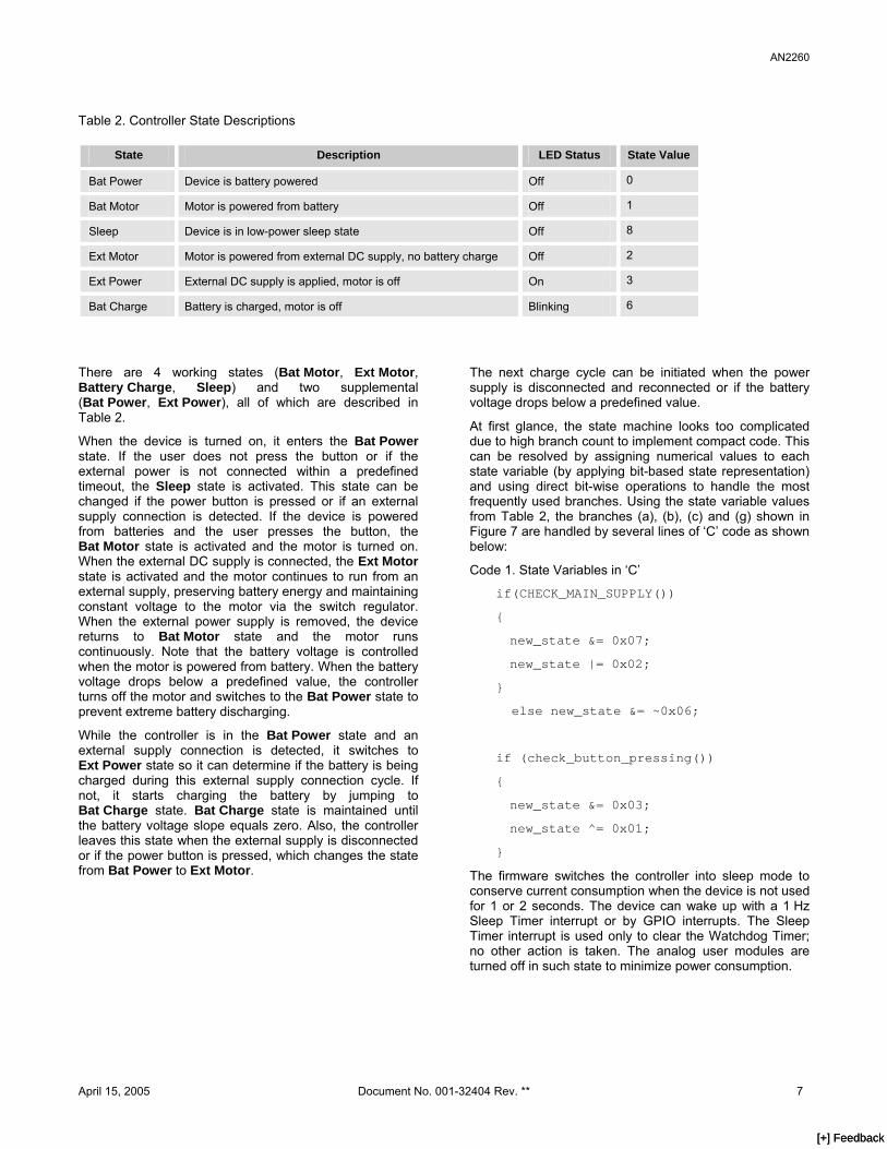
Table 2. Controller State Descriptions
State Description LED Status State Value
Bat Power Device is battery powered Off 0
Bat Motor Motor is powered from battery Off 1
Sleep Device is in low-power sleep state Off 8
Ext Motor Motor is powered from external DC supply, no battery charge Off 2
Ext Power External DC supply is applied, motor is off On 3
Bat Charge Battery is charged, motor is off Blinking 6
There are 4 working states (Bat Motor, Ext Motor, Battery Charge, Sleep) and two supplemental (Bat Power, Ext Power), all of which are described in Table 2.
When the device is turned on, it enters the Bat Power state. If the user does not press the button or if the external power is not connected within a predefined timeout, the Sleep state is activated. This state can be changed if the power button is pressed or if an external supply connection is detected. If the device is powered from batteries and the user presses the button, the Bat Motor state is activated and the motor is turned on. When the external DC supply is connected, the Ext Motor state is activated and the motor continues to run from an external supply, preserving battery energy and maintaining constant voltage to the motor via the switch regulator. When the external power supply is removed, the device returns to Bat Motor state and the motor runs continuously. Note that the battery voltage is controlled when the motor is powered from battery. When the battery voltage drops below a predefined value, the controller turns off the motor and switches to the Bat Power state to prevent extreme battery discharging.
While the controller is in the Bat Power state and an external supply connection is detected, it switches to Ext Power state so it can determine if the battery is being charged during this external supply connection cycle. If not, it starts charging the battery by jumping to Bat Charge state. Bat Charge state is maintained until the battery voltage slope equals zero. Also, the controller leaves this state when the external supply is disconnected or if the power button is pressed, which changes the state from Bat Power to Ext Motor.
The next charge cycle can be initiated when the power supply is disconnected and reconnected or if the battery voltage drops below a predefined value.
At first glance, the state machine looks too complicated due to high branch count to implement compact code. This can be resolved by assigning numerical values to each state variable (by applying bit-based state representation) and using direct bit-wise operations to handle the most frequently used branches. Using the state variable values from Table 2, the branches (a), (b), (c) and (g) shown in Figure 7 are handled by several lines of ‘C’ code as shown below:
Code 1. State Variables in ‘C’
if(CHECK_MAIN_SUPPLY())
{
new_state &= 0x07;
new_state |= 0x02;
}
else new_state &= ~0x06;
if (check_button_pressing())
{
new_state &= 0x03;
new_state ^= 0x01;
}
The firmware switches the controller into sleep mode to conserve current consumption when the device is not used for 1 or 2 seconds. The device can wake up with a 1 Hz Sleep Timer interrupt or by GPIO interrupts. The Sleep Timer interrupt is used only to clear the Watchdog Timer; no other action is taken. The analog user modules are turned off in such state to minimize power consumption.
April 15, 2005 Document No. 001-32404 Rev. ** 7
[+] Feedback [+] Feedback

AN2260
The GPIO interrupt occurs when the power button is pressed or an external power supply is connected. This event completely wakes up the controller by turning on the analog user modules.
Wakeup is handled by a state machine. It jumps to a new state depending upon the reason to wake up. After measuring the current and voltage, the PFM duty cycle control routines are executed in a loop. Figure 8 shows the controller operation in sleep and non-sleep states.
Figure 8. Controller Operation in Different States
Start
Initialize peripherials
Turn off analog part and prepare to sleep
Sleep
If sleep timer IRQ posted?
Turn on analog part and restore normal mode
Is state = Sleep?
Measure load current
Control PFM source
Measure load voltage
Run state machine
N
Y
Y
N
Service watchdog
Send debug information (optional)
As previously mentioned, the device uses dynamic power supply management to reduce current consumption. The power supply is set to a minimum value when in sleep mode and increases to higher a value when in normal mode.
The controller firmware (battery charging algorithms, electrical values measurement routines, PFM duty cycle regulator, etc.) includes timekeeping functions. There are state and interval timers with 1s resolution obtained by division VC3 interrupts at 600 Hz frequency. The precision of these timers is determined by the accuracy of the IMOs. The timers are primarily used by battery charging algorithms.
These timers can also be used to limit the duration of the motor-on states (Bat Motor, Ext Motor). This prevents overheating, as required in some applications such as power drills. The blinking LED, debounce push button switch, event generation, sleep periodic wakeup and debug information transmission are implemented using a low-accuracy Sleep Timer interrupt. The nominal interrupt rate is 1 or 8 Hz, depending on the present state.
The controller measures battery or motor voltage, charge/motor current and battery temperature. These values are used during rapid battery charge and to regulate the motor supply voltage when powered from an external DC supply. Voltage measurement is implemented by measuring the voltage drop on resistor R5 (see Figure 1) using a unity-gain PGA and an ADC. The value is measured for upper and lower R5 pins in sequence and the difference is calculated.
15 61
5 6 4
162
5 6 4
51 2
5 6 4
;
;
.
offlv fs fs
ref ref
offlv fs fs
ref ref
lv v v fs
ref
VR R VN N NR R R V V
VR VN N NR R R V V
R VN N N NR R R V
+= +
+ +
= ++ +
Δ = − =+ +
Equation 1
lV and refV are load and reference voltages
1offV is ADC/PGA offset voltage
fsN is full-scale ADC code range
vNΔ is ADC code difference, that is proportional to the measured voltage without the influence of offset voltage
Current measurement is implemented by measuring the voltage drop at R3 (Figure 1), using the modified LPF as a level translator and gain stage. The voltage levels for the right and left R3 pins are measured and the difference is calculated to eliminate the influence of the LPF/ADC/supply-pin offset on measurement accuracy.
3 21
22
32 1
;
;
.
LPF offc fs
ref
offc fs
ref
LPFc c c fs
ref
I R G VN N
VV
N NV
I R GN N N NV
− ⋅ ⋅ +=
=
⋅ ⋅Δ = − =
Equation 2
LPFG is LPF gain.
cNΔ is ADC code difference, which is proportional to the R3 current.
April 15, 2005 Document No. 001-32404 Rev. ** 8
[+] Feedback [+] Feedback

AN2260
2offV is cumulative offset voltage, which consists of
the following components:
ADC offset - 10 mV maximum.
LPF offset - 10 mV* LPFG , typically.
Vss pin supply offset, which is caused by voltage drop on internal die resistance and is proportional to PSoC device supply current via Vss pin. Typical values are less than 20 mV.
Temperature measurement is implemented by measuring the voltage drop on R7 (Figure 1) and applying, in sequence, two different voltages to the upper R7 pin and subtracting the results. The signal from the thermistor comes to the ADC via the PGA with unity gain. Bias voltages are formed using the continuous time TestMux to apply RefHi (2.6V) level at the first step and AGND (1.3V) at the next. This technique compensates for both the ADC/PGA offset and the possible offset caused by potential differences between the Vss internal die connection and the lower thermistor pin. (The sources of potential differences between the Vss internal die connection and the lower thermistor pin are the device’s internal die resistance, PCB voltage drop, battery pack voltage drop upon negative lead during charge, and so on.) Figure 9 and the following formulas illustrate how this works.
Figure 9. The Temperature Measurement
V1
V2
R7
Rterm
V0
+
Voff1
Ideal ADC
( )
( )
( )
1 0 1 1 07
2 0 1 27
2 1 2 17
;
;
.
fs termt off
ref term
fs termt off
ref term
fs termt
ref term
N RN V V V VV R R
N RN V V V VV R R
N RN N N V VV R R
⎡ ⎤= + + −⎢ ⎥+⎣ ⎦
⎡= + + −⎢ ⎥+⎣
Δ = − = −+
0⎤
⎦
Equation 3
1tN and 2tN are ADC codes for resistive divider bias voltages V1 and V2 (their difference is Vbandgap or 1.3V)
Voff1 and V0 are offset voltages (Voff1 is the same as in Equation (1))
tNΔ is ADC code difference
The thermistor transfer function is non-linear, but we do not need to obtain the temperature value in linear units for this design because the ratio of temperature increases is not used as rapid-charge termination criterion. Therefore, only the temperature thresholds during the charge need to be checked. This is done by analyzing the ADC code difference (
tNΔ ). A hysteresis is added for the bottom and upper bounds of the in/out temperature range to prevent multiple triggers when the temperature is close to the preset range (see Figure 10).
Figure 10. Temperature In-Range Checking
Irapid
Itricle
Icharge
TbatT1 T2 T3 T4
Hysteresis area
The device implements the rapid charge algorithm for NiCd/NiMH batteries. The batteries are charged by a constant current in rapid charge mode with 1 C rate (the C rate is the hour capacity of the battery at 600 mA) when the battery temperature is in the allowed range. When the battery is too hot or cold, the controller reduces the charge current using trickle charge mode. Note that the battery temperature is measured once per 4s using an interval timer timeout.
The charge is normally terminated when the battery voltage stops increasing; this termination criterion is suitable for either NiCd or NiMH batteries. The integration criterion is used for battery voltage slope analysis to get the best noise immunity. During the first step, the measured battery voltage is filtered using a simple IIR LPF filter.
( ) 11j jy yγ − jv= − + Equation 4
jy is filter output signal j sample
jv is input voltage sample
, 1γ γ < is filter coefficient
This filter is characterized by the gain 1γ − . Implementation minimizes the influence of fixed-point rounding errors and improves the accuracy of small voltage variation detection. Instead of dividing/multiplying the binary shift,
2 Kγ −= was used, where K=2. Each voltage measurement result passes through this filter.
April 15, 2005 Document No. 001-32404 Rev. ** 9
[+] Feedback [+] Feedback
AN2260
April 15, 2005 Document No. 001-32404 Rev. ** 10
The device employs the PFM duty cycle regulator to maintain the charge current or motor voltage, depending on the controller state (Bat Charge or Ext Motor). The regulator is an adaptive step integrator. Figure 13 shows PFM duty cycle regulator dataflow.
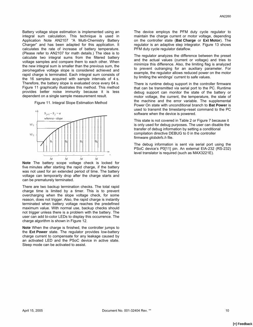
Battery voltage slope estimation is implemented using an integral sum calculation. This technique is used in Application Note AN2107 “A Multi-Chemistry Battery Charger” and has been adapted for this application. It calculates the rate of increase of battery temperature. (Please refer to AN2107 for math details.) The idea is to calculate two integral sums from the filtered battery voltage samples and compare them to each other. When the new integral sum is smaller than the previous sum, the zero/negative voltage slope is considered achieved and rapid charge is terminated. Each integral sum consists of the 16 samples acquired with sample intervals of 4 s. Therefore, the battery slope is evaluated once every 64 s. Figure 11 graphically illustrates this method. This method provides better noise immunity because it is less dependent on a single sample measurement result.
The regulator analyzes the difference between the preset and the actual values (current or voltage) and tries to minimize this difference. Also, the limiting flag is analyzed to prevent outranging for an auxiliary parameter. For example, the regulator allows reduced power on the motor by limiting the windings’ current to safe values.
There is runtime debug support in the controller firmware that can be transmitted via serial port to the PC. Runtime debug support can monitor the state of the battery or motor voltage, the current, the temperature, the state of the machine and the error variable. The supplemental Power On state with unconditional branch to Bat Power is used to transmit the timestamp-reset command to the PC software when the device is powered.
Figure 11. Integral Slope Estimation Method
t
U
S1 S2 S3 S4
2UΔ
2UΔ
tΔtΔtΔtΔ
slopeawhere
aSS jj
−
−+ ~1
This state is not covered in Table 2 or Figure 7 because it is only used for debug purposes. The user can disable the transfer of debug information by setting a conditional compilation directive DEBUG to 0 in the controller firmware globdefs.h file.
The debug information is sent via serial port using the PSoC device’s P0[11] pin. An external EIA-232 (RS-232) level translator is required (such as MAX3221E).
Note The battery scope voltage check is locked for five minutes after starting the rapid charge, if the battery was not used for an extended period of time. The battery voltage can temporarily drop after the charge starts and can be prematurely terminated.
There are two backup termination checks. The total rapid charge time is limited by a timer. This is to prevent overcharging when the slope voltage check, for some reason, does not trigger. Also, the rapid charge is instantly terminated when battery voltage reaches the predefined maximum value. With normal use, backup checks should not trigger unless there is a problem with the battery. The user can add bi-color LEDs to display this occurrence. The charge algorithm is shown in Figure 12.
Note When the charge is finished, the controller jumps to the Ext Power state. The regulator provides low-battery charge current to compensate for any leakage caused by an activated LED and the PSoC device in active state. Sleep mode can be activated to assist.
[+] Feedback [+] Feedback

AN2260
Figure 12. Battery Charge Algorithm
Start
Initialize variables and timers, set trickle charge
Is 4s timeout expired?
Reinitialize 4s timer, measure battery
temperature
Is temperature OK?
Set rapid charge, resume total charge timer
Set trickle charge, reset charge termination check, suspend total charge timer
Is charge longer than 300s?
Is zero voltage slope detected?
Stop, charge completed well
Measure battery voltage and charge current
Is Vbat > Vbat_max
Is tcharge > ttotal
Stop, overvoltage error
Stop, timeout error
Regulate charge current
YN
Y
N
Y
N
Y
Y
N
N
Figure 13. Duty Cycle Regulator
−Step
estimator(lookup)
Limiting control + Range
checkingActual
Preset Limiting
Duty cycle
April 15, 2005 Document No. 001-32404 Rev. ** 11
[+] Feedback [+] Feedback

AN2260
The PC software that monitors the system is a multithread Windows application. It is simplified in Application Note AN2107 A Multi-Chemistry Battery Charger and allows users to view graphs displaying battery or motor supply voltage, charge/motor current, and temperature.
State and error conditions can also be viewed. The software allows users to store and compare collected data for further analysis. Figure 14 shows examples of the graphs. The software was written using Borland® Delphi™7.
Figure 14. Example of Software Interface
Note Battery was Slightly Discharged Before Charging Began
Summary This Application Note describes a simple, low-cost battery charger with a DC motor controller. The hardware and firmware can be easily adapted to meet end application demands. The following modifications can be implemented:
Charge algorithm can be adapted to support LiIon batteries.
Current sense resistor can be eliminated. Battery charge current can be found mathematically by measuring the switch regulator input, the output voltages and using the switch regulator look-up table. NiCd/NiMH batteries are not very sensitive to the absolute value of the charge current, and 10-15 percent can be tolerated without problems.
Figure 15. Device Photograph
April 15, 2005 Document No. 001-32404 Rev. ** 12
[+] Feedback [+] Feedback
AN2260
About the Author Name: Victor Kremin
Title: Associate Professor Background: Victor earned radiophysics diploma
in 1996 from Ivan Franko National Lviv University, PhD degree in Computer Aided Design Systems in 2000, and is presently working as Associate Professor at National University "Lvivska Polytechnika" (Lviv, Ukraine). His interests involve the full cycle of embedded system design including various processors, operation systems, and target applications.
Contact: [email protected]
In March of 2007, Cypress recataloged all of its Application Notes using a new documentation number and revision code. This new documentation number and revision code (001-xxxxx, beginning with rev. **), located in the footer of the document, will be used in all subsequent revisions.
PSoC is a registered trademark of Cypress Semiconductor Corp. "Programmable System-on-Chip," PSoC Designer, and PSoC Express are trademarks of Cypress Semiconductor Corp. All other trademarks or registered trademarks referenced herein are the property of their respective owners.
Cypress Semiconductor 198 Champion Court
San Jose, CA 95134-1709 Phone: 408-943-2600
Fax: 408-943-4730 http://www.cypress.com/
© Cypress Semiconductor Corporation, 2005-2007. The information contained herein is subject to change without notice. Cypress Semiconductor Corporation assumes no responsibility for the use of any circuitry other than circuitry embodied in a Cypress product. Nor does it convey or imply any license under patent or other rights. Cypress products are not warranted nor intended to be used for medical, life support, life saving, critical control or safety applications, unless pursuant to an express written agreement with Cypress. Furthermore, Cypress does not authorize its products for use as critical components in life-support systems where a malfunction or failure may reasonably be expected to result in significant injury to the user. The inclusion of Cypress products in life-support systems application implies that the manufacturer assumes all risk of such use and in doing so indemnifies Cypress against all charges.
This Source Code (software and/or firmware) is owned by Cypress Semiconductor Corporation (Cypress) and is protected by and subject to worldwide patent protection (United States and foreign), United States copyright laws and international treaty provisions. Cypress hereby grants to licensee a personal, non-exclusive, non-transferable license to copy, use, modify, create derivative works of, and compile the Cypress Source Code and derivative works for the sole purpose of creating custom software and or firmware in support of licensee product to be used only in conjunction with a Cypress integrated circuit as specified in the applicable agreement. Any reproduction, modification, translation, compilation, or representation of this Source Code except as specified above is prohibited without the express written permission of Cypress.
Disclaimer: CYPRESS MAKES NO WARRANTY OF ANY KIND, EXPRESS OR IMPLIED, WITH REGARD TO THIS MATERIAL, INCLUDING, BUT NOT LIMITED TO, THE IMPLIED WARRANTIES OF MERCHANTABILITY AND FITNESS FOR A PARTICULAR PURPOSE. Cypress reserves the right to make changes without further notice to the materials described herein. Cypress does not assume any liability arising out of the application or use of any product or circuit described herein. Cypress does not authorize its products for use as critical components in life-support systems where a malfunction or failure may reasonably be expected to result in significant injury to the user. The inclusion of Cypress’ product in a life-support systems application implies that the manufacturer assumes all risk of such use and in doing so indemnifies Cypress against all charges.
Use may be limited by and subject to the applicable Cypress software license agreement.
April 15, 2005 Document No. 001-32404 Rev. ** 13
[+] Feedback [+] Feedback