power management switch ics for pcs and digital … semiconductor... · 2012-10-15 · power...
TRANSCRIPT
BD2062FJ
1/16
www.rohm.com 2011.05 - Rev.B© 2011 ROHM Co., Ltd. All rights reserved.
Power Management Switch ICs for PCs and Digital Consumer Products 2ch High Side Switch ICs for USB Devices and Memory Cards BD2062FJ,BD2066FJ
Description
High side switch for USB is a high side switch having over-current protection used in power supply line of universal serial bus (USB). Its switch unit has two channels of N-channel power MOSFET. And, over-current detection circuit, thermal shutdown circuit, under-voltage lockout and soft-start circuit are built in.
Features
1) Dual N-MOS High Side Switch 2) Current Limit Threshold 2.4A 3) Control Input Logic Active-Low : BD2062FJ Active-High : BD2066FJ 4) Soft-Start Circuit 5) Over-Current Detection 6) Thermal Shutdown 7) Under-Voltage Lockout 8) Open-Drain Error Flag Output 9) Reverse Current Protection When Switch Off 10) Flag Output Delay Filter Built In 11) Power Supply Voltage Range 2.7V~5.5V 12) TTL Enable Input 13) 0.8ms Typical Rise Time 14) 1 A Max Standby Current
Applications
PC, PC peripheral USB hub in consumer appliances, Car accessory, and so forth
Line Up Matrix
Parameter BD2062FJ BD2066FJ
Current limit threshold (A) 2.4 2.4
Control input logic Low High
Number of channels 2ch 2ch
Package SOP-J8 SOP-J8
No.11029EBT15
Technical Note
2/16
BD2062FJ,BD2066FJ
www.rohm.com 2011.05 - Rev.B© 2011 ROHM Co., Ltd. All rights reserved.
Absolute Maximum Ratings (Ta=25 )
Parameter Symbol Ratings Unit
Supply voltage VIN -0.3 ~ 6.0 V
Enable input voltage VEN -0.3 ~ 6.0 V
/OC voltage V/OC -0.3 ~ 6.0 V
/OC sink current IS/OC ~ 5 mA
OUT voltage VOUT -0.3 ~ 6.0 V
Storage temperature TSTG -55 ~ 150
Power dissipation Pd 675*1
mW
*1 Mounted on 70mm * 70mm * 1.6mm glass-epoxy PCB. Derating : 5.4mW/ oC above Ta=25
oC
* This product is not designed for protection against radioactive rays.
Operating Conditions
Parameter SymbolRatings
Unit Min. Typ. Max.
Operating voltage VIN 2.7 - 5.5 V
Operating temperature TOPR -40 - 85
Technical Note
3/16
BD2062FJ,BD2066FJ
www.rohm.com 2011.05 - Rev.B© 2011 ROHM Co., Ltd. All rights reserved.
Electrical Characteristics
BD2062FJ (Unless otherwise specified VIN = 5.0V, Ta = 25 )
Parameter Symbol Limits
Unit Conditions Min. Typ. Max.
Operating current IDD - 130 180 A V/EN = 0V , OUT=OPEN
Standby current ISTB - 0.01 1 A V/EN = 5V , OUT=OPEN
/EN input voltage V/EN 2.0 - - V High input
V/EN - - 0.8 V Low input
/EN input current I/EN -1.0 0.01 1.0 A V/EN = 0V or V/EN = 5V
/OC output low voltage V/OCL - - 0.5 V I/OC = 1mA
/OC output leak current IL/OC - 0.01 1 A V/OC = 5V
/OC delay time T/OC 10 15 20 ms
On-resistance RON - 80 125 m IOUT = 500mA
Switch leak current ILSW - - 1.0 A V/EN = 5V, VOUT = 0V
Reverse leak current ILREV - - 1.0 A VOUT = 5.5V, VIN = 0V
Current limit threshold ITH 1.5 2.4 3.0 A
Short circuit current ISC 1.1 1.5 2.1 A VOUT = 0V
CL = 47 F (RMS)
Output rise time TON1 - 0.8 10 ms RL = 10
Output turn-on time TON2 - 1.1 20 ms RL = 10
Output fall time TOFF1 - 5 20 s RL = 10
Output turn-off time TOFF2 - 10 40 s RL = 10
UVLO threshold VTUVH 2.1 2.3 2.5 V Increasing VIN
VTUVL 2.0 2.2 2.4 V Decreasing VIN
Technical Note
4/16
BD2062FJ,BD2066FJ
www.rohm.com 2011.05 - Rev.B© 2011 ROHM Co., Ltd. All rights reserved.
BD2066FJ (Unless otherwise specified VIN = 5.0V, Ta = 25 )
Parameter Symbol Limits
Unit Condition Min. Typ. Max.
Operating current IDD - 130 180 A VEN = 5V , OUT=OPEN
Standby current ISTB - 0.01 1 A VEN = 0V , OUT=OPEN
EN input voltage VEN 2.0 - - V High input
VEN - - 0.8 V Low input
EN input current IEN -1.0 0.01 1.0 A VEN = 0V or VEN = 5V
/OC output low voltage V/OCL - - 0.5 V I/OC = 1mA
/OC output leak current IL/OC - 0.01 1 A V/OC = 5V
/OC delay time T/OC 10 15 20 ms
On-resistance RON - 80 125 m IOUT = 500mA
Switch leak current ILSW - - 1.0 A VEN = 0V, VOUT = 0V
Reverse leak current ILREV - - 1.0 A VOUT = 5.5V, VIN = 0V
Current limit threshold ITH 1.5 2.4 3.0 A
Short circuit current ISC 1.1 1.5 2.1 A VOUT = 0V CL = 47 F (RMS)
Output rise time TON1 - 0.8 10 ms RL = 10
Output turn-on time TON2 - 1.1 20 ms RL = 10
Output fall time TOFF1 - 5 20 s RL = 10
Output turn-off time TOFF2 - 10 40 s RL = 10
UVLO threshold VTUVH 2.1 2.3 2.5 V Increasing VIN
VTUVL 2.0 2.2 2.4 V Decreasing VIN
Technical Note
5/16
BD2062FJ,BD2066FJ
www.rohm.com 2011.05 - Rev.B© 2011 ROHM Co., Ltd. All rights reserved.
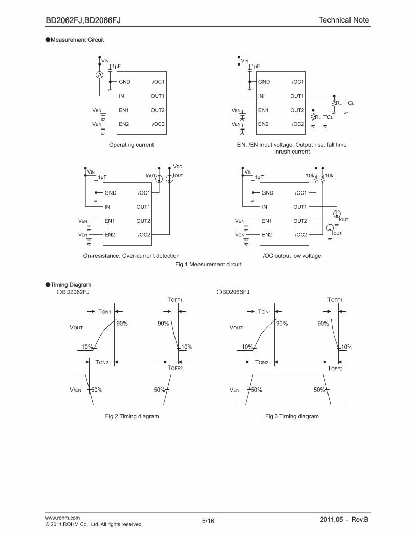
Measurement Circuit
GND
IN
EN1
EN2
/OC1
OUT1
OUT2
/OC2
VIN
VEN
1µF
VEN
GND
IN
EN1
EN2
/OC1
OUT1
OUT2
/OC2
VIN
VEN
1µF
VEN
RL CL
RL CL
Operating current EN, /EN input voltage, Output rise, fall time Inrush current
GND
IN
EN1
EN2
/OC1
OUT1
OUT2
/OC2
VIN
VEN
1µF
VEN
IOUTIOUT
VDD
GND
IN
EN1
EN2
/OC1
OUT1
OUT2
/OC2
VIN
VEN
1µF
VEN IOUT
10k10k
IOUT
On-resistance, Over-current detection /OC output low voltage
Fig.1 Measurement circuit
Timing Diagram
BD2062FJ BD2066FJ
TON2
50%
TON1
10%
90%
50%
90%
10%
TOFF1
VOUT
V/EN
TOFF2
TON2
50%
TON1
10%
90%
50%
90%
10%
TOFF1
VOUT
VEN
TOFF2
Fig.2 Timing diagram Fig.3 Timing diagram
Technical Note
6/16
BD2062FJ,BD2066FJ
www.rohm.com 2011.05 - Rev.B© 2011 ROHM Co., Ltd. All rights reserved.
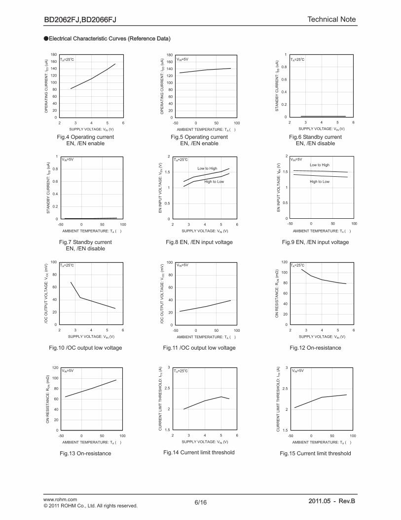
Electrical Characteristic Curves (Reference Data)
1.5
2
2.5
3
-50 0 50 100
AMBIENT TEMPERATURE: TA ( )
CU
RR
EN
T L
IMIT
TH
RE
SH
OL
D:
I TH (
A)
1.5
2
2.5
3
2 3 4 5 6
SUPPLY VOLTAGE: VIN (V)
CU
RR
EN
T L
IMT
TH
RE
SH
OL
D:
I TH (
A)
0
20
40
60
80
100
120
-50 0 50 100
AMBIENT TEMPERATURE: TA ( )
ON
RE
SIS
TA
NC
E:
RO
N (
m)
0
20
40
60
80
100
120
2 3 4 5 6
SUPPLY VOLTAGE: VIN (V)
ON
RE
SIS
TA
NC
E:
RO
N (
m)
0
20
40
60
80
100
-50 0 50 100
AMBIENT TEMPERATURE: TA ( )
/OC
OU
TP
UT
VO
LT
AG
E:
V/O
C (
mV
)
0
20
40
60
80
100
2 3 4 5 6
SUPPLY VOLTAGE: VIN (V)
/OC
OU
TP
UT
VO
LT
AG
E:
V/O
C (
mV
)
0
0.5
1
1.5
2
-50 0 50 100
AMBIENT TEMPERATURE: TA ( )
EN
IN
PU
T V
OL
TA
GE
: V E
N (
V)
0
0.5
1
1.5
2
2 3 4 5 6
SUPPLY VOLTAGE: VIN (V)
EN
IN
PU
T V
OL
TA
GE
: V
EN (
V)
0
0.2
0.4
0.6
0.8
1
-50 0 50 100
AMBIENT TEMPERATURE: TA ( )
ST
AN
DB
Y C
UR
RE
NT
: I D
D (
uA
)
0
0.2
0.4
0.6
0.8
1
2 3 4 5 6
SUPPLY VOLTAGE: VIN (V)
ST
AN
DB
Y C
UR
RE
NT
: I D
D (
uA
)
0
20
40
60
80
100
120
140
160
180
-50 0 50 100
AMBIENT TEMPERATURE: TA ( )
OP
ER
AT
ING
CU
RR
EN
T:
I DD (
uA
)
0
20
40
60
80
100
120
140
160
180
2 3 4 5 6
SUPPLY VOLTAGE: VIN (V)
OP
ER
AT
ING
CU
RR
EN
T:
I DD (
uA
)
Fig.14 Current limit threshold
Fig.4 Operating current EN, /EN enable
Fig.5 Operating current EN, /EN enable
Fig.6 Standby current EN, /EN disable
Fig.7 Standby current EN, /EN disable
Fig.8 EN, /EN input voltage Fig.9 EN, /EN input voltage
Fig.10 /OC output low voltage Fig.11 /OC output low voltage Fig.12 On-resistance
Fig.13 On-resistance
TA=25 TA=25 VIN=5V
VIN=5V TA=25
TA=25 TA=25
TA=25
VIN=5V
VIN=5V
VIN=5V VIN=5V
Low to High
High to Low High to Low
Low to High
Fig.15 Current limit threshold

Technical Note
7/16
BD2062FJ,BD2066FJ
www.rohm.com 2011.05 - Rev.B© 2011 ROHM Co., Ltd. All rights reserved.
0
5
10
15
20
-50 0 50 100
AMBIENT TEMPERATURE: TA ( )
/OC
DE
LA
Y T
IME
: T /
OC (
ms)
0
5
10
15
20
2 3 4 5 6
SUPPLY VOLTAGE: VIN (V)
/OC
DE
LA
Y T
IME
: T /
OC (
ms)
0
2
4
6
8
10
-50 0 50 100
0
2
4
6
8
10
2 3 4 5 6
SUPPLY VOLTAGE: VIN (V)
TU
RN
OF
F T
IME
: T
OF
F2 (
us)
0
1
2
3
4
5
-50 0 50 100
AMBIENT TEMPERATURE: TA ( )
FA
LL
TIM
E:
TO
FF
1 (
us)
0
1
2
3
4
5
2 3 4 5 6
SUPPLY VOLTAGE: VIN (V)
FA
LL
TIM
E:
TO
FF
1 (
us)
0
0.2
0.4
0.6
0.8
1
-50 0 50 100
AMBIENT TEMPERATURE: TA ( )
TU
RN
ON
TIM
E:
TO
N2 (
ms)
0
0.2
0.4
0.6
0.8
1
2 3 4 5 6
SUPPLY VOLTAGE: VIN (V)
TU
RN
ON
TIM
E:
TO
N2 (
ms)
0
0.2
0.4
0.6
0.8
1
-50 0 50 100
AMBIENT TEMPERATURE: TA( )
RIS
E T
IME
: T O
N1(
ms)
0
0.2
0.4
0.6
0.8
1
2 3 4 5 6
SUPPLY VOLTAGE: VIN (V)
RIS
E T
IME
: T O
N1
(ms)
0
0.5
1
1.5
2
-50 0 50 100
AMBIENT TEMPERATURE: TA ( )
SH
OR
T C
IRC
UIT
CU
RR
EN
T:I S
C (
A)
0
0.2
0.4
0.6
0.8
1
2 3 4 5 6
SUPPLY VOLTAGE: VIN (V)
OU
TP
UT
RIS
E T
IME
: T O
N1 (m
s)
Fig.16 Short circuit current Fig.17 Short circuit current Fig.18 Output rise time
Fig.19 Output rise time Fig.20 Output turn-on time Fig.21 Output turn-on time
Fig.22 Output fall time Fig.23 Output fall time Fig.24 Output turn-off time
Fig.25 Output turn-off time Fig.26 /OC delay time Fig.27 /OC delay time
VIN=5V
TA=25 VIN=5V
TA=25 TA=25
VIN=5V
TA=25 VIN=5V TA=25
VIN=5V TA=25 VIN=5V
Technical Note
8/16
BD2062FJ,BD2066FJ
www.rohm.com 2011.05 - Rev.B© 2011 ROHM Co., Ltd. All rights reserved.
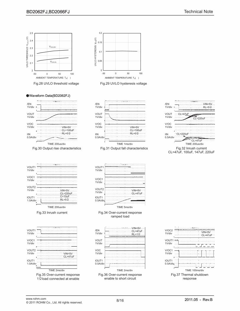
Waveform Data(BD2062FJ)
0
0.05
0.1
0.15
0.2
-50 0 50 100
AMBIENT TEMPERATURE: TA( )
UV
LO
HY
ST
ER
ES
IS:
V HY
S(V
)
2
2.1
2.2
2.3
2.4
2.5
-50 0 50 100
AMBIENT TEMPERATURE: TA( )
UV
LO
TH
RE
SH
OL
D:
VU
VLO (
V)
Fig.28 UVLO threshold voltage Fig.29 UVLO hysteresis voltage
Fig.30 Output rise characteristics Fig.31 Output fall characteristics Fig.32 Inrush current CL=47uF, 100uF, 147uF, 220uF
Fig.33 Inrush current Fig.34 Over-current responseramped load
Fig.35 Over-current response
1 load connected at enable
Fig.36 Over-current responseenable to short circuit
Fig.37 Thermal shutdown response
VIN=5V CL=100uF
RL=5
/EN 1V/div
VOUT 1V/div
V/OC 1V/div
IIN 0.5A/div
TIME 200us/div
/EN 1V/div
VOUT 1V/div
V/OC 1V/div
IIN 0.5A/div
/EN 1V/div
VOUT 1V/div
V/OC 1V/div
IIN 0.5A/div
VOUT1 1V/div
VOUT2 1V/div
V/OC1 1V/div
IOUT1 1.0A/div
VOUT2 1V/div
VOUT11V/div
V/OC1 1V/div
IOUT1 0.5A/div
VOUT1 1V/div
V/OC1 1V/div
VOUT2 1V/div
IOUT1 1.0A/div
/EN 1V/div
VOUT 1V/div
VOC 1V/div
IOUT1 0.5A/div
V/OC2 1V/div
VOUT1 1V/div
V/OC1 1V/div
IOUT1 0.5A/div
TIME 1ms/div TIME 200us/div
TIME 200us/div TIME 5ms/div
TIME 2ms/div TIME 2ms/div TIME 100ms/div
VIN=5V CL=100uF
RL=5
VIN=5V
RL=5
CL=47uF
CL=220uF
CL=47uF
CL=220uF
VIN=5V CL=220uF C=10uF
RL=5
VIN=5V CL=47uF
VIN=5V CL=47uF
VIN=5V CL=47uF
RL=1
VIN=5V CL=47uF
VUVLOH
VUVLOL
Technical Note
9/16
BD2062FJ,BD2066FJ
www.rohm.com 2011.05 - Rev.B© 2011 ROHM Co., Ltd. All rights reserved.
Block Diagram
Gate
Logic1
OCD1Charge
Pump1
TSD1
UVLO
Charge
Pump2 OCD2
Gate
Logic2
TSD2
/EN1
EN1
IN
/EN2
EN2
GND
/OC1
OUT1
OUT2
/OC2
Delay
Delay
1
2
8
7
GND
IN
/OC1
OUT1
3/EN1
(EN1)
4
6
5
OUT2
/OC2
Top View
/EN2
(EN2)
Fig.38 Block diagram Fig.39 Pin configuration
Pin Description
BD2062FJ
Pin No. Symbol I / O Pin function
1 GND - Ground.
2 IN - Power supply input. Input terminal to the switch and power supply input terminal of the internal circuit.
3, 4 /EN I Enable input. Switch on at Low level. High level input > 2.0V, Low level input < 0.8V.
5, 8 /OC O Error flag output. Low at over-current, thermal shutdown. Open drain output.
6, 7 OUT O Switch output.
BD2066FJ
Pin No. Symbol I / O Pin function
1 GND - Ground.
2 IN - Power supply input. Input terminal to the switch and power supply input terminal of the internal circuit.
3, 4 EN I Enable input. Switch on at High level. High level input > 2.0V, Low level input < 0.8V
5, 8 /OC O Error flag output. Low at over-current, thermal shutdown. Open drain output.
6, 7 OUT O Switch output.
Technical Note
10/16
BD2062FJ,BD2066FJ
www.rohm.com 2011.05 - Rev.B© 2011 ROHM Co., Ltd. All rights reserved.
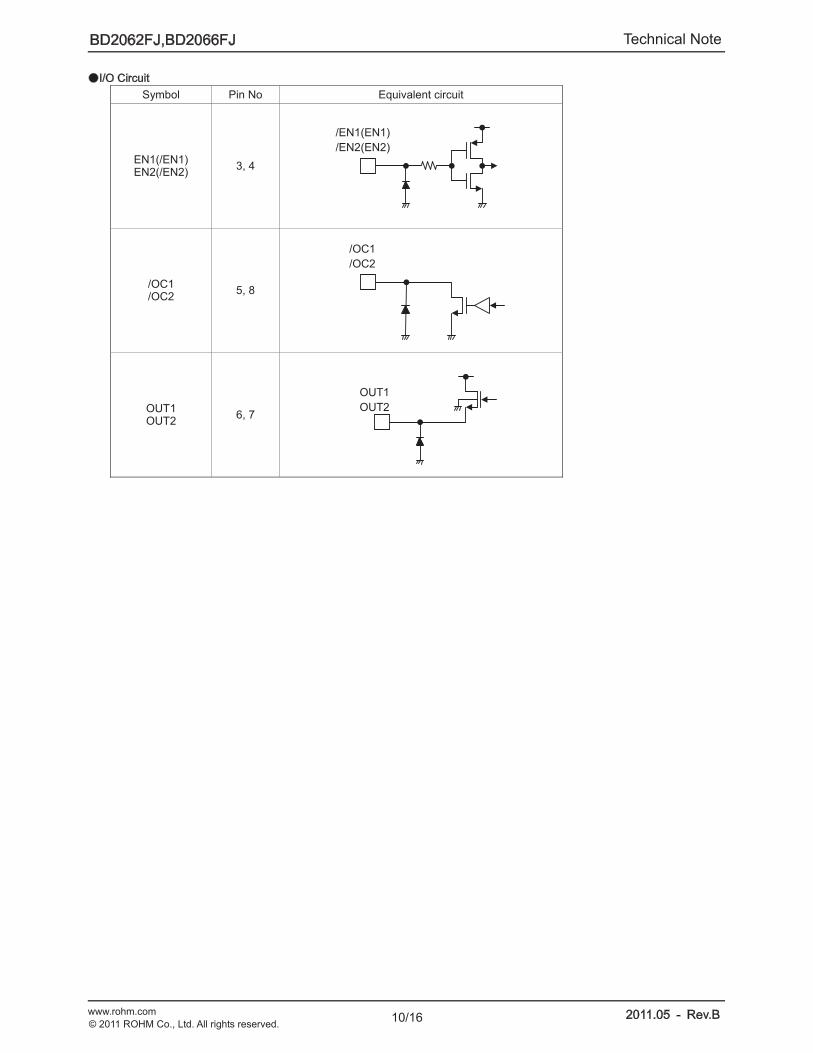
I/O Circuit
Symbol Pin No Equivalent circuit
EN1(/EN1) EN2(/EN2)
3, 4
/EN1(EN1)
/EN2(EN2)
/OC1 /OC2
5, 8
/OC1
/OC2
OUT1 OUT2
6, 7
OUT1
OUT2
Technical Note
11/16
BD2062FJ,BD2066FJ
www.rohm.com 2011.05 - Rev.B© 2011 ROHM Co., Ltd. All rights reserved.
Functional Description
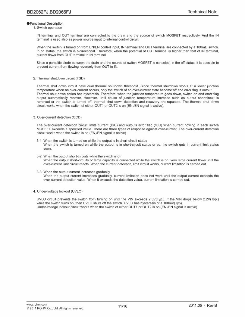
1. Switch operation IN terminal and OUT terminal are connected to the drain and the source of switch MOSFET respectively. And the IN terminal is used also as power source input to internal control circuit. When the switch is turned on from EN/EN control input, IN terminal and OUT terminal are connected by a 100m switch. In on status, the switch is bidirectional. Therefore, when the potential of OUT terminal is higher than that of IN terminal, current flows from OUT terminal to IN terminal. Since a parasitic diode between the drain and the source of switch MOSFET is canceled, in the off status, it is possible to prevent current from flowing reversely from OUT to IN.
2. Thermal shutdown circuit (TSD) Thermal shut down circuit have dual thermal shutdown threshold. Since thermal shutdown works at a lower junction temperature when an over-current occurs, only the switch of an over-current state become off and error flag is output. Thermal shut down action has hysteresis. Therefore, when the junction temperature goes down, switch on and error flag output automatically recover. However, until cause of junction temperature increase such as output shortcircuit is removed or the switch is turned off, thermal shut down detection and recovery are repeated. The thermal shut down circuit works when the switch of either OUT1 or OUT2 is on (EN,/EN signal is active).
3. Over-current detection (OCD) The over-current detection circuit limits current (ISC) and outputs error flag (/OC) when current flowing in each switch MOSFET exceeds a specified value. There are three types of response against over-current. The over-current detection circuit works when the switch is on (EN,/EN signal is active). 3-1. When the switch is turned on while the output is in short-circuit status
When the switch is turned on while the output is in short-circuit status or so, the switch gets in current limit status soon.
3-2. When the output short-circuits while the switch is on
When the output short-circuits or large capacity is connected while the switch is on, very large current flows until the over-current limit circuit reacts. When the current detection, limit circuit works, current limitation is carried out.
3-3. When the output current increases gradually
When the output current increases gradually, current limitation does not work until the output current exceeds the over-current detection value. When it exceeds the detection value, current limitation is carried out.
4. Under-voltage lockout (UVLO) UVLO circuit prevents the switch from turning on until the VIN exceeds 2.3V(Typ.). If the VIN drops below 2.2V(Typ.) while the switch turns on, then UVLO shuts off the switch. UVLO has hysteresis of a 100mV(Typ). Under-voltage lockout circuit works when the switch of either OUT1 or OUT2 is on (EN,/EN signal is active).
Technical Note
12/16
BD2062FJ,BD2066FJ
www.rohm.com 2011.05 - Rev.B© 2011 ROHM Co., Ltd. All rights reserved.
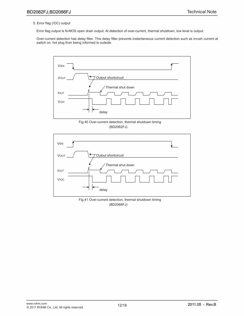
5. Error flag (/OC) output Error flag output is N-MOS open drain output. At detection of over-current, thermal shutdown, low level is output. Over-current detection has delay filter. This delay filter prevents instantaneous current detection such as inrush current at switch on, hot plug from being informed to outside.
V/EN
VOUT
IOUT
V/OC
Output shortcircuit
Thermal shut down
delay
Fig.40 Over-current detection, thermal shutdown timing
(BD2062FJ)
VEN
VOUT
IOUT
V/OC
Output shortcircuit
Thermal shut down
delay
Fig.41 Over-current detection, thermal shutdown timing
(BD2066FJ)
Technical Note
13/16
BD2062FJ,BD2066FJ
www.rohm.com 2011.05 - Rev.B© 2011 ROHM Co., Ltd. All rights reserved.
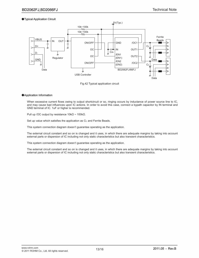
Typical Application Circuit
ON/OFF
OC
OC
ON/OFF
GND
IN
/EN1
(EN1)
/OC1
OUT1
OUT2
/OC2
10k~100k
5V(Typ.)
OUTIN VBUS
D+
D-
GND
Data
Regulator
USB Controller
BD2062FJ/66FJ
CL
Ferrite
Beads
Data /EN2
(EN2)
10k~100k
CIN
Data
CL
Fig.42 Typical application circuit
Application Information
When excessive current flows owing to output shortcircuit or so, ringing occurs by inductance of power source line to IC, and may cause bad influences upon IC actions. In order to avoid this case, connect a bypath capacitor by IN terminal and GND terminal of IC. 1uF or higher is recommended. Pull up /OC output by resistance 10k ~ 100k . Set up value which satisfies the application as CL and Ferrite Beads. This system connection diagram doesn’t guarantee operating as the application. The external circuit constant and so on is changed and it uses, in which there are adequate margins by taking into account external parts or dispersion of IC including not only static characteristics but also transient characteristics. This system connection diagram doesn’t guarantee operating as the application. The external circuit constant and so on is changed and it uses, in which there are adequate margins by taking into account external parts or dispersion of IC including not only static characteristics but also transient characteristics.
Technical Note
14/16
BD2062FJ,BD2066FJ
www.rohm.com 2011.05 - Rev.B© 2011 ROHM Co., Ltd. All rights reserved.
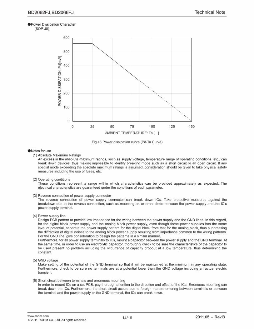
0
100
200
300
400
500
600
0 25 50 75 100 125 150
AMBIENT TEMPERATURE: Ta [ ]
PO
WE
R D
ISS
IPA
TIO
N: P
d[m
W]
Power Dissipation Character
(SOP-J8)
Fig.43 Power dissipation curve (Pd-Ta Curve)
Notes for use
(1) Absolute Maximum Ratings An excess in the absolute maximum ratings, such as supply voltage, temperature range of operating conditions, etc., can break down devices, thus making impossible to identify breaking mode such as a short circuit or an open circuit. If any special mode exceeding the absolute maximum ratings is assumed, consideration should be given to take physical safety measures including the use of fuses, etc.
(2) Operating conditions
These conditions represent a range within which characteristics can be provided approximately as expected. The electrical characteristics are guaranteed under the conditions of each parameter.
(3) Reverse connection of power supply connector
The reverse connection of power supply connector can break down ICs. Take protective measures against the breakdown due to the reverse connection, such as mounting an external diode between the power supply and the IC’s power supply terminal.
(4) Power supply line
Design PCB pattern to provide low impedance for the wiring between the power supply and the GND lines. In this regard, for the digital block power supply and the analog block power supply, even though these power supplies has the same level of potential, separate the power supply pattern for the digital block from that for the analog block, thus suppressing the diffraction of digital noises to the analog block power supply resulting from impedance common to the wiring patterns. For the GND line, give consideration to design the patterns in a similar manner. Furthermore, for all power supply terminals to ICs, mount a capacitor between the power supply and the GND terminal. At the same time, in order to use an electrolytic capacitor, thoroughly check to be sure the characteristics of the capacitor to be used present no problem including the occurrence of capacity dropout at a low temperature, thus determining the constant.
(5) GND voltage
Make setting of the potential of the GND terminal so that it will be maintained at the minimum in any operating state. Furthermore, check to be sure no terminals are at a potential lower than the GND voltage including an actual electric transient.
(6) Short circuit between terminals and erroneous mounting
In order to mount ICs on a set PCB, pay thorough attention to the direction and offset of the ICs. Erroneous mounting can break down the ICs. Furthermore, if a short circuit occurs due to foreign matters entering between terminals or between the terminal and the power supply or the GND terminal, the ICs can break down.
Technical Note
15/16
BD2062FJ,BD2066FJ
www.rohm.com 2011.05 - Rev.B© 2011 ROHM Co., Ltd. All rights reserved.
(7) Operation in strong electromagnetic field
Be noted that using ICs in the strong electromagnetic field can malfunction them. (8) Inspection with set PCB
On the inspection with the set PCB, if a capacitor is connected to a low-impedance IC terminal, the IC can suffer stress. Therefore, be sure to discharge from the set PCB by each process. Furthermore, in order to mount or dismount the set PCB to/from the jig for the inspection process, be sure to turn OFF the power supply and then mount the set PCB to the jig. After the completion of the inspection, be sure to turn OFF the power supply and then dismount it from the jig. In addition, for protection against static electricity, establish a ground for the assembly process and pay thorough attention to the transportation and the storage of the set PCB.
(9) Input terminals
In terms of the construction of IC, parasitic elements are inevitably formed in relation to potential. The operation of the parasitic element can cause interference with circuit operation, thus resulting in a malfunction and then breakdown of the input terminal. Therefore, pay thorough attention not to handle the input terminals, such as to apply to the input terminals a voltage lower than the GND respectively, so that any parasitic element will operate. Furthermore, do not apply a voltage to the input terminals when no power supply voltage is applied to the IC. In addition, even if the power supply voltage is applied, apply to the input terminals a voltage lower than the power supply voltage or within the guaranteed value of electrical characteristics.
(10) Ground wiring pattern
If small-signal GND and large-current GND are provided, It will be recommended to separate the large-current GND pattern from the small-signal GND pattern and establish a single ground at the reference point of the set PCB so that resistance to the wiring pattern and voltage fluctuations due to a large current will cause no fluctuations in voltages of the small-signal GND. Pay attention not to cause fluctuations in the GND wiring pattern of external parts as well.
(11) External capacitor
In order to use a ceramic capacitor as the external capacitor, determine the constant with consideration given to a degradation in the nominal capacitance due to DC bias and changes in the capacitance due to temperature, etc.
(12) Thermal shutdown circuit (TSD)
When junction temperatures become detected temperatures or higher, the thermal shutdown circuit operates and turns a switch OFF. The thermal shutdown circuit is aimed at isolating the LSI from thermal runaway as much as possible. Do not continuously use the LSI with this circuit operating or use the LSI assuming its operation.
(13) Thermal design
Perform thermal design in which there are adequate margins by taking into account the power dissipation (Pd) in actual states of use.
Technical Note
16/16
BD2062FJ,BD2066FJ
www.rohm.com 2011.05 - Rev.B© 2011 ROHM Co., Ltd. All rights reserved.
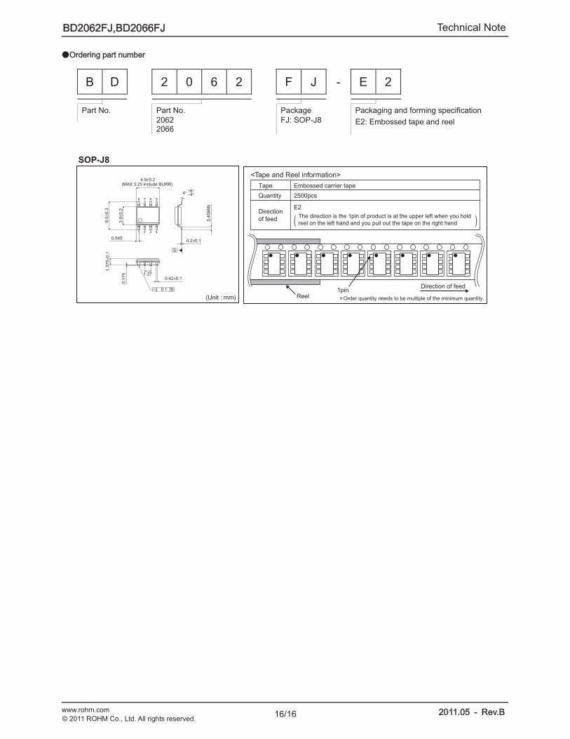
Ordering part number
B D 2 0 6 2 F J - E 2
Part No. Part No.
2062 2066
Package
FJ: SOP-J8
Packaging and forming specification
E2: Embossed tape and reel
∗ Order quantity needs to be multiple of the minimum quantity.
<Tape and Reel information>
Embossed carrier tapeTape
Quantity
Direction
of feedThe direction is the 1pin of product is at the upper left when you hold
reel on the left hand and you pull out the tape on the right hand
2500pcs
E2
( )
Direction of feed
Reel1pin
(Unit : mm)
SOP-J8
4°+6°−4°
0.2±0.1
0.4
5M
IN
2 3 4
5678
1
4.9±0.2
0.545
3.9
±0.2
6.0
±0.3
(MAX 5.25 include BURR)
0.42±0.11.27
0.1
75
1.3
75
±0.1
0.1 S
S
R1120Awww.rohm.com
© 2011 ROHM Co., Ltd. All rights reserved.
Notice
ROHM Customer Support System
http://www.rohm.com/contact/
Thank you for your accessing to ROHM product informations.
More detail product informations and catalogs are available, please contact us.
N o t e s
No copying or reproduction of this document, in part or in whole, is permitted without the
consent of ROHM Co.,Ltd.
The content speci?ed herein is subject to change for improvement without notice.
The content speci?ed herein is for the purpose of introducing ROHM's products (hereinafter
"Products"). If you wish to use any such Product, please be sure to refer to the speci?cations,
which can be obtained from ROHM upon request.
Examples of application circuits, circuit constants and any other information contained herein
illustrate the standard usage and operations of the Products. The peripheral conditions must
be taken into account when designing circuits for mass production.
Great care was taken in ensuring the accuracy of the information speci?ed in this document.
However, should you incur any damage arising from any inaccuracy or misprint of such
information, ROHM shall bear no responsibility for such damage.
The technical information speci?ed herein is intended only to show the typical functions of and
examples of application circuits for the Products. ROHM does not grant you, explicitly or
implicitly, any license to use or exercise intellectual property or other rights held by ROHM and
other parties. ROHM shall bear no responsibility whatsoever for any dispute arising from the
use of such technical information.
The Products speci?ed in this document are intended to be used with general-use electronic
equipment or devices (such as audio visual equipment, of?ce-automation equipment, commu-
nication devices, electronic appliances and amusement devices).
The Products speci?ed in this document are not designed to be radiation tolerant.
While ROHM always makes efforts to enhance the quality and reliability of its Products, a
Product may fail or malfunction for a variety of reasons.
Please be sure to implement in your equipment using the Products safety measures to guard
against the possibility of physical injury, ?re or any other damage caused in the event of the
failure of any Product, such as derating, redundancy, ?re control and fail-safe designs. ROHM
shall bear no responsibility whatsoever for your use of any Product outside of the prescribed
scope or not in accordance with the instruction manual.
The Products are not designed or manufactured to be used with any equipment, device or
system which requires an extremely high level of reliability the failure or malfunction of which
may result in a direct threat to human life or create a risk of human injury (such as a medical
instrument, transportation equipment, aerospace machinery, nuclear-reactor controller, fuel-
controller or other safety device). ROHM shall bear no responsibility in any way for use of any
of the Products for the above special purposes. If a Product is intended to be used for any
such special purpose, please contact a ROHM sales representative before purchasing.
If you intend to export or ship overseas any Product or technology speci?ed herein that may
be controlled under the Foreign Exchange and the Foreign Trade Law, you will be required to
obtain a license or permit under the Law.