powering the xilinx® zynq® 7015 fpga with … · tida-00551 - test reportpowering the xilinx®...
TRANSCRIPT

TIDA-00551 - Test ReportPowering the Xilinx® Zynq® 7015 FPGA with TPS659110 Power Management IC 1
Copyright © 2015, Texas Instruments Incorporated
TIDA-00551 Test Report
Powering the Xilinx® Zynq® 7015 FPGA with TPS659110 Power Management IC
TI Designs
TI Designs provide the foundation that you need including methodology, testing and design files to quickly evaluate and customize the system. TI Designs help you accelerate your time to market.
Design Resources
TIDA-00551 Design Folder
TPS65911x Product Folder
Report Contents
Block Diagram: TPS659110/Zynq® 7015
Efficiency Curves
Load Regulation Curves
Power-Up Sequence (No Load)
Output Ripple Voltage
Load Transients
Design Considerations
Feature Applications
Programmable Logic Controller (PLC)
Industrial Automation
Industrial PC
IP & Smart Cameras
Point of Sale
Description
This TPS659110-based reference design is a compact, integrated power solution for Xilinx® Zynq® 7015 SoC/FPGAs (out of the Zynq® 7000 series family of products). This design showcases TPS659110 as an all-in-one PMIC solution capable of supplying eight rails to power the Zynq® 7015 SoC/FPGAs. The total board area needed for TPS659110, including passive components, to supply the eight power rails to the Zynq® 7015 is just 2.095 in2. The TPS659110 has the flexibility to support both DDR3 and DDR3L memory. TPS659110 also has the ability to support the Zynq® 7010 FPGA as well. This power management IC can be run from a single 5V supply.
Ask The Analog Experts WEBENCH® Design Center
Figure 1 - Top Side
Figure 2 - Bottom Side

www.ti.com
TIDA-00551 - Test ReportPowering the Xilinx® Zynq® 7015 FPGA with TPS659110 Power Management IC 2
Copyright © 2015, Texas Instruments Incorporated
TPS659110/Zynq® 7015 Block Diagram (Return to Top) 5V Power Supply Block Diagram
Figure 3 – 5V Supply Diagram
CC
IN_BU DCDC6
Zynq® 7015TPS659110
SW1
SWIO
LDO5
VCC1
(VDD1_SMPS)
VCCIO
(VIO_SMPS)
VCC4
VCCPINT
VCCAUX
VCCO_1.8V
VCCO_MIO0/1
VCCPAUX
VCCPLL
VCCADC
VCCO_1.2V
MGTAVTT
1.0V @ 1.261A
1.8V @ 0.786A
1.2V @ 0.258A
5V Input
= Power Sequence Order
2
3
5
X
Note:
VCC5
VCC3
VCC3
VCCO_1.35V
VCCO_2.5V
VCCO_3.3V
LDO4
LDO6
LDO7
1.35V @ 0.015A
2.5V @ 0.002A
3.3V @ 0.050A
6
7
8
TPS659110 Zynq 7015 8 Watt Block Diagram
VOUTV5IN
(VDDCtrl)VCCINT
VCCBRAM
MGTAVCC
1.0V @ 4.42A
1
SW2VCC2
(VDD2_SMPS)VCCO_1.5V
VCCO_DDR
1.5V @ 0.747A
4

www.ti.com
TIDA-00551 – Test ReportPowering the Xilinx® Zynq® 7015 FPGA with TPS659110 Power Management IC 3
Copyright © 2015, Texas Instruments Incorporated
Typical Voltage and Current Requirements in 5V End Applications The table below highlights the typical current consumptions for the Zynq® 7015 seen in end applications.
Note: The current consumption numbers above are only estimates and the actual current consumption may vary depending on the application.
Test Specifications Testing was based on the below specifications
Zynq® 7015 Supply Rails Voltage Current Consumption (A)
VCCINT 1.0V 4.005
VCCPINT 1.0V 1.261
VCCBRAM 1.0V 0.052
MGTAVCC 1.0V 0.363
VCCO_1.2V 1.2V 0.039
MGTAVTT 1.2V 0.219
VCCO_1.35V 1.35V 0.015
VCCO_DDR 1.5V 0.463
VCCO_1.5V 1.5V 0.284
VCCAUX 1.8V 0.518
VCCPAUX 1.8V 0.073
VCCPLL 1.8V 0.015
VCCADC 1.8V 0.030
VCCO_1.8V 1.8V 0.050
VCCO_MIO0/1_1.8V 1.8V 0.050
VCCO_2.5V 2.5V 0.002
VCCO_3.3V 3.3V 0.050
Zynq® 7015 Supply Rails TPS659110 Rail Voltage Tolerance Transient
VDDCTRL
VCCBRAM
MGTAVCC
VCCPINT VDD1_SMPS 1.0V +/-5% 50% load ≤ 1A/us
VCCO_DDR
VCCO_1.5V
VCCAUX
VCCPAUX
VCCPLL
VCCADC
VCCO_1.8V
VCCO_MIO0/1_1.8V
50% load ≤ 1A/us
50% load ≤ 1A/us
VDD2_SMPS 1.5V +/-5%
VIO_SMPS +/-5%1.8V
VDDCTRL 50% load ≤ 1A/us+/-5%1.0V

www.ti.com
TIDA-00551 – Test ReportPowering the Xilinx® Zynq® 7015 FPGA with TPS659110 Power Management IC 4
Copyright © 2015, Texas Instruments Incorporated
Efficiency Curves (Return to Top) VDDCTRL (Vout=1.0V) – VCCINT, VCCBRAM, MGTAVCC
Figure 4 - VDDCTRL Efficiency @ 25C
VDD1_SMPS (Vout=1.0V) – VCCPINT
Figure 5 – VDD1 SMPS Efficiency @ 25C
0%
10%
20%
30%
40%
50%
60%
70%
80%
90%
100%
0.0 0.0 0.1 1.0 10.0
Eff
icie
ncy
Load Current (A)
VDDCTRL Efficiency vs Load Current @ Ta=25°C
PWM
Vin = 5.0V
Vout = 1.0V
0%
10%
20%
30%
40%
50%
60%
70%
80%
90%
100%
0.0 0.0 0.1 1.0 10.0
Eff
icie
nc
y
Load Current (A)
VDD1_SMPS Efficiency vs Load Current @ Ta=25°C
PWM PSM
Vin = 5.0V
Vout =
1.0V

www.ti.com
TIDA-00551 – Test ReportPowering the Xilinx® Zynq® 7015 FPGA with TPS659110 Power Management IC 5
Copyright © 2015, Texas Instruments Incorporated
VIO_SMPS (Vout=1.8V) – VCCAUX, VCCO_1.8V, VCCPAUX, VCCPLL, VCCO_MIO0/1, VCCADC
Figure 6 - DCDC2 Efficiency @ 25C
VDD2_SMPS (Vout=1.5V) – VCCO_DDR, VCCO_1.5V
Figure 7 - DCDC3 Efficiency @ 25C
0%
10%
20%
30%
40%
50%
60%
70%
80%
90%
100%
0.0 0.0 0.1 1.0 10.0
Eff
icie
ncy
Load Current (A)
VIO SMPS Efficiency vs Load Current @ Ta=25°C
PWM PSM
Vin = 5.0V
Vout = 1.8V
0%
10%
20%
30%
40%
50%
60%
70%
80%
90%
100%
0.0 0.0 0.1 1.0 10.0
Eff
icie
nc
y
Load Current (A)
VDD2 SMPS Efficiency vs Load Current @ Ta=25°C
PWM PSM
Vin = 5.0V
Vout = 1.5V

www.ti.com
TIDA-00551 – Test ReportPowering the Xilinx® Zynq® 7015 FPGA with TPS659110 Power Management IC 6
Copyright © 2015, Texas Instruments Incorporated
Load Regulation (Return to Top)
VDDCTRL (Vout=1.0V) – VCCINT, VCCBRAM
Figure 8 – VDDCTRL Load Regulation @ Ta=25
VDD1_SMPS (Vout=1.0V) – VCCPINT
Figure 9 – VDD1_SMPS Load Regulation @ Ta=25C
-3.00%
-2.00%
-1.00%
0.00%
1.00%
2.00%
3.00%
0.0 0.0 0.1 1.0 10.0
Lo
ad
Reg
ula
tio
n
Load Current (A)
VDDCTRL Load Regulation @ Ta=25°C
PWMVin = 5.0V
Vout = 1.0V
-3%
-2%
-1%
0%
1%
2%
3%
0.0 0.0 0.1 1.0 10.0
Lo
ad
Reg
ula
tio
n
Load Current (A)
VDD1_SMPS Load Regulation @ Ta=25°C
PWM PSM
Vin = 5.0V
Vout = 1.0V

www.ti.com
TIDA-00551 – Test ReportPowering the Xilinx® Zynq® 7015 FPGA with TPS659110 Power Management IC 7
Copyright © 2015, Texas Instruments Incorporated
VIO_SMPS (Vout=1.8V) – VCCAUX, VCCO_1.8V, VCCPAUX, VCCPLL, VCCO_MIO0/1, VCCADC
Figure 10 - VIO SMPS Load Regulation @ Ta=25C
VDD2_SMPS (Vout=1.5V) – VCCO_DDR, VCCO_1.5V
Figure 11 - VDD2 SMPS Load Regulation @ Ta=25C
-3%
-2%
-1%
0%
1%
2%
3%
0.0 0.0 0.1 1.0 10.0
Lo
ad
Re
gu
lati
on
Load Current (A)
VIO SMPS Load Regulation @ Ta=25°C
PWM PSM
Vin = 5.0V
Vout = 1.8V
-3%
-2%
-1%
0%
1%
2%
3%
0.0 0.0 0.1 1.0 10.0
Lo
ad
Reg
ula
tio
n
Load Current (A)
VDD2 SMPS Load Regulation @ Ta=25°C
PWM PSM
Vin = 5.0V
Vout = 1.5V

www.ti.com
TIDA-00551 – Test ReportPowering the Xilinx® Zynq® 7015 FPGA with TPS659110 Power Management IC 8
Copyright © 2015, Texas Instruments Incorporated
Power-Up Sequence (No Load) (Return to Top)
Timing Waveforms
Figure 12 – Power-Up Sequence (No Load) Timing Waveforms
Voltage Waveforms
Startup Timing

www.ti.com
TIDA-00551 – Test ReportPowering the Xilinx® Zynq® 7015 FPGA with TPS659110 Power Management IC 9
Copyright © 2015, Texas Instruments Incorporated
Figure 13 – Power-Up Sequence (No Load) Timing Waveforms
(VCCINT_1.0V, VCCPINT_1.0V, VCCAUX_1.8V, VCCO_DDR_1.5V)
Figure 14 – Power-Up Sequence (No Load) Voltage Waveforms
(VCCO_1.2V, VCCO_1.35V, VCCO_2.5V, VCCO_3.3V)

www.ti.com
TIDA-00551 – Test ReportPowering the Xilinx® Zynq® 7015 FPGA with TPS659110 Power Management IC 10
Copyright © 2015, Texas Instruments Incorporated
Output Ripple Voltage (Full Load) (Return to Top)
VDDCTRL (Vout = 1V) – VCCPINT (Typical Max Load)
VDD1_SMPS (Vout = 1V) – VCCPINT (Typical Max Load)
Figure 16 - VCCPINT Vripple Voltage
Figure 15 - VCCPINT Ripple Voltage

www.ti.com
TIDA-00551 – Test ReportPowering the Xilinx® Zynq® 7015 FPGA with TPS659110 Power Management IC 11
Copyright © 2015, Texas Instruments Incorporated
VDD2_SMPS (Vout = 1.5V) – VCCO_DDR, VCCO_1.5V (Typical Max Load)
Figure 17 - VDD2 SMPS Vripple Voltage
VIO_SMPS (Vout = 1.8V) – VCCAUX, VCCO_1.8V, VCCPAUX, VCCPLL, VCCO_MIO0/1, VCCADC (Typical Max Load)
Figure 18 - VIO SMPS Vripple Voltage

www.ti.com
TIDA-00551 – Test ReportPowering the Xilinx® Zynq® 7015 FPGA with TPS659110 Power Management IC 12
Copyright © 2015, Texas Instruments Incorporated
Load Transients (Return to Top)
Load transients for each of the DC-DC converters were completed by applying a load step of 50mA to at least 50% of the max load for the converter under test. The slew rate of each of the transients is ≤ 1A/us.
VDDCTRL (Vout = 1V) – VCCINT, VCCBRAM, MGTAVCC Load Step (100mA to 2.35A, 1A/1us)
VDD1_SMPS (Vout = 1V) – VCCPINT Load Step (50mA to 700mA, 1A/1us)

www.ti.com
TIDA-00551 – Test ReportPowering the Xilinx® Zynq® 7015 FPGA with TPS659110 Power Management IC 13
Copyright © 2015, Texas Instruments Incorporated
VDD2_SMPS (Vout = 1.5V) – VCCO_DDR, VCCO_1.5V Load Step (50mA to 624mA, 1A/1us)
VIO_SMPS (Vout = 1.8V) – VCCAUX, VCCO_1.8V, VCCPAUX, VCCPLL, VCCO_MIO0/1, VCCADC (50mA to 450mA, 1A/us)

www.ti.com
TIDA-00551 – Test ReportPowering the Xilinx® Zynq® 7015 FPGA with TPS659110 Power Management IC 14
Copyright © 2015, Texas Instruments Incorporated
Design Considerations (Return to Top)
Xilinx® Zynq® 7010/15 Recommended Power Up/Down Sequencing For reference, the sequencing requirements from the Xilinx Zynq 7010/15 datasheet are shown below:
PS Power-On/Off Power Supply Sequencing The recommended power-on sequence is VCCPINT, VCCPAUX, and VCCPLL together, then the PS VCCO supplies (VCCO_MIO0, VCCO_MIO1, and VCCO_DDR) to achieve minimum current draw and ensure that the I/Os are 3-stated at power-on. The recommended power-off sequence is the reverse of the power-on sequence. If VCCPAUX, VCCPLL, and the PS VCCO supplies (VCCO_MIO0, VCCO_MIO1, and VCCO_DDR) have the same recommended voltage levels, then they can be powered by the same supply and ramped simultaneously. Xilinx recommends powering VCCPLL with the same supply as VCCPAUX, with an optional ferrite bead filter. For VCCO_MIO0 and VCCO_MIO1 voltages of 3.3V:
The voltage difference between VCCO_MIO0 /VCCO_MIO1 and VCCPAUX must not exceed 2.625V for longer than TVCCO2VCCAUX for each power-on/off cycle to maintain device reliability levels.
The TVCCO2VCCAUX time can be allocated in any percentage between the power-on and power-off ramps.
PL Power-On/Off Power Supply Sequencing
The recommended power-on sequence for the PL is VCCINT, VCCBRAM, VCCAUX, and VCCO to achieve minimum current draw and ensure that the I/Os are 3-stated at power-on. The recommended power-off sequence is the reverse of the power-on sequence. If VCCINT and VCCBRAM have the same recommended voltage levels then both can be powered by the same supply and ramped simultaneously. If VCCAUX and VCCO have the same recommended voltage levels then both can be powered by the same supply and ramped simultaneously. For VCCO voltages of 3.3V in HR I/O banks and configuration bank 0:
The voltage difference between VCCO and VCCAUX must not exceed 2.625V for longer than TVCCO2VCCAUX for each power-on/off cycle to maintain device reliability levels.
The TVCCO2VCCAUX time can be allocated in any percentage between the power-on and power-off ramps.
GTP Transceivers (XC7Z015 Only) The recommended power-on sequence to achieve minimum current draw for the GTP transceivers (XC7Z015 only) is VCCINT, VMGTAVCC, VMGTAVTT OR VMGTAVCC, VCCINT, VMGTAVTT. Both VMGTAVCC and VCCINT can be ramped simultaneously. The recommended power-off sequence is the reverse of the power-on sequence to achieve minimum current draw.
www.ti.com
TIDA-00551 – Test ReportPowering the Xilinx® Zynq® 7015 FPGA with TPS659110 Power Management IC 15
Copyright © 2015, Texas Instruments Incorporated
If these recommended sequences are not met, current drawn from VMGTAVTT can be higher than specifications during power-up and power-down.
When VMGTAVTT is powered before VMGTAVCC and VMGTAVTT – VMGTAVCC > 150 mV and VMGTAVCC < 0.7V, the VMGTAVTT current draw can increase by 460 mA per transceiver during VMGTAVCC ramp up. The duration of the current draw can be up to 0.3 x TMGTAVCC (ramp time from GND to 90% of VMGTAVCC). The reverse is true for power-down.
When VMGTAVTT is powered before VCCINT and VMGTAVTT – VCCINT > 150 mV and VCCINT < 0.7V, the VMGTAVTT current draw can increase by 50 mA per transceiver during VCCINT ramp up. The duration of the current draw can be up to 0.3 x TVCCINT (ramp time from GND to 90% of VCCINT). The reverse is true for power-down.
There is no recommended sequence for supplies not shown.
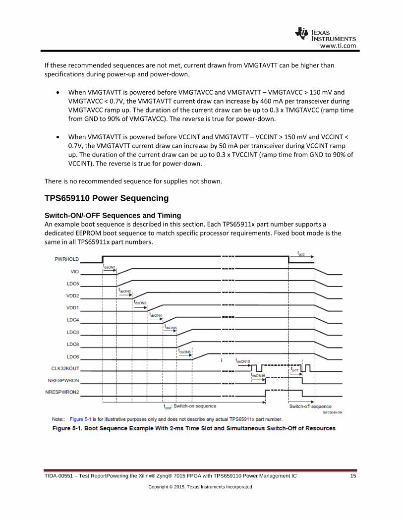
TPS659110 Power Sequencing Switch-ON/-OFF Sequences and Timing
An example boot sequence is described in this section. Each TPS65911x part number supports a dedicated EEPROM boot sequence to match specific processor requirements. Fixed boot mode is the same in all TPS65911x part numbers.

www.ti.com
TIDA-00551 – Test ReportPowering the Xilinx® Zynq® 7015 FPGA with TPS659110 Power Management IC 16
Copyright © 2015, Texas Instruments Incorporated
BOOT Configuration and Switch-ON/-OFF Sequences The power sequence is the automated switch-on of the devices resources when an OFF-to-ACTIVE transition occurs. The power-on sequence has 15 sequential time slots to which resources (DC-DC converters, LDOs, 32-kHz clock, GPIO0, GPIO2, GPIO6, GPIO7) can be assigned. The time slot length can be selected to be 0.5 ms or 2 ms. If a resource is not assigned to any time slot, it will be in off mode after the power-on sequence and the voltage level can be changed through the register SEL bits before enabling the resource. Power off disables all power resources at the same time by default. By setting the PWR_OFF_SEQ control bit to 1, power off will follow the power-up sequence in reverse order (the first resource to be powered on will be last to power off). The values of VDD1, VDD2, and VDDCtrl set in the boot sequence can be selected from 16 steps. For the whole range, 100-mV steps are available: 0.6/0.7...1.4/1.5 V. From 0.8 to 1.4 V, additional values with 50- mV step resolution can be set: 0.85/1.05...1.35 V. For LDO1, LDO2, and LDO4 all levels from 1.0 to 3.3 V are selectable in the boot sequence with 50-mV steps. For other LDOs, the level is selectable with 100-mV steps, from 1.0 to 3.3 V. The device supports three boot configurations, which define the power sequence and several device control bits. The boot configuration is selectable by the device BOOT1 pin.
The BOOT1 input pad is disabled after the boot mode is read at power up, to save power. Table 6-2 and Table 6-3 describe the power sequence and general control bits defined in the boot sequence, respectively. Fixed boot mode is the same in all part numbers while EEPROM boot mode is different in each part number. For EEPROM boot mode description refer to the User Guide for the selected part number. Control Signals SLEEP When none of the device SLEEP-disable conditions are met, a falling edge (default, or rising edge, depending on the programmed polarity) of this signal causes an ACTIVE-to-SLEEP state transition of the device. A rising edge (default, or falling edge, depending on the programmed polarity) causes a transition back to the ACTIVE state. This input signal is level-sensitive and no debouncing is applied. While the device is in the SLEEP state, predefined resources are automatically set in their low-power mode or off. Resources can be kept in their active mode (full-load capability) by programming the SLEEP_KEEP_LDO_ON and the SLEEP_KEEP_RES_ON registers. These registers contain 1 bit per power resource. If the bit is set to 1, then that resource stays in active mode when the device is in the SLEEP state. 32KCLKOUT is also included in the SLEEP_KEEP_RES_ON register and the 32-kHz clock output is maintained in the SLEEP state if the corresponding mask bit is set. The status (low or high) of GPO0, GPO6, GPO7, and GPO8 are also controlled by the SLEEP signal, to allow enabling and disabling of external resources during sleep.

www.ti.com
TIDA-00551 – Test ReportPowering the Xilinx® Zynq® 7015 FPGA with TPS659110 Power Management IC 17
Copyright © 2015, Texas Instruments Incorporated
PWRHOLD The PWRHOLD pin can be used as a PWRHOLD signal input or as a general purpose input (GPI). The mode is selected by the AUTODEV_ON bit, which is part of the boot configuration. When AUTODEV_MODE = 0, the PWRHOLD feature is selected. Configured as PWRHOLD, when none of the device POWER ON disable conditions are met, a high level of this signal causes an OFF-to-ACTIVE state transition of the device and a low level causes a transition back to the OFF state. This input signal is level-sensitive and no debouncing is applied. The rising and/or falling edge of PWRHOLD is highlighted through an associated interrupt if interrupt is unmasked. When AUTODEV_ON = 1, the pin is used as a GPI. As a GPI, this input can generate a mask able interrupt from a rising or falling edge of the input. When AUTODEV_ON = 1, a rising edge of NRESPWRON also automatically sets the DEV_ON bit to 1 to maintain supplies after the switch-on sequence, thus removing the need for the processor to set the PWRHOLD signal or the DEV_ON bit. BOOT1 This signal determines with which processor the device is working and, hence, which power-up sequence is needed. For more details, see Section 5.23.1 in the datasheet. There is no debouncing on this input signal. NRESPWRON, NRESPWRON2 The NRESPWRON signal is used as the reset to the processor and is in the VDDIO domain. It is held low until the ACTIVE state is reached. See Section 5.23.1 in the datasheet to get detailed timing. The NRESPWRON2 signal is a second reset output. It follows the state of NRESPWRON but has an open-drain output with external pull-up. The supply for the external pull-up must not be activated before the TPS65911 device is in control of the output state (that is, not earlier than during first power-up sequence slot). In off mode, the NRESPWRON2 output has weak internal pulldown. CLK32KOUT This signal is the output of the 32K oscillator, which can be enabled or not during the power-on sequence, depending on the boot mode. It can be enabled and disabled by register bit, during the ACTIVE state of the device. The CLK32KOUT output can also be enabled or not during the SLEEP state of the device depending on the programming of the SLEEPMASK register. PWRON
The PWRON input is connected to an external button. If the device is in the OFF or SLEEP state, a debounced falling edge (PWRON input low for minimum of 100 ms) causes an OFF-to-ACTIVE state or a SLEEP-to-ACTIVE state transition of the device. If the device is in active mode, then a low level on this signal generates an interrupt. If the PWRON signal is low for more than the PWON_TO_OFF_DELAY delay and the corresponding interrupt is not acknowledged by the processor within 1 second, the device goes into the OFF state. See Figure 5-2 and Figure 5-3 in the datasheet for PWRON behavior. INT1 The INT1 signal (default active low) warns the host processor of any event that has occurred on the TPS65911 device. The host processor can then poll the interrupt from the interrupt status register through I2C to identify the interrupt source. A low level (default setting) indicates an active interrupt, highlighted in the INT_STS_REG register. The polarity of INT1 can be set programming the IT_POL control bit. INT1 flag active is a POWER ON enable condition during a fixed delay, tDOINT1 (only), when the device is in the OFF state (when NRESPWRON is low).

www.ti.com
TIDA-00551 – Test ReportPowering the Xilinx® Zynq® 7015 FPGA with TPS659110 Power Management IC 18
Copyright © 2015, Texas Instruments Incorporated
Any of the interrupt sources can be masked programming the INT_MSK_REG register. When an interrupt is masked its corresponding interrupt status bit is still updated, but the INT1 flag is not activated. Interrupt source masking can be used to mask a device switch-on event. Because interrupt flag active is a POWER ON enable condition, during tDOINT1 delay, any interrupt not masked must be cleared to allow immediate turn off of the device. For a description of interrupt sources, see table 6-5 in the datasheet. EN2 and EN1 EN2 and EN1 are the data and clock signals of the serial control interface dedicated to voltage scaling applications. These signals can also be programmed to be used as enable signals of one or several supplies, when the device is on (NRESPWRON high). A resource assigned to EN2 or EN1 control automatically disables the serial control interface. Programming EN1_LDO_ASS_REG, EN2_LDO_REG, and SLEEP_KEEP_LDO_ON_REG registers: EN1 and EN2 signals can be used to control the turn on/off or SLEEP state of any LDO-type supplies. Programming EN1_SMPS_ASS_REG, EN2_SMPS_ASS_REG, and SLEEP_KEEP_RES_ON registers: EN1 and EN2 signals can be used to control the turn on/off or LOW-POWER state (PFM mode) of SMPS type supplies. The EN2 and EN1 signals can be used to set the output voltage of VDD1 and VDD2 SMPS from a roof to a floor value, preprogrammed in the VDD1_OP_REG, VDD2_OP_REG and VDD1_SR_REG, VDD2_SR_REG registers. When a supply is controlled through the EN1 or EN2 signals, its state is no longer driven by the device SLEEP state. GPIO0 to GPIO8 GPIO0, GPIO2, GPIO6, and GPIO7 can be programmed to be part of the power-up sequence and used as enable signals for external resources. GPIO0 is a configurable I/O in the VCC7 domain. By default, its output is push-pull, driving low. GPIO0 can also be configured as an open-drain output with external pullup. GPIO1 through GPIO8 are configurable open-drain digital I/Os in the VRTC domain. GPIO directivity, debouncing delay, and internal pullup can be programmed. By default, all are inputs with weak internal pulldown; as open-drain output an external pullup is required. GPIO0, GPIO1, and GPIO3 through GPIO5 can be used to turn on the device if the corresponding interrupt is not masked. When configured as an input, GPIO2 cannot be used to turn on the device, even if its associated interrupt is not masked. The GPIO interrupt is level sensitive. When an interrupt is detected, before clearing the interrupt, it should first be disabled by masking it. GPIO1 and GPIO3, which have current sink capability of 10 mA, can also be used to drive LEDs connected to a 5-V supply. GPIO2 can be used for synchronizing DC-DC converters to an external clock. Programming DCDCCKEXT = 1, VDD1, VDD2, and VIO DCDC switching can be synchronized using a 3-MHz clock set though the GPIO2 pin. VDD1 and VDD2 will be in-phase and VIO will be phase shifted by 180 degrees. It is recommended not to connect noisy switching signals to GPIO4 and GPIO5.

www.ti.com
TIDA-00551 – Test ReportPowering the Xilinx® Zynq® 7015 FPGA with TPS659110 Power Management IC 19
Copyright © 2015, Texas Instruments Incorporated
HDRST Input HDRST is a cold reset input for the PMIC. High level at input forces the TPS65911 into off mode, causing a general reset of device to the default settings. The default state is defined by the register reset state and boot configuration. HDRST high level keeps the device in off mode. When reset is released and HDRST input goes low, the device automatically transitions to active mode. The device is kept in active mode for the period tDONIT1, after which another power-on enable reason is needed to maintain the device on. The HDRST input is in the VRTC domain and has a weak internal pulldown, which is active by default. PWRDN The PWRDN input is a reset input with selectable polarity (PWRDN_POL). High(low) level at input forces the TPS65911 device into off mode, causing a power-off reset. Off mode is maintained until PWRDN is released and a start-up reason like PWRON button press or DEV_ON = 1 is detected. An interrupt is generated to indicate the cause for shutdown. The PWRDN input is in the VRTC domain, but can tolerate a 5-V input. Comparators: COMP1 and COMP2 The TPS65911 device has three comparators for system status detection/control. One comparator detects the voltage at pin VCC7. When VCC7 > VMBHI, the comparator initiates a NO SUPPLY-to-OFF transition and the VMBHI_IT interrupt is generated. When VCC7 < VMBLO, the comparator initiates an ACTIVE/SLEEP/OFF-to-BACKUP transition. When both VCC7 and backup battery are below VBPNR, the NO SUPPLY state is entered. Comparators COMP1 and COMP2 detect the voltage of VCCS. Programmable comparator COMP1 is intended for detecting if battery voltage is high enough for an OFF-to-ACTIVE transition of the TPS65911 device. For an OFF-to-ACTIVE transition VCCS must be > VMBCH (main battery charged) and a level below the comparator threshold prevents the power-up sequence. The threshold can be set from 2.5 to 3.5 V with 50-mV steps through VMBCH_SEL. The comparator has debouncing so that VCCS must stay above VMBDCH (VMBCH – 0.1 V) for a debouncing period of 61 μs. The comparator can be bypassed if the threshold selection is set to 0. The default threshold is set in the boot configuration. In a system with a multiple-cell battery, the battery level is sensed through an external resistor divider. The TPS65911 device has an internal buffer at the VCCS input, which must be used with the external resistive divider. In a single-cell system, VCCS and VCC7 are connected directly to the battery. The VCCS input buffer can be bypassed to minimize power consumption. The buffer bypass is controlled with the VMBBUF_BYPASS bit in the boot configuration. COMP2 is disabled by default and can be enabled by software. The comparator trigger generates an interrupt which is programmable on the rising (VMBCH2_H_IT) or falling edge (VMBCH2_L_IT), hence the comparator can be used for detecting high or low battery scenarios. COMP2 generates an interrupt for the host. In sleep mode, this creates a wake-up interrupt for the host. In off mode, the comparator trigger generates a turn-on event. In backup or no supply modes, the comparator is not active.
The COMP2 threshold can be set from 2.5 to 3.5 V with 50-mV steps. Enabling the comparator is done through the voltage threshold selection bit VMBDCH2_SEL, which is set to 0 by default. I2C Interface A general-purpose serial control interface (CTL-I2C) allows read and write access to the configuration registers of all resources of the system. A second serial control interface (optional mode for EN1 and EN2 pins) can be dedicated to DVFS.

www.ti.com
TIDA-00551 – Test ReportPowering the Xilinx® Zynq® 7015 FPGA with TPS659110 Power Management IC 20
Copyright © 2015, Texas Instruments Incorporated
Both control interfaces are compliant with the HS-I2C specification. These interfaces support the standard slave mode (100 Kbps), fast mode (400 Kbps), and high-speed mode (3.4 Mbps). The general-purpose I2C module using one slave hard-coded address (ID1 = 2Dh). The voltage scaling dedicated I2C module uses one slave hard-coded address (ID0 = 12h). The master mode is not supported. Real-Time Clock (RTC) The RTC, which is driven by the 32-kHz clock, provides the alarm and timekeeping functions. The RTC is kept supplied when the device is in the OFF or the BACKUP state. The main functions of the RTC block are:
Time information (seconds/minutes/hours) directly in binary-coded decimal (BCD) format
Calendar information (Day/Month/Year/Day of the week) directly in BCD code up to year 2099
Programmable interrupts generation: The RTC can generate two interrupts: a timer interrupt RTC_PERIOD_IT periodically (1s/1m/1h/1d period) and an alarm interrupt RTC_ALARM_IT at a precise time of the day (alarm function). These interrupts are enabled using IT_ALARM and IT_TIMER control bits. Periodically interrupts can be masked during the SLEEP period to avoid host interruption and are automatically unmasked after SLEEP wakeup (using the IT_SLEEP_MASK_EN control bit).
Oscillator frequency calibration and time correction Thermal Monitoring and Shutdown A thermal protection module monitors the junction temperature of the device versus two thresholds:
Hot-die temperature threshold
Thermal shutdown temperature threshold When the hot-die temperature threshold is reached, an interrupt is sent to software to close the noncritical running tasks. When the thermal shutdown temperature threshold is reached, the TPS65911 device is set under reset and a transition to OFF state is initiated. Then the POWER ON enable conditions of the device are not considered until the die temperature has decreased below the hot-die threshold. Hysteresis is applied to the hot-die and shutdown thresholds, when detecting a falling edge of temperature, and both detections are debounced to avoid any parasitic detection. The TPS65911 device allows programming of four hot-die temperature thresholds to increase the flexibility of the system. By default, the thermal protection is enabled in ACTIVE state, but can be disabled through programming the THERM_REG register. The thermal protection can be enabled in SLEEP state programming the SLEEP_KEEP_RES_ON register. The thermal protection is automatically enabled during an OFF-to- ACTIVE state transition and is kept enabled in OFF state after a switch-off sequence caused by a thermal shutdown event. Transition to OFF state sequence caused by a thermal shutdown event is highlighted in the INT_STS_REG status register. Recovery from this OFF state is initiated (switch-on sequence) when the die temperature falls below the hot-die temperature threshold.

www.ti.com
TIDA-00551 – Test ReportPowering the Xilinx® Zynq® 7015 FPGA with TPS659110 Power Management IC 21
Copyright © 2015, Texas Instruments Incorporated
Hot-die and thermal shutdown temperature threshold detection states can be monitored or masked by reading or programming the THERM_REG register. The hot-die interrupt can be masked by programming the INT_MSK_REG register.

www.ti.com
TIDA-00551 - Test ReportPowering the Xilinx® Zynq® 7015 FPGA with TPS659110 Power Management IC 22
Copyright © 2015, Texas Instruments Incorporated
BGA Package Information

IMPORTANT NOTICE FOR TI REFERENCE DESIGNS
Texas Instruments Incorporated ("TI") reference designs are solely intended to assist designers (“Buyers”) who are developing systems thatincorporate TI semiconductor products (also referred to herein as “components”). Buyer understands and agrees that Buyer remainsresponsible for using its independent analysis, evaluation and judgment in designing Buyer’s systems and products.TI reference designs have been created using standard laboratory conditions and engineering practices. TI has not conducted anytesting other than that specifically described in the published documentation for a particular reference design. TI may makecorrections, enhancements, improvements and other changes to its reference designs.Buyers are authorized to use TI reference designs with the TI component(s) identified in each particular reference design and to modify thereference design in the development of their end products. HOWEVER, NO OTHER LICENSE, EXPRESS OR IMPLIED, BY ESTOPPELOR OTHERWISE TO ANY OTHER TI INTELLECTUAL PROPERTY RIGHT, AND NO LICENSE TO ANY THIRD PARTY TECHNOLOGYOR INTELLECTUAL PROPERTY RIGHT, IS GRANTED HEREIN, including but not limited to any patent right, copyright, mask work right,or other intellectual property right relating to any combination, machine, or process in which TI components or services are used.Information published by TI regarding third-party products or services does not constitute a license to use such products or services, or awarranty or endorsement thereof. Use of such information may require a license from a third party under the patents or other intellectualproperty of the third party, or a license from TI under the patents or other intellectual property of TI.TI REFERENCE DESIGNS ARE PROVIDED "AS IS". TI MAKES NO WARRANTIES OR REPRESENTATIONS WITH REGARD TO THEREFERENCE DESIGNS OR USE OF THE REFERENCE DESIGNS, EXPRESS, IMPLIED OR STATUTORY, INCLUDING ACCURACY ORCOMPLETENESS. TI DISCLAIMS ANY WARRANTY OF TITLE AND ANY IMPLIED WARRANTIES OF MERCHANTABILITY, FITNESSFOR A PARTICULAR PURPOSE, QUIET ENJOYMENT, QUIET POSSESSION, AND NON-INFRINGEMENT OF ANY THIRD PARTYINTELLECTUAL PROPERTY RIGHTS WITH REGARD TO TI REFERENCE DESIGNS OR USE THEREOF. TI SHALL NOT BE LIABLEFOR AND SHALL NOT DEFEND OR INDEMNIFY BUYERS AGAINST ANY THIRD PARTY INFRINGEMENT CLAIM THAT RELATES TOOR IS BASED ON A COMBINATION OF COMPONENTS PROVIDED IN A TI REFERENCE DESIGN. IN NO EVENT SHALL TI BELIABLE FOR ANY ACTUAL, SPECIAL, INCIDENTAL, CONSEQUENTIAL OR INDIRECT DAMAGES, HOWEVER CAUSED, ON ANYTHEORY OF LIABILITY AND WHETHER OR NOT TI HAS BEEN ADVISED OF THE POSSIBILITY OF SUCH DAMAGES, ARISING INANY WAY OUT OF TI REFERENCE DESIGNS OR BUYER’S USE OF TI REFERENCE DESIGNS.TI reserves the right to make corrections, enhancements, improvements and other changes to its semiconductor products and services perJESD46, latest issue, and to discontinue any product or service per JESD48, latest issue. Buyers should obtain the latest relevantinformation before placing orders and should verify that such information is current and complete. All semiconductor products are soldsubject to TI’s terms and conditions of sale supplied at the time of order acknowledgment.TI warrants performance of its components to the specifications applicable at the time of sale, in accordance with the warranty in TI’s termsand conditions of sale of semiconductor products. Testing and other quality control techniques for TI components are used to the extent TIdeems necessary to support this warranty. Except where mandated by applicable law, testing of all parameters of each component is notnecessarily performed.TI assumes no liability for applications assistance or the design of Buyers’ products. Buyers are responsible for their products andapplications using TI components. To minimize the risks associated with Buyers’ products and applications, Buyers should provideadequate design and operating safeguards.Reproduction of significant portions of TI information in TI data books, data sheets or reference designs is permissible only if reproduction iswithout alteration and is accompanied by all associated warranties, conditions, limitations, and notices. TI is not responsible or liable forsuch altered documentation. Information of third parties may be subject to additional restrictions.Buyer acknowledges and agrees that it is solely responsible for compliance with all legal, regulatory and safety-related requirementsconcerning its products, and any use of TI components in its applications, notwithstanding any applications-related information or supportthat may be provided by TI. Buyer represents and agrees that it has all the necessary expertise to create and implement safeguards thatanticipate dangerous failures, monitor failures and their consequences, lessen the likelihood of dangerous failures and take appropriateremedial actions. Buyer will fully indemnify TI and its representatives against any damages arising out of the use of any TI components inBuyer’s safety-critical applications.In some cases, TI components may be promoted specifically to facilitate safety-related applications. With such components, TI’s goal is tohelp enable customers to design and create their own end-product solutions that meet applicable functional safety standards andrequirements. Nonetheless, such components are subject to these terms.No TI components are authorized for use in FDA Class III (or similar life-critical medical equipment) unless authorized officers of the partieshave executed an agreement specifically governing such use.Only those TI components that TI has specifically designated as military grade or “enhanced plastic” are designed and intended for use inmilitary/aerospace applications or environments. Buyer acknowledges and agrees that any military or aerospace use of TI components thathave not been so designated is solely at Buyer's risk, and Buyer is solely responsible for compliance with all legal and regulatoryrequirements in connection with such use.TI has specifically designated certain components as meeting ISO/TS16949 requirements, mainly for automotive use. In any case of use ofnon-designated products, TI will not be responsible for any failure to meet ISO/TS16949.IMPORTANT NOTICE
Mailing Address: Texas Instruments, Post Office Box 655303, Dallas, Texas 75265Copyright © 2015, Texas Instruments Incorporated