power/performance based scalability comparisons
TRANSCRIPT
Power/Performance Based Scalability Comparisons betweenConventional and Novel Transistors Down to 32nm Technology Node
P. Kapur, R. S. Shenoy, and K. C. SaraswatCenter for Integrated Systems (CIS) 1 10
Stanford UniversityStanford, CA 94305 U.S.A
kapurpgstanford.edu
Abstract -- We quantify and compare the scalability of bulk,partially depleted SOI, and double gate transistors with andwithout high-k gate dielectric down to 32nm technology node interms of globally optimized power/performance curves. Thenovelty of work is in that it provides a quantitative tool todetermine the suitable insertion point for novel transistorschemes. It also addresses optimum supply/threshold voltage, gatedielectric thickness, and doping concentration scaling, unique todifferent devices and circuit functional blocks.
I. INTRODUCTIONScaling-induced dramatic rise in leakage power [1] has
prompted aggressive search for solutions, which mitigate thisproblem at different levels including architecture, circuits anddevices. In the area of devices, this has led to an explosion ofnovel ideas in the structural (e.g. multi-gate FETs) andmaterials domain (e.g. high-k gate dielectric). A faircomparison of the efficacy of these solutions at future nodes,and their advantages over the currently prevalent Bulk/SiO2gate transistor requires a comprehensive comparisonmethodology. In this work, we develop this standard usingglobally optimized power/performance curves. A uniquepower/performance curve for each type of device is obtainedby a multi-dimensional optimization of supply and thresholdvoltage (Vdd, Vt), doping concentration (Na), and equivalentoxide thickness (EOT) for gate dielectric. The methodologycan serve as a powerful tool for device and circuits communityby aiding in 1) Device selection at future nodes with no SPICEmodels, 2) Optimum device design once appropriate device isselected, 3) predicting Vdd scaling trends for differentfunctional blocks depending on the device selection.
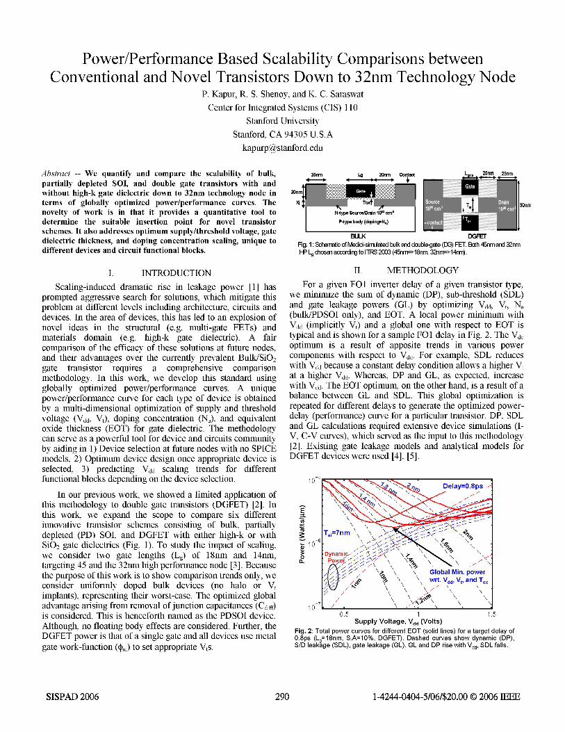
In our previous work, we showed a limited application ofthis methodology to double gate transistors (DGFET) [2]. Inthis work, we expand the scope to compare six differentinnovative transistor schemes consisting of bulk, partiallydepleted (PD) SOI, and DGFET with either high-k or withSiO2 gate dielectrics (Fig. 1). To study the impact of scaling,we consider two gate lengths (Lg) of 18nm and 14nm,targeting 45 and the 32nm high performance node [3]. Becausethe purpose of this work is to show comparison trends only, weconsider uniformly doped bulk devices (no halo or Vtimplants), representing their worst-case. The optimized globaladvantage arising from removal ofjunction capacitances (Cdiff)is considered. This is henceforth named as the PDSOI device.Although, no floating body effects are considered. Further, theDGFET power is that of a single gate and all devices use metalgate work-function (Om) to set appropriate Vts.
25nm Lg 20nm Contacti------'. 4 0-4
20nr
N-type Source/Drain 102 cnmP-type body (doping=NA)
BULK DGFErFig. 1: Schematic ofMedid-sirrulated bulk and double-gate (DG) FET. Both 45nm and 32nmHP b chosen acoording to ITRS 2003 (45nmn>18nnR 32nmn>14nm).
II. METHODOLOGYFor a given FOI inverter delay of a given transistor type,
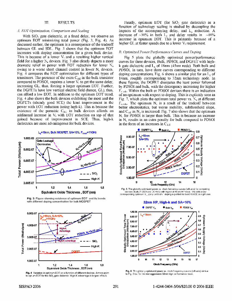
we minimize the sum of dynamic (DP), sub-threshold (SDL)and gate leakage powers (GL) by optimizing Vdd, Vt, Na(bulk/PDSOI only), and EOT. A local power minimum withVdd (implicitly Vt) and a global one with respect to EOT istypical and is shown for a sample FO1 delay in Fig. 2. The Vddoptimum is a result of apposite trends in various powercomponents with respect to Vdd. For example, SDL reduceswith Vdd because a constant delay condition allows a higher Vtat a higher Vdd. Whereas, DP and GL, as expected, increasewith Vdd. The EOT optimum, on the other hand, is a result of abalance between GL and SDL. This global optimization isrepeated for different delays to generate the optimized power-delay (performance) curve for a particular transistor. DP, SDLand GL calculations required extensive device simulations (I-V, C-V curves), which served as the input to this methodology[2]. Existing gate leakage models and analytical models forDGFET devices were used [4], [5].
0t
- 10
0
a.
10
Onm
0.5 1 1.5Supply Voltage, Vdd (Volts)
Fig. 2: Total power curves for different EOT (solid lines) for a target delay of0.8ps (Lg=18nm, S.A=10%, DGFET). Dashed curves show dynamic (DP),S/D leakage (SDL), gate leakage (GL). GL and DP rise with Vdd, SDL falls.
1-4244-0404-5/06/$20.00 2006 IEEE
\7l \ X *\ =
Tsi=7nm ff _- \
_6 >e\f--<f \7 e
\O''g-9 \~\E \ \ f\
, " \z \ Global Min. powerf\f-/ n %\) w\ VddVtV and T
G' 9'\ \\ N
,s7 . /, \ , x,,\ \ X
-E
SISPAD 2006 290
III. RESULTS
A. EOT Optimization, Comparison and ScalingWith SiO2 gate dielectric, at a fixed delay, we observe an
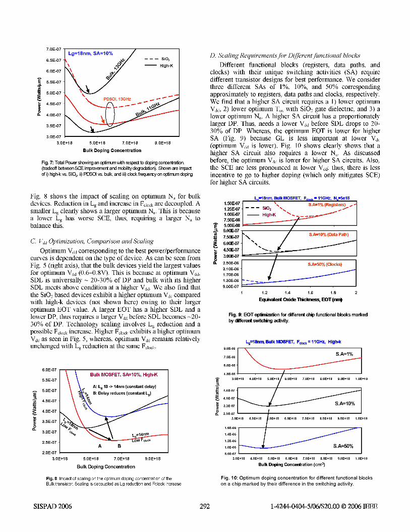
optimum EOT minimizing total power (Fig. 3, Fig. 4). Asdiscussed earlier, the optimum is a consequence of the tradeoffbetween GL and SDL. Fig. 3 shows that the optimum EOTincreases with doping concentration for a given bulk device.This is because of a lower Vt and a resulting higher verticalfield for a higher Na devices. Fig. 3 also clearly depicts a moredramatic relief in power with EOT reduction for lower Naowing to a worse short channel control in lower Na devices.Fig. 4 compares the EOT optimization for different types oftransistors. The presence of the extra Cdiff in the bulk transistorcompared to PDSOI, requires a lower Vt to get the same delay,increasing GL, thus, forcing a larger optimum EOT. Further,the DGFETs have low vertical electric field (hence, GL), thus,can afford a low EOT. In addition to the optimum EOT trend,Fig. 4 also shows the bulk devices exhibiting the most and theDGFETs (already good SCE) the least improvement in thepower with EOT reduction (using high-k). This is because theexistence of the parasitic Cdiff in bulk devices affords anadditional increase in Vt with EOT reduction on top of thatgained because of improvement in SCE. Thus, high-kdielectrics are most advantageous for bulk devices.
Lg=18nnm, BDulk MOSFET, SA=1100%, F<:,o.,k=IIGHz1.00E-06-X1.O-6-Gate Leakag~
E Dominiates
68.OOE-07 e3
IL ~ ~ I46.OOE-07
High-K2.OOE-07 -Sll
1 1.2 1.4 1.6 1.8Equivalent Oxide Thickness, EOT (nm)
Fig. 3: Figure showing existence of optimum EOT and its trendswith different doping concentration for bulk MOSFET
Finally, optimum EOT (for SiO2 gate dielectric) as afunction of technology scaling is studied by decoupling theimpacts of the accompanying delay, and Lg reduction. Adecrease of 3000 in both Lg and delay results in -10%increase in optimum EOT. This is primarily because of ahigher GL at faster speeds due to a lower Vt requirement.
B. Optimized Power/Performance Curves and DopingFig 5 plots the globally optimized power/performance
curves for three devices, Bulk, PDSOI, and DGFET with high-k gate dielectric and Lg of 18nm (45nm node). Both bulk andPDSOI, in turn, have three curves corresponding to differentdoping concentrations. Fig. 6 shows a similar plot for an Lg of14nm, roughly corresponding to 32nm technology node. Inthese figures, the DGFET dissipates the least power followedby PDSOI and bulk, with the discrepancy increasing for higherFc1ock. Within the bulk or PDSOI devices there is an indicationof an optimum with respect to doping. This is explicitly seen inFig. 7, which plots the optimum total power vs. Na at differentFc1ocks. The optimum Na is a result of the tradeoff betweenbetter electrostatics, but worse mobility, subthreshold slope,and CdMf as Na is increased. Fig. 7 also shows that the optimumNa for PDSOI is larger than bulk. This is because an increasein Na results in an extra penalty for bulk compared to PDSOIin the form of an increases in CdM.
o 9.OE-079a0E
O I 7.OE-07
.N r-E.2 5.OE-070.2-
i a 3.OE-070
CD
1.OE-07
8 10 12 14aock Frequency (GHz)
0.80
0.70.6 _
0.5 cn
0.4 %<
0.3 °-0.2 (
0.1 0
016
Fig. 5: The globally optimized power vs. clock frequency curves (left axis) for competingdevices (Bulk, PDSOI and DGFET) with high-k at 45nm HP node. The dots show
corresponding optimum Vdd (only 5e18 cm3 doping is plotted for bulk/PDSOI) on right axis.
DGFET Vdd * Bulk Vdd PDSa Vdd
5.OOE-07
E 4.OOE-07
0--- 3.OOE-07CD
0I3-X~ 2.OOE0E7-W
1.OOE-071 1.2 1.4 1.6 1.8
Eciuivalent Oxide Thickness EOT (nm)Fig. 4: Variation in optimum EOT as a function of different devices. Arrows pointto optium EOT for the SiO2 gate dielectric. High-K advantage is largest of bulk.
9 10 11 12 13 14
- 1
-0.9
-0.8
-0.7
-0.6
-0.5
-0.4
-0.3
-0.2
-0.1
0O
0
cnBr_
Q
1-1
15 16 17
Clock Frequency (GHz)
Fig. 6: The globally optimized power vs. dock frequency curves (left axis) similarto Fig. 5 but for the mor aggressive 32nm high performance node.
1-4244-0404-5/06/$20.00 © 2006 IEEESISPAD 2006 291
7.0OE-07-
6.5 E-07 - -- Si02
6.OE-07 --ig-
E5.5E-07-
5.OE-07-
4.5E-07
0.4.OE-07 K
3.5 E-07
3.0OE-073.OE+18 5.OE+18 7.OE+18 9.OE+18
Bulk Doping Concentration
Fig. 7: Total Paotershowing an optimum 'Mth respect to dopimg concentration.(tradeoff betAeen SCE improvement and mobility degradation). Showvn are impactofi) high-k vs. SIO2, ii) PDSOI vs. bulk, and iii) clack frequency on optimum doping
Fig. 8 shows the impact of scaling on optimum Na for bulkdevices. Reduction in Lg and increase in F,10,k are decoupled. Asmaller Lg clearly shows a larger optimum Na. This is becausea lower L g has worse SCE, thus, requiring a larger Na tobalance this.
C. Vdd Optimization, Comparison and ScalingOPtiMUM Vdd corresponding to the best power/performance
curves is dependent on the type of device. As can be seen fromFig. 5 (right axis), that the bulk devices yield the largest valuesfor optiMUM Vdd (0.6-0.8V). This is because at optiMUM Vdd,SDL is universally -20-30o of DP and bulk with its higherSDL meets above condition at a higher Vdd. We also find thatthe SiO2 based devices exhibit a higher optiMUM Vdd comparedwith high-k devices (not shown here) owing to their largeroptimum BOT value. A larger BOT has a higher SDL and alower DP, thus requires a larger Vdd before SDL becomes -20-300o of DP. Technology scaling involves Lg reduction and apossible F,10,k increase. Higher F,10,k exhibits a higher optimumVdd as seen in Fig. 5, whereas, optiMUM Vdd remains relativelyunchanged with Lg reduction at the same Fc1ock.
0
a-
6.OE-07-
5.5E-07-
5.OE-07-
4.5E-07-
4.OE-07-
3.5E-07-
3.OE-07-
2.5E-07-
20OE-07 -3.OE+1 8 5.OE+l18 7.OE+18 9.OE+18
Bulk Doping Concentration
Fig. 8: Impact of scaling on the optimum doping concentration of theBulk transistor. Scaling is decoupled as Lg reduction and Fdock increase
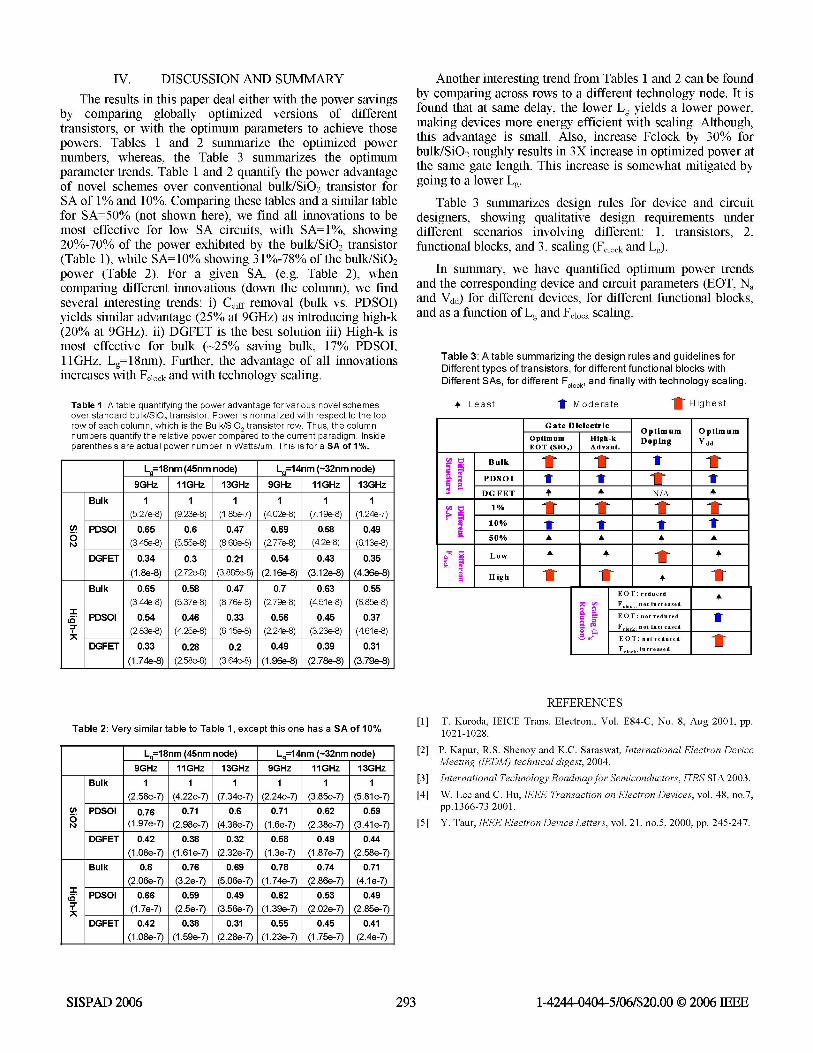
D. Scaling Requirements for Differentfunctional blocksDifferent functional blocks (registers, data paths, and
clocks) with their unique switching activities (SA) requiredifferent transistor designs for best performance. We considerthree different SAs of tOo, 1000, and 500o correspondingapproximately to registers, data paths and clocks, respectively.We find that a higher SA circuit requires a 1) lower optimumVdd, 2) lower optimum Tox with SiO2 gate dielectric, and 3) alower optimum Na. A higher SA circuit has a proportionatelylarger DP. Thus, needs a lower Vdd before SDL drops to 20-3000 of DP. Whereas, the optimum BOT is lower for higherSA (Fig. 9) because GL is less important at lower Vdd(optiMUM Vdd iS lower). Fig. 10 shows clearly shows that ahigher SA circuit also requires a lower Na. As discussedbefore, the optiMUM Vdd iS lower for higher SA circuits. Also,the SCE are less pronounced at lower Vdd; thus, there is lessincentive to go to higher doping (which only mitigates SCE)for higher SA circuits.
E)
0~
1 1.2 1.4 1.6 1.8
Eqiiviet Oxidde Thickness, EOT(mn)2
Fig. 9: EOT optimization for different chip functional blocks markedby different switching activity.
9.OE 08-
7.5E 08-
6.OE 08-
S.A=l%
I~~~~~~~~~~~~~~~~~~~~~~~~~~~~~~~~~~~~~~~~~4.5E 083.OE+18 4.0OE+18 5.OE+1 6.0E+18 7.OE+18 8.0E+18 9.OE+18 1.OE+19
4.8E 07
4.OE 07
3.3E 07SA= %
0IL 2.5E 07
3.OE+18 4.0E+18 .OE+18 6.OE+18 7.0E+18 8.OE+18 9.OE+18 1.OE+19
1 .6E-06
1A.E-06
1 .2E-06
1 .OE-06 S.A=50%8.OE-07
3.OE+18 4.OE+18 5.OE+18 6.OE+18 7.OE+18 8.OE+18 9.0OE+18 1.OE+19
Bulk Doping Concentration (cmw3)
Fig. 1 0: Optimum doping concentration for different functional blockson a chip marked by their difference in the switching activity.
SISPAD 2006 292 ~~~~~~~~~~~~1-4244-0404-5106/$20.00 02006 IEEESISPAD 2006 292
IV. DISCUSSION AND SUMMARYThe results in this paper deal either with the power savings
by comparing globally optimized versions of differenttransistors, or with the optimum parameters to achieve thosepowers. Tables 1 and 2 summarize the optimized powernumbers, whereas, the Table 3 summarizes the optimumparameter trends. Table 1 and 2 quantify the power advantageof novel schemes over conventional bulk/SiO2 transistor forSA of 1% and 10%. Comparing these tables and a similar tablefor SA=50% (not shown here), we find all innovations to bemost effective for low SA circuits, with SA= t%, showing20%-70% of the power exhibited by the bulk/SiO2 transistor(Table 1), while SA=10% showing 31%-78% of the bulk/SiO2power (Table 2). For a given SA, (e.g. Table 2), whencomparing different innovations (down the column), we findseveral interesting trends: i) Cdiff removal (bulk vs. PDSOI)yields similar advantage (25% at 9GHz) as introducing high-k(20% at 9GHz). ii) DGFET is the best solution iii) High-k ismost effective for bulk (-25% saving bulk, 17% PDSOI,11GHz, Lg 18nm). Further, the advantage of all innovationsincreases with F,l10k and with technology scaling.
Table 1: A table quantifying the power advantage for various novel schemesover standard bulk/SiO2 transistor. Power is normalized with respect to the toprow of each column, which is the Bulk/SiO2 transistor row. Thus, the columnnumbers quantify the relative power compared to the current paradigm. Insideparenthesis are actual power number in Watts/[im. This is for a SA of 1%.
Lg=18nm (45nm node) Lg=14nm (-32nm node)9GHz 11GHz 13GHz 9GHz 11GHz 13GHz
Bulk 1 1 1 1 1 1(5.27e-8) (9.23e-8) (1 .85e-7) (4.02e-8) (7.1 9e-8) (1 .24e-7)
L' PDSOI 0.65 0.6 0.47 0.69 0.58 0.490 (3.45e-8) (5.55e-8) (8.66e-8) (2.77e-8) (4.2e-8) (6.13e-8)
DGFET 0.34 0.3 0.21 0.54 0.43 0.35(1 .8e-8) (2.72e-8) (3.885e-8) (2.1 6e-8) (3.1 2e-8) (4.36e-8)
Bulk 0.65 0.58 0.47 0.7 0.63 0.55(3.44e-8) (5.37e-8) (8.76e-8) (2.79e-8) (4.51e-8) (6.85e-8)
I PDSOI 0.54 0.46 0.33 0.56 0.45 0.37(2.83e-8) (4.25e-8) (6.15e-8) (2.24e-8) (3.23e-8) (4.61e-8)
DGFET 0.33 0.28 0.2 0.49 0.39 0.31(1 74e-8) (2.58e-8) (3.64e-8) (1 .96e-8) (2.78e-8) (3.79e-8)
Table 2: Very similar table to Table 1, except this one has a SA of 10%
Lg=18nm (45nm node) Lg=14nm (-32nm node)9GHz 11GHz 13GHz 9GHz 11GHz 13GHz
Bulk 1 1 1 1 1 1(2.58e-7) (4.22e-7) (7.34e-7) (2.24e-7) (3.85e-7) (5.81e-7)
cn PDSOI 0.76 0.71 0.6 0.71 0.62 0.59o (1.97e-7) (2.98e-7) (4.38e-7) (1.6e-7) (2.38e-7) (3.41e-7)
DGFET 0.42 0.38 0.32 0.58 0.49 0.44(1 .08e-7) (1.61 e-7) (2.32e-7) (1 .3e-7) (1 .87e-7) (2.58e-7)
Bulk 0.8 0.76 0.69 0.78 0.74 0.71(2.06e-7) (3.2e-7) (5.06e-7) (1.74e-7) (2.86e-7) (4.1e-7)
I PDSOI 0.66 0.59 0.49 0.62 0.53 0.49(1 .7e-7) (2.5e-7) (3.56e-7) (1 .39e-7) (2.02e-7) (2.85e-7)
DGFET 0.42 0.38 0.31 0.55 0.45 0.41(1.08e-7) (1 .59e-7) (2.28e-7) (1.23e-7) (1 .75e-7) (2.4e-7)
Another interesting trend from Tables 1 and 2 can be foundby comparing across rows to a different technology node. It isfound that at same delay, the lower Lg yields a lower power,making devices more energy efficient with scaling. Although,this advantage is small. Also, increase Fclock by 3000 forbulk/SiO2 roughly results in 3X increase in optimized power atthe same gate length. This increase is somewhat mitigated bygoing to a lower Lg.
Table 3 summarizes design rules for device and circuitdesigners, showing qualitative design requirements underdifferent scenarios involving different: 1. transistors, 2.functional blocks, and 3. scaling (F,l10k and Lg).
In summary, we have quantified optimum power trendsand the corresponding device and circuit parameters (EOT, Naand Vdd) for different devices, for different functional blocks,and as a function of Lg and Fclock scaling.
Table 3: A table summarizing the design rules and guidelines forDifferent types of transistors, for different functional blocks withDifferent SAs, for different FCloCk, and finally with technology scaling.
+ Least t Moderate lW H ighest
I
REFERENCES[1] T. Kuroda, IEICE Trans. Electron., Vol. E84-C, No. 8, Aug 2001, pp.
1021-1028.[2] P. Kapur, R.S. Shenoy and K.C. Saraswat, International Electron Device
Meeting (IEDM) technical digest, 2004.[3] International Technology Roadmapfor Semiconductors, ITRS SIA 2003.
[4] W. Lee and C. Hu, IEEE Transaction on Electron Devices, vol. 48, no.7,pp.1366-73 2001.
[5] Y. Taur, IEEE Electron Device Letters, vol. 21, no.5, 2000, pp. 245-247.
1-4244-0404-5/06/$20.00 © 2006 IEEESISPAD 2006 293