practical implementation of a general computer...
TRANSCRIPT

190 IEEE JOURNAL OF SOLID-STATE CIRCUITS, VOL. SC-15, NO. 2, APRIL 1980
Practical Implementation of a General ComputerAided Design Technique for Switched
Capacitor Circuits
HUGO J. DE MAN, JAN RABAEY, GUIDO ARNOUT, AND JOOS VANDEWALLE, MEMBER, lEEE
Abstract–In this paper a general and efficient CAD method for simu-lation of switched capacitor filters and A/D and D/A converters, isdemonstrated. It is based on the direct implementation of controlledswitch branches into the widely used modified nodal analysis techniqueand is therefore in contrast to other methods, directly compatible withexisting CAD techniques. It allows for dc, time domain, and frequencyresponse calculations for arbitrary clock cycles and aU types of inputs(piecewise constant, sample and hold, and continuous). The circuit canalso contain resistors and allows for nordiiear time domain analysis too.
As implemented in the DIANA program it allows for fult top-downdesign from principle to transistor level, including clock drivers, controllogjc, etc. Input is directly from the circuit diagram. The method isillustrated by practical design examples.
I. INTRODUCTION
IN the last few years, switched capacitor circuits have been
successfully used for the design of single chip metal-oxide-
semiconductor-large-scale integration (MOS-LSI) filters and
A/D and D/A convertors [1] -[4]. This technique has caused abreakthrough of analog LSI signal processing. Research foradequate CAD tools for such circuits is motivated by the pres-ent lack of adequate design procedures and a large number ofparasitic effects such as clock-feedthrough, offset, drift, straycapacitance, nonlinearities, aliasing, and noise problems.
These systems are indeed hard to simulate by existing CADprograms due to the very large ratio between sample and signalfrequency which leads to excessive central processing unit
(CPU) time for time domain analysis.Another problem is that these circuits are basically time-
variant circuits and although in the past [5] , [6] and recently[7] -[9] analysis techniques for switched networks have beendescribed, none of these methods are directly compatible withtoday’s CAD programs and/or are restricted to a given class ofclock sequences (e.g., two-phase clocks). They require thesetup of a number of different matrices for the different clockphases [7] , [9] , are difficult to generate from the network de-scription, and do not allow for switched capacitor networkscontaining resistive dividers. Furthermore, they do not allow
Manuscript received June 27, 1979; revised November 2, 1979. J.Rabaey and G. Arnout are supported by the Belgian I.W.O.N.L.
The authors are with the Department E1ektrotechniek-E. S.A.T.,Katholieke Universiteit Leuven, Heverlee, Belgium.
for the study of clock-feedthrough, nonlinear, and parasiticeffects.
In this paper a general method overcoming all the above re-strictions is presented. Crucial to the method is the introduc-tion in Section II of controlled switch branches into a single
modified nodal admittance (NINA) matrix. These branchesranging from ideal switched to full MOS models can be intro-
duced in any circuit simulator based on MNA (e.g., SPICE2
[15], ASTAP [16], DIANA [12], [17]). It will be shownthat there is no restriction on the clocking sequence. Classicaldetailed resistive response using numerical integration is pos-sible as well as a 1 calculation/clock phase analysis using chargeconservation. It is shown that the latter case can be intro-duced with only minor modification in existing CAD programs.Nonlinear as well as resistive voltage division effects, can also
be included (Section III).
Implemented in mixed-mode simulator DIANA [12] , mixed
analog digital circuits can be analyzed as demonstrated in Sec-
tion III, case B. In Section IV a general method for frequency
analysis using arbitrary ifiputs is demonstrated based on a sim-ple example, and applications to practical circuits are given. Incontrast to, e.g., the DINAP-prograrn [19] , the input descrip-tion to DIANA follows immediately from topology, and nomodeling or transposition of the circuit into a digital filterstructure is needed. Also continuous inputs can be handled in
the frequency domain, while programs as DINAP are essentiallylimited to piecewise constant inputs.
The implementation of the method in DIANA leads to afully operational top-down design tool for mixed analog-digital MOS-LSI circuits.
11. IMPLEMENTATION OF SWITCHED CAPACITOR
NETWORKS IN EXISTING CAD PROGRAMS
Crucial to the simulation method to be presented is the in-
troduction of a hierarchical set of switch branches into the
MNA-formalism, which is used in most existing CAD programs
[13] .
This method allows for a simple topological description of
the network and is extremely simple to implement. We will
start by looking at switched capacitor networks ~ Sc con-
sisting (for the time being) of ideal switches ($, capacitors
(C), and dependent (A) and independent (E) voltage sources.
This is no direct restriction since all practical switch capacitor
0018-9200/80/0400-0190 $00.75 @ 1980 IEEE

DE MAN et al.: GENERAL COMPUTERAIDED DESIGN TECHNIQUE 191
networks are based on a sequence of equilibrium states. The
design of detailed circuitry to satisfy the speed requirements
can be done in a “top-down” fashion by simulating criticalparts at a more detailed transistor level (see Section III, case B).
Consider now a node i of a R SC network to which all theabove elements are connected (Fig. 1). An ideal switch S iscontrolled by a Boolean clock variable OS e {O, 1}. @S= O and
% = 1 correspond to an open, respectively closed, switch. LetVi(k) be the voltage at node i at the end of the time intervalA(k) and let qj‘k) be the charge transferred in branch j duringthe time interval A(k). The clock states (Fig. 1) define a timesequence T={to, tl . . . tk.~,tk...}and timeslotsA(l)0..
A(k) etc. We fu~ther assume that the independent voltagesour’ces E(t)only change value at the switching instants tk e ~and call them piecewise constant [7] , i.e., 13(t G [tk. ~, tk] ) =
E(k). This restriction will be removed later [see (5)]. Under
the above conditions, and similar to the MNA method [13],currently used in most CAD programs, an independent set ofequations for a transition from A(k” 1) to A(k) consists Of
1) charge conservation inn independent nodes, e.g., in nodei (Fig. 1):
=Cu(k- 1) _ ~uy -i
with
Jqj(k) = ‘kij(t) dt.
tk.1
Equation (1) can also be
1)(1)
(2)
obtained by integrating KCL at node
i over the slot A(k). This equation gives rise to row i in theMNA representation of Fig. l(a) in Fig. l(b);
2) branch relations for all E, A, and S. Tb.e branch relationsfor E and A are trivial from Fig. l(b). Impc~rtant is the imple-mentation of switch branch S as follows:
$#tlp –(k) (k) = o,- flf?rp+-@sqs (3)
j$s denotes the Boolean complement of OS.From (1) and (3) it is clear how S is implemented into the
matrix !i ‘k). As shown by the dotted lines in Fig. 1(b) every
element of %Sc has a simple entry (stamp) into the matrix
’11‘k) which is nothing but the widely used MNA [13] matrixnow also including controlled switches and operating on a vet.tor X(k) of voltages and charges.
Fig. 2 shows a number of voltage controlled switch branches,their implementation in the %1matrix, and their description in
the DIANA program. The upper four branches are for T(SCnetworks. The pass switch is a first-order MOS triode switchmodel for studying clock feedthrough and :switching transienteffects in classical transient analysis (see Section III), In con-trast to previously published methods [7] , [9] these switch
models give a direct link between circuit design and singleMNA matrix. Clearly no restriction is imposed on clock se-
quences which can be derived from, e g., digital circuit parts(see Section III, case B). In closed form the equation in Fig.l(b) can be written as
‘“i“oil t
——
1
i
k
I
m
P
E
A
s
(a)
1 iklmp EAs
c .~ I
c c:_——_
iii——_—_ —_— ——1 -1 1/
.—— —— ——————
1 -1 -A I
—-—— ——————————Jk)
, d’ dl–––––––––– —––––-.
Jk)
(b)
x
x
+k)
Y(k)
=
qE(k)
qA(k)
~~(k)
(k) _~.
(k-1):( Vi-y)
(k-1)>(Vj-Vi)
~(k)
o
S(k,k-1)
L
Fig. 1. (a) Resistorless switched capacitor network and clock defini-tion. @iis a Boolean variable. tk ~~ is the time immediately preced-ing the clock transition for time slot A(k). (b) Matrix obtained fromcharge conservation and switch branches is an MNA matrix,
Equation (4) relates the soluting during A{k) to the one duringA(k - ‘). X(k) can be solved by techniques discussed in [13] .
If the signal sources Uin(k) are continuous instead of piece-wise constant, i.e., Uifl(t)jthen it can easily be shown that (4)
can be written as
t;. ~ is defined as in Fig. l(a). Equations (4) and (5) will be
of use in the Appendix.Returning to Fig. l(b) for piecewise constant inputs notice
that the capacitor stamp is equivalent to the widely used back-ward Euler integration companion model for a capacitor for aunit time step [14] . This then leads to the following generalsimulation procedure for any switched capacitor network witharbitrary clock sequence and easy to implement in MNA based
simulators:1) introduce switch stamp as in Fig. 2;
2) use backward Euler integration with unit time step;3) bypass all time step control. Time points coincide with
clock sequence to,tl“““tk“““;
4) start from inital values U$?))= rr$) - up) for all capac-itors. Default is zero;

192 IEEE JOURNAL OF SOLID-STATECIRCUITS, VOL. SC-15, NO. 2, APRIL 1980
‘K-Tat‘k+l
Stamps DIANA Description
,,s
‘--let--’+-’ :1:”’$1:,1’, .JM
v,
“J . S3XX IJMKL VT=
‘M
%
@w; 1 S2XX I J K L C= VT=
4C v,;
Fig. 2. Time controlledswitch is a first-ordereffects.
“=–= a“; . K5”M-. “,-
pass switch SXXX IJGE R=
O=. (”...,. [V,.v, )-v,] VT= ‘W= ‘OX= PASS
c . 8/2C.x a
switch models used in DIANA. The passMOS triode model including channel charge
5) generate (4) from topology description and solve for-y(k) ;
6) interpret all i(k) G X(k) as q(k).This method has been implemented in the DIANA program
as an OPTION. A careful look at Fig. 1(b) also reveals that the
method is fully compatible with the normal transient mode of
simulation if backward Euler integration with A # 1 is used
and all q are taken as currents i.Therefore in DIANA all modes of simulation from pure de-
tailed transistor transient up to the above R Sc simulation arepossible. Since DIANA also allows for mixed analog, timing,and logic simulation a full mixed analog-digital MOS-LSIcircuit can be simulated as demonstrated in the followingexamples.
III. LINEAR AND NONLINEAR TIME RESPONSECALCULATIONS–CASE STUDIES
CaseA: Study of Offset Drift in a Switched CNetwork
Fig. 3(a) shows a possible method to avoid large capacitorratios if a large pole-zero to sampling frequency is required.
Within the basic clock cycle (K.., I& ~) a charge redistri-bution using clocks (V& ~, ~n ~) takes place on (Cl, C;) and(C,, C’$ comparable in magnitude to CI and Co. We want tostudy the influence of op amp offset, EOFS = 50 mV.
Fig. 3(b) shows the DIANA output plot of a classical tran-sient analysis over 25 clock periods using PASS switch models.
A 40 points/basic clock cycle has been used (1000 time steps).Fig. 3(c) shows the result of the new MNA method over 650
(a)
o 1,ma 250ps
b(volt)
-0. s1 r
(b)
.465L(c)
Fig. 3. Example of the simulation of offset caused drift. (a) Filter us-ing charge redistribution in a mbclock cycle. CI = 6 pF, C2 = 6 pF,Ci = 6.66 PF, C;= 16.6 PF, Cl = Co = 20 PF, EOFS= 50 mV. (b)Classical transient analysis result using pass switches for 25 clockcycles– 1000 time points computed. (c) Result of new simulationmethod over 650 clock periods requiring the same computer time as(b) (30 S IBM 370/158).
clock periods, calculating 1 solution/time slot. The simulationreveals -4.65 V drift due to 50 mV offset of the op amp. This
result was discovered by CAD and is caused by inadequate
feedback of output offset errors by redistribution on (C2, C;).Notice that the new method is ca. 26 times faster than classicaltransient analysis as both run times are the same (20 s CPU onIBM 370-1 58). If a nonlinear MOS model had been used, thedifference would be about 100 “ “ .150. Notice also that noproblem occurs due to the complex clock sequence. The fol-lowing example shows an application of fully mixed analog-digital simulation using pass switches.
Case 1): Detailed Arralysr’s of a D&tally Controlled Filter
Fig. 4(a) shows a pole-zero filter with a capacitor bankc,””” C4 which can be digitally controlled by the user by anup-down command to accentuate or decrease frequencies inexcess of 2.5 kHz (audio treble control filter). Fig. 4(b) showsthe result of a hybrid transient analysis of the mixed analog-digital circuit using 1800 time steps of 1 ps, using pass-switchmodels and 1 pole op amp models (unity gain bandwidth:1 MHz).
The input signal is a 10 kHz sine wave with an amplitude of0.1 v.
Notice the clock-feedthrough effects on sample and hold, andthe charge dumping spikes in op amp input. Spike A results
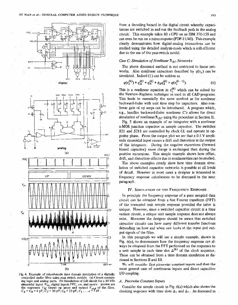
DE MAN et al.: GENERAL COMPUTER AIDED DESIGN TECHNIQUE 193
F
VvllV;C2 VM’C3VM’L& ‘H
“MCI VMC2 v~C3 vMcL nCl
,, ,, 1
(a)VOLT
FFC
I II I 1 1~=
5
0
7
5
UP DOWNo
q“ 01
0
0.01‘M
o
VOUT0.3
0
I,,, ,. .—
0% TIME lrflo p=’
(b)
Fig. 4. Example of mixed-mode time domain simulation of a digitallycontrolled audio fiiter using pass switch models. (a) Circuit contain-ing logic and analog parts. (hl Simulation of full circuit for a 10 kHzsinusoidal input Vin, digital inputs FFC, UP, and. DOWN. Shown arethe responses VM (input op amp) and output Vout of the filter.CA= CB=4PF, CT=30PF; CO=lOPF, C1 . ..4= 5PF.
from a decoding hazard in the digital circuit whereby capaci-
tances are switched in and out the feedback path in the analog
circuit. This example takes 80 s CPU on an IBM 370-158 andcan even be run on amimcomputer(PDP-11 /40). This example
clearly demonstrates how digital-analog interactions can be
studied using the detailed analysis-mode which is still efficientdue to the use of the pass-switch model.
Case C: Simulation of Nonlinear fist Networks
The above discussed method is not restricted to linear net-works, Also nonlinear capacitors described by q(uC) can besimulated. Indeed (1) can be written as
(k) = q(uc ).q(uy)) + qf) + qg) + Osqs(k- 1) (6)
This is a nonlinear equation in v~) which can be solved bythe Newton-Raphson technique as used in all CAD programs.This leads to essentially the same method as for nonlinearbackward-Euler with unit time step for capacitors. Also non-linear gain of op amps can be introduced. A program which,
e.g., handles backward-Euler nonlinear C’s allows for direct
simulation of nonlinear E Sc using the procedure in Section II.
Fig. 5 shows an example of an integrator with a nonlinear
n-MOS junction capacitor as sample capacitor. The switches
S21 and S211 are controlled by clock CL and operate in op-posite phase, From the output plot we see that a O.5 V ampli-tude sinusoidal input causes a drift and distortion in the outputof the integrator. During the negative excursions (forwardbiased capacitor) more charge is exchanged than during thepositive excursions. This simple example shows how offset,drift, and distortion effects due to nonlinearities can be studied.
The above examples clearly show how time domain simu-
lation of switched capacitor networks is possible at all levels
of detail. However in most cases a designer is interested infrequency response calculations to be discussed in the next
paragraph.
IV. SIMULATION OF THE FREQUENCY RESPONSE
In principle the frequency response of a pure sampled data
circuit can be obtained from a fast Fourier transform (FFT)of the truncated unit sample response provided the latter isunique. However, since a switched capacitor circuit is a time
variant circuit, a unique unit sample response does not always
exist. Moreover the designer should be aware that switched
capacitor circuits can have many different transfer functionsdepending on how and when one looks at the input and out-put signals of the filter.
In this paragraph we will use a simple example, shown inFig. 6(a), to demonstrate how the frequency response can al-
ways be obtained from the FFT performed on the responses toa unit sample in each time slot A(k) of the clock sequence.These can be obtained from a time domain simulation as dis-
ctissed in Sections II and III.We will Gonside. first piecewise constant inputs and then the
most general case of continuous inputs and direct capacitive1/0 coupling.
A. Piecewise Constant Inputs
Consider the simple circuit in Fig. 6(a) which also shows theclocking sequence with time slots A 1 and Ay. As discussed in

194 IEEE JOURNAL OF SOLID-STATE CIRCUITS, VOL. SC-15, NO. 2, APRIL 1980
(a)
VIN
o
-0.5
-1.51
(c)
Fig. 5. Example of nonlinear switched capacitor network simulation.(a) An integrator with nonlinear sampling capacitor. (b) Sinusoidalinput. (c) Simutated output waveform showing distortion and drift.
Section I a piecewise constant input for Uin(t) is defined asUin(t) sampled at the beginning of each time slot and then helduntil the next time slot.
This defines samples ~in(tl - T), Uin(0), Uin(tl ), Uin(t2) . “ “
as shown in Fig. 6(a). It is common practice to consider the
output as sampled only during one particular time slot [7]
within the clock period T. For example in Fig, 6(a) it is na-
tural to consider the output U. as sampled at tl + nT (begin-ning of time slot A2 ). Call this value U.(tz ).
For a piecewise constant input it is designers practice to writethe difference equations of the circuit by inspection usingcharge conservation. This leads for Fig. 6(a) to
1) transition at O:
u~(o) = U)(tl - T); (7)
2) transition at tl:
C(U()(t~) - Zlrj(0)) + C(U()(t~) - Uin(0))
+ 2C(Uo(t~) - Ui~(t~)) = O. (8)
From (7) and (8)
Vo(tl) - ~ rJo(tI - T’)= $ uin(~l) + $ uin(0)- (9)
Let u now be the pulsation of a sinusoidal input phasorYin(jti) of which the piecewise constant version is applied to
the circuit and let U$)(jU) be the phasor corresponding to thissame pulsation in the output r$)(t) = rro(t2 ) sampled during
o
-20
~.y $’+2
(a)
r --
0 AMP (db)
1
2
3
-20 _P2= 1/2 10gf=
(b)
f5/2
AMP (db)
r15
P;ecew;se constant I npufs [og /=.
(c) fs/2
Fig. 6. Illustrative example showing different simulation modes. (a)Example circuit, its clocking sequence and piecewise constant input.(b) Simulated frequency response for duty cycle p2 = 0.5 and out-put sampled at fl and held over 2“. Curve 1: for continuous input,Curve 2: for piecewise constant input, and Curve 3: for input sam-pled and held over period 1“. (c) For piecewise constant input anddifferent p2.
time slot A2. 1 Then we can define the transfer function for
the output sampled during AZ as follows:
iYz (jti) = V$)(j@)/Vin(j@). (lo)
Using this practical definition and Fourier transform techniques
one obtains
1/2 l/4e-jwpl T
H2 (@)=1- l/4e-jG+ 1- l/4e-ju T
(11)
wnn 01 = Al/T as defined in Fig. 6(a).We will now show how this transfer function can be ob-
tained by the calculation of unit sample responses using thesimulation method discussed in Sections II and III.
Indeed when driving the circuit with a unit sample input, re-spectively, on time slot A ~ and A2 the time domain simulationgives the time series shown in Table I which can easily be veri-fied by inspection of Fig. 6(a).
Table I clearly shows that two distinct unit sample responses
1only the baseband spectrum is considered here.

DE MAN et al.: GENERAL COMPUTER AIDED DESIGN TECHNIQUE 195
TABLE IUNIT SAMPLE RESPONSESFOR FIG. 6(a). & AND & ARE UNIT SAMPLES,
RESPECTIVELY,DURING AI AND Al. hi(t) AND h4t) ARE THE SAMPLE
RESPONSES. [UNDERLINEDARE THE OUTPUTS SAMPLEDAT TIME fI
(TIME SLOT A,).
Al AZ Al AZ Al AZ
tl+T
4---4-4t2+T t, i- 2T tz + 2T
II I I
1 0 0 0 0 0 0
0 1/4 1/4 1/16 1/16 1/64 1/64 ..-
0 1 0 0 0 0 0
0 1/2 1/2 1/8 1/8 l@ 1/32 . . .
TABLE 11UNIT SAMPLE RESPONSESAT AZRESULTING FROM UNIT SAMPLEAT
A, AND Az, RESPECTIVELY,AND THEIR FOURIERTRANSFORMS
1hz,l(r) 1/4 1/16 1/64 , . s H2,1(ejwT) = ~ (12)
1 -;e-iwT
1hz,z(t) 1/2 1/8 1/32 ~ H2, Je@T) = ~ (13)
1 -+NJT
sampled at tl + nT exist. We call them h:,,l (t) and izz,z (t).
They are represented in Table II together with their Fouriertransforms Hz,l (e~w~) and H;,z (e~”~) as c}btained from the
z transforms by using z-l = e-J W’.
Inspection of(11) and (12), (13) shows that
HQ(ju) = lY2,z(e@T) + e-~wtl Hz,l (e@~”). (14)
This is a natural result, since IZz,l (t) results from an input sig-nal sampled at the beginning of the previou~j~~le slot, i,e, atime t1 earlier. This causes the phase factor e in (14).
Notice now that Hz,l (e@ T), H,,a(e@t) as well as H, (.ko)can easily be obtained by applying an FFT algorithm to fiz,l (t)and hz,2 (t) resulting from a time domain simulation of the
unit responses using the method of Sections, II and III. If theoutput is sampled and held during period T (as is the case
here) one has to multiply the FFT result (14) by
f= ~-jw T/z sin (uT/2)u T[2 -
(15)
The result of a DIANA simulation of Fig. 6(a) for piecewiseconstant input, PZ = O.5, and the output sampled at tl andheld over T are shown in Fig. 6(b), curve 2, whereas Fig. 6(c)
shows a simulation for three different values of the duty cyclePz. Clearly the duty cycle has a big influence on this circuitdue to the phase effects it causes in the transfer function. Thetechnique demonstrated here for a simple example can be gen-eralized for all switched capacitor networks dkiven by piecewisecontinuous inputs as follows.
Consider the switched capacitor networks ?l, [see Fig. 7(a)]
with clock signals @l “ “ “@n defining 1 time slots Ai in eachperiod T. The unit sample input on time slot i causes a time
series on the output of fi~ [see Fig. 7(b)] .Observing the output only on time slot k of each period, a
time series is generated [see Fig. 7(b)] of which the Fourier
transform is ~Q(ejwT). This is the transfer function, similarto (10), from a sinusoidal input sampled in time slot i to theoutput, sampled in time slot k, and of which the phasor at thesame frequency w of the input is considered. This can bedone in the same way for all time-slots i (i= 1,2) which leads
tOHk,l ,fik,2 “ “ “Hk,l.
For the baseband frequencies u then the total transfer func-tion for time slot k, defined as Hk(jco), can be obtained by
superposition of the ~k ~ for i = 1 0 “ .1 each multiplied withthe phasefactor e
-~LIJ(~k’_1- ti-1)since they result from the
sinusoidal input considered a time tk_~- ti_1 earlier or
Hk(jo) = ~ Hk,i(ejWT) “e‘jL’J(tk_ ~ – ti. ~)
(16)k=l
If sampled and held over period T, (16) still has to be multi-plied by (1 5). Notice: 1) (16) is strictly only valid for the base-
band (i.e., 0< u < 27i/T). A rigorous proof of (16), includ-ing full spectrum analysis, is beyond the scope of this paperand is the subject of a separate publication [11] ; 2) (16) indi.cates that often different transfer functions are obtained de-pendent on the output sampling time slot.
The above described algorithm is built into the postprocessorof the DIANA program. It consists of the calculation of the

196
Genera/ Conf/gurat/On
IIN(0”,1i 1 ‘>’ 1! k 1;1+1 21+1
h-( ,b
T
IEEE JOURNAL OF SOLID-STATE CIRCUITS, VOL. SC-I 5, NO. 2, APRIL 1980
/ (c)
Fig. 7. Unit sample response of l-phase switched capacitor filter: (a)general network; (b) response to unit sample input in time slot i; (c);esponse, observed at time slot k. The dashed ifies show the sampleand hold effects.
frequency transforms of the unit sample responses at all time
Slots k= l”” “1 followed by a FFT and the combination ofthese transforms, as described by (16), It also handles the
sin (x)/x effects, caused by the sample and hold effects [see
dashed lines it-rFig. 7(b) and (c)] either over a full or a partialperiod. Let us now look at two cases very often encountered inpractice which are special cases of the discussed method and il-lustrate them by examples.
1) Filters with Input Sampled only During One Time Slot:A large number of switched capacitor filters published latelyhave the property that the input is only sampled during oneparticular time slot, say A 1. In this case all unit sample re-sponses except one are zero and thus according to (16) onlyone unit sample simulation for Al is needed. Consider for ex-
~Ple the cage of the fourth-order Rutterworth filter de~cribedby Jacobs et al. in [3] and shown in Fig. 8(a) together withthe input code for simulations using the DIANA program inFig. 8(b) (left).
It takes only 25 statements to describe the circuits topologyand run control. Notice that 300 points of the unit sample re-sponse are requested with time step DELTA = 1 as discussed inSection II.
The switch models used here are capacitive double throwswitches as described by the S3 model in Fig. 2. They are con-
trolled by clock IP-TPUTCL. As stated in [3] , the frequency re-
sponse depends strongly on the clocking phase: when clockedas in Fig. 8(a) the principle of the lossless digital integrator(LDI) is used. Inverting the clocks of switches S32A, S32B,
I-_3’”(a)
INPuT DIANA
LDI DTI
Ca 5 4 a,d72c; 9 w 11.76C7 1? !3 11.76C9 1? !8 4.872$VA5,?!JUI(xv’? 1,1 7 d q ,K
0 2 CYC
93t A,C! I 9 CL a c=? vT. iS31d Cl id 4 CL 0 C*2 VT.1332A Co 5 0 CL a C*Z VT=lS3?9 Ca IU 9 CL fl C,2 VT,l533A C6 1’3 j CL ? CS2 VTSISI18 C6 ,8 IX CL d Ca~ VT,,
93’44 C! 1!4 S CL ‘7 C.? Vl=lS348 C4 18 17 CL n C*? VT, ISJf $1 j U CL 3 c31 vTzl
(b)
Fig. 8. (a) Fourth-order Butterworth fiiter and (b) DIANA input de-scription for LDI and DTI.
S34A, and S34B gives a direct transfer integrator (DTI) withlarger delay. The underlined statements in Fig. 8(a) showthe input changes in order to modify the phase of the aboveswitches. Fig. 9(a) shows the unique unit-sample response
computed by DIANA for the LDI (curve 1) and the DTI (curve2) case. Fig. 9(b) shows the frequency response obtained froma FFT on Fig. 9(a) for both I.,DI and DTI.
These results agree fully with the measurements presented in
[3] . This simulation takes 18 s CPU time on an IBM 370/158which clearly shows the efficiency of the simulation method,The same example can easily be run on a minicomputer suchas the PDP 11/40.
2) Filters Driven From a Sample and Hold Input: Some fil-
ters are driven from an input which is sampled in time slot i
[time ti - ,, see Fig. 7(b)] and held over clock period T. Theoutput is sampled, say, in time slot k (time tk. 1),
It is easy to see that in this case (16) has to be modified into
(17)
The phase factor exp (-jti(tk _ ~ - ti.~)) results from delaybetween input and output samples whereas the terms in brac-
kets account for responses due to the previous input sample, re-spectively, the actual input sample.
Notice from (17) that also in this case the response can beobtained from the FFT of the unit sample responses hk, j of
the circuit.

DE MANet al.: GENERAL COMPUTER AIDED DESIGN TECHNIQUE 197
0.4v .?----
~d1 LDI
1 -. 2 DTI
.- .. T-...- ----
-O.10.4.-
300
-2
-18
(a)
AMP (db) log F. . . . . . .
>..
‘.2
1 “.
180”PHASE
F-
-0,01 0.02 O.cL 0.1
(b)
Fig. 9. (a) Imprdse response for the circuit in Fig. 8(a) for LDI and DTIclocking. (b) Amplitude and phase responses resulting from FFT onFig. 9(a). Notice that F is the frequency norrrralized to the samplefrequency f~, i.e., F = f/f~
Simulating the circuit in Fig. 6(a) while sampling input andoutput during A2 and holding both constant over period T re-
sults in curve 3 in Fig. 6(b). This result can easily be verified
starting from difference equations. Fig, 6 clearly demonstrateshow careful one has to be in defining the t ransfer function of
switched capacitor networks and indicates the usefulness of asimulation technique in this field.
B. Continuous Inputs
The above described method will not be correct, when the
applied input is continuous, The difference will be especiallyimportant, when a continuous capacitive (or resistive) pathexists between input and output. The importance of this ef-fect, mainly a suppression of the effects of the sample and
holds, which generate additional sin (uT/2)/(d7’/2) compo-nents in the frequency domain, has been demonstrated by Y.P. Tsividis [1O] . The greatest difficulty, prohibiting normalsimulation of the frequency response of circuits with a con-tinuous 1/0 path, is caused by the fact that the output is amixture of discrete and analog signals.
A technique will be demonstrated now, making it possible tosimulate switched capacitor systems with continuous inputsand continuous 1/0 paths still using the unit sample responseshk, i(t) defined in Section IV-A.
Let us again use the example of Fig. 6(a) to illustrate the
technique of which a rigorous proof is given. in the Appendix.Suppose Un(t) is a continuous sinusoidal input of amplitude
1. Due to the continuous couplirig during.& by capacitor 2C,the output is a mixture of sampled and continuous signals as is
clear from Fig. 10(d) which shows a time domain simulationof the output using the DIANA program. As given, in general,
in the Appendix the output can be considered as the super-position of three components shown for this particular case in
Fig. 10(a)-(c) and which are:
1) the continuous input in each time slot A(k) weighted by
the “gain” defined by the instantaneous capacitive feedthroughthrough the capacitive 1/0 path in A(k) [in this case zero dur-ing A ~ and ~ during A2, see Fig. 10(a)] . A different gain mayexist for every time slot;
2) the inverted backward folded sample and hold version of
the signal 1) as shown in Fig. 10(b). The result of adding 1)
and 2) is the shaded area in Fig. 10(a);
3) in each time slot the sample and hold version of the out-
put, due to a piecewise constant input, sampled at the end of
the time slot [see Fig. 10(c)].Notice now the following:
a) terms 1) and 2) disappear when no continuous 1/0 cou-pling is present such as in Fig. 8(a);
b) the frequency response in the baseband can still be ob-tained by using the FFT terms Hk,i(e @T) obtained from the
unit sample responses hfi, ~(t) as discussed in Section IV-A.This is illustrated in Table III.
Indeed the baseband frequency component for time slot
A(k) in 1) is nothing eke than the firSt 5ampze of hk, k(t) orhk,~(()) weighted by duty cycle Pk since h~,k(()) represents theinstantaneous feedthrough from input to output in A(k).
Term 2) for A(k) is the same as 1), but including sin (x)/x ef-fects for A(k) and a forward shift of the input over pkT = A(k).
Term 3) results from the FFT’s of all hk, i(t)(k,i= 1 “ ..1)whereby however the appropriate phase factor is necessary to
take into account the input sampling at the end of each timeslot as well as duty cycle and sin (x)/x effects (see Table III).
This algorithm is also implemented in the post processor of
the DIANA program, and curve 1 on Fig. 6(b) shows the re-sponse of Fig. 6(a) to a continuous input as simulated byDIANA.
Notice the big difference with respect to a response to a S/Hinput (curve 3) due to the suppression of sample and hold ef-
fects in the continuous case by the capacitive 1/0 coupling.
The following two examples show practical existing filterswith continuous coupling effects.
1) Simulation of a 60 Hz Notch Filter for PCM Filters: Theabove described method can also be applied to the notch filterof Fig. 11(a) [18] where the continuous 1/0 path is now resis-tive. A careful examination of Fig. l(b) shows indeed that, if inan fi~c circuit resistors are inserted into the matrix in their us-ual way, still a correct voltage solution is obtained provided theresistors are connected to dependent or independent voltagesources and virtual grounds. An enormous ratio of pole-zero
frequency and sample frequency (60 Hz/l 28 kHz, which resultsin a ratio of 2133) can also be noted. The simulation over3000 time points, together with the FFT over 16000 pointstakes 2 min CPU time on an IBM 370/158. Amplitude andphase of the frequency response are shown in Fig. 1 l(b). Thisexample shows clearly that also 37Sc networks with continu-ous resistive paths can be simulated.
2) Simulation of a Pole-Zero High-Pass Filter: Fig. 12(a)shows a simple pole-zero filter for audio treble tone control.

198 IEEE JOURNAL OF SOLID-STATE CIRCUITS, VOL. SC-15, NO. 2, APRIL 1980
‘v
o k T
t~
-1(a)
1v
I
o T
~
-1
,,1: (c)
1- !v
0 T
-1(d)
Fig. 10. Components of the time response of the passive low-pass fiiterof Fig. 6(a) for a sinusoidal input of unity amplitude.
TABLE IIIBASEBANDFREQUENCYDOMAIN COMPONENTSCORRESPONDINGTO TIME
DOMAIN TERMS 1)-3) FOR A CONTINUOUSINPUT
fk . Sill (WP#’/2) .~-]Wf3kT/2
w/3#/2
~ pkhk,k(’) - ~ pkkk,k(o) ‘iwpkTfk + ~ ~ Hk ,(eiuT~ ~w(’i- ‘k- l)pdkk= 1 k= 1 k.1 i.1 ‘
Terms 1) Terms 2) + Terms 3)
Clearly there is a direct capacitive 1/0 path through Cl and Cz.Fig. 12(b) shows three frequency responses computed by
DIANA. The curves 1 and 2 are for a continuous input, butrespectively for a duty cycle p = 0.5 [C?l and C12 in Fig. 12(a)]and p = 0.25 (Cll’ and C12’). Curve 3 (dotted) is the responsewhen the input is sampled and held over clock period T (no-tice sin (x)/x effects). The case with p = 0.25 has been bread-boarded and measured. The results are indicated by the dotsin Fig. 12(b) showing good agreement with simulation.
This practical example clearly demonstrates the influence ofduty cycle and continuous coupling, and the usefulness ofsimulation for such cases.
V. NOISE AND SENSITIVITY CALCULATIONS [20]
It can be proven [20] that an adjoint network for switchedcapacitor networks can be defined. The interreciprocal network
can be formed, changing voltage sources in “charge souces”and using charge-pulses as circuit excitation. The adjoint net-work has the interesting property that the transfer function inthe frequency domain, looking at one clock-phase on the out-put, can be obtained doing only one simulation in the time-domain instead of N as was stated before. This leads to inter-esting consequences. Using the adjoint network, noise andsensitivity calculations are simplified as will be demonstratedin a later paper.
VI. CONCLUSIONS
In this contribution, a simple, but very general method ispresented for the simulation of switched capacitor networks
with arbitrary clocking sequences, based on MNA with an ap-propriate switch model. This method is directly compatiblewith algorithms used in existing circuit simulation programs.

DE MAN et al.: GENERAL COMPUTERAIDED .DESIGNTECHNIQUE 199
m o1
I
0CUT
.
(a)
0AMPL
(db)
.506a 1,
(b)
Fig. 11. Simulation of the frequency response of a 60 Hz notch falterwith continuous resistive 1/0 coupling.
Time as well as frequency amplitude and phase simulation is
possible even with continuous 1/0 coupling. Top-down design
is possible. Complete A/D-D/A convertors and full MOS-LSI
switched capacitor filters can be simulated on a 64 kbyte tnini-computer; fully mixed analog-digital LSI structures can besimulated on larger computer systems.
APPENDIXON THE EVALUATION OF SWITCHED CAPACITOR
CIRCUITS WITH CONTINUOUS INPUT AND CAPACITIVE1/0 PATH
Let T be the period of the clock sequence and tk-1,tk,t,
and time slot A(k) defined as in Fig. 1(a). Starting from thecontinuous MNA equation (5), after eliminating q(k)(t)andsolving for the node voltage vector u(k)(t)one obtains
~(k)(t) = a(k)uin(t) . P(k)(t) +~(k)v(k - l)(t~_~)~(k)(t)(Al)
where win(t) is the vector of input voltages, u(k)(t) is the nodevoltage vector in time slot A(k), and pot)(t)is a windowfunction:
{
p@@) = 1 fOrtk_l+itT<tk<tk+nT
p(k)(t) = o otherwise.
C12’JL-P=0,25
(a)
17
0
AMP (db)2
,..,..
.0
J1O f42
log f
(b)
Fig. 12. Simulation of a pole-zero filter with capacitive 1/0 coupling:Curve 1–with clocks Cll and C12 and continuous input; Curve 2–with clocks Cll’ and C12’ and continuous input; Curve 3–with sam-ple and hold on the input over period 7’;o–measurements on bread-board using clocks CJ1’ and C12’.
Multiplication with p[k)(t) is an operation making it possible
to handle the time slots separately and making Fourier-tram-form of the result possible. For example u(k)(t)=of
is the node voltage vector durihg interval k. On the other htid
at the instant t~ at the end of A(k) (A 1) reads
(~) (k- l)(q _~). (A2)u(k)(t~) ‘CX(k)Uin(t~)‘~ u
Multiplication of (A2) with p(k)(t) represents a backwardfolded sample and hold version of v(k)(t~) [see Fig. 10(b) and(c)] , i.e.,
u(k)(t~) “Pk(t) = ~(k)vi~(t~) “P(k)(t)
+fl%(~- qt~ _~)“pqt). (A3)
Subtracting (A3) from (Al) gives
U(k)(t)=~(k)Ui~(t)“~(k)(t)
- ~(k)ui~(t~)p(k)(t)+ U(k)(t~)p(k)(t). (A4)
A careful consideration of (A4) shows that within time slotA(k) the node voltage vector u(k)(t)is the superposition of
terms 1)-3) which are the ones mentioned in Section IV-B.Indeed from (A3) it follows that a(k) is the direct capacitive
feedthrough since the memory effects are represented by B(k)and thus terms 1) and 2) have their meaning explained inSection IV-B.
Term 3), as is clear from (A3) is the response of the circuitfor a piecewise constant input sampled at the end of A(k) (i.e.,tjJ, but shifted backwards to the beginning of A(k)(t~ - ~) and

200
then held constant over A(k) due to the P(k)(t)proves the method illustrated in Section IV-B.
[1]
[2]
[3]
[4]
[5]
[6]
[7]
[8]
[9]
[10]
[11]
[12]
[13]
[14]
[15]
[16]
[17]
[18]
[19]
[20]
REFERENCES
IEEE JOURNAL OF SOLID-STATE CIRCUITS, VOL. SC-15, NO. 2, APRIL 1980
term. This
B. Hosticka, R. W. Brodersen, and P. R. Gray, “MOS sampleddata recursive filters using switched capacitor integrators;’ LKEEJ. Solid-State CYrcuits, vol. SC-12, pp. 600-608, Dec. 1977.J. T. Caves, M. A. Copeland, C. F. RaMru, and S. D. Rosenbaum,“Sampled analog fiitering using switched capacitors as resistorequivalents,” IEEE J. Solid-State Circuits, vol. SC-12, pp. 592-599, Dec. 1977.G. M. Jacobs, D. J. Allstot. R. W. Brodersen, and P. R. Gray,“Design techniques of MOS switched capacitor ladder filters,”IEEE Trans. CYrcuits Syst., vol. CAS-25, pp. 1014-1021, Dec.1978.J. L. McCreary et al., “All MOS charge redistribution analog-to-digital conversion techniques–Part I,” IEEE J. Solid-State @-cuits, vol. SC-12,pp. 600-608, Dec. 1977.M. L. Lieu, “Exact analysis of linear circuits, containing periodi-cally operated switches with applications,” IEEE Trans. CircuitTheory, vol. CT-19, pp. 146-154, Mar. 1972.T. Strom and S. Signell, “Analysis of periodically switched linearcircuits:’ IEEE Trans. Circuits Syst., vol. CAS-24, pp. 531-541,Oct. 1977.Y. P. Tsividis, “Analysis of switched capacitive networks,” inProc. IEEE Circuits Syst. Conf., Tokyo, Japan, 1979, pp. 752-755.C. F. Kurth and G. S. Moschytz, “Nodal analysis of switched-capacitor networks,” IEEE Trans. @cuits Syst., vol. CAS-26,pp.93-105, Feb. 1979.M. L. Lieu and J. L. Kuo, “Exact analysis of switched capacitorcircuits with arbitrary inputs,” IEEE Trans. Circuits Syst., vol.CAS-26, pp. 213-223, Apr. 1979.Y. P. Tsividk, “Analytical and experimental evaluation of aswitched capacitor fiiter and remarks on the resistor/switchedcapacitor correspondence,” IEEE Trans. Circuits Syst., vol. CAS-26, pp. 140-144, Feb. 1979.J. Vandewalle et al., “Time, frequency and z-domain modifiednodal analysis of switched capacitor networks, ” IEEE Trans. Cir-cuits Syst., to be published.G. Ainout et al., “The use of Boolean controlled elements formacro-modeling of digital circuits,” in Proc. 1978 Int. Syrrsp. Cir-cuits Syst., May 1978, pp. 522-526.C. W. Ho, A. E. Ruehli, and P. A. Brennan, “The modified nodalapproach to network analysis,” IEEE Trans. Circuits Syst., vol.CAS-22, pp. 504-509, June 1975.L. O. Chua et al., Computer Aided Analysis of Electronic Cir-cuits; Algorithms & Computational Techniques. EnglewoodCliffs, NJ: Prentice-Hall, 1975.L. W. Nagel, “Spice 2: A computer program to simulate semicon-ductor circuits,” Univ. California, Berkeley, CA, ERL-Memo N.ERL-M 520.ASTAP General Information Manual. Mechanicsburg, PA: IBMCorp.G. Arnout and H. J. DeMan, “The use of threshold functions andBoolean controlled netwoik elements for macro modeling of LSIcircuits,” IEEE J. Solid-State Circuits, vol. SC-13, pp. 326-332,June 1978.P. R. Gray et al., “A single NMOS dual-channel fiiter for PCMtelephony applications, “ in Proc. In t. Solid-State Circuits Conf.,Philadelphia, PA, Feb. 1979, pp. 26-27.“DINAP: A digital network analysis program,” Dep. of Elec.Eng., Comput. Sci., Purdue Univ., Lafayette, IN.J. Vandewalle et al., ‘The adjoint switched capacitor networkand its applications,” IEEE Trans. Circuits Syst., to be published.
..- -. v-,.-.r--”..-.,.nember of the staff of
Hugo J. De Man was born in Boom, Belgium,on September 19, 1940. He received the E.E.degree and the Ph.D. degree in applied sciencefrom the Katholieke Universiteit Leuven, Hev-erlee, Belgium, in 1964 and 196X remeetivelv
In 1968 he became a nthe Laboratory for Physics and Electronics o~semiconductors, Katholieke Universiteit Leu-ven, working on integrated circuit technology.From 1969 to 1971 he was at the ElectronicResearch Laboratory, University of California,
Berkeley, as an ESRO-NASA Postdoctoral Research Fellow, workingon computer-aided device and circuit design. In 1971 he returned tothe Katholieke Universiteit Leuven as a Research Associate of the NFWO(Belgian National Science Foundation). In 1974 he became a Professorat the Katholieke Universiteit Leuven. During the winter quuter of
1974-1975 he was a Visiting Associate Professor at the University __California. His actual field of research is the design of integrated cir-cuits and computer-aided design.
-.of
Jan Rabaey was born in Veurne, Belgium, onAugust 15, 1955. He received the E.E. de-gree from the Katholieke Universiteit Leuven,Heverlee, Belgium, in 1978. He is workingtowards the Ph.D. degree on the theory and ap-plication of switched capacitor filters in highquality audio systems.
In 1978 he obtained an LW.O.N.L. fellowshipwhich allows him to work as a Research As-sistant at the Laboratory E.S .A.T., KatholiekeUniversiteit Leuven.
Gnido Amout was born in Oostende, Belgium,on July 23, 1951. He received the E.E. degreefrom the Katholieke Universiteit Leuven, Hev-erlee, Belgium, in 1975. He is currently work-ing towards the Ph.D. degree in the field ofcomputer-aided design.
He is currently a Research Assistant at theLaboratory E.S.A.T., Katholieke UniversiteitLeuven.
Joos Vandewalle (S’71-M’77) was born inKortrijk, Bel&m, on August 31, 1948. Here-c~ived the E.E. degree and the Ph.D. degree inapptied sciences from the Katholieke Univer-siteit Leuven, Heverlee, Belgium, in 1971 and1976, respectively.
From 1972 to 1976 he was Assistant at theE.S.A.T. Laboratory, Katholieke UniversiteitLeuven. From 1976 to 1978 he was a ResearchAssociate and from July 1978 to July 1979 hewas Visiting Assistant Professor at the Universit y
of California, Berkeley. Since July 1979 he has been back with theE.S.A.T. Laboratory of the Katholieke Universiteit Leuven. His researchinterests are mainly in mathematical system theory and its applicationsin circuit theory and control.