practical training at - 123eng status indicator.pdf · practical training . at . ... in long term...
TRANSCRIPT

Practical Training At
Defence Research & Development Organization Ministry of Defence
Defence Laboratory, Jodhpur-342011 TOPIC: “TELEPHONE STATUS INDICATOR”

SCOPE OF TRAINING
Practical Training is an important constituent of any curriculum and the B.E. course is
no exception to this general rule. A practical training helps a student in getting acquainted
with the manner in which his knowledge in being practically used outside his institute and
this is normally different from what he has learnt from books. Hence, when one switches
from the process of learning to that of implementing his knowledge he finds an abrupt
change. This is exactly why Practical Training session during the B.E. curriculum becomes
all the more important.
The duration of the Practical Training period prescribed for awarding the B.E. degree,
is 90 days in our college. This period has been dividing in two parts via a 45 days Practical
Training after the 2nd.year B.E. session and a 45 days Practical Training after the 3rd.year
B.E. session.
This report describes in detail my training after the 2nd year B.E. session, which I
completed at the DLJ, The training was in designing of digital electronic circuits.
ABOUT DEFENCE LABORATORY, JODHPUR
Defence Laboratory, Jodhpur was established on 16th May, 1959. DLJ is located at
the gateway of Thar Desert of Rajasthan. It enhances the operational efficiency of troops in
desert warfare and logistics support. The aim of the lab is to undertaken research studies in
the following areas:
• Camouflage & Low Observable Devices
• Nuclear Radiation Management & Applications
• Desert Environmental Science & Technologies

In addition to R&D activities in the above field, the lab conducts several training
programs to the benefit of Services and Civil population, e.g. industrial radiography, NBC,
radiation safety aspects, water desalination, quality, monitoring and desert meteorology. The
lab has also been identified as a nodal agency by Inter Services Camouflage and Deception
committee, army HQ for research, design, development and fabrication of deception devices
and decoys for the three Services.
It may also be mentioned that the lab provides consultancy to the Services in the areas of
non-destructive testing, radio isotopic applications, water problems and camouflage. The lab
is also actively involved as work centre in giving technical support to major DRDO programs
like Prithvi, SFD, LCA, MBT Arjun, INSTEP etc. Logistic and administrative support is
given for demonstrations and trials in Pokharan and Mahajan Ranges organized by sister
labs. The lab is also undertaking Societal Mission Activities based on S&T technologies
developed by the lab for providing safe drinking water in hard core villages of Barmer,
Rajasthan under project “SUJALAM” and to earthquake/cyclone affected areas under
disaster management requirement of government of India.
LEARNING OBJECTIVES
SHORT TERM:
In this time period I was given instructive training about the P.C.B. designing
and the parallel port interfacing. A brief introduction about the parallel ports was provided to
me and was taught how an efficient communication can be created between the computer and
other hardware. I was also taught how parallel ports can be used to monitor the devices i.e.
how the parallel ports can be used to control the hardware using a computer or how ports can
help to control computer’s software using any hardware.
LONG TERM:
In long term period I was told to prepare a project report on telephone status
indicator. I prepared an hardware circuit (P.C.B.) and communicated it with the computer
using the parallel ports. I had also prepared my report on telephone status indicator and
provided the project to the D.R.D.O., Jodhpur. I prepared my report with the help of

reference books, research paper in the defence lab and various websites. Being a student of
electronics it enhanced my knowledge about the various electronic equipments which help in
the long-term.
CONTENTS
1. Aim
2. Purpose
3. Introduction of Telephone Status Indicator
• Circuit Diagram
• Circuit Description
• Working of Circuit
4. Explanation for operational amplifier
• Introduction
• Block diagram for OP-AMP
• Symbol for OP-AMP
• Equivalent circuit for OP-AMP
• Characteristics of OP-AMP
• Basic OP-AMP application
• OP-AMP as Comparator
• OP-AMP as Triangular wave generator
4. Explanation for IC LM324
• General Description
• Unique Characteristics
• Connection Diagram
• Advantages
• Features
5. Explanation of IC MCT2E (OPTOISO)
• Description

• Application
• Features
• Schematic
6. Introduction of parallel port
7. Program to take input from telephone status circuit using parallel port
and give output on the computer screen
8. Parts Specification
9. Bibliography
AIM: - To design the “Telephone Status Indicator” and it’s interfacing with the
computer.
PURPOSE:- In this modern era of computer, most of the tasks are performed using the
computers. The most beneficial purpose served by the computers is ‘internet’. There has been
a revolution in the field of telecommunication after the invention of internet. Communication
all over the world has become so easier and faster all due to the internet. The internet uses the
telephone lines for the communication purpose. The computer is connected to the telephone

lines through a modem. Now since the internet relies on the telephone lines so it is quite
necessary to check for the status of the telephone lines time to time. Checking of the
telephone lines manually brings a lot of pain to the users. It sometimes confuse them also
while checking among a large no of lines; so to rectify this problem the telephone status
indicator can be used. It is a simple device which helps the user to check the status of the
telephone lines on just pressing a key on the computer. By determining the exact telephone
status user can keep his communication status up to date.
The telephone can be assumed to be in three different conditions:-
1. Dead State – The dead state of the telephone is one in which the telephone doesn’t
works at all. In dead state neither any call could be made nor be received.
2. Ideal State – In ideal state, the telephone is functioning properly but is actually not in
use i.e. at a particular instant of time the telephone is not in use.
3. In Use State – This is the state of the telephone in which the telephone is in use i.e.
either the call has been made.
The output is displayed by the LED’s. Following LED’s glow in various conditions of the
telephone:-
• RED LED :-This LED glows when the telephone is in ‘Dead State’.
• GREEN LED :-This LED glows when the telephone is in ‘In Use State’.
• YELLOW LED:-This LED glows when the telephone is in ‘Ideal State’.
The voltages across the telephone line under various states are as follows:-
• Dead State :- 0V
• In Use State :- 10-30V
• Ideal State :- 45-50V

INTRODUCTION OF TELEPHONE STATUS INDICATOR
CIRCUIT DIAGRAM:-
CIRCUIT DESCRIPTION:-
The “TELEPHONE STATUS INDIGATOR “is a simple
circuit which works on the principle of comparator (differential amplifier). The comparator is
a device which compares the two input voltages provided at its input and gives the output
voltage as the amplified version of the difference of the two voltages at its input.
The circuit consists of following modules:-
• Bridge Rectifier
• Op-amp as buffer
• Op-amp as comparator
• Opto coupler
• LED
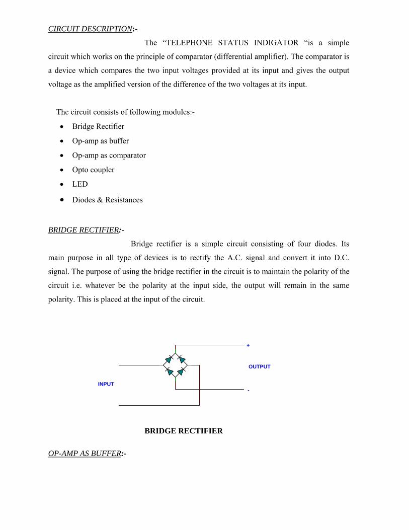
• Diodes & Resistances BRIDGE RECTIFIER:-
Bridge rectifier is a simple circuit consisting of four diodes. Its
main purpose in all type of devices is to rectify the A.C. signal and convert it into D.C.
signal. The purpose of using the bridge rectifier in the circuit is to maintain the polarity of the
circuit i.e. whatever be the polarity at the input side, the output will remain in the same
polarity. This is placed at the input of the circuit.
INPUT
OUTPUT
-
+
BRIDGE RECTIFIER
OP-AMP AS BUFFER:-

This op-amp is placed at output first opto coupler. It is a feedback
amplifier with the gain as unity. Its main purpose is to act as a buffer to the comparator
circuit.
- + +
Opto1 lm324
Feedback
Output Non Inv rting e Input Inverti g n Input
OP-AMP AS BUFFER
OP-AMP AS COMPARATOR:- The comparator is a device which compares the two input
voltages provided at its input and gives the output voltage as the amplified version of the
difference of the two voltages at its input. Its main role in the circuit is to compare the
voltages provided at its input and give appropriate output to the LED’s.
COMPARATOR
OPTO COUPLER:- The opto coupler is used in the circuit to serve various purposes. The
opto coupler works on a very simple principle. It first converts the incoming electrical energy

into optical energy using an LED and then again converts the optical energy back to the
electrical energy using a n-p-n transistor with the optical energy provided at its base.
The opto coupler serves two major purposes in the circuit; acting as an
isolator and acting as a voltage controller. The first opto coupler Opto1 is attached in
between of the bridge rectifier and the remaining circuit. Its main purpose here is to serve as
an isolator. The opto coupler acting as an isolator in the circuit is named as Opto1. The
isolator is used so as to provide an isolated supply to the main circuit. The remaining three
opto couplers Opto2, Opto3 & Opto4 act as the voltage controllers. These are mainly used to
prevent the computer TTL logic family from getting damaged. Since the computer TTL logic
family cannot handle the voltage above 5V but the circuit works at 12V; so to control the
voltage at the input of the computer terminals the opto couplers are used. These opto couplers
are joined in parallel to the LED’s showing the output. The output of the opto coupler is fed
to the parallel ports of the computer.
U1 4N33
OPTO COUPLER
LED:- The LED is a light emitting diode which on application of some voltage across it emits
the light. It is used in the circuit to show the output. LED’s in different colors are used so as
to distinguish the outputs from each other.
- +
LED

DIODES & RESISTANCES:- The various resistances and diodes are used for the protection
purposes. Some resistances are used to make the voltage drops so as to change the reference
voltages at the input of the comparators.
1N1183
DIODE RESISTANCE
WORKING OF CIRCUIT:- The input is provided to the circuit by the incoming telephone
line, by connecting it in parallel to input ports of the device. The voltage provided by the
telephone to the input ports of the device is further given to a full wave bridge rectifier whose
main function is to maintain the polarity. An optocoupler is a device which gives a
completely isolated D.C. supply at its output. It is an optical device which takes the electrical
input converts it to optical form using an LED and finally converts the signal back to
electrical form using a transistor.
The completely isolated electrical supply provided by the optocoupler is given to
the op-amp1, which is a feedback amplifier whose gain is unity. This op-amp acts as a buffer.
The amplified output produced is further fed to another three op-amps, which are the
comparators. The amplified output is fed at the non-inverting terminal of the op-amps. The
inverting terminals of the three op-amps are connected to a 6V D.C. supply through
successive voltage drops across various resistances, a ladder circuit. This voltage provided at
the inverting terminals is known as the reference voltage. The comparators i.e. the op-amps
compare the input at their terminals and give the difference of the two input voltages
amplified with some amplification factor. For the op-amp2 connected with the yellow LED
have the highest reference voltage. The corresponding reference voltage decreases as we
move from op-amp3 (connected to green LED) to the op-amp4 (connected to the red LED).
Now, when the telephone is in working condition i.e. in ideal state, the voltage
provided at the non-inverting terminals of the op-amps will be maximum nearly 45-50V.

With this high voltage at the input terminal the op-amps will give a high voltage output to the
connected LED’s. Since the green and the red LED’s are connected reverse biased hence will
not glow. The yellow LED is connected forward biased with the op-amp hence will glow and
indicate that the telephone is in working condition.
The remaining terminals of the two LED’s (green and red)
are connected to a 6V D.C. supply through Different resistances. Now when the telephone is
dead 0V is at the input of the op-amps hence their output completely depends upon the
reference voltages applied at their respective inputs. In this situation the output voltage
produced at the op-amp3 is relatively more than at the op-amp4. This low voltage at the
output of the op-amp4 make the red LED glow as it become forward biased due to the 6V
D.C. supply (which indicates that the telephone is dead). In this condition the green LED
doesn’t glows as there is considerable drop in the voltage coming from the red LED due the
series resistance and the voltage at the anode of the green LED is small as compared to one
received at its cathode terminal (as the reference voltage at the op-amp3 is more than at op-
amp4).
Now when the voltage lies between the above two situations, the green LED glows
indicating that the telephone is currently in use.
Three optocouplers are attached in parallel to these LED’s so as to give the output to
the computer through parallel port. The basic use of the optocouplers is to save the
computer’s TTL family from getting damaged. The computer works on the voltage levels
varying between 0-5V. Hence if a voltage higher than this is fed to the computer it will be
damaged. So to prevent the computer from being damaged we use optocouplers. These
optocouplers are supplied a voltage supply of just less than 5V. These optocouplers restrict
the output and the required voltage level is provided to the computer input for further
processing.

EXPLANATION FOR
OPERATIONAL AMPLIFIER
OPERATIONAL AMPLIFIER:
An operational amplifier most commonly referred as OP-
AMP. It is a very high gain differential amplifier with high input resistance and high output
resistance. OP-AMP can amplify signals having frequency ranges from 0Hz to a little beyond
1MHz . In other words the OP-AMP can be used to amplify not only DC signals ( 0
frequency ) but also AC signals (high frequency signals ).
The name operational amplifier has been given because it was originally
design to perform mathematical operation. By proper selection of external components,
OP-AMP can be configured to perform a variety of operations such as summation ,
subtraction , multiplication, integration and differentiation .
The IC version of OP-AMP (741 IC ) was introduced in between 1964
and 1968 . With the IC OP-AMP , the circuit design becomes very simple ; moreover it
has the advantage of low cost , take up less space and powers then the discrete components.
Typical uses of OP-AMP are to provide voltage amplitude changes (amplitude
and polarity ) , oscillators , filter circuit and many type of instrumentation circuits .
An OP-AMP contains a number of differential amplifier stages to achieve a
very high voltage gain.
BLOCK DIAGRAM OF AN OP-AMP : The OP-AMP usually consists of four cascaded
blocks as shown in fig.
Non-inverting Input
Inverting
Input Stage
Intermediate Stage
Level Shifting Stage
Output stage
Input Dual input Dual input unbalanced Emitter follower complimentary balanced output output differential using constant symmetry differential amplifier amplifier current source push- pull amplifier

BLOCK DIAGRAM OF OPERATIONAL AMPLIFIER
As shown in fig. OP-AMP consists of two differential amplifiers followed by
level shifter stage and output stage.
The input stage is the dual input , balanced output differential amplifier ,
having a very high open loop gain (without feedback ) . This provides most of the
gain of the amplifier and also established the input resistance of the OP-AMP. The
differential amplifier rejects common noise signals present at the input signals.
The intermediate stage is dual input , unbalanced output differential
amplifier , which is driven by the output of the first stage . The purpose of an intermediate
stage is to provide some additional gain.
Because the direct coupling is used the DC at the output of the intermediate
stage is well above the ground potential. Therefore, usually the level shifting stage is used
after the intermediate stage to shift the DC level at the output of intermediate stage
downward to 0V with respect to ground.
The output is generally a push-pull or push-pull complimentary symmetry
amplifier pair. It increases the output voltage swing , rises the current supplying
capability of OP-AMP and also provides low output resistance .
SYMBOL FOR OPERATIONAL AMPLIFIER: Fig. shows the symbol for an Operational
amplifier, which is simply a triangular shape having two inputs (plus and minus) and a single
output.
+
-
SYMBOL OF AN OP-AMP
The plus ( + ) input produces an output i.e. in phase with the signal (V1) applied to it
, hence this input terminal is called as non-inverting terminal.
While a signal (V2) appearing at minus (-) input terminal result in an inverted output
(opposite polarity output ) hence this input terminal is known as inverting terminal.
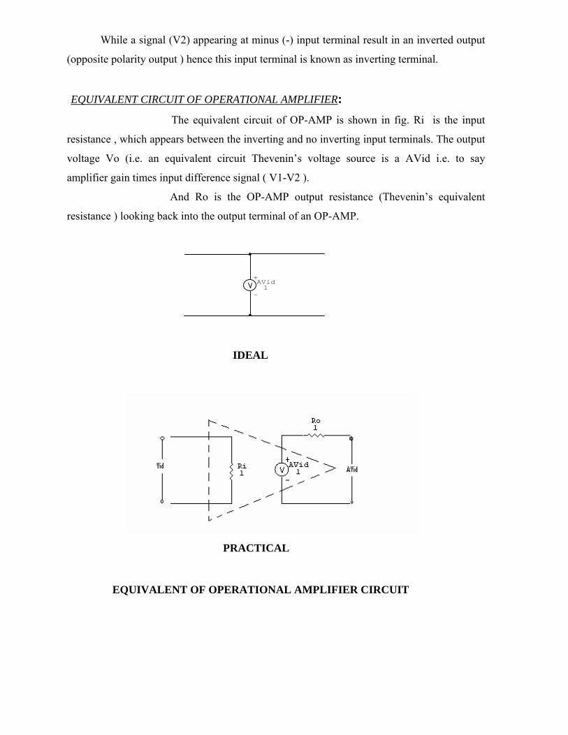
EQUIVALENT CIRCUIT OF OPERATIONAL AMPLIFIER: The equivalent circuit of OP-AMP is shown in fig. Ri is the input
resistance , which appears between the inverting and no inverting input terminals. The output
voltage Vo (i.e. an equivalent circuit Thevenin’s voltage source is a AVid i.e. to say
amplifier gain times input difference signal ( V1-V2 ).
And Ro is the OP-AMP output resistance (Thevenin’s equivalent
resistance ) looking back into the output terminal of an OP-AMP.
+
-
AVid1
IDEAL
PRACTICAL EQUIVALENT OF OPERATIONAL AMPLIFIER CIRCUIT
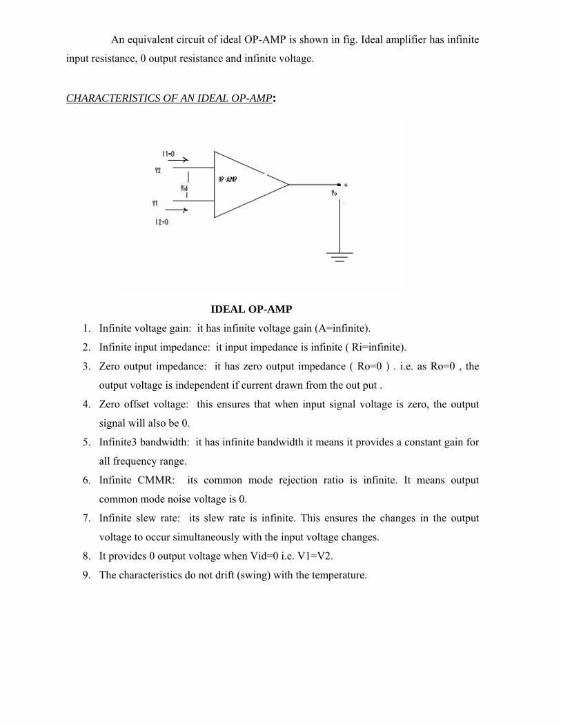
An equivalent circuit of ideal OP-AMP is shown in fig. Ideal amplifier has infinite
input resistance, 0 output resistance and infinite voltage.
CHARACTERISTICS OF AN IDEAL OP-AMP:
IDEAL OP-AMP
1. Infinite voltage gain: it has infinite voltage gain (A=infinite).
2. Infinite input impedance: it input impedance is infinite ( Ri=infinite).
3. Zero output impedance: it has zero output impedance ( Ro=0 ) . i.e. as Ro=0 , the
output voltage is independent if current drawn from the out put .
4. Zero offset voltage: this ensures that when input signal voltage is zero, the output
signal will also be 0.
5. Infinite3 bandwidth: it has infinite bandwidth it means it provides a constant gain for
all frequency range.
6. Infinite CMMR: its common mode rejection ratio is infinite. It means output
common mode noise voltage is 0.
7. Infinite slew rate: its slew rate is infinite. This ensures the changes in the output
voltage to occur simultaneously with the input voltage changes.
8. It provides 0 output voltage when Vid=0 i.e. V1=V2.
9. The characteristics do not drift (swing) with the temperature.

S.NO. CHARACTERISTICS IDEAL OP-
AMP
PRACTICAL 741 IC
OP-AMP
1. Open loop voltage gain(0.A) Infinite 2*10^5
2. Input impedance (Ri) Infinite 2M ohm
3. Output impedance(Ro) 0 75 ohm
4. Input offset voltage 0 2mV
5. Input offset current 0 200nA
6. Bandwidth Infinite 1MHz
7. CMMR Infinite 90dB
8. Slew rate Infinite 0.5 V/micro sec.
OP-AMP AS COMPARATOR: A comparator compares a signal voltage on one input
terminal of the OP-AMP with a reference voltage is applied to other input terminal. The
comparator circuit has only two possible output voltages , which indicate whether the
applied input voltage is greater than or less than the reference voltage.
The simplest type of comparator is basic non-inverting comparator as
shown in fig.
COMPARATOR To construct the comparator OP-AMP is operated in open loop condition. Since
the open loop gain of the OP-AMP goes in to saturation. Thus the to possible output levels of
this comparator are Vsat and -Vsat.
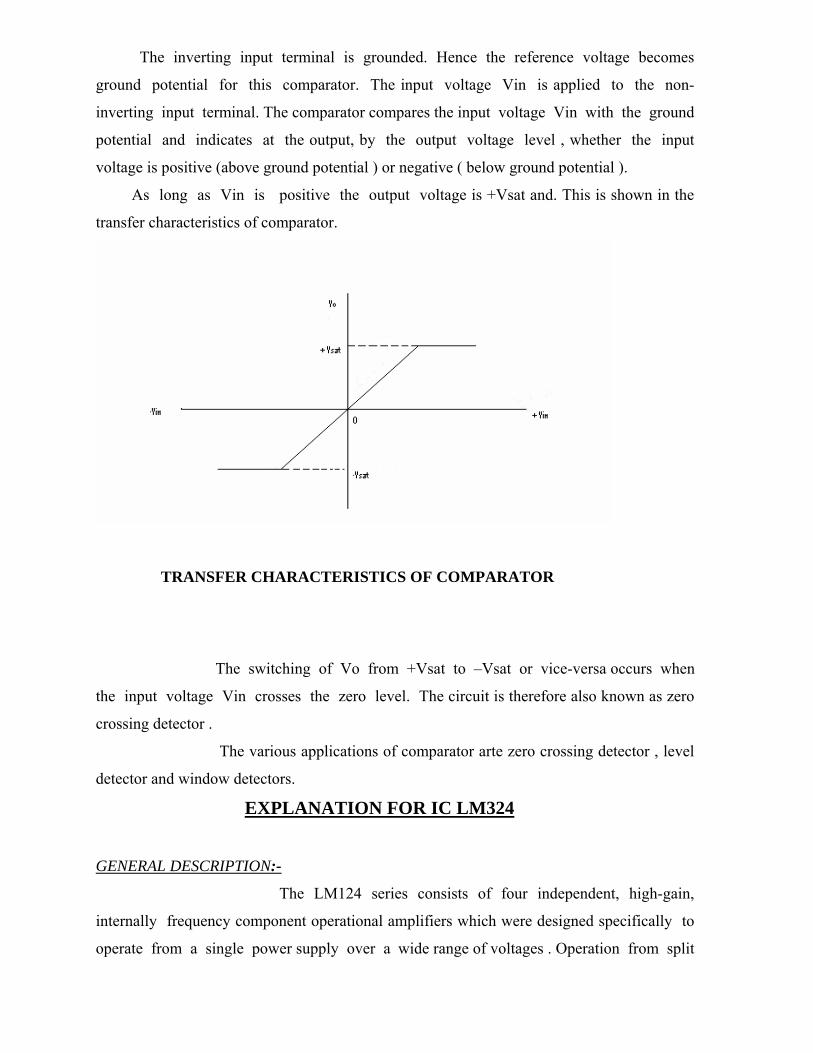
The inverting input terminal is grounded. Hence the reference voltage becomes
ground potential for this comparator. The input voltage Vin is applied to the non-
inverting input terminal. The comparator compares the input voltage Vin with the ground
potential and indicates at the output, by the output voltage level , whether the input
voltage is positive (above ground potential ) or negative ( below ground potential ).
As long as Vin is positive the output voltage is +Vsat and. This is shown in the
transfer characteristics of comparator.
TRANSFER CHARACTERISTICS OF COMPARATOR
The switching of Vo from +Vsat to –Vsat or vice-versa occurs when
the input voltage Vin crosses the zero level. The circuit is therefore also known as zero
crossing detector .
The various applications of comparator arte zero crossing detector , level
detector and window detectors.
EXPLANATION FOR IC LM324
GENERAL DESCRIPTION:-
The LM124 series consists of four independent, high-gain,
internally frequency component operational amplifiers which were designed specifically to
operate from a single power supply over a wide range of voltages . Operation from split

power supplies is also possible & the low power supply current drain is independent of
the magnitude of the power supply voltage.
Application areas include transducer amplifier, DC gain blocks and all the
conventional op amp circuit, which now can be more easily implemented in single power
supply systems. For example LM124 series can be directly operated off of the standard +5v
power supply voltage which used in digital systems and will easily provide the
required interface electronics without requiring the additional +(-)15v power supplies.
UNIQUE CHARACTERISTICS:
• In the linear mode the input common-mode voltage range includes ground and
the output voltage can also swing to ground, even though operated from only a single
power supply voltage.
• The unity gain cross frequency is temperature compensated.
• The input bias current is also temperature compensated.
ADVANTAGES:
• Eliminates need for dual supplies.
• Four internally compensated op amps in a single package.
• Allows directly sensing near GND and Vout also goes to GND.
• Compatible with all forms of logic.
• Power drain suitable for battery operation.
FEATURES:
• Internally frequency compensated for unity gain.
• Large DC voltage gain 100dB.
• Wide bandwidth (unity gain ) 1MHz
(Temperature compensated)
• Very low supply current drains (700MicroAmp.)-essentially
Independent of Supply voltage.
• Wide power supply range :

Single supply 3v to 32v or dual supplies +-1.5vto +-16v.
• Low input biasing current 45nA
(Temperature compensated)
Input common-mode voltage range includes ground.
• Large output voltage swing 0v to v+ -1.5v.
• Differential input voltage range equal to the power supply voltage.
• Low input offset voltage: 2mV and offset current: 5nA
• Large output voltage swing 0V to V+ - 1.5V
PIN CONFIGURATION.
EXPLANATION IC MCT2E (OPTOISO)
DESCRIPTION:
The MCT2XXX series optoisolators consist of a gallium arsenide infrared
emitting diode driving silicon phototransistor in a 6-pin dual in-line package.
Each optocoupler consists of gallium arsenide infrared LED and a silicon NPN
phototransistor. These couplers are Underwriters Laboratories (UL)listed to comply with a
5300 VRMS isolation test voltage.
APPLICATION:
• Power supply regulators

• Digital logic inputs
• Microprocessor inputs
• AC mains detection
• Reed relay driving
• Switch mode power supply feedback
• Telephone ring detection
• Logic ground isolation
• Logic coupling with high frequency noise rejection
FEATURES:
• UL recognized (File # E90700)
• VDE recognized (File # 94766)
-Add option V for white package (e.g., MCT2V-M)
-Add option 300 for black package (e.g., MCT2.300)
• Interfaces with common logic families
• Input-output coupling capacitance < 0.5 pF
• Industry Standard Dual-in line 6-pin package
• MCT2 and MCT2E are also available in white
package by specifying -M suffix, eg. MCT2-M
SCHEMATIC:

PIN:
1. Anode
2. Cathode
3. No connection
4. Emitter
5. Collector
6. Base
INTRODUCTION TO PARALLEL PORT
In computers, ports are used mainly for two reasons: Device control and
communication. We can program PC's Parallel ports for both. Parallel ports are mainly meant
for connecting the printer to the PC. But we can program this port for many more
applications beyond that.
The general digital communication between the computer and other hardware can be
done via two ways: -
1) Serial ports and
2) Parallel ports
Among the above two communication medias the parallel ports are much faster than
serial ports.
Parallel ports are easy to program and faster compared to the serial ports. But main
disadvantage is it needs more number of transmission lines. Because of this reason parallel
ports are not used in long distance communications. Let us know the basic difference
between working of parallel port and serial port. In serial ports, there will be two data lines:
One transmission and one receive line. To send a data in serial port, it has to be sent one bit
after another with some extra bits like start bit, stop bit and parity bit to detect errors. But in
parallel port, all the 8 bits of a byte will be sent to the port at a time and an indication will be
sent in another line. There will be some data lines, some control and some handshaking lines
in parallel port.

Usually ports are found on the rear of computer and are of the following two types:-
1) Male ports
Having pins coming out of port.
2) Female ports
Having holes for pins.
• Parallel port is generally a 25 pin female connector with which a printer is usually
attached.
COMMUNICATION BETWEEN THE COMPUTER AND THE PRINTER :-
For the communication between PC and printer takes place. Computer places the
data in the data pins, and then it makes the strobe low. When strobe goes low, printer
understands that there is a valid data in data pins. Other pins are used to send controls to the
printer and get status of the printer; these can be understood by the names assigned to the
pins.
To use the printer port for applications other than printing, we need to know how
ports are organized.
THERE ARE THREE REGISTERS ASSOCIATED WITH LPT PORT:
1) Data register,

2) Control register and
3) Status registers.
Data register will hold the data of the data pins of the port. That means, if
we store a byte of data to the data register, that data will be sent to the data pins of the port.
Similarly control and status registers. The following table explains how these registers are
associated with ports.
PIN NO (D-TYPE 25) SPP SIGNAL DIRECTION
IN/OUT REGISTER.BIT
1* nStrobe In/Out Control.0
2 Data 0 In/Out Data.0
3 Data 1 In/Out Data.1
4 Data 2 In/Out Data.2
5 Data 3 In/Out Data.3
6 Data 4 In/Out Data.4
7 Data 5 In/Out Data.5
8 Data 6 In/Out Data.6
9 Data 7 In/Out Data.7
10 nAck In Status.7
11* Busy In Status.6
12 Paper-Out / Paper-End In Status.5
13 Select In Status.4
14* nAuto-Linefeed In/Out Control.1
15 nError / nFault In Status.3
16 nInitialize In/Out Control.2
17* nSelect-Printer/ nSelect-In In/Out Control.3
18 – 25 Ground Gnd
Pins with * symbol in this table are hardware inverted. Than means, If a pin has a
'low' i.e. 0V, Corresponding bit in the register will have a ‘high’ .

Signals with prefix 'n' are active low. That means, Normally these pins will have
low value. When it needs to send some indication, it will become high. For example,
normally nStrobe will be high, when the data is placed in the port, computer makes that pin
low.
Normally, data, control and status registers will have following addresses. We
need these addresses in programming later.
Register LPT1 LPT2
Data register (Base Address + 0) 0x378 0x278
Status register (Base Address + 1) 0x379 0x279
Control register (Base Address + 2) 0x37a 0x27a
IN TURBO C, THERE ARE FOLLOWING FUNCTIONS USED FOR ACCESSING THE
PORT:
• out port( PORTID, data);
• data = inportb( PORTID);
• outport( PORTID, data);
• data = inport( PORTID);
Outport ( ) function sends a word to port, inport( ) reads a word from the port.
outportb( ) sends a byte to port and inportb( ) reads a byte from the port. If you include
DOS.H header, these functions will be considered as macro, otherwise as functions. Function
inport( ) will return a word having lower byte as data at PORTID and higher byte as data at
PORTID+2. So, we can use this function to read status and control registers together.
inportb( ) function returns byte at PORTID. outport( ) writes the lower byte to PORTID and
higher byte to PORTID+1. So this can be used to write data and control Together. outportb( )
function writes the data to PORTID. outport( ) and outportb( ) returns nothing.
PROGRAM TO SHOW THE TELEPHONE STATUS ON THE
COMPUTER SREEN USING PARALLEL PORTS

#include<stdio.h>
#include<conio.h>
#include<dos.h>
#include<process.h>
#define PORT 0x378
int data,data1,m,a[8],i,l,c=176,d=219;;
FILE *fp;
void readfile()
{
char ch;
if(fp==NULL)
printf("\n\n\t Sorry some internal error occured");
else
{
ch=getc(fp);
if(ch==EOF)
{
printf("\n\n\t\t\t Log file empty");
delay(1500);
l=1;
}
else
{
rewind(fp);
i=0;
printf("\n\t\t DATE \t\t\t TIME");
printf("\n\t\t ---- \t\t\t ----\n");
while(1)
{

i++;
ch=getc(fp);
if(i==432)
{
printf("\n\n\n PRESS ANY KEY TO CONTINUE....\n\t\t");
getch();
clrscr();
printf("\n\t\t DATE \t\t\t TIME");
printf("\n\t\t ---- \t\t\t ----\n");
i=0;
}
if(ch==EOF)
break;
printf("%c",ch);
}
}
}
}
void filerecord()
{
char choice;
fp=fopen("LOG.TXT","r");
l=0;
readfile();
if(l!=1)
{
printf("\n\n\t Do you want to erase the previous log records(y/n)->");
fflush(stdin);
scanf("%c",&choice);

if((choice=='Y')||(choice=='y'))
{
fclose(fp);
fopen("LOG.TXT","w");
clrscr();
gotoxy(5,8);
printf("\n ERASING...");
gotoxy(5,12);
for(i=0;i<50;i++)
printf("%c",c);
gotoxy(5,12);
for(i=0;i<50;i++)
{
delay(50);
printf("%c",d);
}
gotoxy(5,14);
printf(" All the records have been erased");
delay(1500);
}
}
fclose(fp);
clrscr();
}
void writefile(void)
{
struct date d;
struct time t;
getdate(&d);
gettime(&t);
fp=fopen("LOG.TXT","a");
if(fp==NULL)

{
printf("\n\n\t SORRY SOME INTERNAL ERROR OCCURED WHILE OPENING LOG
FILE");
}
else
{
fprintf(fp,"\n\t\t%d-%d-%d\t\t\t%2d:%2d:%2d
",d.da_day,d.da_mon,d.da_year,t.ti_hour,t.ti_min,t.ti_sec);
}
fclose(fp);
}
void getstatus()
{
data1=0;
while(!kbhit())
{
data=inport(PORT+1);
if(data!=data1)
{
delay(100);
m=data;
i=0;
while(m>0)
{
a[i++]=m%2;
m=m/2;
}
if(a[3]==1)
{
clrscr();

printf("\n\n\n\t TELEPHONE STATUS :- Phone is dead");
printf("\n\n\n Please press 'THE DOWN ARROW KEY' to exit scanning of
telephone status");
}
else if(a[4]==1)
{
clrscr();
printf("\n\n\n\t TELEPHONE STATUS :- Phone is idle");
printf("\n\n\n Please press 'THE DOWN ARROW KEY' to exit scanning of
telephone status");
}
else if(a[5]==1)
{
clrscr();
printf("\n\n\n\t TELEPHONE STATUS :- Phone is currently in use");
printf("\n\n\n Please press 'THE DOWN ARROW KEY' to exit scanning of
telephone status");
writefile();
}
}
data1=data;
}
}
void main()
{
int ch;
clrscr();
gotoxy(20,12);
printf("Welcome to the Telephone Status Software");
gotoxy(20,13);
printf("----------------------------------------");

delay(3000);
clrscr();
while(1)
{
delay(100);
printf("\n\n\n\n\t\tMENU");
printf("\n\t\t----");
printf("\n\n\t1.Read the current telephone status");
printf("\n\t2.Previos log file");
printf("\n\t3.Exit the software");
printf("\n\n\t Please enter the choice : -");
scanf("%d",&ch);
switch(ch)
{
case 1:getstatus();
clrscr();
break;
case 2:clrscr();
printf("\n\n\t\t\t\t LOG FILE");
printf("\n\t\t\t\t---------\n\n");
filerecord();
break;
case 3:exit(0);
default:printf("\n\n\t Please enter a valid choice!");
}
if((ch<1)||(ch>3))
{
delay(1000);
clrscr();
}
}
}

PARTS SPECIFICATION:-
RESISTOR :- ±5%
R1 → 33k
R2 → 1k
R3 → 3.9k
R4 → 4.7k
R5 → 3.3k
R6 → 4.7k 60% (var. resist.)
R7,R8,R9,R10,R11,R12 → 10k
R13,R14 → 760 ohm
R15 ,R16,R17,R18→ 1k
SEMICONDUCTOR:-
D1 → Bridge
D2,D3,D4,D5,D6,D7,D8,D12,D13 →1N4148
D9 → Yellow L.E.D.
D10 → Green L.E.D.
D11 → Red L.E.D.
IC’S:-
LM324 → OP-AMP IC
MCT2E → OPTOCOUPLER IC

CONCLUSION
I would like to conclude this training as a very great and enriching experience.
During the training I familiarized myself with P.C.B designing, application of
I.C. (its pin diagram), mounting of components using soldering process and interfacing of the
hardware circuit with the computer.
The circuit can be used at all places starting from domestic to the industrial
sectors. The simplicity in the usage of this circuit helps it to be used by a large number of
people as people with less knowledge of hardware can also use it without facing any
problem. The time to time checking the status of the telephone lines leads to the successful
maintenance of the internet connection.
I also learned about the engg. responsibility and about their hard work . This
training was not only good for personality development but also great in terms of imparting
practical knowledge.
Thus I conclude our training with a very nice and wonderful experience gained at
DRDO, Jodhpur, under a peaceful kind and friendly environment.
BIBLIOGRAPHY
• OP-AMP and linear integrated circuit- RAMAKANT.K.GAYAKWAD
• http/ www.google.com
• http/ www.electrosofts.com
• Electronics For You edition (June 2006).