precision antenna measurement guide - test-italy.com antenna measurement guide e-book september 2017...
TRANSCRIPT

S P O N S O R E D B Y
Precision Antenna Measurement Guide
E -BO O K
September 2017

Table of Contents
2
3 IntroductionPat HindleMicrowave Journal, Editor
4 Basic Rules for Anechoic Chamber Design, Part One: RF Absorber ApproximationsVince RodriguezMI Technologies
10 Basic Rules for Anechoic Chamber Design, Part Two: Compact Ranges and Near Field MeasurementsVince RodriguezMI Technologies
22 Characterizing and Tuning Antennas Using an Automated Measurement System and a VNACopper Mountain TechnologiesDiamond Engineering
Copper Mountain Technologies
Application Profile As the number of devices featuring wireless connectivity
grows, ensuring their performance specifications while staying within regulatory requirements becomes even more important. Antenna pattern measurement is a critical step in the design process of antennas and wireless devices. Compact antenna measurement systems combined with a high performance VNA are necessary to characterize parameters such as pattern, gain, VSWR, and efficiency. These results are used to validate simulated designs and identify possible performance issues before final testing. By using an in-house measurement system, multiple design revisions can be tested and pre-certified without the high cost of using an accredited or certified measurement facility for each test. Other considerations like portability and low cost are important to engineers in various environments like defense or education, respectively.
ChallengesMaking accurate antenna measurements carries a number
of challenges, some of the most important being dynamic range, calibration, and speed. A sufficient dynamic range will allow the antenna to be measured accurately at both minimum and maximum signal level with a minimal amount of trace noise. Older network analyzers can reach a reasonable dynamic range and reduced noise by reducing the IF bandwidth but the analyzer speed is greatly reduced, a single sweep can take many seconds to complete. PC-based VNA’s offer the benefit of greater initial dynamic range, higher speeds, and direct data transfer.
Application: Characterizing the AntennaIn this example, an unknown 2.4 GHz antenna is
characterized, with a configuration consisting of: Diamond Engineering DAMS 5000 positioner with an FSM spherical mount, RF cables, a calibrated reference antenna, a Copper Mountain Technologies Planar 804/1 VNA, and a computer (PC) running the measurement and VNA software. To begin, the VNA is set to the antenna's frequency range, all RF cable loss (including positioner) is calibrated out using the VNA’s built in 12 term calibration. Once the calibration is complete the AUT is mounted to the positioner’s RF Rotary Joint and the reference antenna is connected then positioned at the appropriate distance (typically 1 or 3 meters). Now that the antennas are connected and the VNA is set to transmission (S
12 or S
21), the
VNA will show the response of the entire link. At this point the user can note the signal response on the analyzer; if the polarization is correct and the AUT is at a point of high signal,
the VNA should show a strong profile with little trace noise. Depending on the type of antenna being measured, the antenna can be manually positioned
to a point of lowest signal to confirm that the signal is still above the noise floor and the trace noise is acceptable for testing requirements. After the setup is verified, the DAMS antenna measurement software is used to make a measurement. The software indexes the antenna to every physical point and executes a transmission sweep on the VNA. Optionally, VSWR data can be automatically collected at every point. Once complete, the entire data set can be viewed,
processed and exported.
Characterizing and Tuning Antennas Using an
Automated Measurement System and a VNAAPP NOTE
Precision RF Cables
The full DAMS setup
Scalar or Vector* Calibration(* Requires VNA)
DAMS Positioner / AUT
Controller
DAMS Antenna Measurement Studio
USBGPIB / Ethernet / USB
VNA, Rec. Only or Source/Receiver
25 Practical Antenna Connection for Accurate TestingClayton Karmel, Pdicta Corp.; Ben Maxson, Copper Mountain
15 Extending the Quiet Zone Using an RF Lens on a Conical Tapered Chamber to 18 GHzV. Rodriguez, ETS-Lindgren L.P.; S. Matitsine, Matsing Pte. Ltd. and Temasek Laboratories, National University of Singapore; T.T. Chia, DSO National Laboratories and Temasek Laboratories, National University of Singapore; P. Lagoiski, L. Matytsine and M. Matytsine, Matsing Pte. Ltd.; P.K. Tan, Temasek Laboratories, National University of Singapore

3
Introduction
Antennameasurementsaredifficulttomakeduetotheirmulti-directionalnature,theircables/connectionstoequipmentandinterferingsignalsintheenvironment.Themeasurementsetup,surroundingenvironmentandphysicalconnectionsallneedtobecarefullyspecifiedandsetup,payingcloseattentiontotheinstrumentsandmaterialsused. AnechoicchambersareakeyelementinthemeasurementsystemsothefirstthreearticlesinthiseBookdiscusschamberdesignincludingcompactrangesandnearfieldmeasurements.Whiletherearesomearticlesandbooksthataddressanechoicchamberdesign,therearefewconcisearticlessummarizingtheirdesignandsimplerulesofthumb.ThefirstarticleinthiseBookcoverschamberdesignandrecommendsthepropertypeofrangefordifferentantennatypesandfrequenciesofoperation.Rulesofthumbareprovidedtoselectthebestapproachfortherequiredtestorantennatype.Thearticleconcentratesonrectangularchamberswithsimpleapproximationsusedforabsorberperformancetogenerateaseriesofchartsthatcanbeusedasaguidetospecifyperformanceandappropriatefacilitysize.Italsodiscussesthelimitationsinusingfarfieldchambers,mainlyrelatedtotheelectricalsizeofantennasthatcanbetested. Thesecondarticleisparttwobythesameauthorandcoverscompactrangesandnearfieldmeasurementsasasolutiontothelimitationsoffarfieldchamberscoveredinpartone.ThethirdarticlediscussesextendingthequietzoneusinganRFlensonaconicaltaperedchambersotheseriesofthreearticlescoveralotofgroundonthesubjectonanechoicchamberdesignandtechnology. Makingaccurateantennameasurementshasanumberofchallenges,someofthemostimportantbeingdynamicrange,calibration,andspeed.CompactantennameasurementsystemscombinedwithahighperformanceVNAarenecessarytocharacterizeparameterssuchaspattern,gain,VSWR,andefficiency.ThefourtharticlecoversantennapositioningandVNAsetupforautomatedmeasurementsusedtovalidatesimulateddesignsandidentifypossibleperformanceissuesbeforefinaltesting. ConnectingRFtestandmeasurementequipmenttoanantennaundertestusuallyinvolvestradeoffsamongmeasurementaccuracy,electricalconsiderations,costandmechanicalruggedness.InthefinalarticleofthiseBook,aspectsoftheantennaconnectionarecoveredwithpracticaladviceforsuchtestandmeasurementscenarioswithacompactWiFimoduleexample.WehopethiseBookwillgiveyouthetechnicalknowledgeandbackgroundtohelpyoudesigntestsystemsandaccuratelymakeantennameasurements.
Pat Hindle,MicrowaveJournalEditor

4
Basic Rules for Anechoic Chamber Design, Part One: RF Absorber ApproximationsVince RodriguezMI Technologies, Suwanee, Ga.
The task of adequately specifying performance for an indoor anechoic chamber without driving unneces-
sary costs or specifying contradictory re-quirements calls for insight that is not al-ways available to the author of the speci-fication. While there are some articles and books1-3 that address anechoic chamber design, a concise compendium of refer-ence information and rules of thumb on the subject would be useful. This article intends to be a helpful tool in that regard. It starts by recommending the proper type
of range for different antenna types and frequencies of operation. Rules of thumb are provided to select the best approach for the required test or antenna type. The article concentrates on rectangular cham-bers. Simple approximations are used for absorber performance to generate a se-ries of charts that can be used as a guide to specify performance and appropriate facility size.
The ability to measure an antenna is an important design requirement in determin-ing if energy is radiating properly and in the desired direction, as well as how much en-ergy is traveling in undesired directions. To measure antennas (like many other devices that are being measured), there is the de-sire to have the antenna unaffected by its surrounding environment. This is where the anechoic chamber becomes a viable solu-tion. The anechoic chamber provides an environment free of echo or other radiated signals to reduce the effects of these unde-sirable signals.
This article covers applications where an antenna is radiating or receiving a given signal, and its performance as a function of direction is being measured. s Fig. 1 General geometry of an indoor range - two antennas are locat-
ed in the range (one for transmitting and one for receiving).

s Fig. 2 The far field distance plotted related to the wavelength.
1000500300200100
50302010
5321
2018161412108642D/�
r/�
TABLE IFREQUENCY RANGES AND ANTENNA SIZES FOR THE DIFFERENT INDOOR ANTENNA
MEASUREMENT APPROACHES
Indoor Ranges Antenna Size in Wavelengths
Frequency Far Field Illumination
Near Field Compact Range
100 MHz <2 >2 Not ideal
500 MHz <2 >2 Not ideal
1 GHz <5 >5 >5
2 GHz <10 >10 >10
≥ 4 GHz <10 >10 >10
5
indoor measurements at those low frequencies. Indoor ranges can be built, but the antenna size should be kept less than 2; which limits the far field distance to 8 (24 m). This distance is close to the 10 given by Equation 2. Table 1 pro-vides an approximate guide for the different antenna sizes and fre-quencies of operation.
The values in Table 1 are gen-eral guidelines. Spherical near field (SNF) ranges can test antennas as small as /2. But for such a small an-tenna it may be a better approach to use a far field illumination range as it relates to the typical electrical size of the AUT.
When creating an anechoic chamber, the goal is to obtain a volume in the chamber where any reflected energy from the walls of the range (ceiling and floor) will be much lower than any of the features of interest on the radiation pattern. This volume is known as the quiet zone (QZ). Figure 1 shows that as one antenna transmits, it illumi-nates the receive antenna and all the walls and surfaces of the range. The energy incident onto these sur-faces will be reflected towards the QZ.1,3 The level of reflected energy must be a given number of deci-bels below the direct path between the transmitting and receiving an-tennas.
As the antenna being measured is rotated (see Figure 3), its main beam will illuminate different sur-faces of the chamber. The range antenna will measure the level of field radiated by the AUT along the direct path between the two antennas. However, the range an-tenna will also receive the reflected energy from the walls, ceiling and floor. If the reflected energy level is higher than the energy radiated along the direct path between the two antennas, then the radiation pattern in that direction cannot be measured accurately. In Figure 3, the measuring antenna, (also known as range antenna or source antenna) is pointing at a null, but it is also receiving the reflected sig-nal from the wall that is illuminated by the main beam of the AUT. The range antenna is receiving the re-flected signal in a direction of 30°. In that 30° direction, the gain of
RANGE TYPE SELECTIONThe general range geometry
is shown in Figure 1. There are several methods of measuring the radiation patterns of antennas in-doors: far field illumination, near field measurements and compact range. While they all present pros and cons, there is not a single so-lution that is ideal for all types of antennas and situations. The type of range most suitable for a given type of antenna is driven by two parameters: frequency and elec-trical size of the antenna under test (AUT). The far field condition given by the following equation drives the selection:
r2D
(1)2
≥λ
The parameters mentioned above are embedded into the far field equation. D is the largest physical dimension of the antenna. Wavelength is , which is related to the frequency of operation on the antenna. For smaller antennas the far field range length, r, can be ap-proximated by:4
r 10 (2)≈ λ
This equation can be used when the antenna is under one wave-length in electrical size. From Equa-tion 1, the far field distance can be plotted as a function of the electri-cal size of the antenna, as shown in Figure 2.
As a rule of thumb for indoor ranges, the far field illumination techniques are better suited for antenna sizes under 10. This rule is related to the electrical antenna size. Frequency of operation adds another factor that will influence the type of range. An antenna with
a size of 10 will have a far field distance of 200, making the test distance 20 times the size of the an-tenna. At some microwave frequen-cies this may be a test distance of 200 inches (5 m) so an indoor range may be easy to implement. How-ever, note a 20 antenna will have a test distance that is 800.
For example, consider an 18 inch dish used by a popular satellite TV service. This satellite service oper-ates at 18.55 GHz. The dish anten-na is 28.29 in size. The far field is at approximately 1600 or 25.86 m (84.84 ft). Clearly, for such an elec-trically large antenna, a far field il-lumination approach indoors is not economically feasible. For this an-tenna, a compact range or a near field approach is more suitable. Conversely, a 10 antenna at 300 MHz, which is 10 m in size, would be extremely difficult to manipulate at a test distance of 200 m. For this case, the best solution would be an outdoor range.
In general, for frequencies be-low 100 MHz, an outdoor range is a better approach. Current absorber technology does not support some

6
0.25 t 20. This approximation can be used to get a conservative reflectivity value of an absorber of a given thickness. Most manufactur-ers provide the information in their datasheets.
Figure 1 shows that some of the absorber in the range is not located in the normal incident wave direction, but rather in an oblique incidence. For oblique incidence, the main reflectivity of the absorber is in the bi-static direction. Backscattering occurs when the distance between the tips of the pyramids is .7 Hem-ming1 provides plots that show the estimated bi-static reflectivity of absorber at oblique incidence. A series of polynomial approxi-mations, together with Equation 3, provide a general description of the performance of pyrami-dal absorbers of different thick-nesses and at different angles of incidence. These are conserva-tive approximations. That leaves a margin of error to account for things like lights, doors, position-ing equipment and edge diffrac-tions from treatment discontinui-ties.
The absorber performance in dB is given by the following polyno-mial:
R (t, ) R (t) A (t) A (t)A (t) A (t) A (t) (4)
o 1 22
33
44
55
θ = + ⋅θ + ⋅θ+ ⋅θ + ⋅θ + ⋅θ
θ
the range is lower than in the di-rect path (boresight) to the AUT. The reflected energy is a number of dB lower, for example, 20 dB. Let us assume that the gain in the 30° direction is 10 dB lower than the boresight. The signal received by the antenna on that direction will be -30 dB compared to the energy received when the main beam of the AUT was pointing to the range antenna. If the null is less than -30 dB, the measured pattern will have errors.5
RF ABSORBERA key design item for an an-
echoic chamber is the RF absorber. The absorber treatment must be such that the reflected energy has a small or negligible effect on the measured data. A typical RF ab-sorber is a lossy material shaped to allow for incoming electromagnetic waves to penetrate with minimal reflections. Once the electromag-netic (EM) energy travels inside the material, the RF energy transforms into thermal energy and dissipates into the surrounding air.6 The electrical thickness of the material determines how much energy is absorbed. The reflection level at normal incidence can be approxi-mated by the following equation:R (t) 13.374 ln(t) 26.515 (3)o = − −
where t is the thickness in wave-lengths. The equation is valid for
s Fig. 3 An indoor range showing one of the reflected paths and the direct path between the AUT and the source antennas.
Antenna BeingTested (Transmitting)
MeasuringAntenna (Receiving)
The coefficients in this equa-tion are functions of the thickness. When the thickness of the absorb-er is such that 0.25 t 2, the coefficients of Equation 4 are giv-en by the following polynominals:
A (t) 1.5252 4.8243t 6.9479t3.8332t 0.7333t (4a)
A (t) 0.0754 0.24782t 0.3984t0.2285 0.0442t (4b)
A (t) 0.0016 0.00502t 0.00938t0.00577t 0.001155t (4c)
A (t) 1.58 10 4.91 10 t1.015 10 t 6.58 10 t1.35 10 t (4d)
A (t) 5.84 10 1.78 10 t4.02 10 t 2.71 10 t5.7 10 t (4e)
12
3 4
22
4
32
3 4
45 5
4 2 5 3
5 4
58 7
7 2 7 3
8 4
= − +− +
= − + −+ −
= − +− +
= − ⋅ + ⋅− ⋅ + ⋅− ⋅
= ⋅ − ⋅+ ⋅ − ⋅+ ⋅
− −
− −
−
− −
− −
−
When the thickness of the treat-ment is such that 2 t 20, then the coefficients are given by the set of polynominals:
A (t) 0.1751 0.149t0.0119t 0.00028t (4f)
A (t) 0.0105 0.00824t0.0007t 1.61 10 t (4g)
A (t) 0.00029 0.000123t1.13 10 t 2.57 10 t (4h)
A (t) 1.69 10 4.77 10 t5.08 10 10 t 1.14 10 t (4i)
A (t) 0 (4 j)
12 3
22 5 3
35 2 7 3
46 7
8 8 2 9 3
5
= + −+
= − − +− ⋅
= +− ⋅ + ⋅
= − ⋅ − ⋅+ ⋅ − ⋅
=
−
− −
− −
− − −
The domain of Equation 4 is lim-ited by those angles of incidence where 0° 85°and where =0° is normal incidence. Addi-tionally, the domain is limited by the domain of the coefficient poly-nomials. Hence Equation 4 is valid when 0.25 t 20. The range of Equation 4 should also be lim-ited to -55 R(dB) 0. For an ab-sorber thickness larger than 20, the reflectivity can be approximat-ed using the results for a 20 thick absorber. Figure 4 shows the bi-static performance as a function of angle for a series of different elec-trical thickness of the absorber.

7
Figure 5 shows a comparison of computed results using the meth-od in reference 8, a given manu-facturer specifications and the re-sults from Equation 4 for a material of thickness equal to and 2. If the results of the polynomials pre-sented here are compared to those from numerical computations, the polynomials appear to provide a conservative number for the re-
flectivity — higher by about 10 dB. The manufacturer specifications were only provided from 45° to 80° and normal incidence. Computed results were obtained only at a few angles. For the 1 thick absorber, the different methods follow simi-lar trends, with the polynomials providing the most conservative number. There is a large difference at 35° between the computed and the polynomial results. However, that null in the reflectivity may shift depending on the material on which the absorber is mounted.9 In general, the polynomials are a safe approximation for the performance of RF materials at different angles of incidence.
The largest typical absorber size currently available is 72” (1.82 m). This size provides a frequency limit for the use of indoor ranges. At 100 MHz, the thickness of this absorber is 1.64 with a normal incidence performance at about -33 dB. In an indoor range lined with this mate-rial, pattern features -20 dB from the peak will be difficult to mea-sure accurately. There are hybrid absorbers merging ferrite tiles and lossy substrate pyramids of wedg-es that operate down to 30 MHz or even 20 MHz. These are more
suitable for EMC applications as their normal incidence absorption is typically limited between 25 and 35 dB.
RECTANGULAR FAR FIELD CHAMBERS
Sizing the range begins with rectangular far field ranges that have a test distance is determined by Equation 1. It is common to find sources stating the rules of thumb for sizing a rectangular anechoic chamber for far field illumination. Generally, the width and height of an anechoic chamber should be three times the diameter of the minimum sphere that contains the largest antenna being tested. It is important to check that a mini-mum spacing of 2 between the AUT and the tips of the absorber is maintained to avoid loading of the AUT. The far field distance is given by:
r2n (5)2
λ=
Where n is the number of wave-lengths in size of the AUT. The QZ must be large enough to encom-pass the AUT. Hence the QZ is n. Figure 6 shows a typical rect-angular range geometry. From the geometry, an equation for the distance x can be derived. The distance x is the distance from the range centerline to the absorber tips.
xn cot (6)2
λ= ⋅ θ
Equation 6 gives the distance in terms of wavelengths. In Figure 3, the value of can be chosen for a desired reflectivity. The curves in Figure 4 will also provide a value for the thickness of the absorber. Hence, if the AUT has features that need to be measured in the -25 dB level, the bi-static reflectivity of the absorber must exceed that level. Absorber 2 in thickness will exceed -25 dB up to angles of 50°. Hence the width of the chamber is
2x 2n (0.84) 4 (7)2( )= + λ
Where the added 4 accounts for the 2 thickness of the absorber. If a different thickness of absorber
s Fig. 4 Estimated reflectivity of RF absorber as a function of angle of incidence.
0
–5
–10
–15
–20
–25
–30
–35
–40
–45
–50
–55
Thickness in �
8580757065605550454035302520151050Angle of Incidence (°)
Bi-static Reflectivity of Pyramidal Absorber
Ref
lect
ivit
y (d
B)
0.250.511.21.41.51.61.822.53456789101520
s Fig. 5 Comparison of bi-static reflec-tivity from a computational approach, manufacturer’s specifications and Equa-tion 4.
0
–5
–10
–15
–20
–25
–30
–35
–40
–45
–50
–550 10 20 30 40
Angle of Incidence (°)50 60 70 80
1� Equation 42� Equation 41� Computed TL Approximation2� Computed TL Approximation1� Manufacturer A Specs2� Manufacturer A Specs
Ref
lect
ivit
y (d
B)

AUT illumination rather than reduc-ing its level as it is done in the rect-angular chamber. This leads to a physically smaller chamber.
The height of the chamber should be the same as the width. By doing this, the reflections from the ceiling and floor will be similar in level. This is important since the reflected energy from the ceiling and floor will be similar, and the effects of the range on polariza-tion dependant parameters such as cross polarization and axial ratio will be minimized.
Equations 8 and 9 provide a good idea of the space require-ments for an indoor range. In most cases, a chamber size can be ad-justed. For example, the absorber on the ceiling and floor can be in-creased in thickness to maintain the reflectivity at more oblique angles of incidence (larger ). Chebyshev arrangements13 of the absorber layout can also be used to improve reflectivity.
Figure 3 also reveals another clue to improve reflectivity. The re-flected ray arrives at the range an-tenna at an angle at which the gain of the antenna is lower than in the boresight direction. Using higher directivity antennas as sources re-duces the amount of energy re-ceived from the side walls, ceiling and floor. Hence, shorter absorbers reduce the chamber size.
CONCLUSIONPart one of this two-part series
has dealt mainly with approxima-tions for bi-static reflectivity of RF absorbers and the rectangular de-sign of rectangular RF anechoic chambers. The polynomial equa-tions include a “margin of safety” in their results. This helps in account-ing for secondary bounces and edge diffractions as well as light fixtures, vents, doors and other dis-ruptions of the absorber treatment. Part two will provide equations for compact ranges and near field to far field ranges.
ACKNOWLEDGMENTThe author will like to thank
Zhong Chen for providing the com-puted results based on the NIST al-gorithm.8 n
mounting and connecting the an-tenna, switching range antennas, etc. The space should be checked to allow for people to perform these tasks inside the anechoic range.
Expected chamber sizes can be examined by entering values into previous equations. It will be as-sumed that the source antenna is the directive with a sufficient front-to-back ratio. The absorber behind the source antenna will be one wavelength in thickness and the factor K will be set to 4.
In Figure 7, the width and length of a series of rectangular chambers have been plotted versus the low-est frequency of operation. In ad-dition the electrical size of the AUT at the lowest frequency is indicated by the value of n for each chamber size plotted.
If a chamber is designed for an antenna of a given n at the low-est frequency, that same chamber is large enough for testing anten-nas of the same electrical size at higher frequencies. Similarly, as the frequency is lowered, the chamber size must increase. At 500 MHz, a chamber for a 2 sized antenna is about 10 × 5 m. If the antenna size was increased to 4, the chamber would need to be 18 × 10 m. Ta-pered anechoic chambers should be used at these lower frequen-cies.1,10-12 The geometry of the taper chamber uses the specular reflection off the side walls for the
is used, Equation 7 will change. In general, the chamber width can be written as
W 2n cot( ) 2t (8)2( )= θ + λ
Parameters and t must be cho-sen to obtain the required reflectiv-ity. It is important to keep a mini-mum 2 spacing from the QZ to the absorber. The length of the rectan-gular far field chamber is mainly given by the far field distance and the QZ size plus the absorber thick-ness. Added space should be in-cluded for the range antenna and the absorber behind it.
The total chamber or range length (L) is given by:L 2n n 2 t K (9)2( )= + + + + λ
where K is a factor large enough to include the source antenna, the 2 spacing, and the absorber behind the source. It should be noted, that these equations provide a mini-mum requirement. Work must be performed inside the chamber —
s Fig. 6 Geometry of a far field range.
2n2�
n�
x
�
s Fig. 7 Rectangular far field chambers for different lowest frequencies of operation and different largest size antennas at their lowest frequencies.
50
45
40
35
30
25
20
15
10
5
02010876543210.70.50.30.20.1
n = 10n = 10
n = 10
n = 10
n = 10
n = 5
n = 2
n = 2 LENGTHWIDTH
Lowest Frequency of Use (GHz)
Width and Length of a Rectangular ChamberFar Field Ilumination. � = 60 and K = 4.
Absorber Thickness is 2�Qz Zone Size is n�
Wid
th a
nd L
engt
h (m
eter
s)
8
9
Following graduation, Rodriguez joined the department of Electrical Engineering at the University of Mississippi as a research assistant. During that time, he earned his M.S. and Ph.D. (both degrees in engineering science with emphasis in electromagnetics) in 1996 and 1999 respectively. Rodriguez joined EMC Test Systems (now ETS-Lindgren) as an RF and Electromagnetics engineer in 2000. He was the principal RF engineer for the anechoic chamber at the Brazilian Institute for Space Research (INPE), the largest chamber in Latin America and the only fully automatic, EMC and satellite testing chamber. In November 2014, Rodriguez joined MI Technologies in Suwanee, Ga. as a senior applications engineer bringing his expertise on numerical modeling, RF absorber and anechoic range design to the development of solutions for antenna, RCS and radome testing facility design.
Rodriguez is the author of more than 50 publications, including journal and conference papers as well as book chapters. He holds patents for a hybrid RF absorber and a dual ridge horn antenna. Rodriguez is a senior member of the IEEE and several of its technical societies. Among the IEEE technical societies, he is a member of the EMC Society, where he served as distinguished lecturer from 2012 to 2014 and also serves as member of the board of directors. He is an Edmund S. Gillespie Fellow of the Antenna Measurements Techniques Association (AMTA). Rodriguez is a member of the Applied Computational Electromagnetic Society (ACES), where he serves on the board of directors. Rodriguez is a member of several standard committees including IEEE STD 149, IEEE STD 1148 and RTCA DO-213. Rodriguez is also a full member of the Sigma Xi Scientific Research and Eta Kappa Nu Honor Societies.
cations Research Center, Arizona State University, Tempe, Ariz., 1993.
8. E. Kuester and C. Holloway, “A Low-Frequency Model for Wedge or Pyramid Absorber Arrays-I: The-ory,” IEEE Transactions on Electro-magnetic Compatibility, Vol. 36, No. 4, November 1994.
9. V. Rodriguez, “A Study of the Ef-fect of Placing Microwave Pyrami-dal Absorber on Top of Ferrite Tile Absorber on the Performance of the Ferrite Absorber,” 19th Annual Review of Progress in Computa-tional Electromagnetics (ACES) Symposium, Monterey, Calif., March 2003.
10. W. Emerson and H. Sefton, “An Improved Design for Indoor Ranges,” Proceedings of the IEEE, Vol. 53, No. 8, pp. 107921081, 1965.
11. H. King, F. Shiukuro and J. Wong, “Characteristics of a Tapered Anechoic Chamber,” IEEE Transactions on Antennas Propagation, Vol. 15, No. 3, pp. 4882490, 1967.
12. V. Rodriguez, “Using Tapered Chambers to Test Antennas,” Evaluation Engineering, Vol. 43, No. 5, pp. 62268, 2004.
13. J-R J. Gau, D. Burnside and M. Gilreath, “Chebyshev Multi-level Absorber Design Concept,” IEEE Transactions on Antennas Propagation, Vol. 45, No. 8, pp. 128621293, 1997.
Vince Rodriguez attended the University of Mississippi, in Oxford, Mississippi, where he obtained his B.S.E.E. in 1994.
References1. L. Hemming, “Electromagnetic
Anechoic Chambers: A Funda-mental Design and Specification Guide,” IEEE Press/Wiley Inter-science: Piscataway, N.J., 2002.
2. G. Sanchez and P. Connor, “How Much is a dB Worth?” 23rd Annual Symposium of the Antenna Mea-surement Techniques Association (AMTA), Denver, Colo., October 2001.
3. J. Hansen and V. Rodriguez, “Eval-uate Antenna Measurement Meth-ods,” Microwave and RF, October 2010, pp. 62–67.
4. W. Stutzma and G Thiele, “Anten-na Theory and Design,” 2nd Ed., Wiley 1997 ANSI/IEEE STD 149-1979 149-1979 - IEEE Standard Test Procedures for Antennas, 1979, reaffirmed 2008.
5. D. Wayne, J. Fordham and J. McKenna, “Effects of a Non-Ideal Plane Wave on Compact Range Measurements,” 36th Annual An-tenna Measurement Techniques Association Symposium (AMTA), Tucson, Ariz., October 2014.
6. V. Rodriguez, G. d’Abreu and K. Liu, “Measurements of the Power Handling of RF Absorber Materi-als: Creation of a Medium Power Absorber by Mechanical Means,” 31st Annual Antenna Measure-ment Techniques Association Symposium (AMTA), Salt Lake City, Utah, October 2009.
7. W. Sun and C. Balanis, “Analysis and Design of Periodic Absorbers by Finite-Difference Frequency-Domain Method,” Report No. TRC-EM-WS-9301 Telecommuni-
Cable&AntennaAnalyzersfrom1MHzto18GHzCopperMountainTechnologies’1-PortVNAs(cable&antennaanalyzers)performlab-qual-itymeasurementsoftheS11parameterinvariouspresentationformatsupto18GHz.Theirportablesizeallowsoperationinany
environmentwithouttheuseofatestcable(USPatent9,291,657),resultinginhighlydependableperformanceandcalibrationstability.http://www.coppermountaintech.com/products/Ohm-50/category/10/

10
Basic Rules for Anechoic Chamber Design, Part Two: Compact Ranges and Near Field MeasurementsVince RodriguezMI Technologies, Suwanee, Ga.
The task of adequately specifying performance for an indoor anechoic chamber without driving unnecessary costs or specifying contradictory requirements calls for insight that is not always available to the author of the specification. Although there are some articles and books1-3 that address anechoic chamber design, a concise compendium of reference information and rules of thumb on the subject would be useful. This second part of the series intends to do that, concentrating on the sizing of compact ranges and chambers for near field systems. As was done in part one, simple approximations are used for absorber performance to generate a series of equations that help specify performance and size of facilities.
Part one of this series identi-fied limitations in using far field chambers, mainly re-
lated to the electrical size of an-tennas that can be tested. As was shown, an 18” dish used by a popular satellite TV service will be almost impossible to test in a far field chamber. The satellite ser-vice operates at 18.55 GHz, the dish antenna is 28.29 wavelengths () in size, so the far field is at ap-proximately 1600 or 25.9 m (84.8 ft). Clearly for such an electrically large antenna, far field illumination indoors is not economically fea-sible. For this antenna, a compact range or near field measurement is more suitable.
COMPACT RANGESAlthough barely mentioned in
the IEEE standard test procedure for antennas,4 the compact range (CR) has become an important tool for measuring electrically large an-tennas. The CR uses a parabolic re-flector to create a plane wave illu-mination at the location of the an-tenna under test (AUT). This plane wave simulates the field distribu-tion that the antenna experiences in the far field. Figure 1 shows a parabolic reflector illuminated by a source located at the focal point of the parabola. The plane wave be-havior can be seen a short distance from the reflector. The reflector sys-
s Fig. 1 Simulated results of a parabol-ic reflector, showing plane wave behavior on the right.

height of the chamber. The length of the chamber will be affected by the focal length of the reflector. The distance from the vertex of the reflector to the quiet zone (QZ) is given by the following rule:
r53
f (1)l=
where fl is the focal length of the reflector. Referring to the satellite TV antenna, requiring a far field distance of 25 m to test, one might expect long chambers and large distances for CR testing. However, Table 1 with Equation 1 indicates the test distance for a 61 cm QZ is 3 m. This is sufficient to test the sat-ellite TV antenna.
As a rule, the length of a CR chamber is given by the following equation:
L R53
f12
QZ 2 t (2)clr l ( )= + + + + λ
where Rclr is the reflector clearance. This includes the mechanical struc-ture to support the reflector, which ranges from 60 cm to 2 m, depend-ing on the overall reflector size. In general, the wall behind the reflec-tor has a small absorber, usually /2 in thickness, and only covers the perimeter of the wall. The pa-rameter t is the thickness of the end wall absorber. For a CR, this is the most critical wall and should have the lowest reflectivity; it is recom-mended the value of t be no less than 3 to 4.
The width of the chamber is cal-culated using:
W CR 4 2t (3)w ( )= + + λ
where CRw is the overall width of the reflector. There is an additional 2 from the tips of the serrations to the absorber tips on each side of the reflector, although in some cas-es the spacing can be as small as one wavelength on each side. The final item determining the width of the range is the thickness of the ab-sorber.
While for far field ranges the ab-sorber on the ceiling, floor and side walls should be thick enough to provide good bistatic reflectivity at oblique angles, in the CR the side wall absorber does not need to be as thick. Figure 2 shows a typical
est frequency of operation. Table 1 provides a typical list of reflectors, showing their overall size and fre-quency ranges. Note that as fre-quency increases, the reflector be-comes more efficient. While some reflectors can operate well into the millimeter wave range, extra care should be taken during manufactur-ing and surface finishing, as surface imperfections will affect the perfor-mance.
Reflector size is the determining factor when sizing the width and
tem is the controlling factor when sizing the range. The reflector must be large enough to provide a plane wave that illuminates the entire an-tenna being tested, and the reflec-tor should be properly terminated. The purpose of the termination is to reduce the effects of the terminated paraboloid on the illumination. The two most common ways of termi-nating a reflector are serrations and rolled edges.6 In the case of ser-rated edge reflectors, serrations can be between 3 and 5 at the low-
11
TABLE 1COMMERCIALLY AVAILABLE COMPACT RANGE REFLECTORS
QZ Size (Length and Diameter)
(cm)
Overall Reflector Size
(Including Serrations)
(cm)
Length of Serrations
(cm)
Frequency of Operation
(GHz)
Focal Length fl (cm)
61 216 × 188 38 4 to 200 182
122 432 × 335 76 2 to 200 366
182 488 × 416 76 2 to 200 366
244 864 × 670 152 1 to 200 732
366 975 × 833 152 1 to 200 732
s Fig. 2 A typical compact range layout showing the reflector pattern, side (a) and top (b) views. At 2 GHz, the energy incident on the side walls, floor and ceiling is more than 40 dB down.
120
150
180
–150
–120–90
–60
–30
0–20–40–60
30
6090
120
150
180
–150
–120–90
–60
–60 –40 –20
–30
0
30
6090

approaches, the field (amplitude and phase) radiated from the AUT is measured on a surface, and the far field behavior is derived mathemati-cally from this measurement. Three different near field techniques — planar (PNF), cylindrical (CNF) and spherical (SNF) — represent the sur-face where the data is measured.7-9 The most basic near field measure-ment approach is planar scanning, where the field radiated from the antenna is scanned on a single plane. This is a good technique for high gain antennas, as there is a very small amount of energy ra-diating to the back of the antenna. Cylindrical scanning is where the field is measured on the surface of a cylinder excluding the top and bot-tom surfaces. This is ideal for long antennas that are omnidirectional or have a wide beam on one of the principal planes but a narrow beam in the perpendicular plane. Spheri-cal scanning is a more general mea-surement approach. Here the field is measured on a sphere that con-tains the entire antenna. In general, the test distance for PNF measure-ments is between 3 and 10. For SNF, the probe can be further away.
The same equations developed for far field chambers can be used for SNF with the exception of the test distance. In general, the equa-tion is given by:
L d n 6 2t (5)pp e( )= + + + λ
CR chamber. The radiation pattern of the CR reflector has been super-imposed over the chamber draw-ing. The reflector in the figure pro-vides a 3.66 m × 1.82 m elliptical QZ. The depth of the QZ is 3.66 m. The important aspect of the CR is that it has a very directive pattern, with directivities in excess of 25 dBi. As Figure 2 shows, the energy incident on the absorber on the side walls is already 40 dB below the direct path. A 1 thick absorber will provide 10 dB of absorption at over 60 degrees of incidence (see Figure 4 in part one, published in January 2016). Combining the reflectivity with the difference in magnitude between the direct ray and the reflected ray, results in a reflected energy level of approxi-mately -50 dB. The reflector is be-ing used in the near field while the radiation pattern of the reflector is a far field concept. However, this is an acceptable approximation, as it provides a method for estimating the level of energy that radiates from the reflector in the direction of the walls. As Figure 3 shows, the reflector will send some energy towards the side walls, estimated from the far field pattern of the re-flector.
The height of the chamber has a similar equation for calculating the size:
H CR 2 K 2t (4)h ( )= + + + λ
where CRh is the overall height of the reflector. The spacing between the tips of the reflector and the tips of the ceiling absorber is 2 . The parameter K provides a factor for the spacing between the floor and the reflector. For the floor ab-sorber, we want a larger separation between the edge of the reflector and the tips of the floor absorber. This reduces the angle of incidence at the specular point between the reflector feed and the reflector to minimize the impact of the floor re-flection on the reflector illumination (see Figure 4). Equation 4 includes K wavelengths of space between the tips of the floor absorber and the serration tips. K should be large enough to provide sufficient space for the feed positioner supporting the feed antenna that illuminates the reflector. As was the case with the side walls, the absorber on the floor and the ceiling can be 1 thick. Special consideration must be given to the floor absorber be-tween the feed and the reflector, which may be 2 thick. In general, the absorber electrical thickness at the lowest frequency can be t 1.2 and t 0.75 for the side wall and ceiling treatments, respectively.
NEAR FIELD RANGESDifferent techniques are used
for performing near field measure-ments; they align with the type of antenna being measured. With all
12
s Fig. 3 Wave propagation from the source horn vs. time – 6.6 ns (a) 10.4 ns (b) 11.3 ns (c) 15.1 ns (d) – compared to the far field pattern.
2.5
2.0
1.5
1.0
0.5
X (m)(a)
(c)
(b)
(d)
Y (m
)Y
(m)
Y (m
)Y
(m)
X (m)
X (m)
X (m)
2.5
2.0
1.5
1.0
0.5
543210
–1–2–3–4–5
543210
–1–2–3–4–5
5.04.54.03.53.02.52.01.51.00.55.04.54.03.53.02.52.01.51.00.5
5.04.54.03.53.02.52.01.51.00.55.04.54.03.53.02.52.01.51.00.5
90
–90
60
30
0
–30
–60
2.5
2.0
1.5
1.0
0.5
2.5
2.0
1.5
1.0
0.5
–20–40–60

13
where dpp is the depth of the probe (measuring antenna) and its posi-tioner. The variable n is the diame-ter in wavelengths of the minimum sphere that contains the AUT. The absorber on the two end walls will have a thickness of te, where te is the thickness, in wavelengths, of the end wall absorber. As is cus-tomary, 2 is added between the minimum sphere and the absorber tips. Finally, 4 is estimated to be the distance between the probe and the sphere containing the an-tenna.
The width of the SNF chamber is given by:
W n 4 2t (6)s( )= + + λ
In this case, ts is the thickness, in wavelengths, of the side wall absorber. This is a rough approxi-mation. For both Equations 5 and 6, a minimum of 1 meter should be added to prevent the position-ing equipment from hitting the probe as it rotates the antenna be-ing measured. The chamber also should provide room for people to work inside to set up the mea-surement. This is more critical for higher frequencies (above 2 GHz), where the 4λ separation may not be enough for the positioner to clear the probe.
The angle of incidence onto the side absorber is:
arctan4n 162n 16
(7)θ =++
⎛⎝⎜
⎞⎠⎟
Taking the limit as n → `, < 63.4 degrees. Using the absorber approximations presented in part one of this series, we can estimate that ts < 2te. To do this, we check the reflectivity of the end wall ab-sorber at normal incidence and se-lect the thickness of the absorber that will provide similar reflectivity for the 63.4 degree incident angle. The ceiling and the floor will have the same absorber as the side walls.
The chamber height can be es-timated using the following equa-tion:
H h n 4 t (8)p s( )= + + + λ
where the variable hp accounts for the height of the positioning equip-ment. In a typical roll-over azimuth positioner used in SNF measure-ments, hp should include the height of the floor slide, the azimuth po-sitioner and the offset slide. The positioning equipment in the far field chamber equations or the CR equations (except for the feed po-sitioning) is not an issue because other dimensions are so dominant in these ranges (i.e., the far field test distance or the reflector size).
PNF systems use a planar scan-ner to measure highly directive antennas (i.e., gain > 20 dB). The high gain of the AUT benefits the design of the range, as some re-gions of the range do not need to
be treated with absorber, such as those behind the AUT. The test dis-tance, as stated above, is between 3 and 10. The dominant factor for sizing a PNF range is the scan-ner, where the scan size is given by:L n 2k tan (9)x s( )( )= + θ λ
s is the maximum angle for ac-curate far field and n is the electri-cal size of the antenna being tested (see Figure 5). The variable k is the test distance in wavelengths; hence, 3 < k < 10. The physical scanner will usually be slightly larg-er than the scan plane. Typically, 2 is the separation to the absorber tips.
The width of the range be-comes:
W n 2k tan 4 2t(10)
which can be written as:
W=L + 4 2t (11)
s s
scn
x s scn
( )( )
( )
= + θ + + λ +Δ
+ λ + Δ
where Dscn is the additional space required for the scanner structure, and ts is the thickness of the ab-sorber.
The length of the range is given by the following equation:
L S A 4 k t (12)clr d ( )= + + + + λ
Where Sclr is the scanner depth, which should include the spacing to the absorber, if any (the scan-ner can be placed very close to the tips), and the probe length. Ad is the depth of the AUT and the support structure for align-ing that antenna with the scanner. The 4 in Equation 12 is the space between the back of the AUT and the range wall. For very high gain antennas, this wall does not need absorber treatment. If absorber is desired, the thickness of absorber for this wall can be as small as /4. The thickness of the absorber on the wall behind the scanner takes
s Fig. 4 Absorber on the floor between the feed positioner and the reflector is criti-cal to reduce the reflected energy from illuminating the reflector.
–30
–60–90
–120
–150
–180
150
12090
60
0
–5–1
0–1
5–2
0–2
5
30
s Fig. 5 Geometry of a planar near field measurement.
Lx
�s �s k�
n�

advantage of the directivity of the probe used to scan the plane. Thus, t 2.
The remaining value to be de-fined is the absorber on the side walls. This is dependent on the an-gle s and the factor k. The width is approximated as:
W n 2k tan 4 2t (13)s s( )( )≈ + θ + + λ
Using the approximation that
n 2k tan 4 2t (14)
it follows that the angle of incidenceonto the side walls is:
=arctank
kn k tan 4(15)
s s scn
s
( )( )
( )
+ θ + + λ > Δ
θ+ θ +
⎛
⎝⎜⎞
⎠⎟
Notice that the angle of incidence is only dependent on the size of the AUT, the maximum angle for accu-rate far field and the test distance in wavelengths. Figure 6 shows that even at 10λ for a test distance, the largest angle of incidence is close to 20 degrees. From the absorber ap-proximations presented in part one, the reflectivity of a given piece of ab-sorber of certain electrical thickness does not deteriorate much within that range of angles of incidence. If the AUT is a simple passive antenna, the high gain can be a benefit. Since the antenna will not radiate much en-ergy to the side walls, a smaller ab-sorber (t < 1) may be used. However, if the AUT is a complex antenna with beam steering, then the side walls should have more thickness (t 2).
The height of the chamber should be calculated in the same way as the width. In some cases, the scan distance is different be-tween vertical and horizontal; it is not rare for the chamber to have a non-square cross section. The equation for the height is:H L y 2 t (16)y o s( )= + + + λ
Where yo is the minimum height of the probe, i.e., the location of the probe at the bottom of the ver-tical motion. This includes the rails on which the scanner moves in the horizontal axis and should also be large enough to include the floor absorber; at a minimum, yo > tsλ.
The above rules for SNF and PNF ranges can be combined to arrive at a range size for a CNF sys-tem.
CONCLUSIONPart two of this series provided
an overview of the rules and phys-ics that guide the selection and siz-ing of indoor anechoic chambers for compact ranges and for near field scanning measurements. All the equations are approximations. The length, in most cases, is a mini-mum; more space may be required for the loading and unloading of the AUT, changing feeds and range antennas and connecting additional equipment. Both parts of this se-ries provide a general overview and equations for sizing anechoic rooms for the most common antenna mea-surement methods currently being used. n
References1. L. Hemming, “Electromagnetic An-
echoic Chambers: A Fundamental Design and Specification Guide,” IEEE Press/Wiley Interscience: Pisca-taway, N.J., 2002.
2. G. Sanchez and P. Connor, “How Much is a dB Worth?,” 23rd Annual Symposium of the Antenna Measure-ment Techniques Association (AMTA), Denver, Colo., October 2001.
3. J. Hansen and V. Rodriguez,“Evaluate Antenna Measurement Methods,” Microwaves and RF, October 2010, pp. 62267.
4. ANSI/IEEE STD 149-1979 149-1979 - IEEE Standard Test Procedures for Antennas, 1979, reaffirmed 2008.
5. J.R.J. Gau, D. Burnside and M. Gil-reath “Chebyshev Multilevel Absorb-er Design Concept,” IEEE Transac-tions On Antennas Propagat., Vol. 45, No. 8, pp. 128621293, 1997.
6. T.H. Lee and W. Burnside, “Perfor-mance Trade-Off Between Serrated Edge and Blended Rolled Edge Compact Range Reflectors,” IEEE Transactions on Antennas and Propa-gation, Vol. 44, No. 1, January 1996, pp. 87296.
7. D. Hess, “Near-Field Measurement Experience at Scientific Atlanta,” White Paper, www.mitechnologies.com/papers/91/Near-Field%20Mea-surement%20Experience%20at%20Scientific-Atlanta.pdf.
8. Yaghjian, “An Overview of Near-Field Antenna Measurements,” IEEE Trans-actions on Antennas and Propaga-tion, Vol. AP-34, No. 1, January 1986, pp. 30245.
9. J. E. Hansen ed., “Spherical Near-Field Antenna Measurements,” IEEE Peter Peregrinus Ltd.: London, UK, 1988.
Vince Rodriguez is a senior applications engineer with MI Technologies in Suwanee, Ga., where he brings his expertise in numerical modeling, RF absorber and anechoic range design to the design of antenna, radar cross section and radome testing facilities. His full biography appeared in part one of this series, published in the January 2016 issue.
14
s Fig. 6 Angle of incidence on the side wall absorber vs. maximum angle for accurate far field patterns, plotted for several test distances. The antenna aperture is 20λ.
20.0
17.5
15.0
12.5
10.0
7.5
5.0
2.5807060504030
k = 3k = 5k = 7k = 10
Maximum Angle forAccurate Far Field (�s°)
Ang
le o
f In
cide
nce
onSi
de W
all A
bsor
ber
(�°)
it follows that the angle of incidence onto the side walls is:

15
A tapered chamber is traditionally con-structed using a square based pyra-midal shaped taper that transitions
to an octagon and then finally into a cylindrical launch sec-tion. This approach is related to the manufacturability of dif-ferent absorber cuts. In this ar-ticle, we introduce a chamber where the conical shape of the launch continues throughout the entire length of the tapered chamber. The results of free space VSWR measurements at different frequencies over a 1.5 m diameter quiet zone (QZ) are presented. The conical ta-per appears to have a better illumination wave front than the traditional approach and better QZ VSWR levels even at frequencies above 2 GHz.
As with all antenna cham-bers, when the frequency in-creases, the usable or far field illuminated QZ is reduced. At a 12 m distance from the feed
to the turntable, the quiet zone at 8 GHz is reduced to 45 cm. A solution to extend the quiet zone at high frequencies employs a large dielectric lens installed in front of the turntable to improve the phase distribu-tion of the field. A lightweight, broadband lens with a diameter of 2 m was developed and weighs just 35 kg with a focal length of 10 m. With the lens installed, the usable far field QZ is increased, allowing electri-cally larger antennas to be measured in the chamber. The use of the lens can also be applied to traditional square cross-section tapered chambers.
BACKGROUNDTapered anechoic chambers have been
around for almost 50 years,1,2 introduced to address issues present in rectangular chambers at frequencies below 500 MHz.3,4 At lower frequencies, high gain antennas used in an antenna measurement range be-come physically large and can be difficult to handle inside an anechoic chamber, so less directive antennas are used. These radiate more energy to the side walls, ceiling and floor of the chamber forcing it to grow in
Extending the Quiet Zone Using an RF Lens on a Conical Tapered Chamber to 18 GHzV. RodriguezETS-Lindgren L.P., Cedar Park, TexasS. MatitsineMatsing Pte. Ltd. and Temasek Laboratories, National University of SingaporeT.T. ChiaDSO National Laboratories and Temasek Laboratories, National University of SingaporeP. Lagoiski, L. Matytsine and M. MatytsineMatsing Pte. Ltd.P.K. TanTemasek Laboratories, National University of Singapore
s Fig. 1 A typical tapered anechoic chamber.
s Fig. 2 Shaping from square to oc-tagonal cross-section at the feed.
16
size in order to accommodate thick-er absorbers needed to reduce re-flections. Tapered anechoic cham-bers were introduced to solve this low frequency problem. Instead of trying to eliminate specular reflec-tions in the quiet zone, the specular area is brought closer to the mea-suring antenna and the specular re-flections are used to create a QZ il-lumination.2,5 Traditionally, tapered anechoic chambers were built hav-ing a square based pyramid as the taper (see Figures 1 and 2). To bet-ter accommodate different feed antennas, the square section may be gradually transformed to a cy-lindrical cross section taper. These changes in cross section require a lot of special cuts of absorber to
make the transition from the coni-cal section to the square section as smooth as possible and to create the illumination in the QZ.2-5
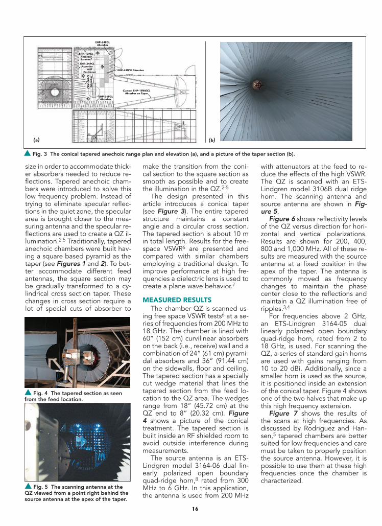
The design presented in this article introduces a conical taper (see Figure 3). The entire tapered structure maintains a constant angle and a circular cross section. The tapered section is about 10 m in total length. Results for the free-space VSWR6 are presented and compared with similar chambers employing a traditional design. To improve performance at high fre-quencies a dielectric lens is used to create a plane wave behavior.7
MEASURED RESULTSThe chamber QZ is scanned us-
ing free space VSWR tests6 at a se-ries of frequencies from 200 MHz to 18 GHz. The chamber is lined with 60” (152 cm) curvilinear absorbers on the back (i.e., receive) wall and a combination of 24” (61 cm) pyrami-dal absorbers and 36” (91.44 cm) on the sidewalls, floor and ceiling. The tapered section has a specially cut wedge material that lines the tapered section from the feed lo-cation to the QZ area. The wedges range from 18” (45.72 cm) at the QZ end to 8” (20.32 cm). Figure 4 shows a picture of the conical treatment. The tapered section is built inside an RF shielded room to avoid outside interference during measurements.
The source antenna is an ETS-Lindgren model 3164-06 dual lin-early polarized open boundary quad-ridge horn,8 rated from 300 MHz to 6 GHz. In this application, the antenna is used from 200 MHz
with attenuators at the feed to re-duce the effects of the high VSWR. The QZ is scanned with an ETS-Lindgren model 3106B dual ridge horn. The scanning antenna and source antenna are shown in Fig-ure 5.
Figure 6 shows reflectivity levels of the QZ versus direction for hori-zontal and vertical polarizations. Results are shown for 200, 400, 800 and 1,000 MHz. All of these re-sults are measured with the source antenna at a fixed position in the apex of the taper. The antenna is commonly moved as frequency changes to maintain the phase center close to the reflections and maintain a QZ illumination free of ripples.3,4
For frequencies above 2 GHz, an ETS-Lindgren 3164-05 dual linearly polarized open boundary quad-ridge horn, rated from 2 to 18 GHz, is used. For scanning the QZ, a series of standard gain horns are used with gains ranging from 10 to 20 dBi. Additionally, since a smaller horn is used as the source, it is positioned inside an extension of the conical taper. Figure 4 shows one of the two halves that make up this high frequency extension.
Figure 7 shows the results of the scans at high frequencies. As discussed by Rodriguez and Han-sen,5 tapered chambers are better suited for low frequencies and care must be taken to properly position the source antenna. However, it is possible to use them at these high frequencies once the chamber is characterized.
s Fig. 3 The conical tapered anechoic range plan and elevation (a), and a picture of the taper section (b).
Custom EHP-18WGCLAbsorber on Taper
EHP-24WW Absorber
(a) (b)
EHP-24PCLAbsorber
CR
V-6
0PC
LA
bsor
ber
EHP-36PCLAbsorber
AUTPositioner
EHP-24PCLAbsorber
A
B
C
D
EHP-12PCLAbsorberScanner
s Fig. 4 The tapered section as seen from the feed location.
s Fig. 5 The scanning antenna at the QZ viewed from a point right behind the source antenna at the apex of the taper.

17
COMPARISON WITH TRADITIONAL CHAMBERS
Comparison with traditional chambers is difficult. There are no two identical chambers that have the exact same absorber treatment with the exception of the taper geom-etry. A qualitative comparison, how-ever, suggests some advantages. With traditional chambers, anten-nas with gains of 16 dBi and above are required to achieve adequate illumination in the QZ. It appears that one of the features of the coni-cal taper is that lower gain antennas can be used. At 10 GHz, the source antenna has a directivity of 12 dBi,8 whereas the conical quad ridge horn used in many traditional tapered anechoic cham-bers has a directiv-ity of 14 dBi. The open boundary ridge horn is suc-cessfully used in the conical cham-ber design; how-ever, when used in a traditional cham-ber, a smooth am-plitude taper is not achieved (see Fig-ure 8).
In Figure 9, a comparison of the reflectivity of the conical tapered chamber and a tra-ditionally imple-mented chamber at 400 MHz shows a slight difference in back wall re-flectivity (180°), but this is related to differences in absorber treat-ment between the chambers. For the traditional cham-ber, one can see a large variation in reflectivity for the horizontal po-larization as the direction changes from 15° to 60° on
either side of the source antenna. These variations are not seen in the conical tapered chamber.
The chamber is configured with two ranges, a far field tapered range and a NF-FF planar and spherical range. Figure 3 shows the plan of the chamber with the two ranges. The antenna under test uses the same positioner for both ranges, and the QZ is the same as well. For the spherical range the probe is lo-cated between the QZ and the pla-nar scanner on the opposite wall. The planar scanner can be used for
s Fig. 6 Reflectivity results for the coni-cal tapered chamber at 200 (a), 400 (b), 800 MHz (c) and 1 GHz (d).
800 MHz Horizontal 800 MHz Vertical–39 dB limit
270
225
90
315
225 315
0180
135
(a)
(b)
(c)
(d)
45
270
270
270
90
90
90
225 315
225 315
0180
0180
0180
135 45
135 45
135 45
Measured Reflectivity Data
Measured Reflectivity Data
Measured Reflectivity Data
Measured Reflectivity Data
200 MHz Horizontal 200 MHz Vertical–30 dB limit
400 MHz Horizontal 400 MHz Vertical–36 dB limit
1,000 MHz Horizontal 1,000 MHz Vertical–42 dB limit
–35–40–45–50–55–60
–35–40–45–50–55–60
–35–40–45–50–55–60
–35–40–45–50–55–60
s Fig. 7 Reflectivity levels in the QZ versus angle at 2 (a), 4 (b), 10 (c), and 18 GHz (d).
270
225 315
135
(a)
(c)
(b)
(d)
45
90
270
225 315
135 45
90
180 1800
270
225 315
135 45
90
180 0
0
270
225 315
135 45
90
180 0
–40–50–60–70–80
–40–50–60–70–80
–40–50–60–70–80
–40–50–60–70–80
18,000 MHz Horizontal18,000 MHz Vertical–42 dB limit
Measured Reflectivity Data Measured Reflectivity Data
Measured Reflectivity Data Measured Reflectivity Data
2,000 MHz Horizontal2,000 MHz Vertical–42 dB limit
10,000 MHz Horizontal10,000 MHz Vertical–42 dB limit
4,000 MHz Horizontal4,000 MHz Vertical–42 dB limit
s Fig. 8 Data for a transverse scan of a traditional chamber using the same horn used in the conical design.
VBH 1 kHz Span 0 HzSweep 20.3 s (3000 pts)
Ref –34 dBmPeakLog5 dB/
W1 V2V3 FS
AA
The different curves are frommoving the antenna back and forthin the feed section trying to “tune”the best position
Atten 0 dB
5 dB/div
Center 10 GHzRes BW 1 kHz
18
The variables are defined in Fig-ure 11.
Given its size (2 m), the RF lens cannot be manufactured with tra-ditional dielectric materials due to the difficulty of controlling permit-tivity throughout the lens to a high degree of accuracy. Furthermore, it would be extremely heavy (∼1,000 kg), making installation difficult and requiring a special support struc-ture, potentially causing undesir-able diffractions.
To overcome these issues, a new low-loss, lightweight metamaterial
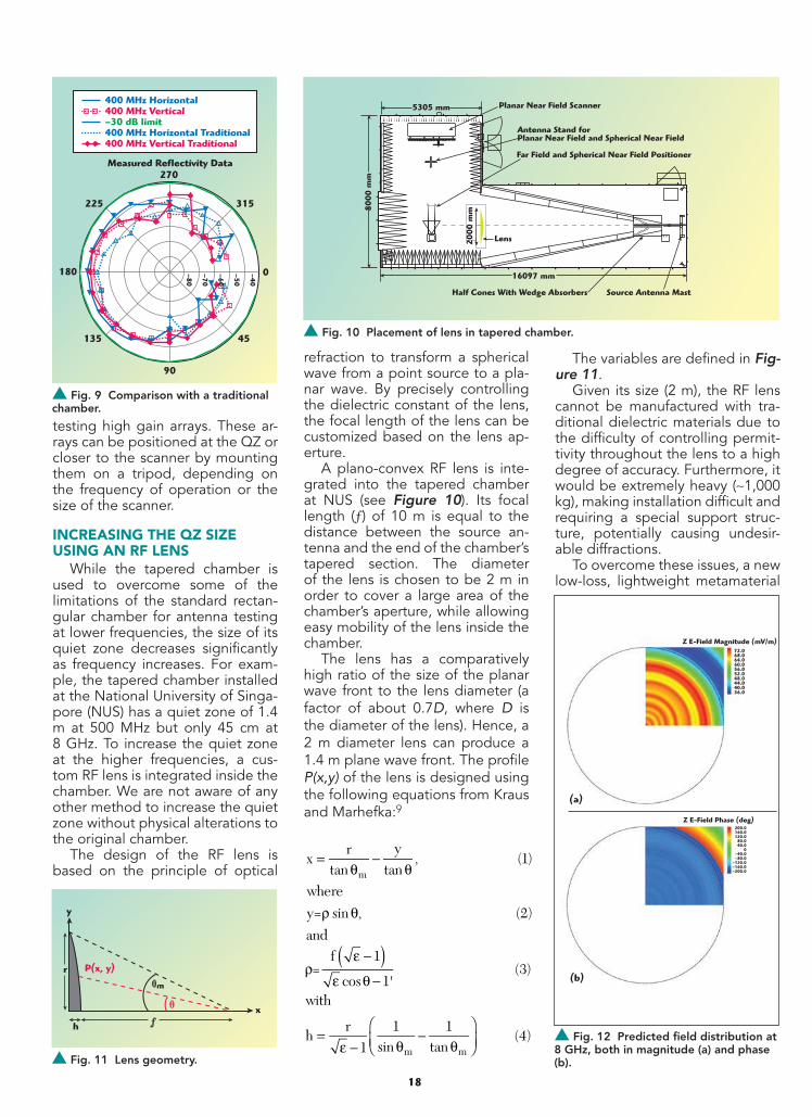
refraction to transform a spherical wave from a point source to a pla-nar wave. By precisely controlling the dielectric constant of the lens, the focal length of the lens can be customized based on the lens ap-erture.
A plano-convex RF lens is inte-grated into the tapered chamber at NUS (see Figure 10). Its focal length (ƒ) of 10 m is equal to the distance between the source an-tenna and the end of the chamber’s tapered section. The diameter of the lens is chosen to be 2 m in order to cover a large area of the chamber’s aperture, while allowing easy mobility of the lens inside the chamber.
The lens has a comparatively high ratio of the size of the planar wave front to the lens diameter (a factor of about 0.7D, where D is the diameter of the lens). Hence, a 2 m diameter lens can produce a 1.4 m plane wave front. The profile P(x,y) of the lens is designed using the following equations from Kraus and Marhefka:9
xr
tany
tan, (1)
where
y= sin , (2)
and
=f 1
cos 1'(3)
with
hr
11
sin1
tan(4)
m
m m
( )
=θ
−θ
ρ θ
ρε −
ε θ −
=ε − θ
−θ
⎛⎝⎜
⎞⎠⎟
xr
tany
tan, (1)
where
y= sin , (2)
and
=f 1
cos 1'(3)
with
hr
11
sin1
tan(4)
m
m m
( )
=θ
−θ
ρ θ
ρε −
ε θ −
=ε − θ
−θ
⎛⎝⎜
⎞⎠⎟
testing high gain arrays. These ar-rays can be positioned at the QZ or closer to the scanner by mounting them on a tripod, depending on the frequency of operation or the size of the scanner.
INCREASING THE QZ SIZE USING AN RF LENS
While the tapered chamber is used to overcome some of the limitations of the standard rectan-gular chamber for antenna testing at lower frequencies, the size of its quiet zone decreases significantly as frequency increases. For exam-ple, the tapered chamber installed at the National University of Singa-pore (NUS) has a quiet zone of 1.4 m at 500 MHz but only 45 cm at 8 GHz. To increase the quiet zone at the higher frequencies, a cus-tom RF lens is integrated inside the chamber. We are not aware of any other method to increase the quiet zone without physical alterations to the original chamber.
The design of the RF lens is based on the principle of optical
s Fig. 9 Comparison with a traditional chamber.
270
225 315
135 45
90
180 0–40
–50
–60
–70
–80
Measured Reflectivity Data
400 MHz Horizontal400 MHz Vertical–30 dB limit400 MHz Horizontal Traditional400 MHz Vertical Traditional
–40
–50
–60
–70
–80
s Fig. 10 Placement of lens in tapered chamber.
Planar Near Field Scanner
Half Cones With Wedge Absorbers
Lens
8000
mm
2000
mm
16097 mm
5305 mm
Source Antenna Mast
Antenna Stand forPlanar Near Field and Spherical Near Field
Far Field and Spherical Near Field Positioner
s Fig. 11 Lens geometry.
P(x, y)
x
r
y
h
�
�m
s Fig. 12 Predicted field distribution at 8 GHz, both in magnitude (a) and phase (b).
Z E-Field Magnitude (mV/m)
(a)
(b)
72.068.064.060.056.052.048.044.040.036.0
Z E-Field Phase (deg)200.0160.0120.0
80.040.0
0–40.0–80.0
–120.0–160.0–200.0

(corresponding to the quiet zone region) on the other side of the lens. For simplicity, the lens and the dipole are simulated in free-space without the tapered chamber since the primary aim of the simulation is to ensure that for the given length of the taper, the lens provides the best possible illumination. Includ-ing the chamber with its absorb-ers in the simulation model would drastically increase the problem size and complexity beyond the ca-pability of the numerical package at these high frequencies.
Figure 12 shows the predicted fields (for a quadrant) at 8 GHz. The circles in the plots represent the outline of the 2 m lens. Cuts of the fields along the lens diameter are shown in Figures 13 and 14 for 2 and 8 GHz, respectively. The fields of the dipole in the absence of the lens are superimposed in the figures for reference. For ease of comparison, the magnitudes are normalized to their respective mean values – the phase without the lens is normalized to its peak value and the phase with the lens is normalized to its mean value. From these figures, it is observed that the field with the lens deviates slightly from the dipole field due mainly to diffraction from the lens. However, the lens significantly reduces the large phase variation of the dipole field, producing a reasonably good plane wave in the vicinity of the quiet zone of the tapered chamber.
MEASURED PERFORMANCEThe lens is installed at the ap-
erture of the tapered chamber as shown in Figure 15 using a spe-cial frame made from low reflec-tion material to easily place and hold it. For the field measurement of the quiet zone, a simple linear scanner is set up as shown in Fig-ure 16. A broadband dual-ridged horn is used as the probe antenna. The field is measured along an axis transverse to the lens axis at about 2 m separation. The lens is then removed and the measurement repeated.
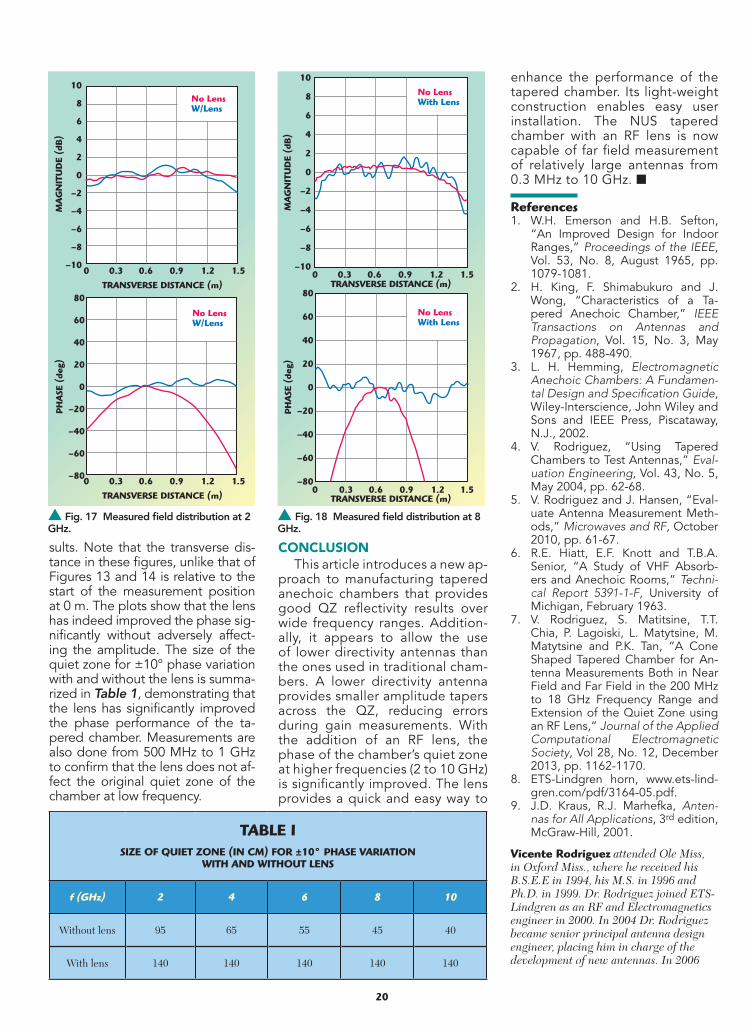
The results at 2 and 8 GHz are shown in Figures 17 and 18, re-spectively. The magnitudes and phases are “normalized” in the same manner as the numerical re-
manufactured by Matsing Pte Ltd. is used. The material allows the control of the dielectric permittiv-ity to a high degree of accuracy. It has extremely low-loss (ε’ < 10-4). Its low density (40 kg/m3) means that the 2 m lens weighs only 35 kg, making it portable and easily installed. The material is also iso-tropic and broadband, making the lens suitable for both vertical and horizontal polarizations over a wide range of frequencies.
NUMERICAL ANALYSISThe performance of the lens is
first evaluated using FEKO EM sim-ulation software. A half-wavelength dipole is placed at the focal length of the 2 m lens. The focal length corresponds to the distance (10 m) between the feed and aperture of the tapered chamber. The field is observed at a vertical plane at 2 m
19
s Fig. 13 Computed field distribution at 2 GHz.
10
8
6
4
2
0
–2
–4
–6
–8
–10
80
60
40
20
0
–20
–40
–60
–80
10.50–0.5–1
TRANSVERSE DISTANCE (m)
10.50–0.5–1
TRANSVERSE DISTANCE (m)
MA
GN
ITU
DE
(dB
)P
HA
SE (
deg)
No LensWith Lens
No LensWith Lens
s Fig. 14 Computed field distribution at 8 GHz.
10
8
6
4
2
0
–2
–4
–6
–8
–10
80
60
40
20
0
–20
–40
–60
–80
10.50–0.5–1
TRANSVERSE DISTANCE (m)
10.50–0.5–1
TRANSVERSE DISTANCE (m)
MA
GN
ITU
DE
(dB
)P
HA
SE (
deg)
No LensWith Lens
No LensWith Lens
s Fig. 15 View of the lens from the source antenna.
s Fig. 16 The QZ scanned with the lens in place at the end of the taper section.
20
CONCLUSIONThis article introduces a new ap-
proach to manufacturing tapered anechoic chambers that provides good QZ reflectivity results over wide frequency ranges. Addition-ally, it appears to allow the use of lower directivity antennas than the ones used in traditional cham-bers. A lower directivity antenna provides smaller amplitude tapers across the QZ, reducing errors during gain measurements. With the addition of an RF lens, the phase of the chamber’s quiet zone at higher frequencies (2 to 10 GHz) is significantly improved. The lens provides a quick and easy way to
sults. Note that the transverse dis-tance in these figures, unlike that of Figures 13 and 14 is relative to the start of the measurement position at 0 m. The plots show that the lens has indeed improved the phase sig-nificantly without adversely affect-ing the amplitude. The size of the quiet zone for ±10° phase variation with and without the lens is summa-rized in Table 1, demonstrating that the lens has significantly improved the phase performance of the ta-pered chamber. Measurements are also done from 500 MHz to 1 GHz to confirm that the lens does not af-fect the original quiet zone of the chamber at low frequency.
enhance the performance of the tapered chamber. Its light-weight construction enables easy user installation. The NUS tapered chamber with an RF lens is now capable of far field measurement of relatively large antennas from 0.3 MHz to 10 GHz. ■
References1. W.H. Emerson and H.B. Sefton,
“An Improved Design for Indoor Ranges,” Proceedings of the IEEE, Vol. 53, No. 8, August 1965, pp. 1079-1081.
2. H. King, F. Shimabukuro and J. Wong, “Characteristics of a Ta-pered Anechoic Chamber,” IEEE Transactions on Antennas and Propagation, Vol. 15, No. 3, May 1967, pp. 488-490.
3. L. H. Hemming, Electromagnetic Anechoic Chambers: A Fundamen-tal Design and Specification Guide, Wiley-Interscience, John Wiley and Sons and IEEE Press, Piscataway, N.J., 2002.
4. V. Rodriguez, “Using Tapered Chambers to Test Antennas,” Eval-uation Engineering, Vol. 43, No. 5, May 2004, pp. 62-68.
5. V. Rodriguez and J. Hansen, “Eval-uate Antenna Measurement Meth-ods,” Microwaves and RF, October 2010, pp. 61-67.
6. R.E. Hiatt, E.F. Knott and T.B.A. Senior, “A Study of VHF Absorb-ers and Anechoic Rooms,” Techni-cal Report 5391-1-F, University of Michigan, February 1963.
7. V. Rodriguez, S. Matitsine, T.T. Chia, P. Lagoiski, L. Matytsine, M. Matytsine and P.K. Tan, “A Cone Shaped Tapered Chamber for An-tenna Measurements Both in Near Field and Far Field in the 200 MHz to 18 GHz Frequency Range and Extension of the Quiet Zone using an RF Lens,” Journal of the Applied Computational Electromagnetic Society, Vol 28, No. 12, December 2013, pp. 1162-1170.
8. ETS-Lindgren horn, www.ets-lind-gren.com/pdf/3164-05.pdf.
9. J.D. Kraus, R.J. Marhefka, Anten-nas for All Applications, 3rd edition, McGraw-Hill, 2001.
Vicente Rodriguez attended Ole Miss, in Oxford Miss., where he received his B.S.E.E in 1994, his M.S. in 1996 and Ph.D. in 1999. Dr. Rodriguez joined ETS-Lindgren as an RF and Electromagnetics engineer in 2000. In 2004 Dr. Rodriguez became senior principal antenna design engineer, placing him in charge of the development of new antennas. In 2006
s Fig. 17 Measured field distribution at 2 GHz.
10
8
6
4
2
0
–2
–4
–6
–8
–10
80
60
40
20
0
–20
–40
–60
–80
1.51.20.90.60.30
TRANSVERSE DISTANCE (m)
1.51.20.90.60.30
TRANSVERSE DISTANCE (m)
MA
GN
ITU
DE
(dB
)P
HA
SE (
deg)
No LensW/Lens
No LensW/Lens
10
8
6
4
2
0
–2
–4
–6
–8
–10
80
60
40
20
0
–20
–40
–60
–80
1.51.20.90.60.30TRANSVERSE DISTANCE (m)
1.51.20.90.60.30TRANSVERSE DISTANCE (m)
MA
GN
ITU
DE
(dB
)P
HA
SE (
deg)
No LensWith Lens
No LensWith Lens
s Fig. 18 Measured field distribution at 8 GHz.
TABLE ISIZE OF QUIET ZONE (IN CM) FOR ±10° PHASE VARIATION
WITH AND WITHOUT LENS
f (GHz) 2 4 6 8 10
Without lens 95 65 55 45 40
With lens 140 140 140 140 140

21
position of engineer at Matsing Pte. Ltd. His research interests include antenna measurement system and RF lenses.
Leo Matytsine received his B.S. from the University of Southern California in 2009 and his MBA from the Australian Global School of Management in 2013. He has been with Matsing Pte. Ltd. since 2009 and currently holds the position of director. His interests include RF convex lenses and antenna measurement systems.
Michael Matytsine received his B.A. from Chapman University in 2006 and his MBA from La Verne University in 2010. He has been with Matsing Pte. Ltd. since 2006 and currently holds the position of director. His interests include Luneburg and convex RF lenses.
Peng-Khiang Tan received his degree in electronic and computer engineering from Ngee Ann Polytechnic in 1999 and his Bachelor of Technology in Electronics Engineering (second Class Honors) from the National University of Singapore in 2008. He currently works as a laboratory technologist within the antenna group at the Temasek Laboratories of the National University of Singapore.
and technical director of Matsing Pte. Ltd. His research interests include electromagnetic materials, metamaterials, smart materials, multi-beam antennas, antenna measurement techniques, and most recently, lightweight, large-size RF lenses. He has more than 60 publications in these areas, as well as four patents.
Tse-Tong Chia received his B.Eng. degree with first class honors in 1986 from the National University of Singapore, and his M.S. and Ph.D. in 1991 and 1994, respectively, from Ohio State University. He has been with the DSO National Laboratories in Singapore since 1986, where he is currently a distinguished member of the technical staff. Chia was a laboratory head from 1995 until 2010 when he stepped down to focus on research. He is currently also a principal research scientist in the Temasek Laboratories at the National University of Singapore. His research interests include computational methods for electromagnetic scattering and installed antenna performance, as well as the use of lenses for antenna applications.
Pavel Lagoiski received his B.S. E.E. from the National University of Singapore in 2010. Since then he has held the
Dr. Rodriguez became antenna product manager, placing him in charge of development, marketing and maintenance of the antenna product line. Dr. Rodriguez is the author of more than 50 publications and holds patents for hybrid absorber and dual ridge horn antennas.
Serguei Matitsine graduated with honors from the Moscow Institute of Physics and Technology in 1979 and received his Ph.D. in 1982. From 1982-1984 he held the position of senior researcher at the Institute of Radio-Engineering and Electronics of the Russian Academy of Sciences. From 1984 until 1995 he has held several positions including senior researcher, head of the electromagnetic laboratory and deputy director at the Institute of Theoretical and Applied Electromagnetics of Russian Academy of Sciences. In 1995 Dr. Matitsine joined the research and development group at Singapore Technologies Aerospace as technical director and later moved to the position of chief engineer. Since 2001 Dr. Matitsine has also been working at Temasek Laboratories of the National University of Singapore as an adjunct senior principal research scientist. He is also the chairman
CobaltFxVNAFrequencyExtensionSystemwithbandsfrom50GHzto110GHz
Thecost-effectivemillimeterwavefrequencyextensionsystem,CobaltFx,isaninnovativeapproachformillimeter-waveS-parametermea-surementsofferingindustryleadingdynamicrangeandsweepspeeds.Thesystemcanbeusedforavarietyofantennaapplicationsinclud-ingwaveguidecapablepositionersperforminglivebasicantennaandRCSmeasurements.The
frequencyextenders’dedicatedwaveguidebandsof50-75GHz,60-90GHzand75-110GHzcanbeanchoredbyyourchoiceoffourVNAs.The2-portC4209and4-portC4409are9GHzVNAswithadynamicrangeof152dBtyp.(10HzIFBW).The2-portC4220and4-portC4420coverupto20GHzandofferadynamicrangeof135dBtyp.(10HzIFBW).CobaltFxsystemincludesextensionmodulesfromFarranTechnologypairedwithaCopperMountainTechnologyCobaltUSBvectornetworkanalyzerandallnecessarycables,adaptersandaprecisioncalibrationkit.http://www.coppermountaintech.com/products/Ohm-50/category/16/

Characterizing and Tuning Antennas Using an Automated Measurement System and a VNACopper Mountain TechnologiesIndianapolis, Ind.Diamond EngineeringDiamond Springs, CA
APPLICATION PROFILEAs the number of devices featuring wire-
less connectivity grows, ensuring their per-formance specifications while staying with-in regulatory requirements becomes even more important. Antenna pattern measure-ment is a critical step in the design process of antennas and wireless devices. Compact antenna measurement systems combined with a high performance VNA are necessary to characterize parameters such as pattern, gain, VSWR, and efficiency. These results are used to validate simulated designs and identify possible performance issues before final testing. By using an in-house measure-ment system, multiple design revisions can be tested and pre-certified without the
high cost of using an accredited or certified measurement facility for each test. Other considerations like portability and low cost are important to engineers in various en-vironments like defense or education, re-spectively.
CHALLENGESMaking accurate antenna measurements
carries a number of challenges, some of the most important being dynamic range, calibration, and speed. A sufficient dynamic range will allow the antenna to be measured accurately at both minimum and maximum signal level with a minimal amount of trace noise. Older network analyzers can reach a reasonable dynamic range and reduced noise by reducing the IF bandwidth but the analyzer speed is greatly reduced, a single sweep can take many seconds to complete. PC-based VNA’s offer the benefit of greater initial dynamic range, higher speeds, and direct data transfer.
22
Copper Mountain Technologies
Application Profile As the number of devices featuring wireless connectivity
grows, ensuring their performance specifications while staying within regulatory requirements becomes even more important. Antenna pattern measurement is a critical step in the design process of antennas and wireless devices. Compact antenna measurement systems combined with a high performance VNA are necessary to characterize parameters such as pattern, gain, VSWR, and efficiency. These results are used to validate simulated designs and identify possible performance issues before final testing. By using an in-house measurement system, multiple design revisions can be tested and pre-certified without the high cost of using an accredited or certified measurement facility for each test. Other considerations like portability and low cost are important to engineers in various environments like defense or education, respectively.
ChallengesMaking accurate antenna measurements carries a number
of challenges, some of the most important being dynamic range, calibration, and speed. A sufficient dynamic range will allow the antenna to be measured accurately at both minimum and maximum signal level with a minimal amount of trace noise. Older network analyzers can reach a reasonable dynamic range and reduced noise by reducing the IF bandwidth but the analyzer speed is greatly reduced, a single sweep can take many seconds to complete. PC-based VNA’s offer the benefit of greater initial dynamic range, higher speeds, and direct data transfer.
Application: Characterizing the AntennaIn this example, an unknown 2.4 GHz antenna is
characterized, with a configuration consisting of: Diamond Engineering DAMS 5000 positioner with an FSM spherical mount, RF cables, a calibrated reference antenna, a Copper Mountain Technologies Planar 804/1 VNA, and a computer (PC) running the measurement and VNA software. To begin, the VNA is set to the antenna's frequency range, all RF cable loss (including positioner) is calibrated out using the VNA’s built in 12 term calibration. Once the calibration is complete the AUT is mounted to the positioner’s RF Rotary Joint and the reference antenna is connected then positioned at the appropriate distance (typically 1 or 3 meters). Now that the antennas are connected and the VNA is set to transmission (S
12 or S
21), the
VNA will show the response of the entire link. At this point the user can note the signal response on the analyzer; if the polarization is correct and the AUT is at a point of high signal,
the VNA should show a strong profile with little trace noise. Depending on the type of antenna being measured, the antenna can be manually positioned
to a point of lowest signal to confirm that the signal is still above the noise floor and the trace noise is acceptable for testing requirements. After the setup is verified, the DAMS antenna measurement software is used to make a measurement. The software indexes the antenna to every physical point and executes a transmission sweep on the VNA. Optionally, VSWR data can be automatically collected at every point. Once complete, the entire data set can be viewed,
processed and exported.
Characterizing and Tuning Antennas Using an
Automated Measurement System and a VNAAPP NOTE
Precision RF Cables
The full DAMS setup
Scalar or Vector* Calibration(* Requires VNA)
DAMS Positioner / AUT
Controller
DAMS Antenna Measurement Studio
USBGPIB / Ethernet / USB
VNA, Rec. Only or Source/Receiver

23
unwanted environment reflections, the VNA can be switched to S21 Time Domain mode. Reflections outside of the direct path will show up as unusually large spikes indi-cating that the signal is being re-flected. The absorber can now be placed to block the unwanted re-flections. After changes have been made to the antenna and/or the test setup, another measurement can be made quickly to verify and record these changes. The end re-sult is a refined antenna design with accurate, publishable test data.
INCORPORATING A PC-BASED VNA
Several specific features and modes of the analyzer were key in this application, including transmis-sion, reflection, VSWR, dynamic range, Time Domain, and sweep speed. All of these are crucial for the measurement and design of antennas and related systems. Antenna measurements contain a large amount of data: a single polarization full spherical measure-ment using 10 degree resolution and 51 frequencies contains over 33,000 data points. The ability to automate these measurements us-ing the Planar 804/1 VNA scripts and DAMS 5000 positioner saved many hours compared to manu-al testing. In this application the VNA’s high measurement speed of 100 μs enabled real-time tuning and fast data collection.
or S21), the VNA will show the re-sponse of the entire link. At this point the user can note the signal response on the analyzer; if the po-larization is correct and the AUT is at a point of high signal, the VNA should show a strong profile with little trace noise. Depending on the type of antenna being measured, the antenna can be manually posi-tioned to a point of lowest signal to confirm that the signal is still above the noise floor and the trace noise is acceptable for testing require-ments. After the setup is verified, the DAMS antenna measurement software is used to make a mea-surement. The software indexes the antenna to every physical point and executes a transmission sweep on the VNA. Optionally, VSWR data can be automatically collected at every point. Once complete, the entire data set can be viewed, pro-cessed and exported.
POST-MEASUREMENT ANALYSIS AND TUNING
Analyzing the measurement data may reveal certain problems such as low gain, pattern distor-tion, or frequency response issues. Since the Planar 804/1 VNA is still fully calibrated it can be used to tune and troubleshoot the antenna in real time. For live antenna tun-ing, the analyzer is switched to S22 mode, and the user can make small modifications to the antenna while seeing the results immediately dis-played. To identify multi-path and
APPLICATION: CHARACTERIZING THE ANTENNA
In this example, an unknown 2.4 GHz antenna is characterized, with a configuration consisting of: Diamond Engineering DAMS 5000 positioner with an FSM spherical mount, RF cables, a calibrated ref-erence antenna, a Copper Moun-tain Technologies Planar 804/1 VNA, and a computer (PC) running the measurement and VNA soft-ware. To begin, the VNA is set to the antenna’s frequency range, all RF cable loss (including positioner) is calibrated out using the VNA’s built in 12 term calibration. Once the calibration is complete the AUT is mounted to the positioner’s RF Rotary Joint and the reference antenna is connected then posi-tioned at the appropriate distance (typically 1 or 3 meters). Now that the antennas are connected and the VNA is set to transmission (S12
COPPER MOUNTAIN TECHNOLOGIES
US: +1.317.222.5400 | Asia: +65.63.23.6546
coppermountaintech.com
Post-Measurement Analysis and TuningAnalyzing the measurement data may reveal certain
problems such as low gain, pattern distortion, or frequency response issues. Since the Planar 804/1 VNA is still fully calibrated it can be used to tune and troubleshoot the antenna in real time. For live antenna tuning, the analyzer is switched to S
22 mode, and the user can make small modifications to the
antenna while seeing the results immediately displayed. To identify multi-path and unwanted environment reflections, the VNA can be switched to S
21 Time Domain mode. Reflections
outside of the direct path will show up as unusually large spikes indicating that the signal is being reflected. The absorber can now be placed to block the unwanted reflections. After changes have been made to the antenna and/or the test setup, another measurement can be made quickly to verify and record these changes. The end result is a refined antenna design with accurate, publishable test data.
Incorporating a PC-Based VNASeveral specific features and modes of the analyzer were
key in this application, including transmission, reflection, VSWR, dynamic range, Time Domain, and sweep speed. All of these are crucial for the measurement and design of antennas and related systems. Antenna measurements contain a large amount of data: a single polarization full spherical measurement using 10 degree resolution and 51 frequencies contains over 33,000 data points. The ability to automate these measurements using the Planar 804/1 VNA scripts and DAMS 5000 positioner saved many hours compared to manual testing. In this application the VNA’s high measurement speed of 100 µs enabled real-time tuning and fast data collection.
SummaryComplete antenna measurement and characterization can
be quickly achieved using a compact antenna measurement system powered by a PC-based VNA and the DAMS studio. Traditional pattern measurement systems often use a separate source and receiver, limiting measurements to either single frequency or stepped CW modes of operation. The test equipment for these systems is often dedicated and limited to just the measurement of the antenna without parameters such as phase and VSWR. The Planar 804/1 VNA contains all of the tools and capability required for the measurement, design, and tuning of the antenna. Fast, broadband vector based measurements with low noise and high dynamic range are essential for the wireless technology of today and tomorrow. Combining a compact antenna measurement system with the flexibility of an automation ready, PC-based VNA from Copper Mountain Technologies provides a low cost solution that greatly reduces development time and increases product performance.
Left: the AUT is tuned at 2420 MHzRight: the VNA and DAMS software
operate in tandem on a PC
The yellow trace shows S22
of the AUT after tuning
Left: the AUT is tuned at 2420 MHzRight: the VNA and DAMS software operate in tandem on a PC
COPPER MOUNTAIN TECHNOLOGIES
US: +1.317.222.5400 | Asia: +65.63.23.6546
coppermountaintech.com
Post-Measurement Analysis and TuningAnalyzing the measurement data may reveal certain
problems such as low gain, pattern distortion, or frequency response issues. Since the Planar 804/1 VNA is still fully calibrated it can be used to tune and troubleshoot the antenna in real time. For live antenna tuning, the analyzer is switched to S
22 mode, and the user can make small modifications to the
antenna while seeing the results immediately displayed. To identify multi-path and unwanted environment reflections, the VNA can be switched to S
21 Time Domain mode. Reflections
outside of the direct path will show up as unusually large spikes indicating that the signal is being reflected. The absorber can now be placed to block the unwanted reflections. After changes have been made to the antenna and/or the test setup, another measurement can be made quickly to verify and record these changes. The end result is a refined antenna design with accurate, publishable test data.
Incorporating a PC-Based VNASeveral specific features and modes of the analyzer were
key in this application, including transmission, reflection, VSWR, dynamic range, Time Domain, and sweep speed. All of these are crucial for the measurement and design of antennas and related systems. Antenna measurements contain a large amount of data: a single polarization full spherical measurement using 10 degree resolution and 51 frequencies contains over 33,000 data points. The ability to automate these measurements using the Planar 804/1 VNA scripts and DAMS 5000 positioner saved many hours compared to manual testing. In this application the VNA’s high measurement speed of 100 µs enabled real-time tuning and fast data collection.
SummaryComplete antenna measurement and characterization can
be quickly achieved using a compact antenna measurement system powered by a PC-based VNA and the DAMS studio. Traditional pattern measurement systems often use a separate source and receiver, limiting measurements to either single frequency or stepped CW modes of operation. The test equipment for these systems is often dedicated and limited to just the measurement of the antenna without parameters such as phase and VSWR. The Planar 804/1 VNA contains all of the tools and capability required for the measurement, design, and tuning of the antenna. Fast, broadband vector based measurements with low noise and high dynamic range are essential for the wireless technology of today and tomorrow. Combining a compact antenna measurement system with the flexibility of an automation ready, PC-based VNA from Copper Mountain Technologies provides a low cost solution that greatly reduces development time and increases product performance.
Left: the AUT is tuned at 2420 MHzRight: the VNA and DAMS software
operate in tandem on a PC
The yellow trace shows S22
of the AUT after tuningThe yellow trace shows S22 of the AUT after tuning

24
range are essential for the wireless technology of today and tomorrow. Combining a compact antenna measurement system with the flex-ibility of an automation ready, PC-based VNA from Copper Mountain Technologies provides a low cost solution that greatly reduces devel-opment time and increases prod-uct performance.
SUMMARYComplete antenna measure-
ment and characterization can be quickly achieved using a compact antenna measurement system pow-ered by a PC-based VNA and the DAMS studio. Traditional pattern measurement systems often use a separate source and receiver, limit-ing measurements to either single frequency or stepped CW modes
of operation. The test equipment for these systems is often dedicat-ed and limited to just the measure-ment of the antenna without pa-rameters such as phase and VSWR. The Planar 804/1 VNA contains all of the tools and capability required for the measurement, design, and tuning of the antenna. Fast, broad-band vector based measurements with low noise and high dynamic
2-and4-PortUSBVNAsfrom100kHzto20GHzCopperMountainTechnologies’CobaltSeriesUSBVNAs’industry-leadingdynamicrange,152*dBtyp.(10HzIFBW),andsweepspeed,10*µsmin.typ.,makethemidealforfastproductionanddiverseresearchapplications.2-and4-Portmodelswithoptionsfordirectreceiveraccessandfrequencyextension.*modelspecific.
http://www.coppermountaintech.com/products/Ohm-50/category/13/

25
Practical Antenna Connection for Accurate TestingClayton Karmel, Pdicta Corp, San Diego, CA and Ben Maxson, Copper Mountain, Indianapolis, Ind.
Connecting RF test and measurement equipment to an Antenna Under Test (AUT) usually involves tradeoffs
among measurement accuracy, electrical considerations, cost, and mechanical rug-gedness. In this article, we describe some aspects of this connection with practical
advice for such test and measurement sce-narios.
Tools of the Trade
TESTING VIA AN RF TEST CONNECTOR: U.FL VS COAXIAL SWITCH
When provided, an antenna test port will usually be at a 50 ohm point. If the design includes a coax switch for inspection
and final test purposes, an antenna test sample can be produced or reworked with the switch rotated 180°. This reverses the in and out terminals so con-necting a test cable inter-
rupts the feedline and the cable faces the antenna instead of the device.
A test port and test cable of the appro-priate type reduces the need for strain relief as the cable can be connected just before measuring. A right-angle connector at the device end may further reduce stress and allow easier routing through the device housing. Note that most ultra-miniature connectors have a mating life on the order of a few dozen cycles, but failure will be-come self-evident in the measurements.SMA to RF switch, SMA to U.FL (both sexes), SMB, SMA bullet and SMA
to U.FL short cable, and a Vector Network Analyzer.

26
The example PCB on the left has a U.FL connector on a very short stub. One can isolate the WiFi de-vice by omitting the 100pf cap and installing the U.FL to obtain coaxial access to the antenna. Alterna-tively, and as shown at right, an RF switch can be installed allowing for
testing either the WiFi module or the antenna.
CUSTOM CAL STANDARDSLumped element tuning for PCB
antennas requires that your VNA calibration is in the proximity of the next series or shunt element to be added. You have options:• Use a co-axial calibration stan-
dard, usually to an SMA inter-face, and then extend the ref-erence plane across the length of your board connection. This extension may compensate for an SMA-U.FL adaptor, or maybe a short cable. Add reference plane time until the ‘Open’ is
at the right edge of the Smith chart.
• Create a home-brew set of Cali-bration standards. Take three sparsely populated boards; add 50 Ohm shunt, 100pf shunt (short) and one left open.
• If the reference plane isn’t ex-tended by either custom calibra-tion standards or by manually extending the reference plane, then matching efforts will be ex-tremely confused because the Smith chart will be rotated. This test board omitted the
WiFi IC, installing a U.FL connec-tor, instead. We made four of these boards, one each configured for Load, Open, Short and Thru to the un-matched Antenna.
Now we can calibrate to the entry point of the antenna with the short, open and 50 ohm load. In production, there are no extra components or space required.
Alternatively, if we had used coaxial calibration standards (N or SMA), we would subsequently “ex-tend” the reference plane by an ad-justment in the VNA, usually called Port Extension. How far? Use the Open and Short configurations and extend the reference plane until these align with the right and left edges of the Smith Chart.
If your instrument and cabling mass is substantial compared to the counterpoise (ground-plane) of the board, add a DC-DC connec-tor prior to calibration. When you start to match, move the reference plane (Port Extension) backwards, bringing the reference plane back with you as you add tuning ele-ments.
TUNING A LOOPThe keyfob design below was
based on a radio chip with a dif-ferential output. The round shape of the board and differential drive suggested a loop antenna which is less susceptible to de-tuning than a monopole, dipole or folded F. Dielectric detuning happens when the keyfob is held by different hands or in different orientations or sits on different surfaces.
On the right is the production board with differential RF feed at the top of the image. On the left
An RF Switch allows production testing of the WiFi module. Turn it around to tune the antenna. But it adds cost to every unit.
U.FL connector sits on a stub with the same length as the trace to the WiFi module. In production, omit the U.FL connector.
Application-Specific RF test board

Open/Short/Load values in and out of place.
50 Ohm matches are increas-ingly typical at the output of mixed signal RF SOC IC’s, but if not, re-view your options at your duplexer, diplexer, balun or within your RF matching circuit to the antenna. The ideal test point has close by ac-cess to the antenna’s ground plane, preferably one well reinforced with vias.
Whether your coaxial cable at-tached with “horizontal” or “verti-cal” launch, the goal is to maintain the TEM modes that exist between the center conductor and shield of the test cable the feedline microstrip and its ground plane through the transition between them.
A 50 ohm microstrip feed line may be as little as 0.03 to 0.1 mm (.015” to .025”) wide if over an embedded ground plane of a thin circuit board assembly. Protect-ing such a thin trace from being pulled up by the test cable requires a mechanically sound connection between the cable sheath or shield and the ground plane, preferably in an area where the ground plane is reinforced by vias.
HORIZONTAL LAUNCHFor a horizontal launch, to the ex-
tent possible the test cable should access the broken microstrip feed-line trace directly from the ground plane and in the direction of the feedline. Keep the feed line and center conductor and their separate ground return currents close by, in proximity, parallel to each other, and minimally different in length. Avoid 90° connections and bends until both currents are safely within the test cable. Eisenhart’s “edge-launch design” can be approximat-ed even if the test point is not on the edge of the circuit board.
VERTICAL LAUNCHFor a vertical launch, it may be
practical to break the feedline trace and reflow solder a U.FL or simi-lar surface mount connector to the feedline at the break and the ground plane on both sides. This gives the ruggedness advantage of the con-nector, albeit at the presence of some reflection. If this isn’t practi-
in design, or maybe the product requirements were just too tight. Here are some coaxial cable op-tions if you need to forge a reliable transmission line connection.
First, you will most likely want to identify a position on your board where the impedance is, or is ex-pected to be, 50 ohms. This isn’t al-ways required, but simplifies things. Remember that you still face two calibration/reference plane options – calibrating with normal standards at the ‘connector’ end of your co-axial cable, then extending the ref-erence plane, or building multiple boards and implementing a cus-tom ‘calibration set’.
The latter option can be a prob-lem in this case, however, because it requires that your coaxial cable have the same electrical length on each of 3-4 boards, or that you have to regularly solder your
is a test board with the same an-tenna and same ground-plane. Notice tuning elements both at the entry of the differential drive and at the mid-way point. L5 enables the loop to be extended, in case simulations (or back-of-the-hand guesses) are off when judging loop size/characteristics.
Notice Y2. It’s a 1:1 balun, con-figured so that a single-ended RF interface can drive the loop dif-ferentially. Look up the radio IC’s component output match and tune the antenna impedance to the complex conjugate of that match. Remember to extend the reference plane to the lumped elements first.
TESTING WITHOUT A COAXIAL CONNECTOR
Sometimes there just isn’t an opportunity to have a U.Fl or Coax-ial switch. Maybe it was overlooked
Small board example RF Test Circuit
Small board example, loaded as Calibration ‘Load’
Small board example, loaded as Calibration ‘Short’
27

cal, the device doesn’t need to re-main functional, and ground plane is accessible on the other side of the circuit board assembly beneath the
feedline, the ap-proach below may work. A clearance hole is drilled for the test cable di-electric, which is trimmed to the board thickness, and the emerging center conductor soldered closely to the feed trace at the break. The shield should be tightly flared so as to be soldered closely to the ground plane beneath.
USING A BALUNA further refine-
ment might help exclude the test
cable from the measurement if the DUT has insufficient ground plane and common mode currents on
the cable result. This can be done by forming a 1-turn loop around the minimum bending radius for a semi-flexible or hand-formable test cable, or with a ferrite bead or two placed over the test cable where it departs from the ground plane. While ferrite beads are not characterized above 500 MHz and all of them lose performance as frequency increases, they are in-expensive and unlikely to impair the test results. Type 61 ferrites are usually recommended above 300 MHz but Type 43 is available in a greater range of dimensions and may work.
A bead can be selected for fit and evaluated by placing a sample at the shorted end of a coax stub and extending the R54 port to that point. As a useful example, the Kemet B-20L-44 RG-178 stub dem-onstrated |Z| in excess of 58 ohms out to 3 GHz, which includes the GSM, UMTS, and LTE to Band 7. It was in excess of 30 ohms out to 5GHz. Any common mode current from the DUT can be arbitrarily re-duced by stacking multiple beads.
CABLE LENGTH AND TYPERegarding the choice off cable,
here are some points to consider:• Test Cable: The test cable
should be long enough to place the test instrument out of the near field of the AUT and pref-erably a few wavelengths away. This reduces reflections off the test instrument itself so the an-tenna measurement will better approach the limits of the test environment.
• Test Cable Type: The thinner and more flexible the cable, the less strain relief required for rug-gedness under test; on the oth-er hand, the thinner the cable, the greater the attenuation loss which limits the measurement accuracy. To follow is a table of cable types typically available in commercial cable assemblies. If the required test cable length
introduces significant loss, it may be possible to include the coaxial adaptors and test cable in the in-strument calibration using a tightly constructed short, open, and a 50 Ohm chip resistor on a brassboard
RF test and production board with Loop Antenna.
Small board example, Measuring the Antenna raw match with extended reference plane.
Small board example, loaded as Calibration ‘Open’
28
Test circuit for Loop antenna.

of similar construction to the DUT.
CONCLUSIONThe typical integral antenna in
the 2.4GHz ISM bands and up is a compromise to begin with because
of multiple band requirements and size and space constraints; accord-ingly, the typical SWR may be far more significant than reflection or attenuation from a less than ideal
test cable interface. Every device will be different, but keeping the TEM modes in mind in making the test connection won’t hurt and will make for the most accurate test.
Solder to Ground Plane
Break Feedline
EisenhartEdge Launch
Matching Network
Chip or Other Ant
Braid Avoid 90°Connectionif possible
Test Cable
OK to Bend
2929
Clearance Hole
Dielectric
Sharp Flare in Braid

30
Compact2-PortUSBVNAsupto8.5GHzFrequencyCopperMountainTechnologies’popularCom-pactSeriesdeliversfull-featuredlab-gradeperformanceinacompactpackagesuitableformanyresearchandproductionapplica-tions.Theseinstrumentsareagreatvalue
solutionformagnitudeandphasemeasurementsfrom9kHzto8.5GHzandanoptionfor75Ωmeasurementsto3GHz.http://www.coppermountaintech.com/products/Ohm-50/category/11/

COST-EFFECTIVE MM-WAVE SYSTEMCobaltFx Frequency Extension System is an unprecedented approach for millimeter-wave S-parameter measurements, suited for antenna range measurements, automotive radar & sensor testing, material characterization, and many other mm-Wave applications.
The system is anchored by a Cobalt Series USB VNA
Includes frequency extension modules and all necessary accessories in collaboration with Farran Technology
www.coppermountaintech.com
Read the white paper from Frost & Sullivan about the high-performance Millimeter Wave VNA System: http://cpmt.link/fswhitepaper
EXTEND YOUR REACHDiamond Engineering has integrated the CobaltFx Frequency Extension System into their antenna measurement system.
In collaboration with:
www.farran.com
C4209 Available options are 2- and
4-port VNAs with a maximum frequency of 9 GHz or 20 GHz
Three dedicated waveguide bands, 50-75 GHz, 60-90
GHz and 75-110 GHz
Visit the websites below for more information on the
CobaltFx System: cpmt.link/cobaltfx or
cpmt.link/farrancobaltfx