present and future packaging solutions for the mobile ... · on-chip integration not ideal for...
TRANSCRIPT

Present and Future
Packaging Solutions for
the Mobile & IoT Industry
JEDEC Mobile & IOT Forum Copyright © 2016
Nantong Fujitsu Microelectronics Co., Ltd.1
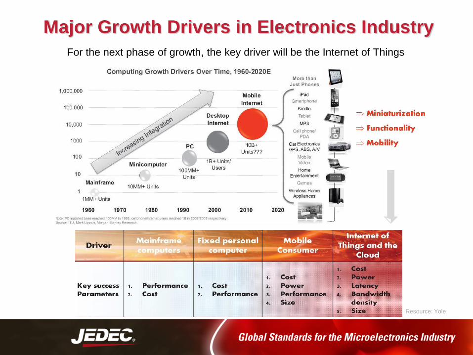
Major Growth Drivers in Electronics Industry
Resource: Yole
For the next phase of growth, the key driver will be the Internet of Things

What is IoT / IoE
IoT will connect everything with everyone to form a global integrated network
IoT is driven by integration of multiple technologies in combination with lower
costs
IoT will enhance “things”, “objects” or “machines” with embedded computing
and ubiquitous communication technologies
IoT device typically consists of Sensors/actuators, embedded microcontrollers
and connectivity hardware
Receiving
• MEMS/Sensors
• Actuators
Computing
• Microcontrollers
• Data analytics
• Memories
• Cloud platforms
Communication
• Wireless
communication
• Wired
communication
Source: ST
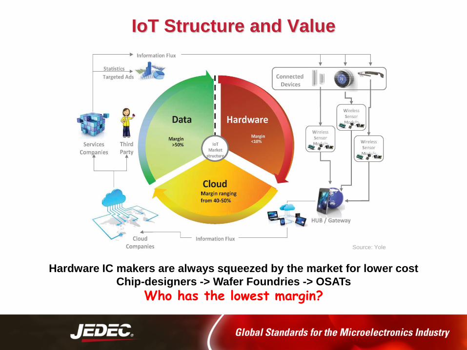
IoT Structure and Value
Source: Yole
Hardware IC makers are always squeezed by the market for lower cost
Chip-designers -> Wafer Foundries -> OSATs
Who has the lowest margin?

Basic Building Blocks for IoT
Key technologies:• Sensing
• Processing
• Connectivity
Supported by:• Sensor/machine infrastructure
• Communication backbone
• M2M service layer
• Application platform
MCUCPU/Memory/I/O
MEMS
SensorInput/OutputInput
WiFi
BT
GPS
Display

Source: IEEE
All devices—limited only by our imagination—will form a “close loop control” via
sensors, and MCUs with the world through a wireless network.
IoT Making Objects Smart
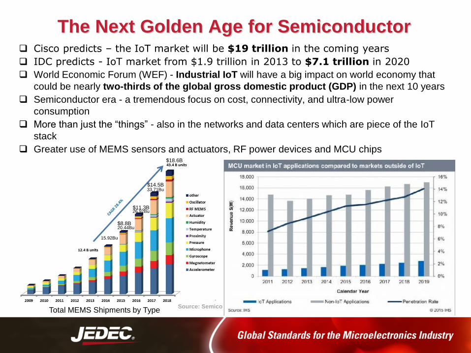
The Next Golden Age for Semiconductor Cisco predicts – the IoT market will be $19 trillion in the coming years
IDC predicts - IoT market from $1.9 trillion in 2013 to $7.1 trillion in 2020
World Economic Forum (WEF) - Industrial IoT will have a big impact on world economy that
could be nearly two-thirds of the global gross domestic product (GDP) in the next 10 years
Semiconductor era - a tremendous focus on cost, connectivity, and ultra-low power
consumption
More than just the “things” - also in the networks and data centers which are piece of the IoT
stack
Greater use of MEMS sensors and actuators, RF power devices and MCU chips
Total MEMS Shipments by TypeSource: Semico
$8.8B
$11.3B
$14.5B
$18.6B
15.92Bu
20.44Bu
26.92Bu
33.71Bu
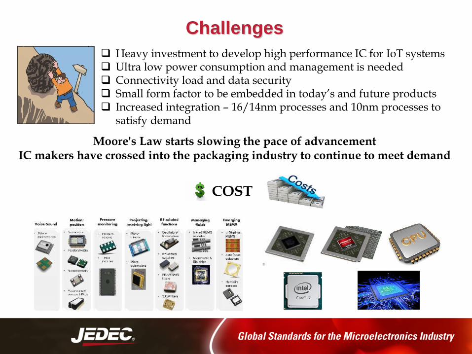
Challenges
Heavy investment to develop high performance IC for IoT systems Ultra low power consumption and management is needed Connectivity load and data security Small form factor to be embedded in today’s and future products Increased integration – 16/14nm processes and 10nm processes to
satisfy demand
COST
Moore's Law starts slowing the pace of advancementIC makers have crossed into the packaging industry to continue to meet demand

Packages Choices
Advanced
packaging
growth
driven by
mobile
products
Wire Bond is Majority
Integrated-circuit packaging has evolved since the 1970s
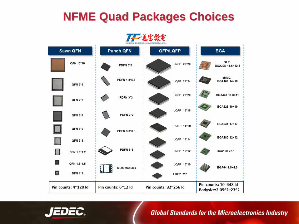
NFME Quad Packages Choices

NFME FC and WLC Packages Choices
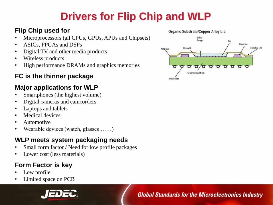
Drivers for Flip Chip and WLP
Flip Chip used for• Microprocessors (all CPUs, GPUs, APUs and Chipsets)
• ASICs, FPGAs and DSPs
• Digital TV and other media products
• Wireless products
• High performance DRAMs and graphics memories
FC is the thinner package
Major applications for WLP• Smartphones (the highest volume)
• Digital cameras and camcorders
• Laptops and tablets
• Medical devices
• Automotive
• Wearable devices (watch, glasses ……)
WLP meets system packaging needs• Small form factor / Need for low profile packages
• Lower cost (less materials)
Form Factor is key• Low profile
• Limited space on PCB

Copper Pillar – Bumping Trends
Demand on 12” Wafers
• Industry is transitioning to Cu Pillar
• Mobile IC makers (Spreadtrum, MTK…) are pioneers to use Cu pillar for mobile
devices
• Intel’s CPUs/GPUs, chipset, FPGAs etc. migrated to use Cu pillar
• Most ASICs and FPGAs migrating to Cu pillar at < 100um pitch

NFME 12” Fully Auto Bumping Line
First Chinese OSAT to provide 12” 28nm Cu pillar full turnkey services

NFME Cu Pillar Process Capability
Dimension Description Current limits
P Bump Pitch ≧ 80um
S Bump Space ≧ 30um
D UBM Diameter ≧ 40um
BHBump Height BH ≦ 70um
Aspect Ratio BH / S ≦ 2
h Solder Cap Height h≦ 70% D
D
P
S
h
BH
LF
Ni
Cu
Ni
LF
Cu
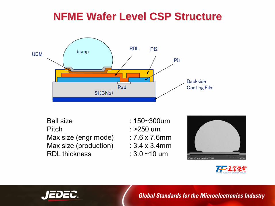
NFME Wafer Level CSP Structure
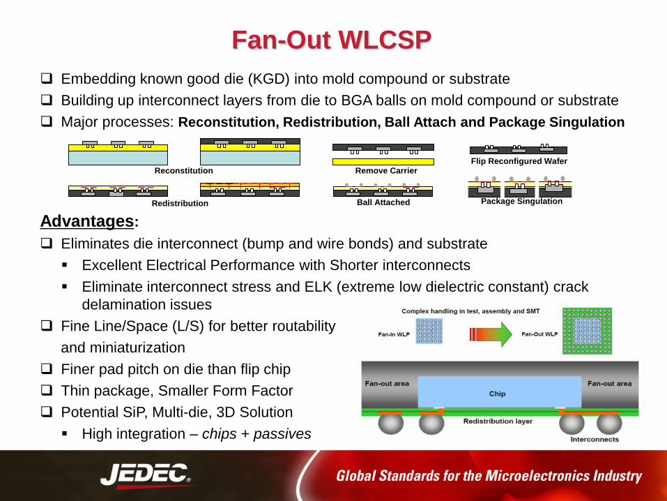
Fan-Out WLCSP
Embedding known good die (KGD) into mold compound or substrate
Building up interconnect layers from die to BGA balls on mold compound or substrate
Major processes: Reconstitution, Redistribution, Ball Attach and Package Singulation
Advantages:
Eliminates die interconnect (bump and wire bonds) and substrate
Excellent Electrical Performance with Shorter interconnects
Eliminate interconnect stress and ELK (extreme low dielectric constant) crack
delamination issues
Fine Line/Space (L/S) for better routability
and miniaturization
Finer pad pitch on die than flip chip
Thin package, Smaller Form Factor
Potential SiP, Multi-die, 3D Solution
High integration – chips + passives
Reconstitution Remove Carrier Flip Reconfigured Wafer
Redistribution Ball Attached Package Singulation

Drivers for Fan-Out WLCSP
Smaller form factor, lower
profile package (less than
0.35mm)
Increased I/O density
Multi-die package/SiP
Excellent electrical and
thermal performance
High reliability is given
Package cost only spent on
Known Good Die
No pad limitation
SiP compatible (2D & 3D)
Advanced WLP will further drive miniaturization of next generation electronic
products
The use of Redistribution Layers (RDL) is an integral part of WLP, in which
processes are being performed at the wafer level instead of the traditional wire
bonding process
Potential for >5.6 billion units shipments in 2020 by TechSearch
Source: Yole
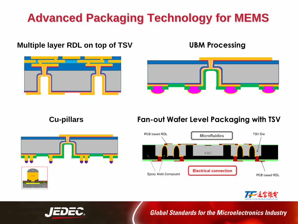
Advanced Packaging Technology for MEMS
Multiple layer RDL on top of TSV UBM Processing
Cu-pillars Fan-out Wafer Level Packaging with TSV
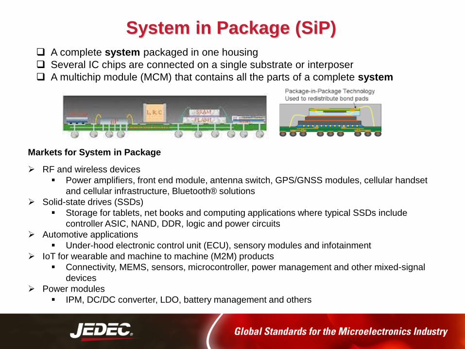
System in Package (SiP)
A complete system packaged in one housing
Several IC chips are connected on a single substrate or interposer
A multichip module (MCM) that contains all the parts of a complete system
Markets for System in Package
RF and wireless devices
Power amplifiers, front end module, antenna switch, GPS/GNSS modules, cellular handset
and cellular infrastructure, Bluetooth® solutions
Solid-state drives (SSDs)
Storage for tablets, net books and computing applications where typical SSDs include
controller ASIC, NAND, DDR, logic and power circuits
Automotive applications
Under-hood electronic control unit (ECU), sensory modules and infotainment
IoT for wearable and machine to machine (M2M) products
Connectivity, MEMS, sensors, microcontroller, power management and other mixed-signal
devices
Power modules
IPM, DC/DC converter, LDO, battery management and others

Power Module Packages Introduction
Intelligent Power Module typically includes 6 IGBTs, 6 Diodes and 3 Driver ICs
1.8mmIC IGBT
DIOD
E 3.1mm
Standard Power Module IGBT Module
Customized DIP modules QFN + MCM = µpower module
Power SiP
Open Tool IPM
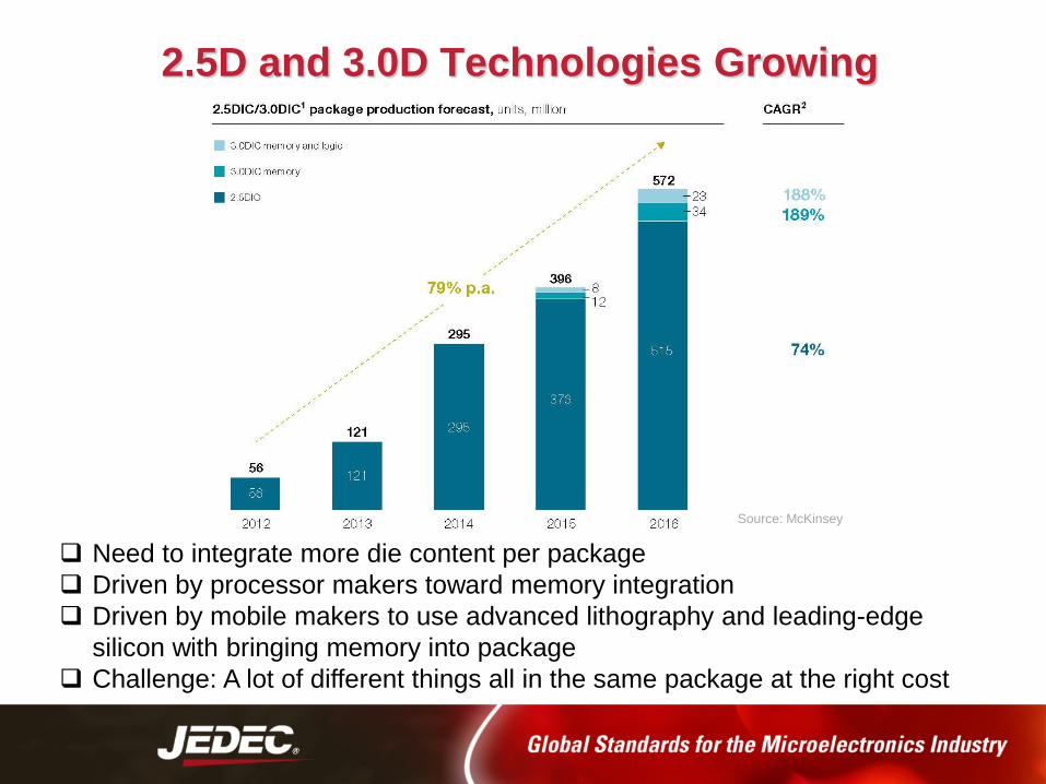
2.5D and 3.0D Technologies Growing
Need to integrate more die content per package
Driven by processor makers toward memory integration
Driven by mobile makers to use advanced lithography and leading-edge
silicon with bringing memory into package
Challenge: A lot of different things all in the same package at the right cost
Source: McKinsey
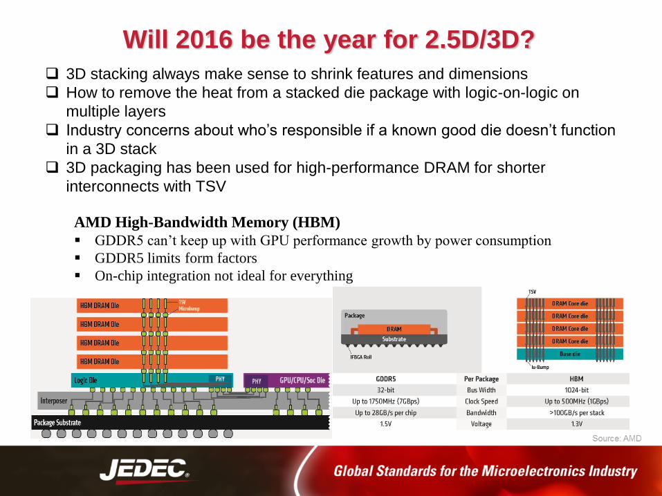
Will 2016 be the year for 2.5D/3D?
AMD High-Bandwidth Memory (HBM)
GDDR5 can’t keep up with GPU performance growth by power consumption
GDDR5 limits form factors
On-chip integration not ideal for everything
3D stacking always make sense to shrink features and dimensions
How to remove the heat from a stacked die package with logic-on-logic on
multiple layers
Industry concerns about who’s responsible if a known good die doesn’t function
in a 3D stack
3D packaging has been used for high-performance DRAM for shorter
interconnects with TSV

Consolidation Impacts on OSAT Business Industry is always developing new and advanced package types – WLP, 2.5D/3D
Advanced packaging requires a significant high investment on R&D and CapEx
OSAT-IDM strategic engagement (JV/M&A) can leverage their advantages to yield
very positive and key inflections points for growth, market share gains
The JV of NFME-AMD creates a strong engineering and operation talents to
develop advanced packages, such as FC-CSP, WLCSP, 2.5D and 3D
NFME will be positioned in a key market segment to drive next generation platforms
crossing several key end markets:- High performance (Server, Graphics, Computing …)
- Mobile (Miniaturization, SiP …)
- IoT (Integrating MCU/Sensors/Memory …)

4,769
3,700
2,6122,520
1,339
730 679 617 606 525 478 456370 360 323 315 276 264 251
0
500
1,000
1,500
2,000
2,500
3,000
3,500
4,000
4,500
5,000
Top
6
NFME-AMD JV – Market Share Expansion

NFME-AMD JV – Package Expansion

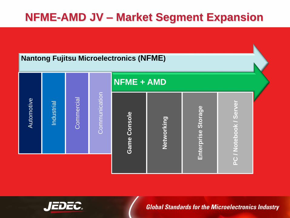
Nantong Fujitsu Microelectronics (NFME)
NFME + AMD
Technology expansion:
• Increase FC I/O up to 3000
• ≥ 14/16nm ELK qualified
• Coreless substrate
• Substrate up to 18 layers
• Increase package size (75mm)
• Increase density, speed & bandwidth
• Adv. SoC hardware development
1st OSAT in China to provide:
- Automotive packaging
- LQFP packaging
- BGA packaging
- MCM packaging
- 28nm Cu Pillar full turnkey
NFME-AMD JV – Technologies Expansion
Nantong Fujitsu Microelectronics (NFME)
NFME + AMD
Au
tom
otive
Ind
ustr
ial
Com
me
rcia
l
Com
mu
nic
atio
n
Gam
e C
on
so
le
Ne
two
rkin
g
En
terp
ris
e S
tora
ge
PC
/ N
ote
bo
ok
/ S
erv
er
NFME-AMD JV – Market Segment Expansion
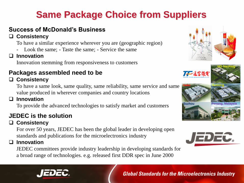
Same Package Choice from Suppliers
Success of McDonald’s Business Consistency
To have a similar experience wherever you are (geographic region)
- Look the same; - Taste the same; - Service the same
Innovation
Innovation stemming from responsiveness to customers
Packages assembled need to be Consistency
To have a same look, same quality, same reliability, same service and same
value produced in wherever companies and country locations
Innovation
To provide the advanced technologies to satisfy market and customers
JEDEC is the solution Consistency
For over 50 years, JEDEC has been the global leader in developing open
standards and publications for the microelectronics industry
Innovation
JEDEC committees provide industry leadership in developing standards for
a broad range of technologies. e.g. released first DDR spec in June 2000
HQ-Nantong
Hefei Nantong
Suzhou Penang, Malaysia

ConclusionsIoT experiencing tremendous growth – Sensing, Processing and Connectivity- Billions of devices in few more years to increase the connectivity
- Many short-range to long-range wireless transmissions to transport IoT data
- The margin of ICs will continually be squeezed for lower cost
- Mobile products require low profile packages: FC-CSP, Fan-in WLP, FO-WLP
Demand for lower cost solutions drives adoption of new package designs- Many different products, many different package types
Moore’s Law slows the pace of advanced silicon technology- Need more packaging, co-package-co-design, closer Silicon to package integration for
electrical, thermal and performance
- Miniaturization drivers Fan-Out WLP, SiP, 2.5D, 3D advanced packages
- 2016 will be the year of 2.5D
Consolidation- Value of OSATs working closely with IDMs who knows the advanced design and systems
- With partner with AMD, NFME can be able to build an ecosystem from supply-chain to
manufacturing to design and produce the advanced future packages
OSATs should produce the packages: same look, same spec, same relibility- Industry 4.0/IoT should be applied by OSATs operations
- OSATs should joint and partner with JEDEC to set up more industry rules
Thank You!