presentation based on transistors
TRANSCRIPT

Presentation Based on Transistor

INTRODUCTION
Transistor is a three terminal electronic device, made up of semiconductor material which generally consist of three parts.
i. Baseii. Emitter iii. Collector
PARTS OF TRANSISTOR
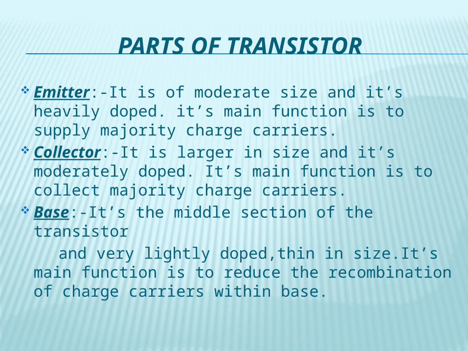
Emitter:-It is of moderate size and it’s heavily doped. it’s main function is to supply majority charge carriers.
Collector:-It is larger in size and it’s moderately doped. It’s main function is to collect majority charge carriers.
Base:-It’s the middle section of the transistor and very lightly doped,thin in size.It’s main
function is to reduce the recombination of charge carriers within base.
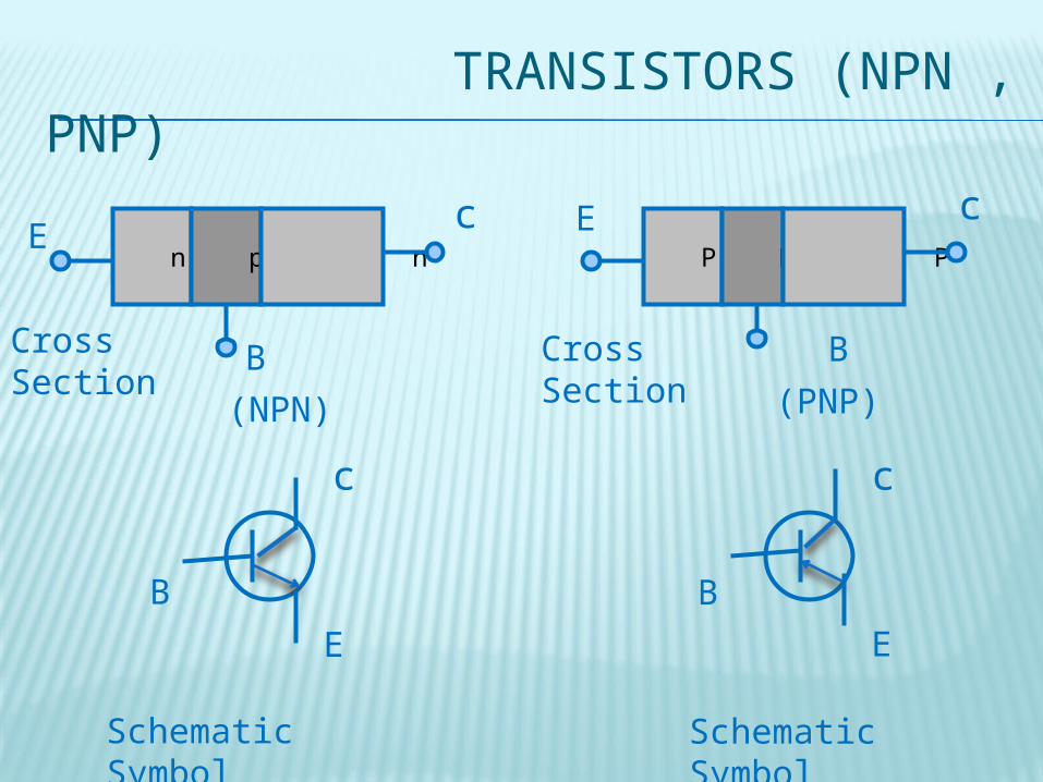
TRANSISTORS (NPN , PNP)
n p nE
B
c
Cross Section
P N P
Cross Section(NPN) (PNP)
E
B
c
Schematic Symbol
Schematic Symbol
EE
BB
cc

TRANSISTOR WORKING PRINCIPLEThe transistor can function as:
An insulator A conductor
The transistor's ability to fluctuate between these two states enables it to switch or amplify.
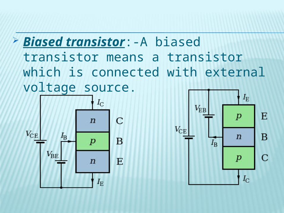
Biased transistor:-A biased transistor means a transistor which is connected with external voltage source.

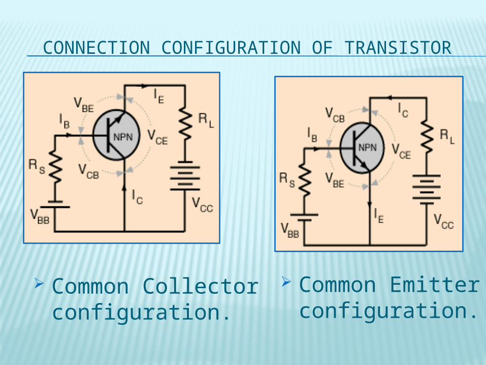
CONNECTION CONFIGURATION OF TRANSISTOR Common base configuration. Common Emitter configuration. Common Collector configuration.
Common base configuration
CONNECTION CONFIGURATION OF TRANSISTOR
Common Emitter configuration.
Common Collector configuration.

WORKING REGION OF TRANSISTOR
Region Emitter Base Junction
Collector Base Junction
Active Forward biased Reverse biased
Cut-off Reverse biased Reverse biased
Saturation Forward biased Forward biased
A biased transistor works in three region:-

OPERATION OF N-P-N TRANSISTOR
Base to Emitter junction is forward
biased by the dc source v . Collector to base junction is reverse
biased by the dc source v . The forward biased EB junction causes
the n type emitter electrons to flow towards base.This constitute emitter current.
Some electrons combine in base region and constitute base current.
Remaining electrons cross base region and move through collector region and it constitute collector current.
BE
CE

OPERATION OF P-N-P TRANSISTOR Base to Emitter junction is forward
biased by the dc source v . Collector to base junction is
reverse biased by the dc source v .
The forward biased EB junction causes the p type emitter hole to flow towards base.This constitute emitter current.
Some hole combine in base region and constitute base current.
Remaining hole cross base region and move through collector region and it constitute collector current.
CE
BE

TRANSISTOR CURRENT
I
II
I I IB
B
E
CC
E
npnIE = IB + IC
pnpIE = IB + IC

TRANSISTOR VOLTAGE
v
vvv v
vCB
BE
CE
CB
BE
CE
npnVCE = -VCB + VBE
pnpVCE = -VCB + VBE

CURRENT GAIN
= Common-emitter current gain
= Common-base current gain
= Common-collector current gain
= IC /I = I /I =I / I
The relationships between the two parameter β + 1 1 -
B B
α = β =
DC and DC α
C E E

TRANSISTOR OPERATION Operation Region Bias Application
CUT OFF REGION IB and Ic are 0 (base-emitter and collector –base junction is reverse biased)
Open Switch (OFF)
SATURATION REGION
Base emitter junction is forward biased; IB flows
Closed Switch (ON)
ACTIVE REGION B-E junction is forward biased but C-B junction is reverse biased;
Amplifier

TRANSISTOR AS A SWITCH

ON MODE

THANK YOU…