probing 5g devices like it’s no big deal · • total handset volume is 1.5b • 10% handsets are...
TRANSCRIPT

Probing 5G DevicesLike It’s No Big Deal
Tim Lesher, Patrick RhodesFormFactor
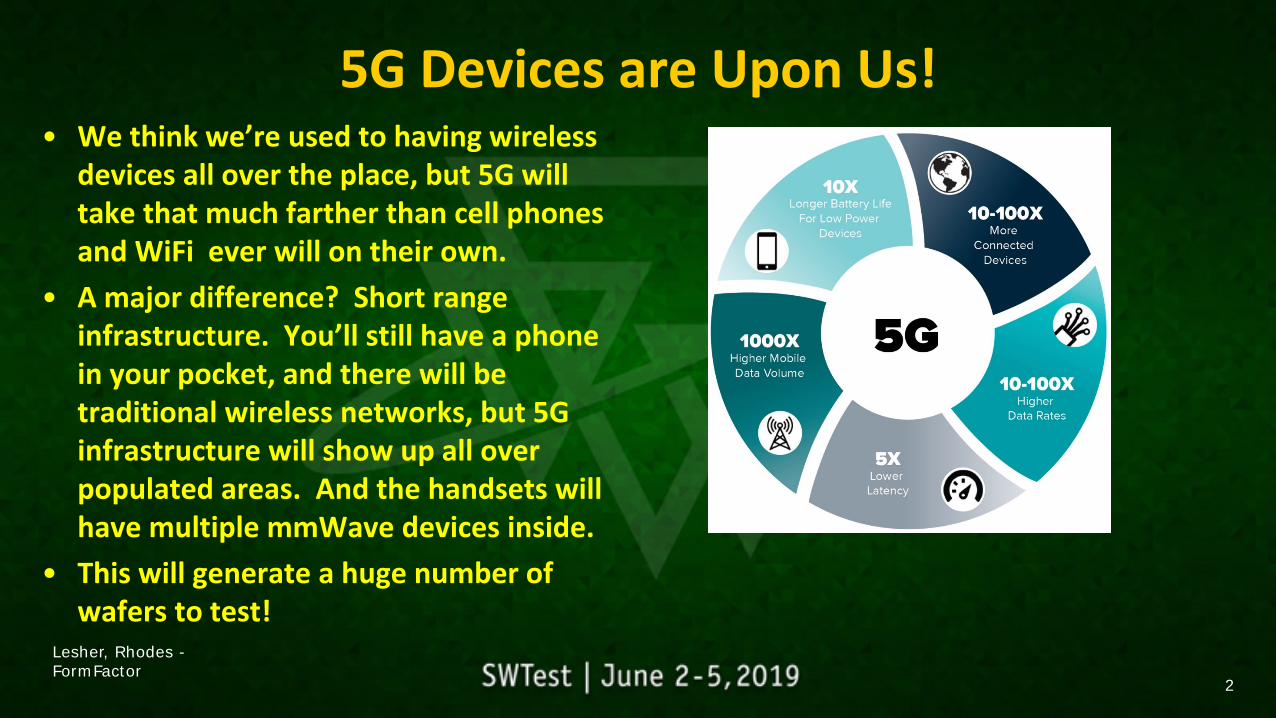
5G Devices are Upon Us!• We think we’re used to having wireless
devices all over the place, but 5G will take that much farther than cell phones and WiFi ever will on their own.
• A major difference? Short range infrastructure. You’ll still have a phone in your pocket, and there will be traditional wireless networks, but 5G infrastructure will show up all over populated areas. And the handsets will have multiple mmWave devices inside.
• This will generate a huge number of wafers to test!
2
Lesher, Rhodes -FormFactor

What Volume Production Means for 5G Test• A long time ago in a galaxy far, far away, people tested DRAM
devices 16 or 32 at a time• DRAM wasn’t found in everything at that time, but now it’s all over
the place• Those people that were testing 16 or 32 devices at a time would be
broke if they did it that way today, but probe technologies advanced to often allow test of a full wafer in one shot
• It won’t scale exactly the same way, but 5G devices may follow a similar path – since they’ll be everywhere, low parallel testing will be an unacceptable bottleneck
– Potential Scenarios:• Total Handset Volume is 1.5B• 10% handsets are 5G FR2• 4 AiP per handset• 600M AiP per year• 90% yield• 5 second test time• 85% test cell OEE for x1, 80% for x8• Probe card lifetime = 1M TDs
– Worldwide Testers: • X1: 125 testers• X8: 16 testers
– Annual Probe heads • Single Site: 667 probe heads• X8 : 89 probe heads
3
DRAM 5G SiP
Lesher, Rhodes - FormFactor
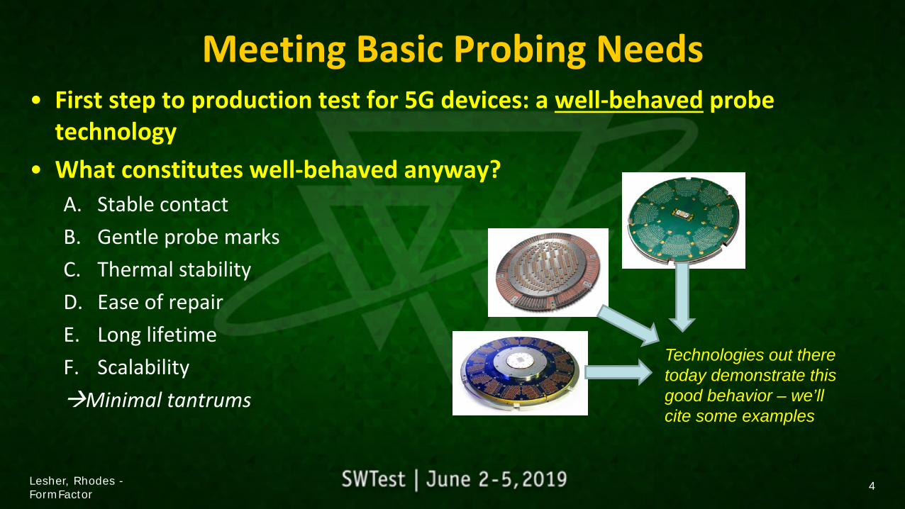
Meeting Basic Probing Needs• First step to production test for 5G devices: a well-behaved probe
technology• What constitutes well-behaved anyway?
A. Stable contactB. Gentle probe marksC. Thermal stabilityD. Ease of repairE. Long lifetimeF. ScalabilityMinimal tantrums
4
Technologies out there today demonstrate this good behavior – we’ll cite some examples
Lesher, Rhodes -FormFactor

Exhibit A – Contact Resistance
– As a function of touchdowns, resistance values are relatively constant without any cleaning over many probing cycles, and can be returned to baseline values with an ordinary cleaning recipe
5
• Any probe technology needs stable contact resistance – for 5G devices or otherwise
• Stability is demonstrated as a function of overtravel and as a function of touchdowns
– As a function of overtravel, resistance values stabilize as soon as the probe reaches its buckling point (2 probes shown reach same stable value)
CRES vs. TDs, Flat Tip on Blank Al Wafer
020000400006000080000
100000120000140000160000180000
0 10 20 30 40 50 60 70 80 90
Resis
tanc
e (m
Ohm
s)
Over Travel(um)
CRES
Pin 8-1 Pin 6-2
Buckling Region
Initial Contact
CRES vs. OT, Flat Tip on Blank Al Wafer
*Absolute resistance values not representative, sub-optimal tip type for flat Al surface
Lesher, Rhodes -FormFactor
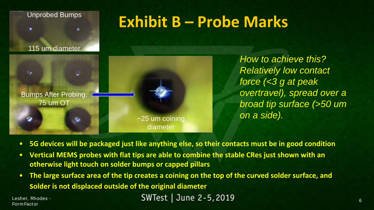
Exhibit B – Probe Marks
• 5G devices will be packaged just like anything else, so their contacts must be in good condition• Vertical MEMS probes with flat tips are able to combine the stable CRes just shown with an
otherwise light touch on solder bumps or capped pillars• The large surface area of the tip creates a coining on the top of the curved solder surface, and
solder is not displaced outside of the original diameter
6
Unprobed Bumps
115 um diameter
Bumps After Probing,75 um OT
~25 um coining diameter
How to achieve this? Relatively low contact force (<3 g at peak overtravel), spread over a broad tip surface (>50 um on a side).
Lesher, Rhodes -FormFactor

Exhibit C – Thermal Stability• There must be an option to test at
extremes of temperature, since 5G devices will be used in environmentally challenging locations– Ex: outside on a pole under bright sunshine
in Phoenix
• Data shown here collected on Uflex + UF3000 test cell for 3-6 GHz RF application
7
• Proximity soak (-200 um) yields 90% of movement within 30 minutes – short time to thermal stability• 9 um maximum movement from 25C start to 125 C finish, on long axis of probe head• Contact soak from t=0 appears allowable due to low magnitude of total movement
– Ready to probe well before 30 minutes – quick setup• Demonstrated capability over 25125C temperature range; higher temperatures remain reasonable
Lesher, Rhodes -FormFactor
Ready, Set, Go!
Time to Thermal Stability (X)
Time, minutes
Posi
tion,
um

Exhibit D – Repairability• Blinding flash of the obvious – bad things sometimes happen
when probing• Vertical MEMS can be quite forgiving of these incidents
– They can withstand an occasional excessive overtravel event and return to original position
– They can be replaced one by one in the event of more serious damage• High current/thermal damage• Breakage for any reason
– They can all be replaced in the event of wearout
8Lesher, Rhodes -FormFactor

Exhibit E – Long Lifetime
• 150 um of wear length with a well-selected material set addresses this
• Wear rates can be fractions of a micron per 1000 cleaning TDs– Data here shows conservative and aggressive recipes – there is room
for optimization for specific applications
9
• Given expected 5G device volumes, quick wear out of probe cards won’t be acceptable
Parameter Z-only 10 um OctagonInterval 10 25 TDsTouches 10 2 Per CycleOT 50 50 umWear rate 0.1 2.4 um/1000 cleaning TDs
150000 31250 Cleaning Cycles1500000 781250 Touchdowns
EOL
Lesher, Rhodes -FormFactor

Exhibit F – ScalabilitySome simple, mathematical-ish relationships:• More contacts, smaller die areafiner pitch• Higher volumeshigher parallelism
10
Vertical MEMS with frequency-capable guide plates can reach down to 106 um grid array pitch. And probe heads are able to support 8+ sites for complex, transceiver-type devices.
Lesher, Rhodes -FormFactor
~4500 probes6 die
High Speed Characteristics
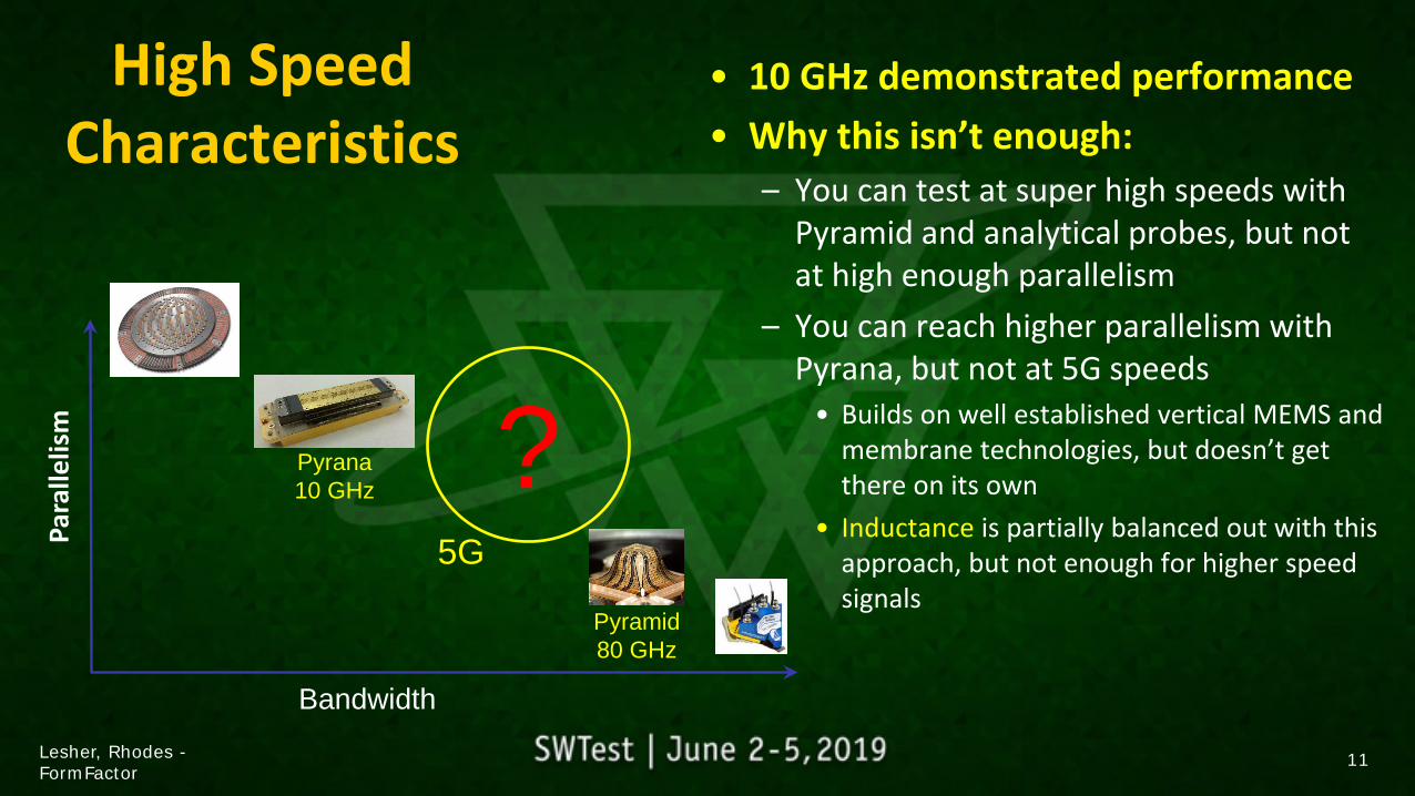
• 10 GHz demonstrated performance• Why this isn’t enough:
– You can test at super high speeds with Pyramid and analytical probes, but not at high enough parallelism
– You can reach higher parallelism with Pyrana, but not at 5G speeds
• Builds on well established vertical MEMS and membrane technologies, but doesn’t get there on its own
• Inductance is partially balanced out with this approach, but not enough for higher speed signals
11
Para
llelis
m
Bandwidth
?5G
Pyrana10 GHz
Pyramid80 GHz
Lesher, Rhodes -FormFactor

Inductance, and How to Stop It• In distributed model of a transmission line, generally R and G
are ignored and Z0=(L/C)^0.5.• With perfect balance for each transition and transmission line,
there is no reflected power and all of the power is transmitted – This never actually happens!
• Vertical probes represent a long path length dominated by high inductance. To compensate:– Shorten the path length– Offset with distributed capacitance– Strategic grounding
12Lesher, Rhodes -FormFactor
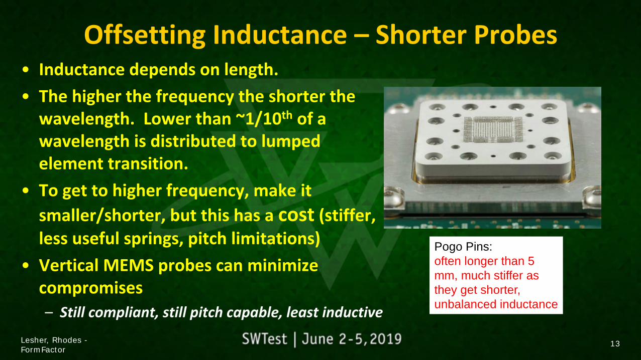
Offsetting Inductance – Shorter Probes• Inductance depends on length.• The higher the frequency the shorter the
wavelength. Lower than ~1/10th of a wavelength is distributed to lumped element transition.
• To get to higher frequency, make it smaller/shorter, but this has a cost (stiffer, less useful springs, pitch limitations)
• Vertical MEMS probes can minimize compromises– Still compliant, still pitch capable, least inductive
13
Pogo Pins: often longer than 5 mm, much stiffer as they get shorter, unbalanced inductance
Lesher, Rhodes -FormFactor

Offsetting Inductance – Parasitic Capacitance• The length of residual inductance is what really matters.• The inductance of a coax cable center conductor is not relevant
because the capacitance to the shield compensates.
14Lesher, Rhodes -FormFactor

Offsetting Inductance• Bringing ground close to the probe tip along with parasitic capacitance to
ground dramatically reduces residual inductance– The physical length and mechanical attributes of the MEMS probes are decoupled
from their electrical length and attributes, by an order of magnitude
15Lesher, Rhodes -FormFactor

Results
16
• Together, this is where it takes us:– 75 mm length array – >250 RF paths up to 45GHz– >4500 contacts– Still on good behavior as a probe technology!
Lesher, Rhodes -FormFactor

S-Parameters – Probe Head and Start of PCB
17
Probe head – PCB interface Tier 1 Probe head – PCB interface Tier 2
Lesher, Rhodes -FormFactor

One Additional Item• With inductance often comes mutual inductance which can
degrade isolation dramatically.• Measured Isolation is better than 30dB for typical device layouts
to 40GHz.• For special cases, isolation can be increased even further
18Lesher, Rhodes -FormFactor
Wrap Up• The advances to higher frequencies are now applicable IN
CONJUNCTION with well-behaved probe technology– Solid mechanical foundation– Electrically resilient– And now supports 5G signals up to 45 GHz
19Lesher, Rhodes -FormFactor
Thank You!• Contacts:
– Tim Lesher, RF Design Engineer – [email protected]– Patrick Rhodes, Product Engineer – [email protected]
20Lesher, Rhodes -FormFactor