product specification - electrodragon · product specification this product specification contains...
TRANSCRIPT
All rights reserved.Reproduction in whole or in part is prohibited without the prior written permission of the copyright holder.
April 2008
Product Specification
Key Features
• True single chip GFSK transceiver in a small 32 pin package (32L QFN 5x5mm)
• ShockBurst™ mode for low power operation• Power supply range 1.9 to 3.6 V• Multi channel operation – ETSI/FCC Compatible • Channel switching time <650µs• Extremely low cost Bill of Material (BOM) • No external SAW filter• Adjustable output power up to 10dBm• Carrier detect for "listen before transmit" protocols• Data Ready signal when a valid data packet is
received or transmitted• Address Match for detection of incoming packet• Automatic retransmission of data packet• Automatic CRC and preamble generation• Low supply current (TX), typical 9mA @ -10dBm out-
put power• Low supply current (RX), typical 12.5mA
Applications
• Wireless data communication• Alarm and security system• Home automation• Remote control• Surveillance• Automotive• Telemetry• Keyless entry• Toys
nRF905
Single chip 433/868/915MHz Transceiver
nRF905 Product Specification
Liability disclaimer
Nordic Semiconductor ASA reserves the right to make changes without further notice to the product to improve reliability, function or design. Nordic Semiconductor ASA does not assume any liability arising out of the application or use of any product or circuits described herein.
All application information is advisory and does not form part of the specification.
Limiting values
Stress above one or more of the limiting values may cause permanent damage to the device. These are stress ratings only and operation of the device at these or at any other conditions above those given in the specifications are not implied. Exposure to limiting values for extended periods may affect device reliability.
Life support applications
These products are not designed for use in life support appliances, devices, or systems where malfunction of these products can reasonably be expected to result in personal injury. Nordic Semiconductor ASA cus-tomers using or selling these products for use in such applications do so at their own risk and agree to fully indemnify Nordic Semiconductor ASA for any damages resulting from such improper use or sale.
Contact details
Visit www.nordicsemi.no for Nordic Semiconductor sales offices and distributors worldwide
Main office:
Otto Nielsens vei 127004 Trondheim
Phone: +47 72 89 89 00 Fax: +47 72 89 89 89www.nordicsemi.no
Data sheet statusObjective product specification This product specification contains target specifications for product
development.Preliminary product specification This product specification contains preliminary data; supplementary
data may be published from Nordic Semiconductor ASA later.Product specification This product specification contains final product specifications. Nordic
Semiconductor ASA reserves the right to make changes at any time without notice in order to improve design and supply the best possible product.
Revision 1.5 Page 2 of 41
nRF905 Product Specification
Writing conventions
This product specification follows a set of typographic rules that makes the document consistent and easy to read. The following writing conventions are used:
• Commands, bit state conditions, and register names are written in Courier.
• Pin names and pin signal conditions are written in Courier bold.
• Cross references are underlined and highlighted in blue.
Revision history
Attention!
Datasheet order code: 051005nRF905
Date Version DescriptionJune 2006 1.4April 2008 1.5 • Restructured layout in the new template
• Updated package information• Added moisture sensitivity level to the absolute maximum ratings
Observe precaution for handling Electrostatic Sensitive Device.
Revision 1.5 Page 3 of 41
nRF905 Product Specification
Contents1 Introduction ............................................................................................... 62 Quick reference data................................................................................. 73 Block Diagram ........................................................................................... 84 Absolute maximum ratings ...................................................................... 95 Electrical Specifications........................................................................... 106 Current Consumption ............................................................................... 137 Pin information.......................................................................................... 147.1 Pin Assignment ................................................................................... 147.2 Pin Functions ....................................................................................... 158 Modes of Operation ................................................................................. 168.1 Active Modes ....................................................................................... 168.2 Power Saving Modes .......................................................................... 168.3 nRF ShockBurst™ Mode ..................................................................... 168.4 Typical ShockBurst™ TX .................................................................... 168.5 Typical ShockBurst™ RX..................................................................... 188.6 Power Down Mode............................................................................... 198.7 Standby Mode ...................................................................................... 199 Device Configuration ............................................................................... 209.1 SPI Register Configuration................................................................... 209.2 SPI Instruction Set .............................................................................. 219.3 SPI Timing............................................................................................ 219.4 RF – Configuration Register Description.............................................. 239.5 Register Contents ................................................................................ 2410 Important Timing Data .............................................................................. 2610.1 Device Switching Times ....................................................................... 2610.2 ShockBurst™ TX timing ....................................................................... 2610.3 ShockBurst™ RX timing....................................................................... 2710.4 Preamble.............................................................................................. 2710.5 Time On Air .......................................................................................... 2711 Peripheral RF Information ........................................................................ 2811.1 Crystal Specification............................................................................. 2811.2 External Clock Reference ................................................................... 2811.3 Microprocessor Output Clock............................................................... 2811.4 Antenna Output .................................................................................... 2911.5 Output Power Adjustment .................................................................... 2911.6 Modulation ........................................................................................ 2911.7 Output Frequency ................................................................................ 2911.8 PCB Layout and Decoupling Guidelines .............................................. 3012 nRF905 features ....................................................................................... 3112.1 Carrier Detect ....................................................................................... 3112.2 Address Match ..................................................................................... 3112.3 Data Ready .......................................................................................... 3112.4 Auto Retransmit ................................................................................... 3112.5 RX Reduced Power Mode.................................................................... 3213 Mechanical specifications........................................................................ 33
Revision 1.5 Page 4 of 41
nRF905 Product Specification
14 Ordering information................................................................................. 3414.1 Package marking.................................................................................. 3414.1.1 Abbreviations ................................................................................... 3414.2 Product options..................................................................................... 3414.2.1 RF silicon ......................................................................................... 3414.2.2 Development tools ........................................................................... 3415 Application Examples ............................................................................... 3515.1 Differential Connection to a Loop Antenna........................................... 3515.2 PCB Layout Example; Differential Connection to a Loop Antenna....... 3615.3 Single ended connection to 50W antenna............................................ 3715.4 PCB Layout Example; Single Ended Connection to 50W Antenna ...... 4016 Glossary of terms ..................................................................................... 41
Revision 1.5 Page 5 of 41
nRF905 Product Specification
1 Introduction
nRF905 is a single chip radio transceiver for the 433/868/915MHz ISM band. The transceiver consists of a fully integrated frequency synthesizer, receiver chain with demodulator, a power amplifier, a crystal oscilla-tor and, a modulator. The ShockBurst™ feature automatically handles preamble and CRC. You can easily configure the nRF905 through the SPI. Current consumption is very low, in transmit only 9mA at an output power of -10dBm, and in receive mode 12.5mA. Built-in power down modes makes power saving easily realizable.
Revision 1.5 Page 6 of 41
nRF905 Product Specification
2 Quick reference data
Table 1. nRF905 quick reference data.
Parameter Value UnitMinimum supply voltage 1.9 VMaximum transmit output power 10 dBmData rate 50 kbpsSupply current in transmit @ -10dBm output power 9 mASupply current in receive mode 12.5 mATemperature range -40 to +85 °CTypical sensitivity -100 dBmSupply current in power down mode 2.5 µA
Revision 1.5 Page 7 of 41
nRF905 Product Specification
3 Block Diagram
Figure 1. nRF905 with external components.
SPIinterface
ShockBurst
Demod
Dataslicer
Addressdecode
CRC code/decode
GFSKfilter
RX - reg.Config-reg.
TX - reg.TX - addr.
PA
LNAIF
BB
F
FrequencySynthesiser
Voltageregulators
Crystaloscillator
MOSI (11)
MISO (10)
SCK (12)
CSN (13)
TRX_CE (1)
PWR_UP (2)
TX_EN (32)
CD (6)
AM (7)
DR (8)
uPCLK (3)
XC1 (14)
XC2 (15)
ANT1 (20)
ANT2 (21)
VDD_PA (19)
VS
S (5)
VS
S (16)
VS
S (18)
VS
S (22)
VS
S (24)
VS
S (27)
VS
S (28)
VS
S (29)
VS
S (30)
VD
D (4)
VD
D (17)
VD
D (25)
DV
DD
_1V2 (31)
IREF (23)
Manchesterencoder/decoder
VS
S (26)
VS
S (9)
Revision 1.5 Page 8 of 41
nRF905 Product Specification
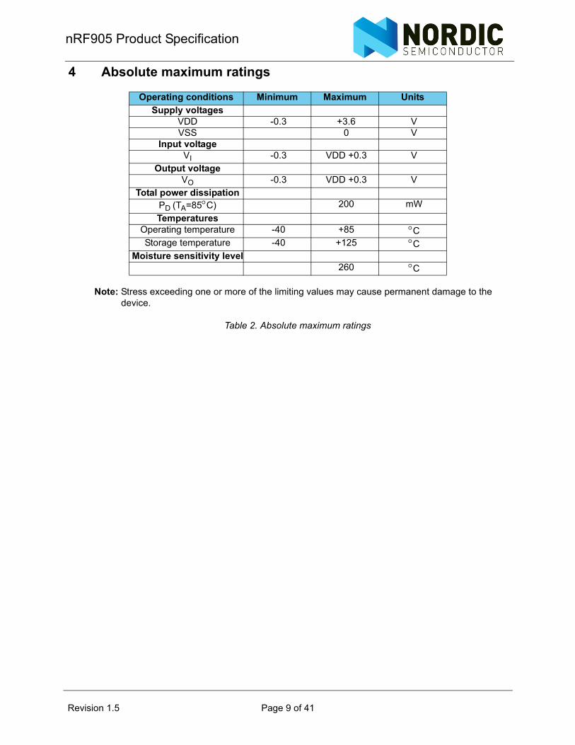
4 Absolute maximum ratings
Note: Stress exceeding one or more of the limiting values may cause permanent damage to the device.
Table 2. Absolute maximum ratings
Operating conditions Minimum Maximum UnitsSupply voltages
VDD -0.3 +3.6 VVSS 0 V
Input voltageVI -0.3 VDD +0.3 V
Output voltageVO -0.3 VDD +0.3 V
Total power dissipationPD (TA=85°C) 200 mWTemperatures
Operating temperature -40 +85 °CStorage temperature -40 +125 °C
Moisture sensitivity level260 °C
Revision 1.5 Page 9 of 41
nRF905 Product Specification
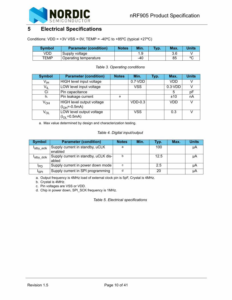
5 Electrical Specifications
Conditions: VDD = +3V VSS = 0V, TEMP = -40ºC to +85ºC (typical +27ºC)
Table 3. Operating conditions
Table 4. Digital input/output
Table 5. Electrical specifications
Symbol Parameter (condition) Notes Min. Typ. Max. UnitsVDD Supply voltage 1.9 3.6 V
TEMP Operating temperature -40 85 ºC
Symbol Parameter (condition) Notes Min. Typ. Max. UnitsVIH HIGH level input voltage 0.7·VDD VDD VVIL LOW level input voltage VSS 0.3·VDD VCi Pin capacitance 5 pFIiL Pin leakage current a
a. Max value determined by design and characterization testing.
±10 nAVOH HIGH level output voltage
(IOH=-0.5mA)VDD-0.3 VDD V
VOL LOW level output voltage (IOL=0.5mA)
VSS 0.3 V
Symbol Parameter (condition) Notes Min. Typ. Max. UnitsIstby_eclk Supply current in standby, uCLK
enabled a
a. Output frequency is 4MHz load of external clock pin is 5pF, Crystal is 4MHz.
100 µA
Istby_dclk Supply current in standby, uCLK dis-abled
b
b. Crystal is 4MHz.
12.5 µA
IPD Supply current in power down mode c
c. Pin voltages are VSS or VDD.
2.5 µAISPI Supply current in SPI programming d
d. Chip in power down, SPI_SCK frequency is 1MHz.
20 µA
Revision 1.5 Page 10 of 41
nRF905 Product Specification
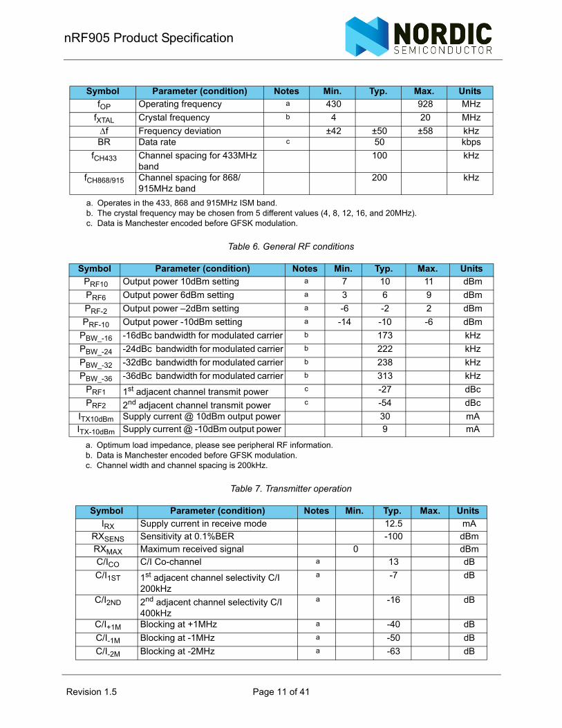
Table 6. General RF conditions
Table 7. Transmitter operation
Symbol Parameter (condition) Notes Min. Typ. Max. UnitsfOP Operating frequency a
a. Operates in the 433, 868 and 915MHz ISM band.
430 928 MHzfXTAL Crystal frequency b
b. The crystal frequency may be chosen from 5 different values (4, 8, 12, 16, and 20MHz).
4 20 MHzΔf Frequency deviation ±42 ±50 ±58 kHzBR Data rate c
c. Data is Manchester encoded before GFSK modulation.
50 kbpsfCH433 Channel spacing for 433MHz
band100 kHz
fCH868/915 Channel spacing for 868/915MHz band
200 kHz
Symbol Parameter (condition) Notes Min. Typ. Max. UnitsPRF10 Output power 10dBm setting a
a. Optimum load impedance, please see peripheral RF information.
7 10 11 dBmPRF6 Output power 6dBm setting a 3 6 9 dBmPRF-2 Output power –2dBm setting a -6 -2 2 dBmPRF-10 Output power -10dBm setting a -14 -10 -6 dBm
PBW_-16 -16dBc bandwidth for modulated carrier b
b. Data is Manchester encoded before GFSK modulation.
173 kHzPBW_-24 -24dBc bandwidth for modulated carrier b 222 kHzPBW_-32 -32dBc bandwidth for modulated carrier b 238 kHzPBW_-36 -36dBc bandwidth for modulated carrier b 313 kHz
PRF1 1st adjacent channel transmit power c
c. Channel width and channel spacing is 200kHz.
-27 dBcPRF2 2nd adjacent channel transmit power c -54 dBc
ITX10dBm Supply current @ 10dBm output power 30 mAITX-10dBm Supply current @ -10dBm output power 9 mA
Symbol Parameter (condition) Notes Min. Typ. Max. UnitsIRX Supply current in receive mode 12.5 mA
RXSENS Sensitivity at 0.1%BER -100 dBmRXMAX Maximum received signal 0 dBmC/ICO C/I Co-channel a 13 dBC/I1ST 1st adjacent channel selectivity C/I
200kHza -7 dB
C/I2ND 2nd adjacent channel selectivity C/I 400kHz
a -16 dB
C/I+1M Blocking at +1MHz a -40 dBC/I-1M Blocking at -1MHz a -50 dBC/I-2M Blocking at -2MHz a -63 dB
Revision 1.5 Page 11 of 41
nRF905 Product Specification
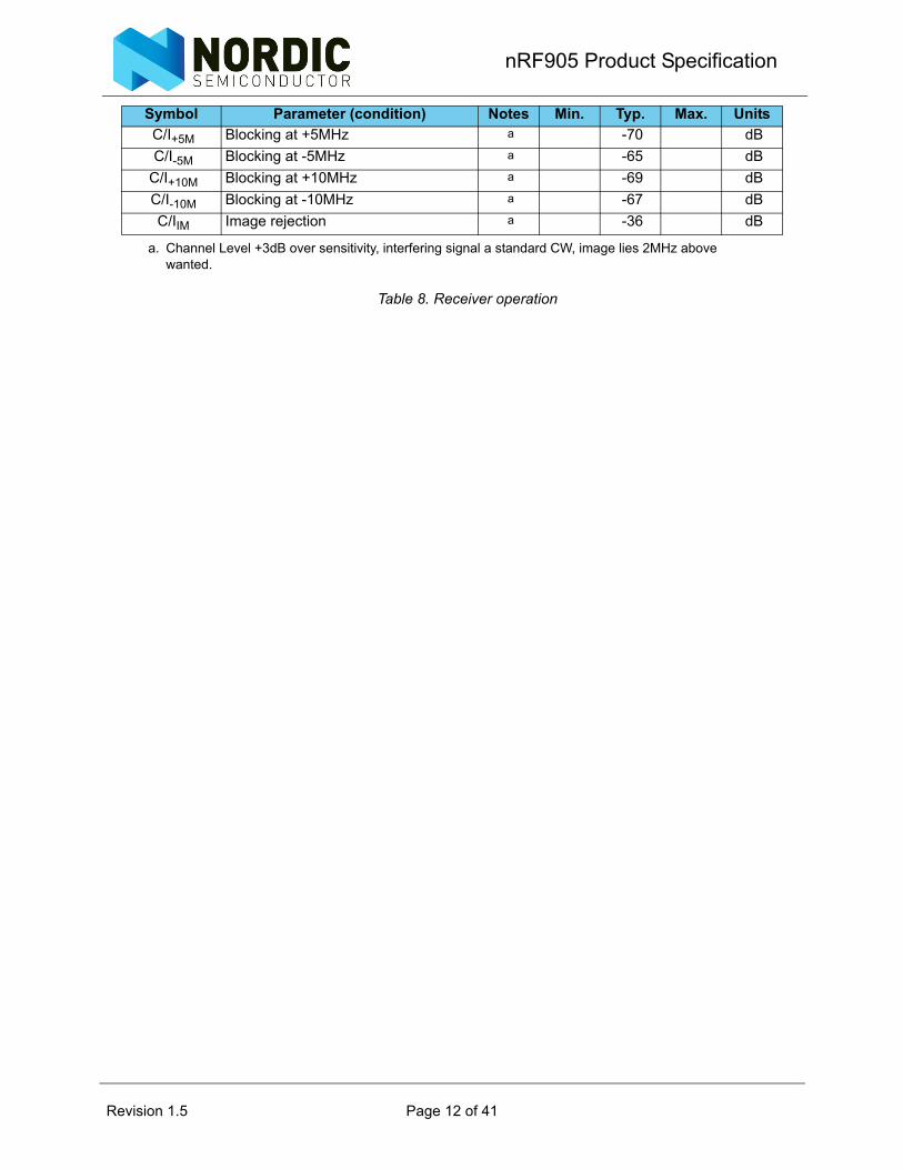
Table 8. Receiver operation
C/I+5M Blocking at +5MHz a -70 dBC/I-5M Blocking at -5MHz a -65 dB
C/I+10M Blocking at +10MHz a -69 dBC/I-10M Blocking at -10MHz a -67 dBC/IIM Image rejection a -36 dB
a. Channel Level +3dB over sensitivity, interfering signal a standard CW, image lies 2MHz above wanted.
Symbol Parameter (condition) Notes Min. Typ. Max. Units
Revision 1.5 Page 12 of 41
nRF905 Product Specification
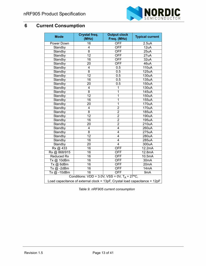
6 Current Consumption
Table 9. nRF905 current consumption
Mode Crystal freq. (MHz)
Output clock Freq. (MHz) Typical current
Power Down 16 OFF 2.5uAStandby 4 OFF 12uAStandby 8 OFF 25uAStandby 12 OFF 27uAStandby 16 OFF 32uAStandby 20 OFF 46uAStandby 4 0.5 110uAStandby 8 0.5 125uAStandby 12 0.5 130uAStandby 16 0.5 135uAStandby 20 0.5 150uAStandby 4 1 130uAStandby 8 1 145uAStandby 12 1 150uAStandby 16 1 155uAStandby 20 1 170uAStandby 4 2 170uAStandby 8 2 185uAStandby 12 2 190uAStandby 16 2 195uAStandby 20 2 210uAStandby 4 4 260uAStandby 8 4 275uAStandby 12 4 280uAStandby 16 4 285uAStandby 20 4 300uA
Rx @ 433 16 OFF 12.2mARx @ 868/915 16 OFF 12.8mAReduced Rx 16 OFF 10.5mATx @ 10dBm 16 OFF 30mATx @ 6dBm 16 OFF 20mATx @ -2dBm 16 OFF 14mATx @ -10dBm 16 OFF 9mA
Conditions: VDD = 3.0V, VSS = 0V, TA = 27ºC, Load capacitance of external clock = 13pF, Crystal load capacitance = 12pF
Revision 1.5 Page 13 of 41
nRF905 Product Specification
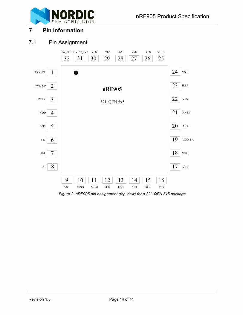
7 Pin information
7.1 Pin Assignment
Figure 2. nRF905 pin assignment (top view) for a 32L QFN 5x5 package
nRF905
32L QFN 5x5
MOSI
VSS
CD
DVDD_1V2
AM
XC2 VSS
DR
VSS
ANT2
VDD_PA
VSS
ANT1
VSS
VSS VDD
VSS
TRX_CE
XC1
4
3
2
1
6
5
7
8
9 13 1412 1510 11 16
24
23
22
20
19
21
18
17
29 28 2730 26 253132
VDD
VSSTX_EN
IREF
VSS VSS VSS
MISO
PWR_UP
uPCLK
VDD
CSNSCK
Revision 1.5 Page 14 of 41
nRF905 Product Specification
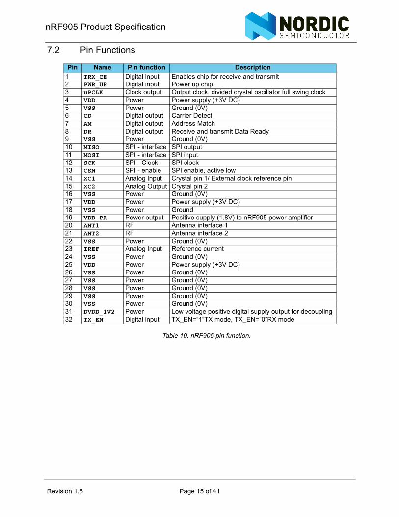
7.2 Pin Functions
Table 10. nRF905 pin function.
Pin Name Pin function Description1 TRX_CE Digital input Enables chip for receive and transmit 2 PWR_UP Digital input Power up chip3 uPCLK Clock output Output clock, divided crystal oscillator full swing clock 4 VDD Power Power supply (+3V DC) 5 VSS Power Ground (0V)6 CD Digital output Carrier Detect7 AM Digital output Address Match8 DR Digital output Receive and transmit Data Ready 9 VSS Power Ground (0V)10 MISO SPI - interface SPI output11 MOSI SPI - interface SPI input12 SCK SPI - Clock SPI clock13 CSN SPI - enable SPI enable, active low14 XC1 Analog Input Crystal pin 1/ External clock reference pin15 XC2 Analog Output Crystal pin 216 VSS Power Ground (0V)17 VDD Power Power supply (+3V DC) 18 VSS Power Ground19 VDD_PA Power output Positive supply (1.8V) to nRF905 power amplifier20 ANT1 RF Antenna interface 121 ANT2 RF Antenna interface 222 VSS Power Ground (0V)23 IREF Analog Input Reference current24 VSS Power Ground (0V)25 VDD Power Power supply (+3V DC)26 VSS Power Ground (0V)27 VSS Power Ground (0V)28 VSS Power Ground (0V)29 VSS Power Ground (0V)30 VSS Power Ground (0V)31 DVDD_1V2 Power Low voltage positive digital supply output for decoupling32 TX_EN Digital input TX_EN=”1”TX mode, TX_EN=”0”RX mode
Revision 1.5 Page 15 of 41
nRF905 Product Specification
8 Modes of Operation
The nRF905 has two active (RX/TX) modes and two power saving modes:
8.1 Active Modes
• ShockBurst™ RX• ShockBurst™ TX
8.2 Power Saving Modes
• Power down and SPI programming• Standby and SPI programming
The nRF905 mode is decided by the settings of TRX_CE, TX_EN and PWR_UP.
Table 11. nRF905 operational modes.
8.3 nRF ShockBurst™ Mode
The nRF905 uses the ShockBurst™ feature. ShockBurst™ makes it possible to use the high data rate offered by the nRF905 without the need of a costly, high-speed microcontroller (MCU) for data processing/clock recovery. By placing all high speed signal processing related to RF protocol on-chip, the nRF905 offers the application microcontroller a simple SPI, the data rate is decided by the interface speed the microcontroller sets up. By allowing the digital part of the application to run at low speed, while maximizing the data rate on the RF link, the nRF905 ShockBurst™ mode reduces the average current consumption in applications. In ShockBurst™ RX, Address Match (AM) and Data Ready (DR) notifies the MCU when a valid address and payload is received respectively. In ShockBurst™ TX, the nRF905 automatically gener-ates preamble and CRC. Data Ready (DR) notifies the MCU that the transmission is completed. This means reduced memory demand in the MCU resulting in a low cost MCU, as well as reduced software development time.
8.4 Typical ShockBurst™ TX
1. When the application MCU has data for a remote node, the address of the receiving node (TX-address) and payload data (TX-payload) are clocked into nRF905 through the SPI. The applica-tion protocol or MCU sets the speed of the interface.
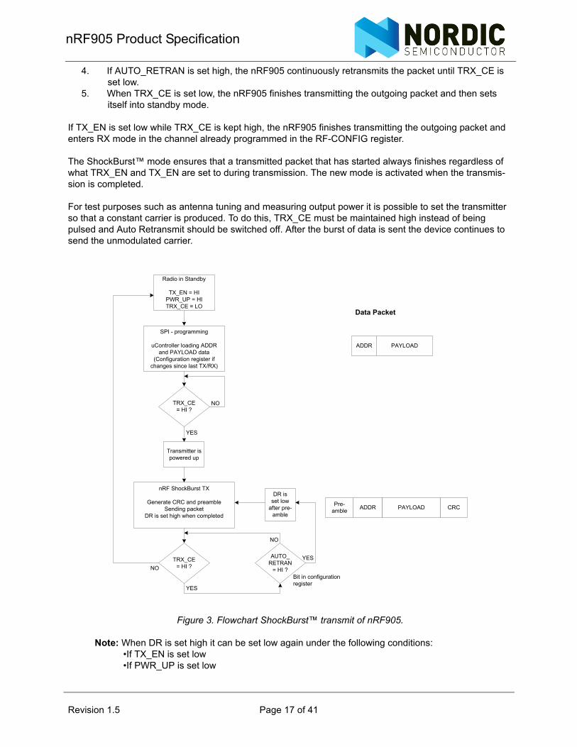
2. MCU sets TRX_CE and TX_EN high, this activates a nRF905 ShockBurst™ transmission.3. nRF905 ShockBurst™ does the following:
Radio is automatically powered up.Data packet is completed (preamble added, CRC calculated).Data packet is transmitted (50kbps).Data Ready is set high when transmission is completed.
PWR_UP TRX_CE TX_EN Operating Mode0 X X Power down and SPI programming1 0 X Standby and SPI programming1 X 0 Read data from RX register1 1 0 Radio Enabled - ShockBurst™ RX1 1 1 Radio Enabled - ShockBurst™ TX
Revision 1.5 Page 16 of 41
nRF905 Product Specification
4. If AUTO_RETRAN is set high, the nRF905 continuously retransmits the packet until TRX_CE is set low.
5. When TRX_CE is set low, the nRF905 finishes transmitting the outgoing packet and then sets itself into standby mode.
If TX_EN is set low while TRX_CE is kept high, the nRF905 finishes transmitting the outgoing packet and enters RX mode in the channel already programmed in the RF-CONFIG register.
The ShockBurst™ mode ensures that a transmitted packet that has started always finishes regardless of what TRX_EN and TX_EN are set to during transmission. The new mode is activated when the transmis-sion is completed.
For test purposes such as antenna tuning and measuring output power it is possible to set the transmitter so that a constant carrier is produced. To do this, TRX_CE must be maintained high instead of being pulsed and Auto Retransmit should be switched off. After the burst of data is sent the device continues to send the unmodulated carrier.
Figure 3. Flowchart ShockBurst™ transmit of nRF905.
Note: When DR is set high it can be set low again under the following conditions:•If TX_EN is set low•If PWR_UP is set low
SPI - programming
uController loading ADDRand PAYLOAD data
(Configuration register if changes since last TX/RX)
NO
YES
nRF ShockBurst TX
Generate CRC and preambleSending packet
DR is set high when completed
Transmitter is powered up
TRX_CE= HI ?
AUTO_RETRAN
= HI ?
YES
NO
YES
NO
ADDR PAYLOAD
Data Packet
Bit in configuration register
TRX_CE= HI ?
Radio in Standby
TX_EN = HIPWR_UP = HITRX_CE = LO
ADDR PAYLOAD CRCPre-amble
DR is set low
after pre-amble
Revision 1.5 Page 17 of 41

nRF905 Product Specification
8.5 Typical ShockBurst™ RX
1. ShockBurst™ RX is selected by setting TRX_CE high and TX_EN low.2. After 650µs nRF905 is monitoring the air for incoming communication.3. When the nRF905 senses a carrier at the receiving frequency, Carrier Detect (CD) pin is set high.4. When a valid address is received, Address Match (AM) pin is set high.5. When a valid packet has been received (correct CRC found), nRF905 removes the preamble,
address and CRC bits, and the Data Ready (DR) pin is set high. 6. MCU sets the TRX_CE low to enter standby mode (low current mode).7. MCU can clock out the payload data at a suitable rate through the SPI. 8. When all payload data is retrieved, nRF905 sets Data Ready (DR) and Address Match (AM) low
again. 9. The chip is now ready for entering ShockBurst™ RX, ShockBurst™ TX or, power down mode.
If TX_EN is set high while TRX_CE is kept high, the nRF905 would enter ShockBurst™ TX and start a transmission according to the present contents in the SPI registers.
If TRX_CE or TX_EN is changed during an incoming packet, the nRF905 changes mode immediately and the packet is lost. However, if the MCU is sensing the Address Match (AM) pin, it knows when the chip is receiving an incoming packet and can therefore decide whether to wait for the Data Ready (DR) signal or enter a different mode.
To avoid spurious address matches it is recommended that the address length be 24 bits or higher in length. Small addresses such as 8 or 16 bits can often lead to statistical failures due to the address being repeated as part of the data packet. This can be avoided by using a longer address.
Each byte within the address should be unique. Repeating bytes within the address reduces the effective-ness of the address and increases its susceptibility to noise which increases the packet error rate. The address should also have several level shifts (that is, 10101100) reducing the statistical effect of noise and the packet error rate.
Revision 1.5 Page 18 of 41

nRF905 Product Specification
Figure 4. Flowchart ShockBurst™ receive of nRF905.
8.6 Power Down Mode
In power down the nRF905 is disabled with minimal current consumption, typically less than 2.5µA. When the device enters this mode it is not active which minimizes average current consumption and maximizes battery lifetime. The configuration word content is maintained during power down.
8.7 Standby Mode
Standby mode is used to minimize average current consumption while maintaining short start up times to ShockBurst™ RX and ShockBurst™ TX. In this mode part of the crystal oscillator is active. Current con-sumption is dependent on crystal frequency, Ex: IDD= 12µA @4MHz and IDD =46µA @20MHz. If the uP-clock (pin 3) of nRF905 is enabled, current consumption increases and is dependent on the load capaci-tance and frequency. The configuration word content is maintained during standby.
NO
YES
Receiver is powered up
NO
YES
Receiving data
ReceiverSensing for incomming data
CD is set high if carrier
AM is set high
NO
DR high is set high
Radio enters STBY
MCU clocks out payload via the SPI interface
DR and AM are set lowYES
YES
NOAM is set low
Radio in StandbyTX_EN = LO
PWR_UP = HI
TRX_CE= HI ?
CorrectADDR?
CorrectCRC?
TRX_CE = HI ?
PAYLOAD
Data Packet
ADDR PAYLOAD CRCPre-amble
RX Remains On
MCU clocks out payload via the SPI interface
DR and AM are set low
Revision 1.5 Page 19 of 41

nRF905 Product Specification
9 Device Configuration
All configuration of the nRF905 is through the SPI. The interface consists of five registers. A SPI instruction set is used to decide which operation shall be performed. The SPI can be activated in any mode however, we recommend that the chip is in standby or power down mode.
9.1 SPI Register Configuration
The SPI consists of five internal registers. A register readback mode is implemented to allow verification of the register contents.
Figure 5. SPI – interface and the five internal registers.
Table 12. Internal registers description
Internal registers DescriptionStatus – Register Register contains status of Data Ready (DR), Address Match (AM).
RF – Configuration Register Register contains transceiver setup information such as frequency and output power ext.
TX – Address Register contains address of target device. How many bytes used is set in the configuration register.
TX – Payload Register containing the payload information to be sent in a Shock-Burst™ packet. How many bytes used is set in the configuration regis-ter.
RX – Payload Register containing the payload information derived from a received valid ShockBurst ™ packet. How many bytes used is set in the configu-ration register. Valid data in the RX-Payload register is indicated with a high Date Ready (DR) signal.
TX-PAYLOADENDTACLK
I/O-regCSN
MOSI
MISO
SCK
RF - CONFIGURATIONREGISTER
ENDTACLK
TX-ADDRESSENDTACLK
RX-PAYLOADENDTACLK
STATUS-REGISTERENDTACLK
Revision 1.5 Page 20 of 41
nRF905 Product Specification
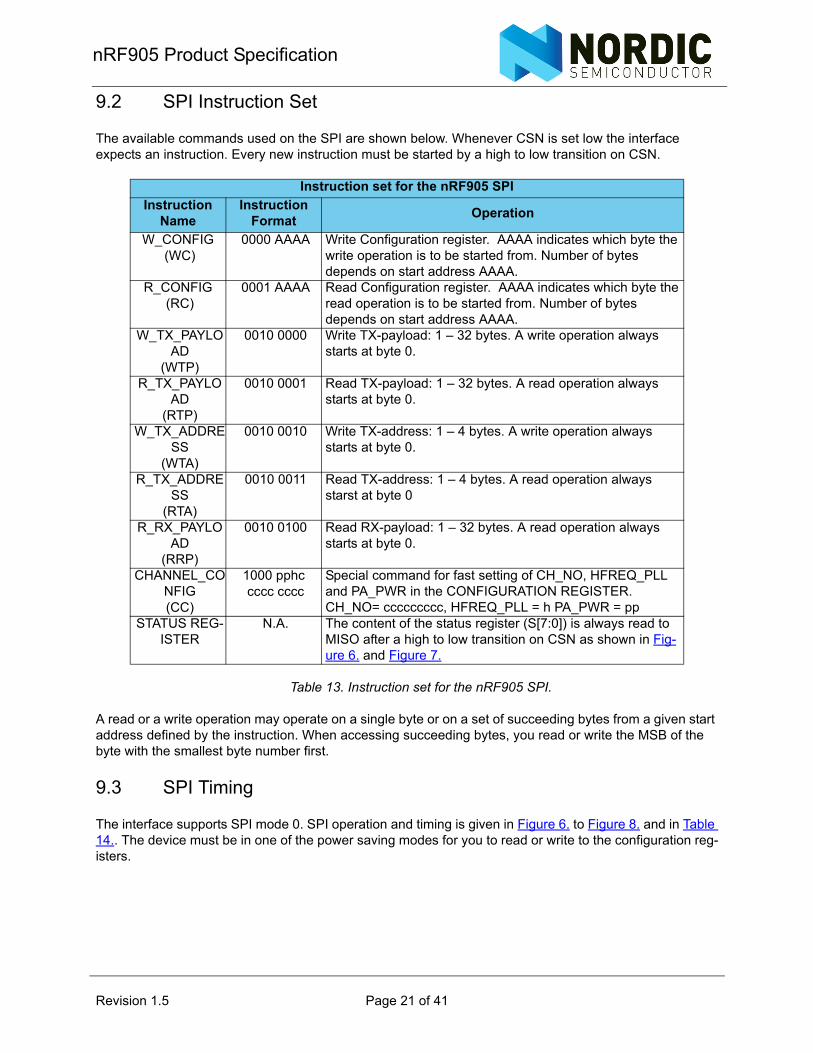
9.2 SPI Instruction Set
The available commands used on the SPI are shown below. Whenever CSN is set low the interface expects an instruction. Every new instruction must be started by a high to low transition on CSN.
Table 13. Instruction set for the nRF905 SPI.
A read or a write operation may operate on a single byte or on a set of succeeding bytes from a given start address defined by the instruction. When accessing succeeding bytes, you read or write the MSB of the byte with the smallest byte number first.
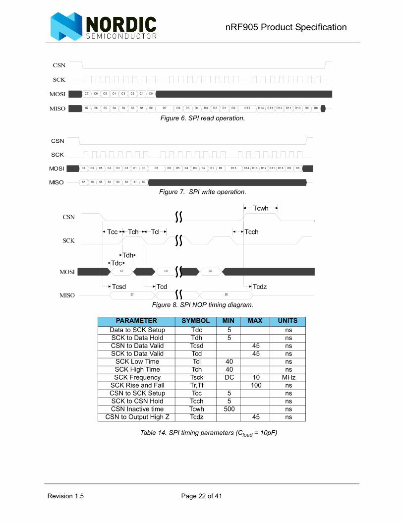
9.3 SPI Timing
The interface supports SPI mode 0. SPI operation and timing is given in Figure 6. to Figure 8. and in Table 14.. The device must be in one of the power saving modes for you to read or write to the configuration reg-isters.
Instruction set for the nRF905 SPIInstruction
NameInstruction
Format Operation
W_CONFIG (WC)
0000 AAAA Write Configuration register. AAAA indicates which byte the write operation is to be started from. Number of bytes depends on start address AAAA.
R_CONFIG (RC)
0001 AAAA Read Configuration register. AAAA indicates which byte the read operation is to be started from. Number of bytes depends on start address AAAA.
W_TX_PAYLOAD
(WTP)
0010 0000 Write TX-payload: 1 – 32 bytes. A write operation always starts at byte 0.
R_TX_PAYLOAD
(RTP)
0010 0001 Read TX-payload: 1 – 32 bytes. A read operation always starts at byte 0.
W_TX_ADDRESS
(WTA)
0010 0010 Write TX-address: 1 – 4 bytes. A write operation always starts at byte 0.
R_TX_ADDRESS
(RTA)
0010 0011 Read TX-address: 1 – 4 bytes. A read operation always starst at byte 0
R_RX_PAYLOAD
(RRP)
0010 0100 Read RX-payload: 1 – 32 bytes. A read operation always starts at byte 0.
CHANNEL_CONFIG(CC)
1000 pphc cccc cccc
Special command for fast setting of CH_NO, HFREQ_PLL and PA_PWR in the CONFIGURATION REGISTER. CH_NO= ccccccccc, HFREQ_PLL = h PA_PWR = pp
STATUS REG-ISTER
N.A. The content of the status register (S[7:0]) is always read to MISO after a high to low transition on CSN as shown in Fig-ure 6. and Figure 7.
Revision 1.5 Page 21 of 41
nRF905 Product Specification
Figure 6. SPI read operation.
Figure 7. SPI write operation.
Figure 8. SPI NOP timing diagram.
Table 14. SPI timing parameters (Cload = 10pF)
PARAMETER SYMBOL MIN MAX UNITSData to SCK Setup Tdc 5 nsSCK to Data Hold Tdh 5 nsCSN to Data Valid Tcsd 45 nsSCK to Data Valid Tcd 45 ns
SCK Low Time Tcl 40 nsSCK High Time Tch 40 nsSCK Frequency Tsck DC 10 MHz
SCK Rise and Fall Tr,Tf 100 nsCSN to SCK Setup Tcc 5 nsSCK to CSN Hold Tcch 5 nsCSN Inactive time Tcwh 500 ns
CSN to Output High Z Tcdz 45 ns
C7 C6 C5 C4 C3 C2 C1 C0
S7 S6 S5 S4 S3 S2 S1 S0 D7 D6 D5 D4 D3 D2 D1 D0 D15 D14 D13 D12 D1 1 D10 D9 D8
CSN
SCK
MOSI
MISO
C7 C6 C5 C4 C3 C2 C1 C0 D7 D6 D5 D4 D3 D2 D1 D0 D15 D14 D13 D12 D11 D1 0 D9 D8
S7 S6 S5 S4 S3 S2 S1 S0
CSN
SCK
MOSI
MISO
C7 C6 C0
S7 S0
TcdzTcdTcsd
TdhTdc
TcchTclTclTchTcc Tch
TcwhTcwhCSN
SCK
MOSI
MISO
Revision 1.5 Page 22 of 41
nRF905 Product Specification
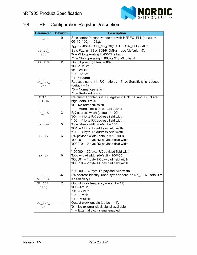
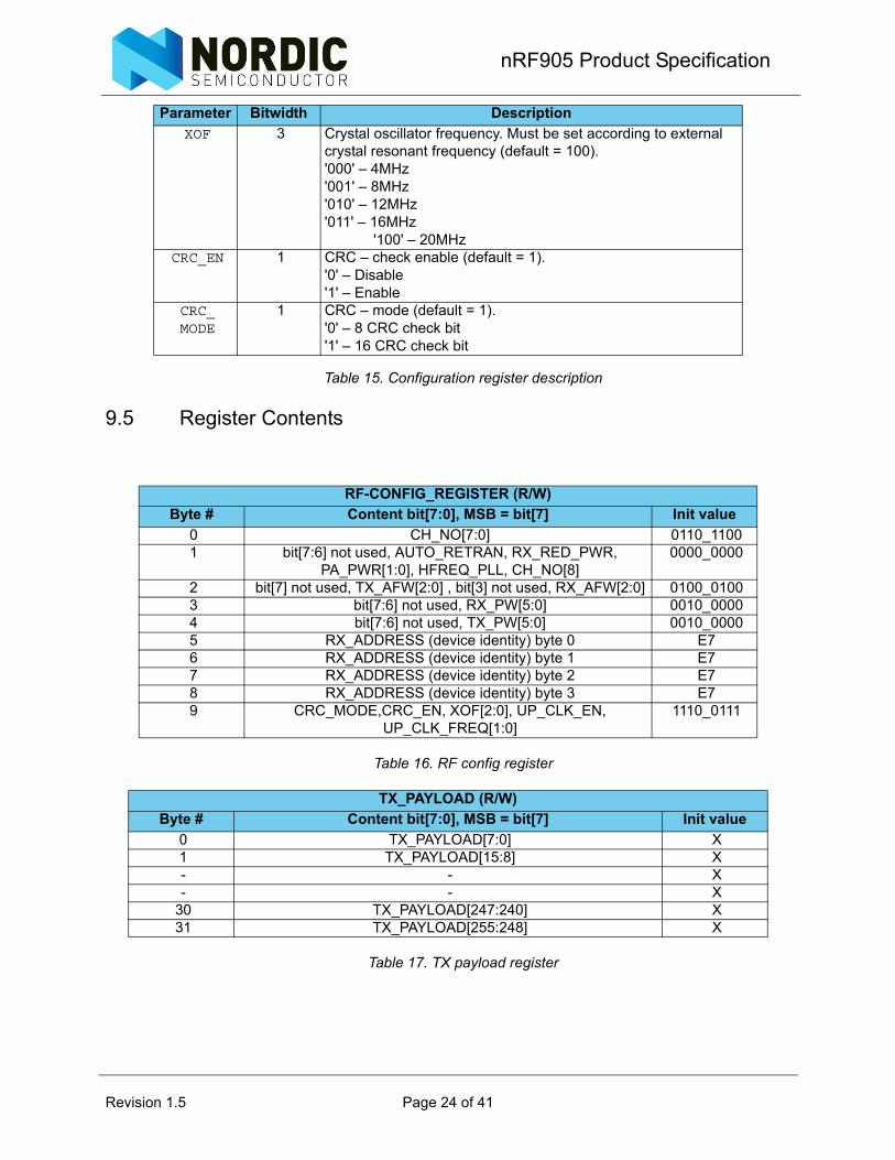
9.4 RF – Configuration Register Description
Parameter Bitwidth DescriptionCH_NO 9 Sets center frequency together with HFREQ_PLL (default =
001101100b = 108d). fRF = ( 422.4 + CH_NOd /10)*(1+HFREQ_PLLd) MHz
HFREQ_PLL
1 Sets PLL in 433 or 868/915MHz mode (default = 0).'0' – Chip operating in 433MHz band '1' – Chip operating in 868 or 915 MHz band
PA_PWR 2 Output power (default = 00).'00' -10dBm'01' -2dBm'10' +6dBm'11' +10dBm
RX_RED_PWR
1 Reduces current in RX mode by 1.6mA. Sensitivity is reduced (default = 0). '0' – Normal operation '1' – Reduced power
AUTO_RETRAN
1 Retransmit contents in TX register if TRX_CE and TXEN are high (default = 0). '0' – No retransmission '1' – Retransmission of data packet
RX_AFW 3 RX-address width (default = 100). '001' – 1 byte RX address field width'100' – 4 byte RX address field width
TX_AFW 3 TX-address width (default = 100). '001' – 1 byte TX address field width'100' – 4 byte TX address field width
RX_PW 6 RX-payload width (default = 100000).'000001' – 1 byte RX payload field width'000010' – 2 byte RX payload field width .'100000' – 32 byte RX payload field width
TX_PW 6 TX-payload width (default = 100000).'000001' – 1 byte TX payload field width'000010' – 2 byte TX payload field width .'100000' – 32 byte TX payload field width
RX_ADDRESS
32 RX address identity. Used bytes depend on RX_AFW (default = E7E7E7E7h).
UP_CLK_FREQ
2 Output clock frequency (default = 11).'00' – 4MHz '01' – 2MHz'10' – 1MHz'11' – 500kHz
UP_CLK_EN
1 Output clock enable (default = 1).'0' – No external clock signal available'1' – External clock signal enabled
Revision 1.5 Page 23 of 41
nRF905 Product Specification
Table 15. Configuration register description
9.5 Register Contents
Table 16. RF config register
Table 17. TX payload register
XOF 3 Crystal oscillator frequency. Must be set according to external crystal resonant frequency (default = 100).'000' – 4MHz'001' – 8MHz'010' – 12MHz'011' – 16MHz '100' – 20MHz
CRC_EN 1 CRC – check enable (default = 1).'0' – Disable'1' – Enable
CRC_MODE
1 CRC – mode (default = 1).'0' – 8 CRC check bit'1' – 16 CRC check bit
RF-CONFIG_REGISTER (R/W)Byte # Content bit[7:0], MSB = bit[7] Init value
0 CH_NO[7:0] 0110_11001 bit[7:6] not used, AUTO_RETRAN, RX_RED_PWR,
PA_PWR[1:0], HFREQ_PLL, CH_NO[8]0000_0000
2 bit[7] not used, TX_AFW[2:0] , bit[3] not used, RX_AFW[2:0] 0100_01003 bit[7:6] not used, RX_PW[5:0] 0010_00004 bit[7:6] not used, TX_PW[5:0] 0010_00005 RX_ADDRESS (device identity) byte 0 E76 RX_ADDRESS (device identity) byte 1 E77 RX_ADDRESS (device identity) byte 2 E78 RX_ADDRESS (device identity) byte 3 E79 CRC_MODE,CRC_EN, XOF[2:0], UP_CLK_EN,
UP_CLK_FREQ[1:0]1110_0111
TX_PAYLOAD (R/W)Byte # Content bit[7:0], MSB = bit[7] Init value
0 TX_PAYLOAD[7:0] X1 TX_PAYLOAD[15:8] X- - X- - X
30 TX_PAYLOAD[247:240] X31 TX_PAYLOAD[255:248] X
Parameter Bitwidth Description
Revision 1.5 Page 24 of 41
nRF905 Product Specification
Table 18.TX address register
Table 19. RX payload register
Table 20. Status register
The length of all registers is fixed. However, the bytes in TX_PAYLOAD, RX_PAYLOAD, TX_ADDRESS and RX_ADDRESS used in ShockBurst™ RX/TX are set in the configuration register. Register content is not lost when the device enters one of the power saving modes.
TX_ADDRESS (R/W)Byte # Content bit[7:0], MSB = bit[7] Init value
0 TX_ADDRESS[7:0] E71 TX_ADDRESS[15:8] E72 TX_ADDRESS[23:16] E73 TX_ADDRESS[31:24] E7
RX_PAYLOAD (R)Byte # Content bit[7:0], MSB = bit[7] Init value
0 RX_PAYLOAD[7:0] X1 RX_PAYLOAD[15:8] X
- X- X
30 RX_PAYLOAD[247:240] X31 RX_PAYLOAD[255:248] X
STATUS_REGISTER (R)Byte # Content bit[7:0], MSB = bit[7] Init value
0 AM, bit [6] not used, DR, bit [0:4] not used X
Revision 1.5 Page 25 of 41
nRF905 Product Specification
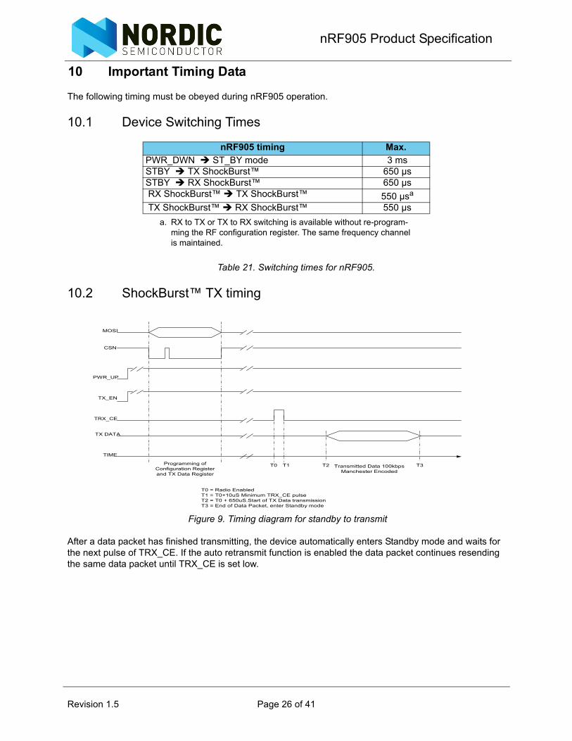
10 Important Timing Data
The following timing must be obeyed during nRF905 operation.
10.1 Device Switching Times
Table 21. Switching times for nRF905.
10.2 ShockBurst™ TX timing
Figure 9. Timing diagram for standby to transmit
After a data packet has finished transmitting, the device automatically enters Standby mode and waits for the next pulse of TRX_CE. If the auto retransmit function is enabled the data packet continues resending the same data packet until TRX_CE is set low.
nRF905 timing Max.PWR_DWN ST_BY mode 3 ms STBY TX ShockBurst™ 650 µsSTBY RX ShockBurst™ 650 µs RX ShockBurst™ TX ShockBurst™ 550 µsa
a. RX to TX or TX to RX switching is available without re-program-ming the RF configuration register. The same frequency channel is maintained.
TX ShockBurst™ RX ShockBurst™ 550 µs
MOSI
CSN
PWR_UP
TX_EN
TRX_CE
TX DATA
TIME
T0 = Radio EnabledT1 = T0+10uS Minimum TRX_CE pulseT2 = T0 + 650uS.Start of TX Data transmissionT3 = End of Data Packet, enter Standby mode
Programming ofConfiguration Registerand TX Data Register
T0 T1 T2 T3Transmitted Data 100kbpsManchester Encoded
Revision 1.5 Page 26 of 41

nRF905 Product Specification
10.3 ShockBurst™ RX timing
Figure 10. Timing diagram for standby to receiving
After the Data Ready (DR) has been set high a valid data packet is available in the RX data register. This may be clocked out in RX mode or standby mode. After the data has been clocked out through the SPI the Data Ready (DR) and Address Match (AM) pins are reset to low.
The RX register is reset if the PWR_UP pin is taken low or if the device is switched into TX mode, that is, TXEN is taken high. This also results in the Data Ready (DR) and Address Match (AM) pins being reset to low.
10.4 Preamble
In each data packet transmitted by the nRF905 a preamble is added automatically. The preamble is a pre-defined bit sequence used to adjust the receiver for optimal performance. A ten bit sequence is used as preamble in nRF905. The length of the preamble, tpreamble, is then 200µs.
10.5 Time On Air
The time on air is the sum of the radio start up time and the data packet length. The length of the preamble, address field, payload and CRC checksum give the data packet length while the radio start up time is given in Table 11. While preamble length and start up time are fixed the user sets the other parameters in the RF configuration register. The below equation shows how to calculate TOA:
tstartup and tpreamble are RF start up time and preamble time respectively. Naddress, Npayload and NCRC are numbers of bits in the address, payload and CRC checksum while BR is the bitrate, which is equal to 50kbps.
PWR_UP
TX_EN
TRX_CE
RX DATA
TIME
AM
DR
CD
T0 = Receiver Enabled -Listening for DataT1 = Carrier Detect finds a carrierT2 = AM - Correct Address FoundT3 = DR - Data packet with correct Address/CRC
650uS to enter RXmode fromTRX_CE being sethigh.
T0 T1 T2 T3
650uS
BRNNN
ttTOA CRCpayloadaddresspreamblestartup
++++=
Revision 1.5 Page 27 of 41
nRF905 Product Specification
11 Peripheral RF Information
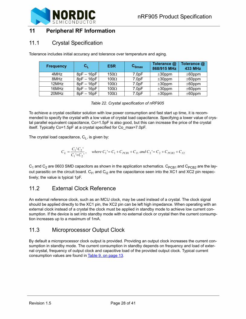
11.1 Crystal Specification
Tolerance includes initial accuracy and tolerance over temperature and aging.
Table 22. Crystal specification of nRF905
To achieve a crystal oscillator solution with low power consumption and fast start up time, it is recom-mended to specify the crystal with a low value of crystal load capacitance. Specifying a lower value of crys-tal parallel equivalent capacitance, Co=1.5pF is also good, but this can increase the price of the crystal itself. Typically Co=1.5pF at a crystal specified for Co_max=7.0pF.
The crystal load capacitance, CL, is given by:
C1 and C2 are 0603 SMD capacitors as shown in the application schematics. CPCB1 and CPCB2 are the lay-out parasitic on the circuit board. CI1 and CI2 are the capacitance seen into the XC1 and XC2 pin respec-tively; the value is typical 1pF.
11.2 External Clock Reference
An external reference clock, such as an MCU clock, may be used instead of a crystal. The clock signal should be applied directly to the XC1 pin, the XC2 pin can be left high impedance. When operating with an external clock instead of a crystal the clock must be applied in standby mode to achieve low current con-sumption. If the device is set into standby mode with no external clock or crystal then the current consump-tion increases up to a maximum of 1mA.
11.3 Microprocessor Output Clock
By default a microprocessor clock output is provided. Providing an output clock increases the current con-sumption in standby mode. The current consumption in standby depends on frequency and load of exter-nal crystal, frequency of output clock and capacitive load of the provided output clock. Typical current consumption values are found in Table 9. on page 13.
Frequency CL ESR C0maxTolerance @ 868/915 MHz
Tolerance @ 433 MHz
4MHz 8pF – 16pF 150Ω 7.0pF ±30ppm ±60ppm8MHz 8pF – 16pF 100Ω 7.0pF ±30ppm ±60ppm12MHz 8pF – 16pF 100Ω 7.0pF ±30ppm ±60ppm16MHz 8pF – 16pF 100Ω 7.0pF ±30ppm ±60ppm20MHz 8pF – 16pF 100Ω 7.0pF ±30ppm ±60ppm
2222111121
21 '',''''
IPCBIPCBL CCCCandCCCCwhereCCCC
C ++=++=+⋅
=
Revision 1.5 Page 28 of 41
nRF905 Product Specification
11.4 Antenna Output
The ANT1 and ANT2 output pins provide a balanced RF output to the antenna. The pins must have a DC path to VDD_PA, either through a RF choke or through the center point in a dipole antenna. The load impedance seen between the ANT1/ANT2 outputs should be in the range 200-700W. The optimum differ-ential load impedance at the antenna ports is given as:
900MHz225Ω+j210
430MHz300Ω+j100
A low load impedance (for instance 50Ω) can be obtained by fitting a simple matching network or a RF transformer (balun). Further information regarding balun structures and matching networks may be found in chapter 15 on page 35.
11.5 Output Power Adjustment
The power amplifier in nRF905 can be programmed to four different output power settings by the configu-ration register. By reducing output power, the total TX current is reduced.
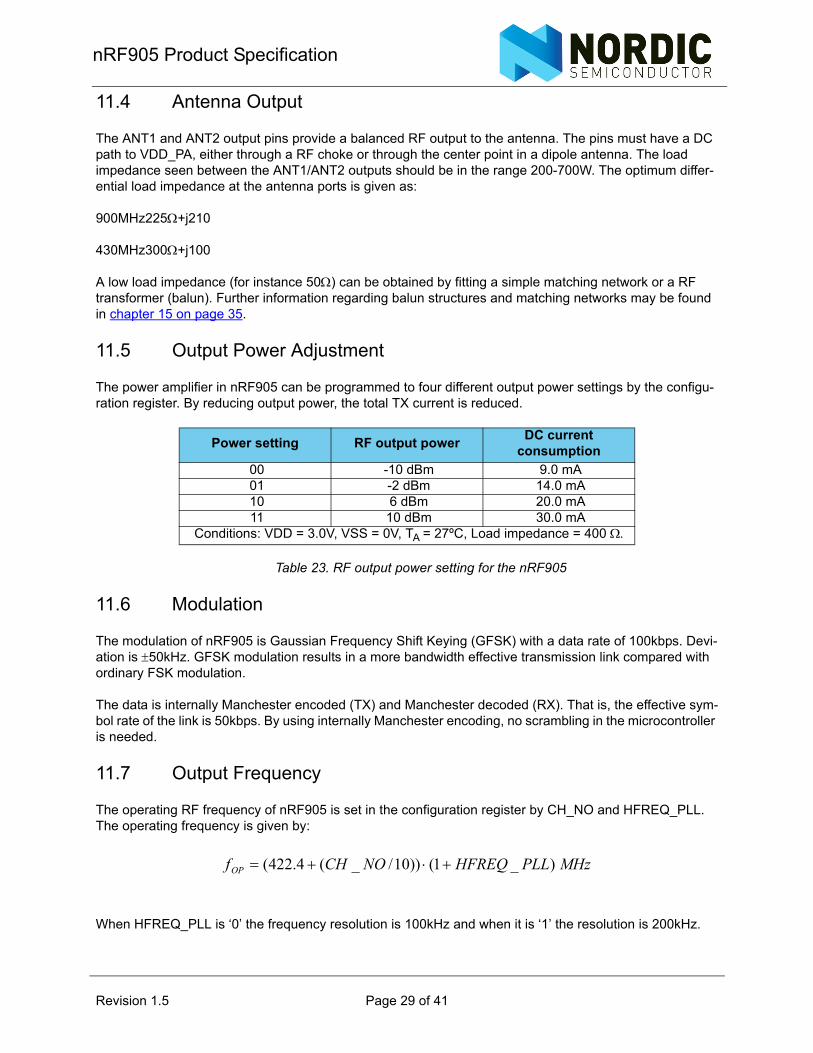
Table 23. RF output power setting for the nRF905
11.6 Modulation
The modulation of nRF905 is Gaussian Frequency Shift Keying (GFSK) with a data rate of 100kbps. Devi-ation is ±50kHz. GFSK modulation results in a more bandwidth effective transmission link compared with ordinary FSK modulation.
The data is internally Manchester encoded (TX) and Manchester decoded (RX). That is, the effective sym-bol rate of the link is 50kbps. By using internally Manchester encoding, no scrambling in the microcontroller is needed.
11.7 Output Frequency
The operating RF frequency of nRF905 is set in the configuration register by CH_NO and HFREQ_PLL. The operating frequency is given by:
When HFREQ_PLL is ‘0’ the frequency resolution is 100kHz and when it is ‘1’ the resolution is 200kHz.
Power setting RF output power DC current consumption
00 -10 dBm 9.0 mA01 -2 dBm 14.0 mA10 6 dBm 20.0 mA11 10 dBm 30.0 mA
Conditions: VDD = 3.0V, VSS = 0V, TA = 27ºC, Load impedance = 400 Ω.
MHzPLLHFREQNOCHfOP )_1())10/_(4.422( +⋅+=
Revision 1.5 Page 29 of 41
nRF905 Product Specification
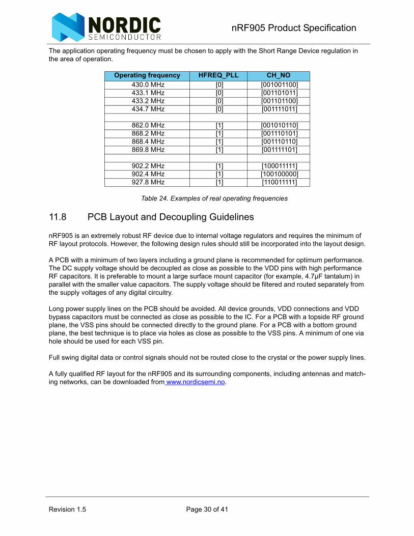
The application operating frequency must be chosen to apply with the Short Range Device regulation in the area of operation.
Table 24. Examples of real operating frequencies
11.8 PCB Layout and Decoupling Guidelines
nRF905 is an extremely robust RF device due to internal voltage regulators and requires the minimum of RF layout protocols. However, the following design rules should still be incorporated into the layout design.
A PCB with a minimum of two layers including a ground plane is recommended for optimum performance. The DC supply voltage should be decoupled as close as possible to the VDD pins with high performance RF capacitors. It is preferable to mount a large surface mount capacitor (for example, 4.7µF tantalum) in parallel with the smaller value capacitors. The supply voltage should be filtered and routed separately from the supply voltages of any digital circuitry.
Long power supply lines on the PCB should be avoided. All device grounds, VDD connections and VDD bypass capacitors must be connected as close as possible to the IC. For a PCB with a topside RF ground plane, the VSS pins should be connected directly to the ground plane. For a PCB with a bottom ground plane, the best technique is to place via holes as close as possible to the VSS pins. A minimum of one via hole should be used for each VSS pin.
Full swing digital data or control signals should not be routed close to the crystal or the power supply lines.
A fully qualified RF layout for the nRF905 and its surrounding components, including antennas and match-ing networks, can be downloaded from www.nordicsemi.no.
Operating frequency HFREQ_PLL CH_NO430.0 MHz [0] [001001100]433.1 MHz [0] [001101011]433.2 MHz [0] [001101100]434.7 MHz [0] [001111011]
862.0 MHz [1] [001010110]868.2 MHz [1] [001110101]868.4 MHz [1] [001110110]869.8 MHz [1] [001111101]
902.2 MHz [1] [100011111]902.4 MHz [1] [100100000]927.8 MHz [1] [110011111]
Revision 1.5 Page 30 of 41
nRF905 Product Specification
12 nRF905 features
12.1 Carrier Detect
When the nRF905 is in ShockBurst™ RX, the Carrier Detect (CD) pin is set high if a RF carrier is present at the channel the device is programmed to. This feature is very effective to avoid collision of packets from different transmitters operating at the same frequency. Whenever a device is ready to transmit it could first be set into receive mode and sense whether or not the wanted channel is available for outgoing data. This forms a very simple listen before transmit protocol. Operating Carrier Detect (CD) with Reduced RX Power mode is an extremely power efficient RF system. Typical Carrier Detect level (CD) is typically 5dB lower than sensitivity, that is, if sensitivity is –100dBm then the Carrier Detect function senses a carrier wave as low as –105dBm. Below –105dBm the Carrier Detect signal is low, that is, 0V. Above –95dBm the Carrier Detect signal is high, that is, Vdd. Between approximately -95 to -105 the Carrier Detect Signal toggles.
12.2 Address Match
When the nRF905 is in ShockBurst™ RX mode, the Address Match (AM) pin is set high as soon as an incoming packet with an address that is identical with the device’s own identity is received. With the Address Match pin the controller is alerted that the nRF905 is receiving data actually before the Data Ready (DR) signal is set high. If the Data Ready (DR) pin is not set high, that is, the CRC is incorrect then the Address Match (AM) pin is reset to low at the end of the received data packet. This function can be very useful for an MCU. If Address Match (AM) is high then the MCU can make a decision to wait and see if Data Ready (DR) is set high indicating a valid data packet has been received or ignore that a possible packet is being received and switch modes.
12.3 Data Ready
The Data Ready (DR) signal makes it possible to largely reduce the complexity of the MCU software pro-gram.
In ShockBurst™ TX, the Data Ready (DR) signal is set high when a complete packet is transmitted, telling the MCU that the nRF905 is ready for new actions. It is reset to low at the start of a new packet transmis-sion or when switched to a different mode, that is, receive mode or standby mode.
In ShockBurst™ TX Auto Retransmit the Data Ready (DR) signal is set high at the beginning of the pre-amble and is set low at the end of the preamble. The Data Ready (DR) signal therefore pulses at the beginning of each transmitted data packet.
In ShockBurst™ RX, the signal is set high when nRF905 has received a valid packet, that is, a valid address, packet length and correct CRC. The MCU can then retrieve the payload through the SPI. The Data Ready (DR) pin is reset to low once the data has been clocked out of the data buffer or the device is switched to transmit mode.
12.4 Auto Retransmit
One way to increase system reliability in a noisy environment or in a system without collision control is to transmit a packet several times. This is easily accomplished with the Auto Retransmit feature in nRF905. By setting the AUTO_RETRAN bit to “1” in the configuration register, the circuit keeps sending the same data packet as long as TRX_CE and TX_EN is high. As soon as TRX_CE is set low the device finishes sending the packet it is currently transmitting and then returns to standby mode.
Revision 1.5 Page 31 of 41
nRF905 Product Specification
12.5 RX Reduced Power Mode
To maximize battery lifetime in application where the nRF905 high sensitivity is not necessary; nRF905 offers a built in reduced power mode. In this mode, the receive current consumption reduces from 12.5mA to only 10.5mA. The sensitivity is reduced to typical –85dBm, ±10dB. Some degradation of the nRF905 blocking performance should be expected in this mode. The reduced power mode is an excellent option when using Carrier Detect to sense if the wanted channel is available for outgoing data.
Revision 1.5 Page 32 of 41
nRF905 Product Specification
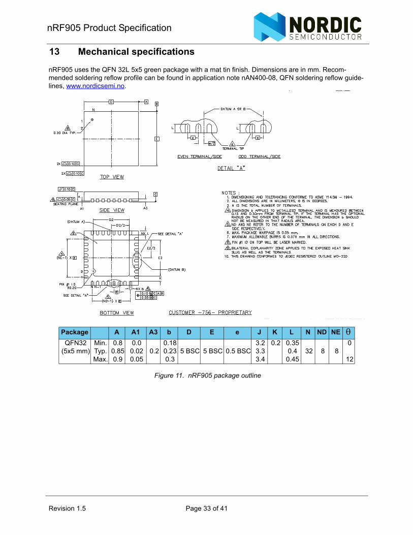
13 Mechanical specifications
nRF905 uses the QFN 32L 5x5 green package with a mat tin finish. Dimensions are in mm. Recom-mended soldering reflow profile can be found in application note nAN400-08, QFN soldering reflow guide-lines, www.nordicsemi.no.
Figure 11. nRF905 package outline
Package A A1 A3 b D E e J K L N ND NE θQFN32
(5x5 mm)Min.Typ.Max.
0.80.850.9
0.00.020.05
0.20.180.230.3
5 BSC 5 BSC 0.5 BSC3.23.33.4
0.2 0.350.40.45
32 8 80
12
Revision 1.5 Page 33 of 41

nRF905 Product Specification
14 Ordering information
14.1 Package marking
14.1.1 Abbreviations
Table 25. Abbreviations
14.2 Product options
14.2.1 RF silicon
Table 26. nRF905 RF silicon options
14.2.2 Development tools
Table 27. nRF905 solution options
n R F B X9 0 5Y Y W W L L
Abbreviation Definition905 Product numberB Build Code, that is, unique code for production sites, package type and, test platform.X "X" grade, that is, Engineering Samples (optional).
YY Two digit Year numberWW Two digit week numberLL Two letter wafer lot number code
Ordering code Package Container MOQa
a. Minimum Order Quantity
nRF905 5x5mm 32-pin QFN, lead free (green)
Tray 490
nRF905-REEL 5x5mm 32-pin QFN, lead free (green)
13” reel 2500
Type Number Description VersionnRF905-EVKIT 433 nRF905 Development kit 433MHz 1.0nRF905-EVKIT 868/915 nRF905 Development kit 868/915MHz 1.0
Revision 1.5 Page 34 of 41

nRF905 Product Specification
15 Application Examples
15.1 Differential Connection to a Loop Antenna
Figure 12. nRF905 Application schematic, differential connection to a loop antenna (433MHz)
Table 28. Recommended external components, differential connection to a loop antenna (433MHz)
Component Description Size Value Tol. UnitsC1 NP0 ceramic chip capacitor, (Crystal oscillator) 0603 22 ±5% pFC2 NP0 ceramic chip capacitor, (Crystal oscillator) 0603 22 ±5% pFC3 NP0 ceramic chip capacitor, (PA supply decoupling) 0603 180 ±5% pFC4 X7R ceramic chip capacitor, (PA supply decoupling) 0603 3.3 ±10% nFC5 NP0 ceramic chip capacitor, (Supply decoupling) 0603 33 ±5% pFC6 X7R ceramic chip capacitor, (Supply decoupling) 0603 4.7 ±10% nFC7 X7R ceramic chip capacitor, (Supply decoupling) 0603 10 ±10% nFC8 NP0 ceramic chip capacitor, (Supply decoupling) 0603 33 ±5% pFC9 NP0 ceramic chip capacitor, (Antenna tuning) 0603 3.9 ±0.1 pFC10 NP0 ceramic chip capacitor, (Antenna tuning) 0603 6.8 ±0.1 pFC11 NP0 ceramic chip capacitor, (Antenna tuning) 0603 4.7 ±0.1 pFC12 NP0 ceramic chip capacitor, (Antenna tuning) 0603 27 ±5% pFC13 NP0 ceramic chip capacitor, (Antenna tuning) 0603 27 ±5% pFR1 0.1W chip resistor, (Crystal oscillator bias) 0603 1 ±5% MΩR2 0.1W chip resistor, (Reference bias) 0603 22 ±1% kΩU1 nRF905 Transceiver QFN32L/5x5X1 Crystal, CL = 12pF LxWxH =
4.0x2.5x0.816 ±60ppm MHz
C222pF0603
C64.7nF0603
C533pF0603
R222K0603
C710nF0603
VDD
C122pF0603
R1
1M
X1
16 MHz
TRX_CE1 VSS 24
VSS 18
VDD 17
VSS
16
PWR_UP2
uPCLK3
VDD4
VSS5
CD6
AM7
DR8
VSS
9
MIS
O10
MO
SI11
SCK
12
XC
215
XC
114
CSN
13
VDD_PA 19ANT1 20ANT2 21VSS 22IREF 23nRF905
VD
D25
VSS
26V
SS27
VSS
28V
SS29
VSS
30D
VD
D_1
V2
31TX
EN32
U1nRF905
VDD
C43.3nF0603
C833pF0603
VDD
TXENTRX_CEPWR_UP
CDAMDR
SPI_MISOSPI_MOSISPI_SCKSPI_CSN
uPCLK
C3180pF
C106.8pF
C114.7pF
aaaaaaaa
J1Loop Antenna, 433MHz35x20mm
C93.9pF
aaaaaaaa
aaaaaaaa
aaaa
aaaa
C1227pF
C1327pF
Revision 1.5 Page 35 of 41

nRF905 Product Specification
15.2 PCB Layout Example; Differential Connection to a Loop Antenna
Figure 13. shows a PCB layout example for the application schematic in Figure 12. A double sided FR-4 board of 1.6mm thickness is used. This PCB has a ground plane on the bottom layer. Additionally, there are ground areas on the component side of the board to ensure sufficient grounding of critical components. A large number of via holes connect the top layer ground areas to the bottom layer ground plane. There is no ground plane beneath the antenna.
Figure 13. PCB layout example for nRF905, differential connection to a loop antenna
A fully qualified RF layout for the nRF905 and its surrounding components, including antennas and match-ing networks, can be downloaded from www.nordicsemi.no.
a) Top silk screen
No components in bottom layer
b) Bottom silk screen
c) Top view d) Bottom view
Revision 1.5 Page 36 of 41
nRF905 Product Specification
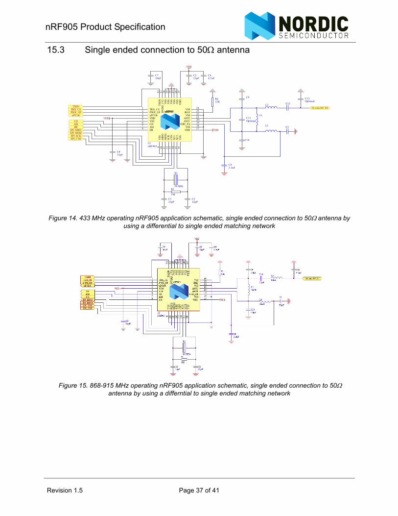
15.3 Single ended connection to 50Ω antenna
Figure 14. 433 MHz operating nRF905 application schematic, single ended connection to 50Ω antenna by using a differential to single ended matching network
Figure 15. 868-915 MHz operating nRF905 application schematic, single ended connection to 50Ω antenna by using a differntial to single ended matching network
C222pF
C64.7nF
C533pF
R222K
C710nF
VDD
C122pF
R1
1M
X1
16 MHz
TRX_CE1 VSS 24
VSS 18
VDD 17
VSS
16
PWR_UP2
uPCLK3
VDD4
VSS5
CD6
AM7
DR8
VSS
9
MIS
O10
MO
SI11
SCK
12
XC
215
XC
114
CSN
13
VDD_PA 19ANT1 20ANT2 21VSS 22IREF 23nRF905
VD
D25
VSS
26V
SS27
VSS
28V
SS29
VSS
30D
VD
D_1
V2
31TX
EN32
U1nRF905
VDD
L1
C3
C11Optional
C12
L3
L2
C9
C10
C43.3nF
C833pF
VDD
C13Optional
C12
C13
L1
L2
L3
33pF, ±5%
Optional
12nH, 5%
12nH, 5%
12nH, 5%
6.8pF, ±5%
Optional
12nH, 5%
39nH, 5%
39nH, 5%
50 ohm RF I/OTXENTRX_CEPWR_UP
CDAMDR
SPI_MISOSPI_MOSISPI_SCKSPI_CSN
uPCLK
aaaaaaaa
aaaaaaaa
aaaa
aaaa
Revision 1.5 Page 37 of 41
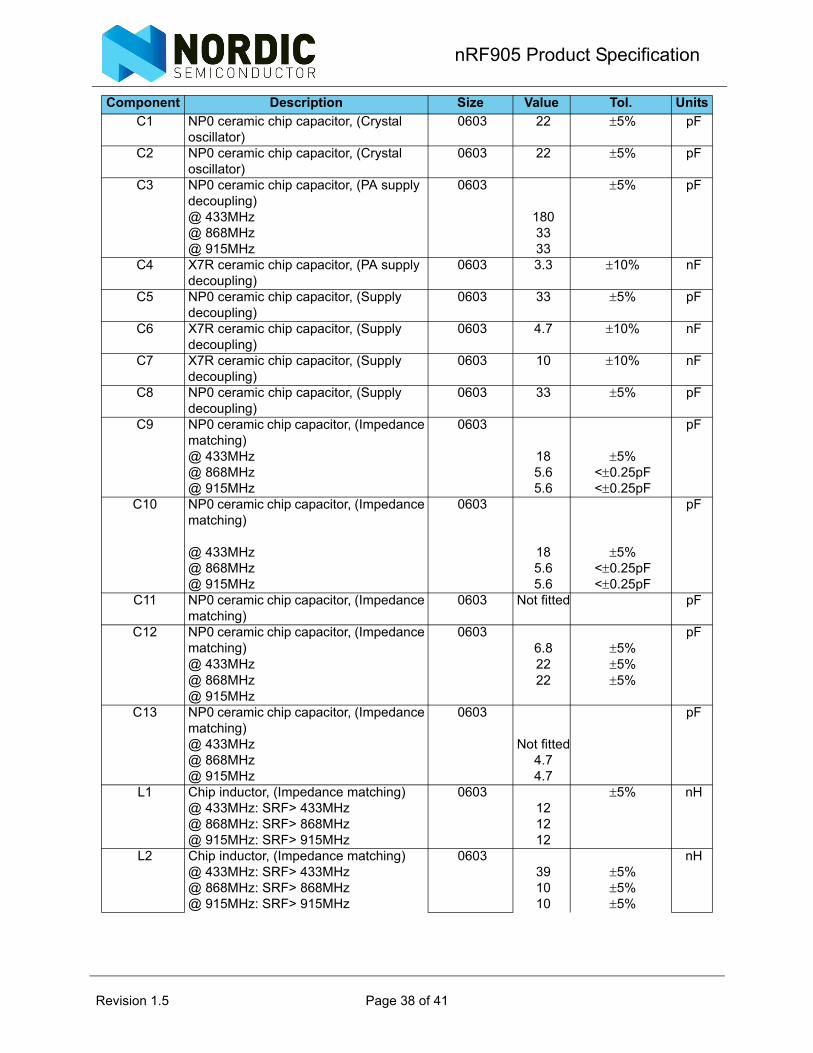
nRF905 Product Specification
Component Description Size Value Tol. UnitsC1 NP0 ceramic chip capacitor, (Crystal
oscillator)0603 22 ±5% pF
C2 NP0 ceramic chip capacitor, (Crystal oscillator)
0603 22 ±5% pF
C3 NP0 ceramic chip capacitor, (PA supply decoupling)
0603 ±5% pF
@ 433MHz 180@ 868MHz 33@ 915MHz 33
C4 X7R ceramic chip capacitor, (PA supply decoupling)
0603 3.3 ±10% nF
C5 NP0 ceramic chip capacitor, (Supply decoupling)
0603 33 ±5% pF
C6 X7R ceramic chip capacitor, (Supply decoupling)
0603 4.7 ±10% nF
C7 X7R ceramic chip capacitor, (Supply decoupling)
0603 10 ±10% nF
C8 NP0 ceramic chip capacitor, (Supply decoupling)
0603 33 ±5% pF
C9 NP0 ceramic chip capacitor, (Impedance matching)
0603 pF
@ 433MHz 18 ±5%@ 868MHz 5.6 <±0.25pF@ 915MHz 5.6 <±0.25pF
C10 NP0 ceramic chip capacitor, (Impedance matching)
0603 pF
@ 433MHz 18 ±5%@ 868MHz 5.6 <±0.25pF@ 915MHz 5.6 <±0.25pF
C11 NP0 ceramic chip capacitor, (Impedance matching)
0603 Not fitted pF
C12 NP0 ceramic chip capacitor, (Impedance matching)@ 433MHz@ 868MHz@ 915MHz
06036.82222
±5%±5%±5%
pF
C13 NP0 ceramic chip capacitor, (Impedance matching)
0603 pF
@ 433MHz Not fitted@ 868MHz 4.7@ 915MHz 4.7
L1 Chip inductor, (Impedance matching) 0603 ±5% nH@ 433MHz: SRF> 433MHz 12@ 868MHz: SRF> 868MHz 12@ 915MHz: SRF> 915MHz 12
L2 Chip inductor, (Impedance matching) 0603 nH@ 433MHz: SRF> 433MHz 39 ±5%@ 868MHz: SRF> 868MHz 10 ±5%@ 915MHz: SRF> 915MHz 10 ±5%
Revision 1.5 Page 38 of 41
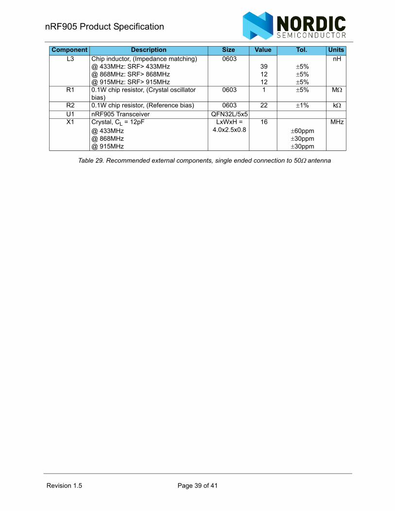
nRF905 Product Specification
Table 29. Recommended external components, single ended connection to 50Ω antenna
L3 Chip inductor, (Impedance matching) 0603 nH@ 433MHz: SRF> 433MHz 39 ±5%@ 868MHz: SRF> 868MHz 12 ±5%@ 915MHz: SRF> 915MHz 12 ±5%
R1 0.1W chip resistor, (Crystal oscillator bias)
0603 1 ±5% MΩ
R2 0.1W chip resistor, (Reference bias) 0603 22 ±1% kΩU1 nRF905 Transceiver QFN32L/5x5X1 Crystal, CL = 12pF LxWxH =
4.0x2.5x0.816 MHz
@ 433MHz ±60ppm@ 868MHz ±30ppm@ 915MHz ±30ppm
Component Description Size Value Tol. Units
Revision 1.5 Page 39 of 41
nRF905 Product Specification
15.4 PCB Layout Example; Single Ended Connection to 50Ω Antenna
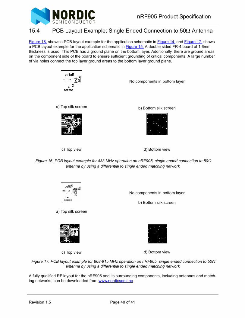
Figure 16. shows a PCB layout example for the application schematic in Figure 14. and Figure 17. shows a PCB layout example for the application schematic in Figure 15. A double sided FR-4 board of 1.6mm thickness is used. This PCB has a ground plane on the bottom layer. Additionally, there are ground areas on the component side of the board to ensure sufficient grounding of critical components. A large number of via holes connect the top layer ground areas to the bottom layer ground plane.
Figure 16. PCB layout example for 433 MHz operation on nRF905, single ended connection to 50Ω antenna by using a differential to single ended matching network
Figure 17. PCB layout example for 868-915 MHz operation on nRF905, single ended connection to 50Ω antenna by using a differential to single ended matching network
A fully qualified RF layout for the nRF905 and its surrounding components, including antennas and match-ing networks, can be downloaded from www.nordicsemi.no
a) Top silk screen
No components in bottom layer
b) Bottom silk screen
c) Top view d) Bottom view
a) Top silk screen
No components in bottom layer
b) Bottom silk screen
c) Top view d) Bottom view
Revision 1.5 Page 40 of 41
nRF905 Product Specification
16 Glossary of terms
Table 30. Glossary of terms.
Term DescriptionADC Analog to Digital ConverterAM Address MatchCD Carrier DetectCLK ClockCRC Cyclic Redundancy CheckDR Data ReadyGFSK Gaussian Frequency Shift KeyingISM Industrial-Scientific-MedicalkSPS kilo Samples per SecondMCU Micro Controller UnitPWR_DWN Power DownPWR_UP Power UpRX ReceiveSPI Serial Programmable Interface CSN SPI Chip Select NotMISO SPI Master In Slave OutMOSI SPI Master Out Slave InSCK SPI Serial ClockSPS Samples per SecondSTBY StandbyTRX_EN Transmit/Receive EnableTX TransmitTX_EN Transmit Enable
Revision 1.5 Page 41 of 41