program studi s1 sistem komputer - core · konsep dasar °memory: akses per ... sinyal high, dan...
TRANSCRIPT

PROGRAM STUDI
S1 SISTEM KOMPUTERUNIVERSITAS DIPONEGORO
Oky Dwi Nurhayati, ST, MTOky Dwi Nurhayati, ST, MTemail: [email protected]: [email protected]
2
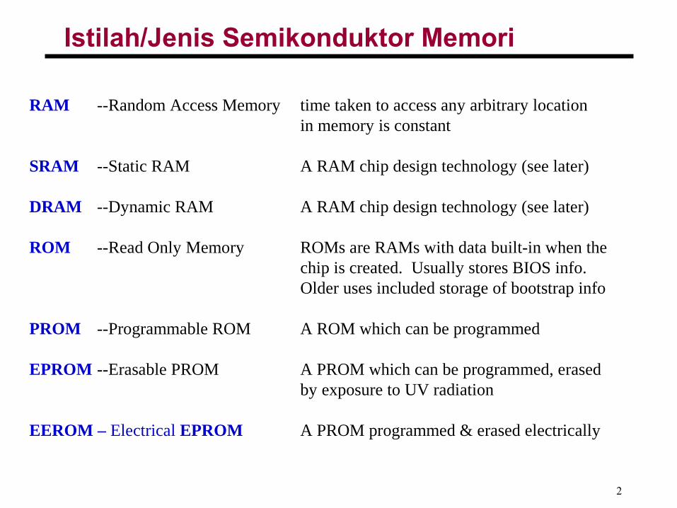
Istilah/Jenis Semikonduktor Memori
RAM --Random Access Memory time taken to access any arbitrary locationin memory is constant
SRAM --Static RAM A RAM chip design technology (see later)
DRAM --Dynamic RAM A RAM chip design technology (see later)
ROM --Read Only Memory ROMs are RAMs with data built-in when thechip is created. Usually stores BIOS info.Older uses included storage of bootstrap info
PROM --Programmable ROM A ROM which can be programmed
EPROM --Erasable PROM A PROM which can be programmed, erasedby exposure to UV radiation
EEROM – Electrical EPROM A PROM programmed & erased electrically
3
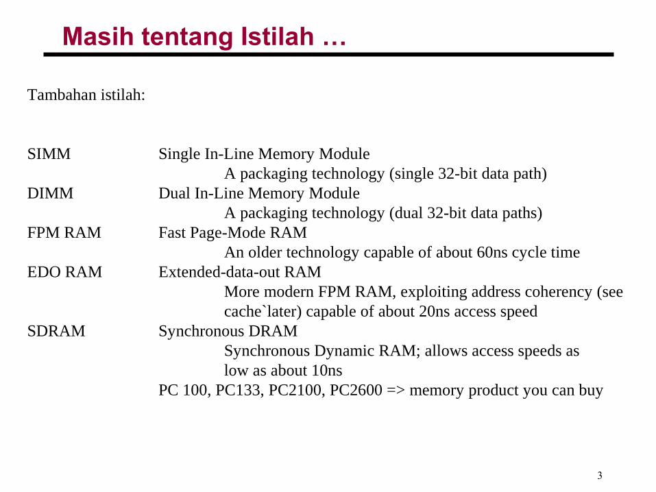
Masih tentang Istilah …
Tambahan istilah:
SIMM Single In-Line Memory ModuleA packaging technology (single 32-bit data path)
DIMM Dual In-Line Memory ModuleA packaging technology (dual 32-bit data paths)
FPM RAM Fast Page-Mode RAMAn older technology capable of about 60ns cycle time
EDO RAM Extended-data-out RAMMore modern FPM RAM, exploiting address coherency (see cache`later) capable of about 20ns access speed
SDRAM Synchronous DRAMSynchronous Dynamic RAM; allows access speeds aslow as about 10ns
PC 100, PC133, PC2100, PC2600 => memory product you can buy

4
Connection: Memory - Processor
MAR
MDR
Processor Memory
Panjang word= n bits
Sampai 2k addressablelocations
k-bit address bus
n-bit data bus
Control lines,R/W, MFC, etc.

5
Konsep Dasar° Memory: akses per byte
• Transfer dilakukan per-word (cepat, kelipatan bytes)
• Misalkan: 32-bit komputer => address 32 bitKemampuan addressing: 2 ^ 32 = 4 Gbytes
• Jika transfer data per-word: 32 bit (data bus) => 4 bytes
• Bytes mana yang diakses dari kemungkinan word tsb?
- Perlu 2 bits untuk menentukan bytes yang mana dari word
- Sisa bit: 30 bits digunakan untuk address word

6
Organisasi Internal Memori° Bentuk array: terdiri dari sel memori
• Sel berisi 1 bit informasi• Baris dari sel membentuk untaian satu word• Contoh: 16 x 8 memori
- memori SRAM mengandung 16 words- setiap words terdiri dari 8 bit data- Kapasitas memori: 16 x 8 = 128 bits
• Decoder digunakan untuk memilih baris word mana yang akan diakses
- Tipikal SRAM, array 1 dimensi => indeks dari baris pada array tersebut.

7
Organisasi Memori: 1-level-decode SRAM (128 x 8)
Addressdecoder
A0
A1
A6
sense/writeamps
b7’b7
d7
sense/writeamps
b1’b1
d1
sense/writeamps
b0’b0
d0Input/output lines
W0
W1
W127
memorycells
R/W’
Word 8 bit data
128 words
CS
8
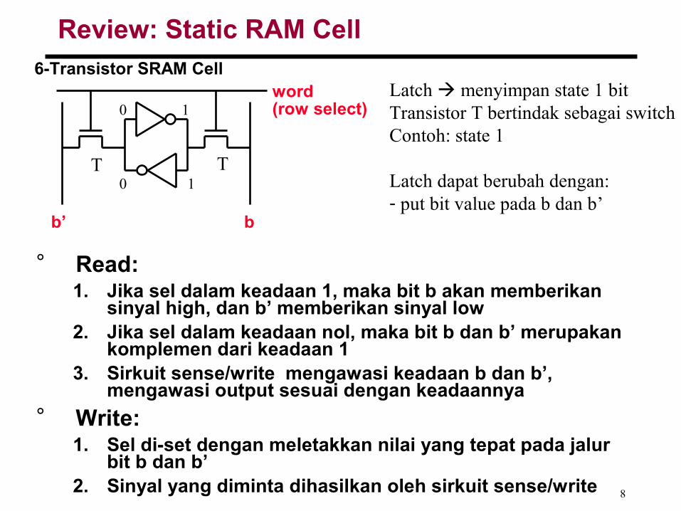
Review: Static RAM Cell6-Transistor SRAM Cell
b’ b
word(row select)
° Read:1. Jika sel dalam keadaan 1, maka bit b akan memberikan
sinyal high, dan b’ memberikan sinyal low2. Jika sel dalam keadaan nol, maka bit b dan b’ merupakan
komplemen dari keadaan 13. Sirkuit sense/write mengawasi keadaan b dan b’,
mengawasi output sesuai dengan keadaannya° Write:
1. Sel di-set dengan meletakkan nilai yang tepat pada jalur bit b dan b’
2. Sinyal yang diminta dihasilkan oleh sirkuit sense/write
10
0 1
T T
Latch menyimpan state 1 bitTransistor T bertindak sebagai switchContoh: state 1
Latch dapat berubah dengan:- put bit value pada b dan b’
9
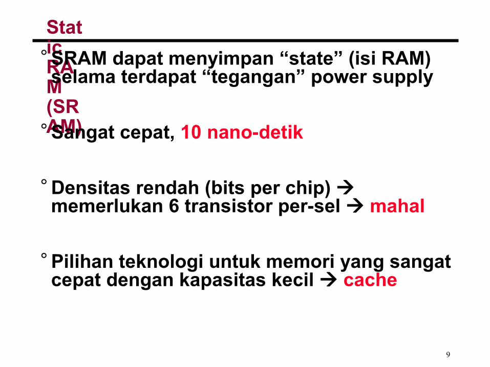
Static RAM (SRAM)
° SRAM dapat menyimpan “state” (isi RAM) selama terdapat “tegangan” power supply
° Sangat cepat, 10 nano-detik
° Densitas rendah (bits per chip) memerlukan 6 transistor per-sel mahal
° Pilihan teknologi untuk memori yang sangat cepat dengan kapasitas kecil cache

10
Organisasi Memori: 2-level-decode SRAM (1 K x 1)
5-bitdecoder
W0W1
W31
32 x 32 Memory cell array
32 x 1Output/input multiplexer
Sense/write circuitry
R/W
CS
5-bit column address
5-bit row address
10-bit addressData Input/Output (1 bit)
A0
A1
A7
A8
A9
11
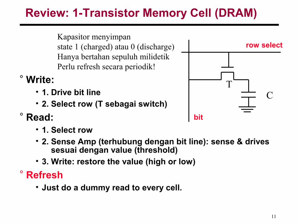
Review: 1-Transistor Memory Cell (DRAM)
° Write:• 1. Drive bit line• 2. Select row (T sebagai switch)
° Read:• 1. Select row• 2. Sense Amp (terhubung dengan bit line): sense & drives
sesuai dengan value (threshold)• 3. Write: restore the value (high or low)
° Refresh• Just do a dummy read to every cell.
row select
bit
TC
Kapasitor menyimpan state 1 (charged) atau 0 (discharge)Hanya bertahan sepuluh milidetikPerlu refresh secara periodik!
12
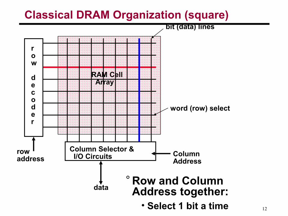
Classical DRAM Organization (square)
row
decoder
rowaddress
Column Selector & I/O Circuits Column
Address
data
RAM Cell Array
word (row) select
bit (data) lines
° Row and Column Address together:
• Select 1 bit a time

13
Dynamic RAM (DRAM)° Slower than SRAM
• access time ~60 ns (paling cepat: 35 ns)° Nonpersistent
• every row must be accessed every ~1 ms (refreshed)
° Densitas tinggi: 1 transistor/bit • Lebih murah dari SRAM • ~$1/MByte [2002]
° Pilihan teknologi memori untuk kapasitas besar dan “low cost” main memory

14
Organisasi DRAM 2-level (64Kx1)
Rowaddress
latch
Columnaddress
latch
Row decoder 256x256
cell array
columnsense/write
amps
columndecoder
A15-A8/A7-A0
\8
\8
R/W’
Dout DinCAS’
RAS’
row
col
256 Rows
256 Columns
CS
15
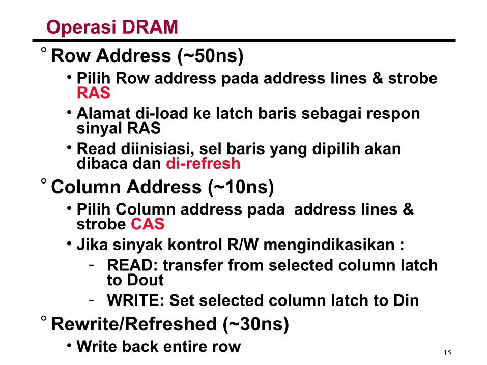
Operasi DRAM° Row Address (~50ns)
• Pilih Row address pada address lines & strobe RAS
• Alamat di-load ke latch baris sebagai respon sinyal RAS
• Read diinisiasi, sel baris yang dipilih akan dibaca dan di-refresh
° Column Address (~10ns)• Pilih Column address pada address lines &
strobe CAS• Jika sinyak kontrol R/W mengindikasikan :
- READ: transfer from selected column latch to Dout
- WRITE: Set selected column latch to Din° Rewrite/Refreshed (~30ns)
• Write back entire row
16
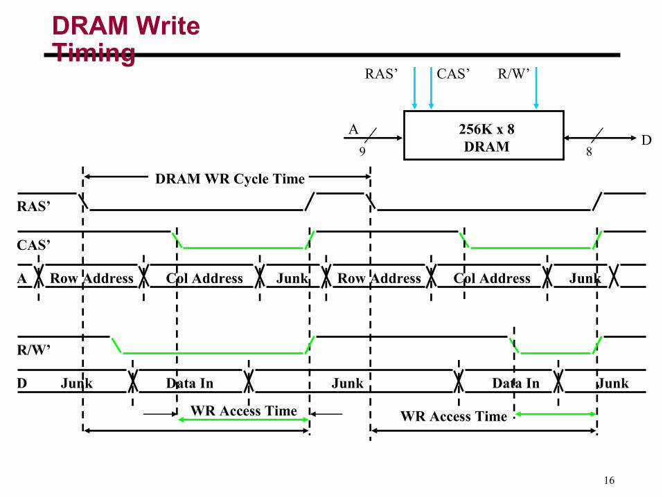
DRAM Write Timing
AD
256K x 8DRAM9 8
R/W’CAS’RAS’
R/W’
A Row Address Junk
CAS’
RAS’
Col Address Row Address JunkCol Address
D Junk JunkData In Data In Junk
DRAM WR Cycle Time
WR Access Time WR Access Time

17
DRAM Read Timing
AD
256K x 8DRAM9 8
R/W’CAS’RAS’
R/W’
A Row Address Junk
CAS’
RAS’
Col Address Row Address JunkCol Address
D High Z Data Out
DRAM Read Cycle Time
Junk Data Out High ZRead Access
TimeRead Access
Time

18
DRAM: Kinerja° Timing
• Access time = 60ns < cycle time = 90ns• Need to rewrite row• Model asinkron: operasi memori dilakukan oleh
controller circuit delayprosesor menunggu sampai cycle time selesai lalu melakukan request lagi.
° Must Refresh Periodically• Perform complete memory cycle for each row• Approx. every 1ms• Handled in background by memory controller

19
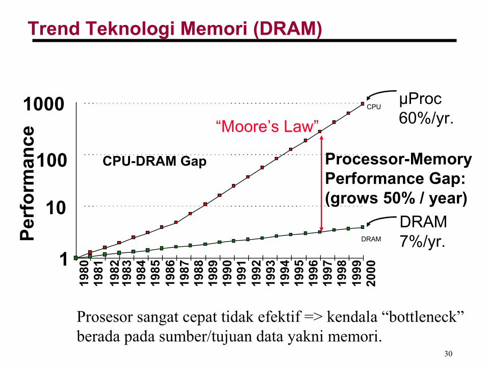
Perkembangan Teknologi Memori DRAM° Teknologi memori: segi kecepatan akses
berkembang sangat lambat• Gap yang semakin membesar dengan
kecepatan prosesor (cycle sangat kecil => 1 nsec, akses memori orde puluhan nsec).
° Perkembangan teknologi DRAM• Basis tetap sama: 1-transistor memori cell
(menggunakan kapasitor)• Inovasi dilakukan dari segi: cara melakukan
akses- memotong waktu akses (mis. CAS tidak
diperlukan)- burst mode: sekaligus mengambil data
sebanyak mungkin (seluruh word)- perlu tambahan rangkaian: register, latch dll

20
Enhanced Performance DRAMs
° Conventional Access• Row + Col• RAS CAS RAS CAS ...
° Page Mode• Row + Series of columns• RAS CAS CAS CAS ...• Gives successive bits
° Video RAM• Shift out entire row sequentially• At video rate
Rowaddress
latch
Columnaddress
latch
Row decoder 256x256
cell array
sense/writeamps
columndecoder& latch
A15-A8/A7-A0
\8
\8
R/W’
CAS
RAS
row
col
Entire row buffered here
row access time col access time cycle time page mode cycle time 50ns 10ns 90ns 25ns
Typical Performance

21
Fast Page Mode Operation
° Fast Page Mode DRAM• N x M “SRAM” to save a row
° After a row is read into the register
• Only CAS is needed to access other M-bit blocks on that row
• RAS’ remains asserted while CAS’ is toggled
A Row Address
CAS’
RAS’
Col Address Col Address
1st M-bit Access
N ro
ws
N cols
DRAM
ColumnAddress
M-bit OutputM bits
N x M “SRAM”
RowAddress
Col Address Col Address
2nd M-bit 3rd M-bit 4th M-bit
22
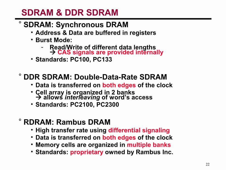
SDRAM & DDR SDRAM° SDRAM: Synchronous DRAM
• Address & Data are buffered in registers• Burst Mode:
- Read/Write of different data lengths CAS signals are provided internally
• Standards: PC100, PC133
° DDR SDRAM: Double-Data-Rate SDRAM• Data is transferred on both edges of the clock• Cell array is organized in 2 banks allows interleaving of word’s access
• Standards: PC2100, PC2300
° RDRAM: Rambus DRAM• High transfer rate using differential signaling• Data is transferred on both edges of the clock• Memory cells are organized in multiple banks• Standards: proprietary owned by Rambus Inc.
23
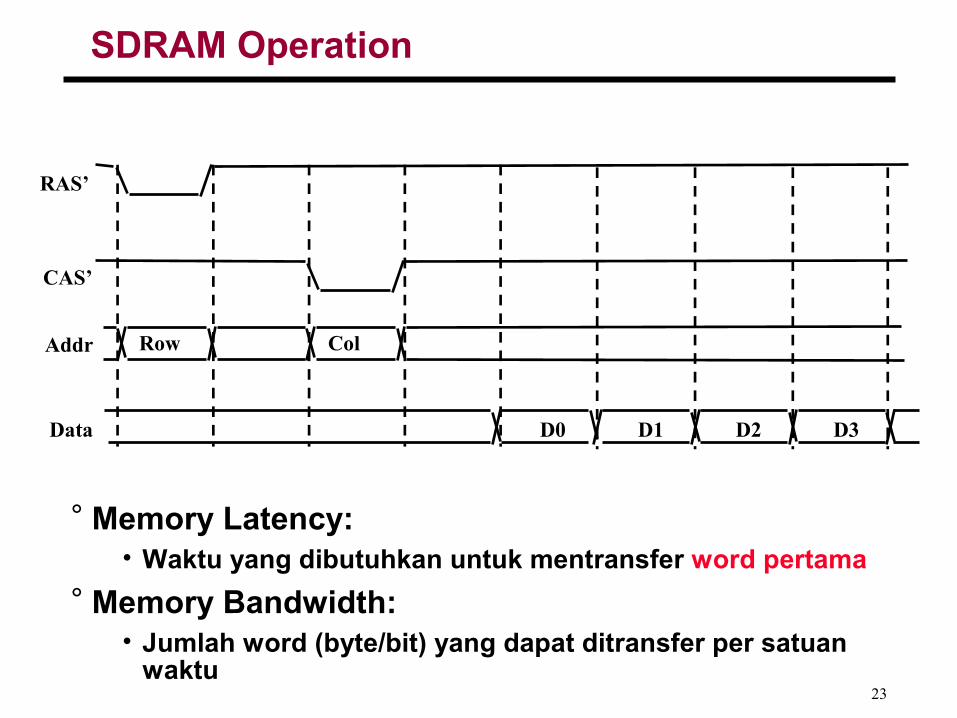
SDRAM Operation
Data
CAS’
D0 D1 D2 D3
Row Col
RAS’
Addr
° Memory Latency:• Waktu yang dibutuhkan untuk mentransfer word pertama
° Memory Bandwidth:• Jumlah word (byte/bit) yang dapat ditransfer per satuan
waktu
24
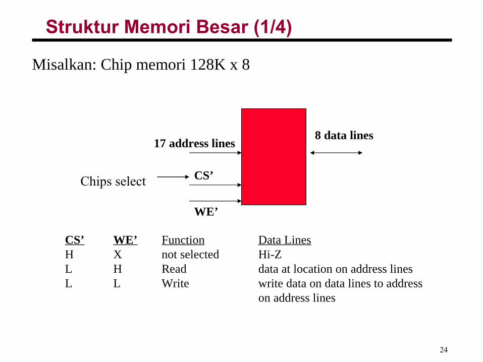
Struktur Memori Besar (1/4)
Misalkan: Chip memori 128K x 8
17 address lines8 data lines
CS’
WE’
CS’ WE’ Function Data LinesH X not selected Hi-ZL H Read data at location on address linesL L Write write data on data lines to address
on address lines
Chips select

25
Contoh: Struktur 1 MB (2/4)
1 MB dapat dikonstruksi dengan organisasi 8 chips memori 128 KB (8 x 128 x 8 = 1 MB)
The address space ispartitioned into 128Kblocks;
block 0 has addresses 0 -- 128K -1block 1 has addresses 128K -- 256K-1block 2 has addresses 256K -- 384K -1::::block 7 has addresses 896K -- 1024K -1
This will be chip 0
This will be chip 1
This will be chip 7
Berapa banyak bits yang diperlukan untuk alamat pada chips? memilih chips yang mana?

26
Contoh: Pembagian field address (3/4)
1MB membutuhkan alamat sebesar 20 bit, Ide: membagi field address menjadi 2 yakni: bits untuk memilih chips dan address pada field tsb.
Bits 16 -- 0 (17 address bits)Bits 19 -- 17 (3 address bits)
17 bits select the address in each128KB block (== each chip)
3 address bits select on of the 8128KB blocks (chips)

27
Contoh: Struktur 1MB memory (4/4)
3-to-8decoder
20 Address Lines
17 Address Lines A16 -- A0
3 Address Lines A19--A17
Write
/WE
Data Lines
28
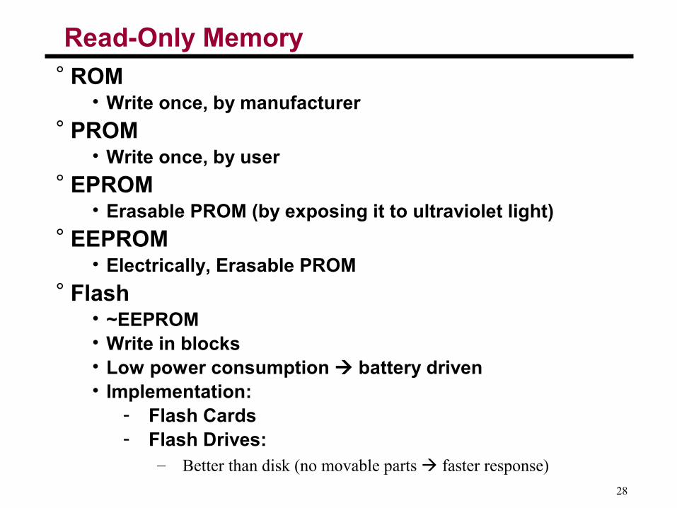
Read-Only Memory° ROM
• Write once, by manufacturer° PROM
• Write once, by user° EPROM
• Erasable PROM (by exposing it to ultraviolet light)° EEPROM
• Electrically, Erasable PROM° Flash
• ~EEPROM• Write in blocks• Low power consumption battery driven• Implementation:
- Flash Cards- Flash Drives:
– Better than disk (no movable parts faster response)
29
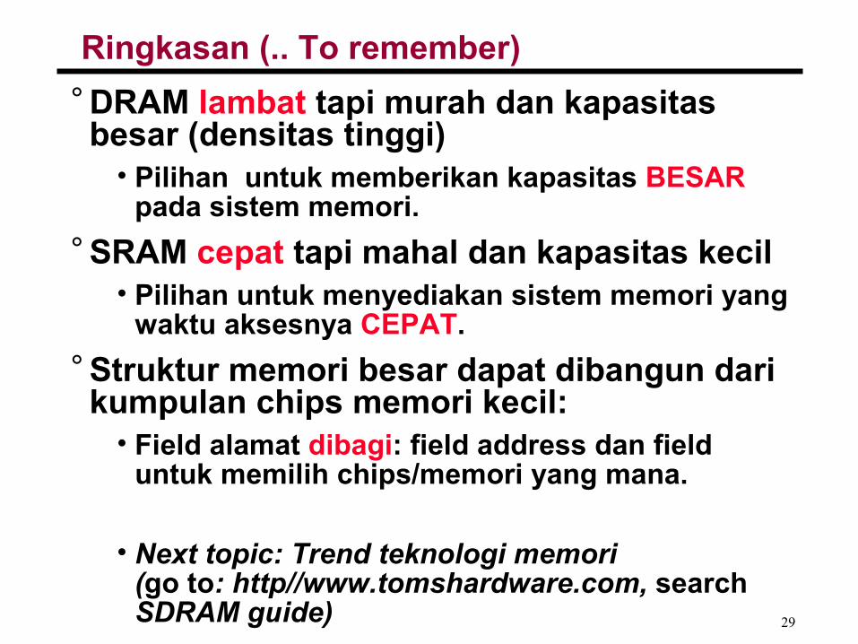
Ringkasan (.. To remember)° DRAM lambat tapi murah dan kapasitas
besar (densitas tinggi)• Pilihan untuk memberikan kapasitas BESAR
pada sistem memori.° SRAM cepat tapi mahal dan kapasitas kecil
• Pilihan untuk menyediakan sistem memori yang waktu aksesnya CEPAT.
° Struktur memori besar dapat dibangun dari kumpulan chips memori kecil:
• Field alamat dibagi: field address dan field untuk memilih chips/memori yang mana.
• Next topic: Trend teknologi memori (go to: http//www.tomshardware.com, search SDRAM guide)
30
Trend Teknologi Memori (DRAM)
CPU-DRAM Gap
µProc60%/yr.
DRAM7%/yr.
1
10
100
100019
8019
81
1983
1984
1985
1986
1987
1988
1989
1990
1991
1992
1993
1994
1995
1996
1997
1998
1999
2000
DRAM
CPU19
82
Processor-MemoryPerformance Gap:(grows 50% / year)
Perf
orm
ance
“Moore’s Law”
Prosesor sangat cepat tidak efektif => kendala “bottleneck”berada pada sumber/tujuan data yakni memori.