programmable logic design for an optical access network · fpga field programmable gate array fsan...
TRANSCRIPT
HELSINKI UNIVERSITY OF TECHNOLOGY
Department of Electrical and Communications Engineering
SAMI LALLUKKA
Programmable logic design for an optical access network
Thesis submitted in partial fulfillment of the requirements for the degree ofMaster of Science in Technology
Espoo 27th May 2003
Supervisor: Professor (pro tem) Samuli Aalto, HUTInstructor: Lic.Sc. (Tech.) Kari Seppänen, VTT
Abstract
HELSINKI UNIVERSITY OF TECHNOLOGY ABSTRACT OF THEMASTER’ S THESIS
Author: Sami LallukkaName of the Thesis: Programmable logic design for an optical access networkDate: 27th May 2003 Number of pages: 99
Department: Department of Electrical and Communications EngineeringProfessorship: S-38
Supervisor: Professor (pro tem) Samuli AaltoInstructor: Lic.Sc. (Tech.) Kari Seppänen
The structure of communication networks is going to change in the future. Data-com, telecom and broadcast traffic is conventionally transported over separatednetworks, which is a major cost factor in network management for operators. Inaddition, legacy communication networks cannot provide adequate quality of ser-vice for the emerging interactive multimedia services. For this reason, the devel-opment of communications networks is heading towards flexibility and conver-gence.
At the moment, the bottleneck factor in the development of communication net-works transfer speed is the complexity of the metropolitan area feeder networks.This has a considerable effect on the service quality in this area as well. TheTEKES-funded OAN-project concentrates on developing a new and simpler met-ropolitan optical feeder network, which could be used to improve the quality ofservice in the metropolitan area.
This thesis has been prepared as a part of the OAN-project. In this thesis, thestructure of the present communication networks is presented and its problemsare discussed. Based on this discussion, the future structure of communicationnetworks is illustrated. Furthermore, the HDL-implementation process with itsaggregates will be discussed. Finally, a programmable logic design for the op-tical metropolitan feeder network prototype, implemented in the OAN project, ispresented.
Keywords: FPGA, VHDL, DoS, optical feeder network
i
Tiivistelmä
TEKNILLINEN KORKEAKOULU DIPLOMITYÖN TIIVISTELMÄ
Nimi: Sami LallukkaTyön nimi: Optisen liityntäverkon ohjelmoitavien logiikkapiirien ohjelmoinnin
suunnitteluPäivämäärä: 27. toukokuuta 2003 Sivumäärä: 99
Osasto: Sähkö- ja tietoliikennetekniikan osastoLaboratorio: S-38
Valvoja: Professori (ma.) Samuli AaltoOhjaaja: TkL. Kari Seppänen
Tiedonsiirtoverkkojen rakenne elää muutoksen aikaa. Perinteisesti data-, puhelin-ja laajakaistaliikenne on siirretty erillisissä verkoissa, joiden samanaikainen yl-läpitäminen tuottaa ylimääräisiä kustannuksia operaattoreille. Lisäksi uudet in-teraktiiviset palvelut vaativat toimiakseen sellaista palvelunlaatua, jota nykyisettiedonsiirtoverkot eivät kykene tarjoamaan. Näiden epäkohtien johdosta tiedon-siirtoverkkojen kehityksessä tähdätään uusiin, entistä joustavampiin ja eri toimin-not yhdistäviin verkkoratkaisuihin, joissa tiedonsiirron palvelunlaadulla on entistäsuurempi merkitys.
Tällä hetkellä tiedonsiirtoverkkojen kokonaistiedonsiirtonopeuden kasvun pul-lonkaulatekijäksi on muodostunut kaupunkialueiden syöttöverkkojen monimut-kaisuus, millä on suuri vaikutus myös tiedonsiirron palvelunlaatuun. TEKES-rahoitteisessa OAN-projektissa kehitetään uutta ja yksinkertaisempaa kaupunkia-lueen optista syöttöverkkoratkaisua, jolla alueen palvelunlaatua saataisiin paran-nettua.
Tämä diplomityö on tehty osana OAN-projektia. Työssä kuvataan tiedonsiir-toverkkojen tämänhetkinen rakenne, tarkastellaan sen ongelmia ja tulevaisuu-den kehityssuuntia, sekä esitetään pohdintojen pohjalta rakennettu malli tu-levaisuuden tiedonsiirtoverkkojen rakenteelle. Työssä esitetään myös HDL-implementointiprosessiin kuuluvat työvaiheet sekä käydään läpi suunnitelmaOAN-projektissa toteutettavan prototyypin ohjelmoitavien logiikkapiirien ohjel-maa varten.
Avainsanat: FPGA, VHDL, DoS, optinen syöttöverkko
ii
Foreword
This thesis has been written in partial fulfillment of the requirements for the de-gree of Master of Science in Technology while participating in the OAN researchproject at VTT Information Technology, Broadband Communications.
On behalf of the employer, I would like to thank Markku Sipilä and KristiinaHytönen for the possibility to write this thesis at VTT. Furthermore, I would liketo thank all of my colleagues for their support and advice during the writing pro-cess; in particular, Kari Seppänen for his excellent ideas, guidance and proof read-ing; also, Risto Mutanen and Juha Zidbeck for their valuable advice and insights.Most of all, I would like to thank all of the VTT personnel located in the samepremises for a splended atmosphere, especially, the gang in the coffee and lunchbreaks. Finally, special thanks to my supervisor, Samuli Aalto at Helsinki Univer-sity of Technology for excellent cooperation, careful proof reading and guidance.
I would also like to thank all of my family, relatives and friends, who have motiv-ated me in my studies.
27th May 2003, Espoo, Finland
Sami Lallukka
iii
Contents
Abstract i
Tiivistelmä ii
Foreword iii
Table of contents vi
Acronyms vii
List of pictures xiii
List of tables xiv
1 Introduction 11.1 Motivation . . . . . . . . . . . . . . . . . . . . . . . . . . . . . . 21.2 Goal . . . . . . . . . . . . . . . . . . . . . . . . . . . . . . . . . 21.3 Structure . . . . . . . . . . . . . . . . . . . . . . . . . . . . . . . 2
2 Communication networks today 32.1 Access network . . . . . . . . . . . . . . . . . . . . . . . . . . . 4
2.1.1 Distribution networks . . . . . . . . . . . . . . . . . . . . 62.1.2 Feeder networks . . . . . . . . . . . . . . . . . . . . . . 9
2.2 Transport networks . . . . . . . . . . . . . . . . . . . . . . . . . 122.2.1 Data centric services . . . . . . . . . . . . . . . . . . . . 122.2.2 Synchronisation . . . . . . . . . . . . . . . . . . . . . . 13
2.3 Network topologies . . . . . . . . . . . . . . . . . . . . . . . . . 142.4 Optical Networks . . . . . . . . . . . . . . . . . . . . . . . . . . 15
2.4.1 Synchronous Digital Hierarchy (SDH) . . . . . . . . . . . 162.4.2 Wavelength Division Multiplexing (WDM) . . . . . . . . 182.4.3 Optical Transport Network (OTN) . . . . . . . . . . . . . 20
2.5 Survivability . . . . . . . . . . . . . . . . . . . . . . . . . . . . . 21
iv
CONTENTS
3 Communication networks tomorrow 233.1 Future characteristics . . . . . . . . . . . . . . . . . . . . . . . . 24
3.1.1 Distribution networks . . . . . . . . . . . . . . . . . . . . 263.1.2 Metropolitan area networks . . . . . . . . . . . . . . . . 273.1.3 Transport networks . . . . . . . . . . . . . . . . . . . . . 283.1.4 Optical networks . . . . . . . . . . . . . . . . . . . . . . 29
3.2 Future technologies . . . . . . . . . . . . . . . . . . . . . . . . . 293.2.1 Passive optical networks (PONs) . . . . . . . . . . . . . . 293.2.2 Resilient Packet Ring (RPR) . . . . . . . . . . . . . . . . 323.2.3 Data over SDH (DoS) . . . . . . . . . . . . . . . . . . . 33
3.3 Recent research projects . . . . . . . . . . . . . . . . . . . . . . 363.3.1 HARMONICS . . . . . . . . . . . . . . . . . . . . . . . 363.3.2 IP-HORNET . . . . . . . . . . . . . . . . . . . . . . . . 383.3.3 DAVID . . . . . . . . . . . . . . . . . . . . . . . . . . . 393.3.4 Discussion . . . . . . . . . . . . . . . . . . . . . . . . . 40
4 Research project OAN 414.1 OAN test network architecture . . . . . . . . . . . . . . . . . . . 414.2 OAN test network prototype . . . . . . . . . . . . . . . . . . . . 43
4.2.1 Functionality of the node . . . . . . . . . . . . . . . . . . 444.2.2 Network structure . . . . . . . . . . . . . . . . . . . . . . 45
5 FPGA programming methodology 475.1 FPGA basics . . . . . . . . . . . . . . . . . . . . . . . . . . . . 475.2 HDL-implementation process . . . . . . . . . . . . . . . . . . . . 49
5.2.1 Design planning . . . . . . . . . . . . . . . . . . . . . . 495.2.2 Design flow . . . . . . . . . . . . . . . . . . . . . . . . . 495.2.3 Verification . . . . . . . . . . . . . . . . . . . . . . . . . 50
5.3 Design guidelines . . . . . . . . . . . . . . . . . . . . . . . . . . 515.4 Design quality . . . . . . . . . . . . . . . . . . . . . . . . . . . . 52
6 HDL-design options 536.1 Target architectures . . . . . . . . . . . . . . . . . . . . . . . . . 536.2 Programming tools . . . . . . . . . . . . . . . . . . . . . . . . . 556.3 Design options . . . . . . . . . . . . . . . . . . . . . . . . . . . 55
6.3.1 Control functions . . . . . . . . . . . . . . . . . . . . . . 566.3.2 Network functions . . . . . . . . . . . . . . . . . . . . . 58
7 HDL Design 627.1 Design functionality . . . . . . . . . . . . . . . . . . . . . . . . . 627.2 Distribution of clocks . . . . . . . . . . . . . . . . . . . . . . . . 63
v

CONTENTS
7.3 Control part . . . . . . . . . . . . . . . . . . . . . . . . . . . . . 677.3.1 Registers . . . . . . . . . . . . . . . . . . . . . . . . . . 677.3.2 Accessing the interface card registers . . . . . . . . . . . 697.3.3 Clock controller . . . . . . . . . . . . . . . . . . . . . . 707.3.4 PCI interface . . . . . . . . . . . . . . . . . . . . . . . . 717.3.5 Router control . . . . . . . . . . . . . . . . . . . . . . . 727.3.6 I/O control . . . . . . . . . . . . . . . . . . . . . . . . . 737.3.7 Control line . . . . . . . . . . . . . . . . . . . . . . . . . 737.3.8 Microprocessor interface . . . . . . . . . . . . . . . . . . 747.3.9 SRAM interface . . . . . . . . . . . . . . . . . . . . . . 757.3.10 Laser controller . . . . . . . . . . . . . . . . . . . . . . . 75
7.4 Network part . . . . . . . . . . . . . . . . . . . . . . . . . . . . 777.4.1 POS-PHY level 3 . . . . . . . . . . . . . . . . . . . . . . 777.4.2 FIFO controller . . . . . . . . . . . . . . . . . . . . . . . 797.4.3 POS-PHY Level 4 . . . . . . . . . . . . . . . . . . . . . 807.4.4 Gb Ethernet (GbE) packet scheduler . . . . . . . . . . . . 817.4.5 POS packet scheduler . . . . . . . . . . . . . . . . . . . 817.4.6 GFP framing and deframing . . . . . . . . . . . . . . . . 827.4.7 VC and LCAS . . . . . . . . . . . . . . . . . . . . . . . 837.4.8 SDH framing . . . . . . . . . . . . . . . . . . . . . . . . 857.4.9 APS . . . . . . . . . . . . . . . . . . . . . . . . . . . . . 857.4.10 Parallel TelecomBus interface . . . . . . . . . . . . . . . 867.4.11 Preliminary TelecomBus interface . . . . . . . . . . . . . 87
8 Conclusions 898.1 Results . . . . . . . . . . . . . . . . . . . . . . . . . . . . . . . . 898.2 Future developments . . . . . . . . . . . . . . . . . . . . . . . . 90
Bibliography 92
vi
Acronyms
ADM Add Drop Multiplexer
AN Access Node
APON ATM Passive Optical Network
APS Automatic Protection Switching
ASIC Application Specific Integrated Circuit
ASON Automatically Switched Optical Network
ASTN Automatically Switched Transport Network
ATM Asynchronous Transfer Mode
AWG Arrayed Waveguide Gratings
BER Bit Error Rate
BPON Broadband PON
CATV Cable Antenna Television
CLB Configurable Logic Block
CO Central Office
CPU Central Processing Unit
CRC Cyclic Redundancy Check
DCM Digital Clock Manager
DIP Diagonal Interleaved Parity
DLL Delay Locked Loop
vii
DWDM Dense Wavelength Division Multiplexing
DoS Data over SDH
EFM Ethernet in the First Mile
EPON Ethernet PON
FDM Frequency Division Multiplexing
FEC Forward Error Correction
FIFO First In First Out memory
FPGA Field Programmable Gate Array
FSAN Full Service Access Networks
FTTx Fiber-to-the-x, where x stands for C (Curb), B (Building) or H (Home).
GFP-F Frame-mapped GFP
GFP-T Transparent GFP
GFP Generic Framing Procedure
GMPLS Generic MPLS
GPON Gb PON
GSM Global System for Mobile communication
HDLC High level Data Link Control
HDL Hardware Description Language
HEC Header Error Checksum
HUT Helsinki University of Technology
IEEE Institute of Electrical and Electronics Engineers
IOB Input/Output Block
IPsec IP Security
IP Internet Protocol
ISDN Integrated Services Digital Network
viii
IST Information Society Technologies
ITU-T International Telecommunication Union, Telecommunication standard-isation sector
IWF Interworking Functions
LAN Local Area Network
LCAS Link Capacity Adjustment Scheme
LED Light Emitting Diode
LVDS Low Voltage Differential Signalling
MAC Medium Access Control
MAN Metropolitan Area Network
MPLS Multi Protocol Label Switching
N-ISDN Narrow-band ISDN
OAN Optical Access Networking
OLT Optical Line Terminal
OLT Optical Line Termination
ONT Optical Network Terminal
ONU Optical Network Unit
OPADM Optical Packet Add/Drop Multiplexer
OPR Optical Packet Router
OSI Open Systems Interconnection
OTN Optical Transport Network
OXC Optical Cross Connect
PCI Peripheral Component Interconnect
PDH Plesiochronic Digital Hierarchy
PHY Physical Layer
ix

PLL Phase Locked Loop
POH Path Overhead
PON Passive Optical Network
POS Packet Over SDH
POTS Plain Old Telephone Service
PPP Point-to-Point Protocol
PSTN Public Switched Telephone Network
QoS Quality of Service
RAM Random Access Memory
RPR Resilient Packet Ring
SAN Storage Area Network
SDH Synchronous Digital Hierarchy
SNMP Simple Network Management Protocol
SONET Synchronous Optical Network
SRAM Static Random Access Memory
STM-1 Synchronous Transport Module 1
T1X1 Standards Committee T1 Telecommunications, Technical Subcommitteeof Digital Hierarchy and Synchronization
TBS TelecomBus Serialiser
TDMA Time Division Multiple Access
TDM Time Division Multiplexing
TEKES National technology agency
TOH Transport Overhead
VCG Virtual Concatenation Group
VC Virtual Concatenation
x
VHDL VHSIC Hardware Description Language
VHSIC Very High Speed Integrated Circuit
VPN Virtual Private Network
VTT Technical Research Centre of Finland
VoIP Voice over IP
WADM Wavelength Add Drop Multiplexer
WAN Wide Area Network
WDMA Wavelength Division Multiple Access
WDM Wavelength Division Multiplexing
xDSL x-Digital Subscriber Line
xi
List of Figures
2.1 The overlaid structure of communication networks. . . . . . . . . 52.2 The definition of access network. . . . . . . . . . . . . . . . . . . 62.3 Access technologies in today’s networks. . . . . . . . . . . . . . 72.4 MAN traffic characteristics today. . . . . . . . . . . . . . . . . . 92.5 The definition of transport network. . . . . . . . . . . . . . . . . 112.6 Topologies used in networks today. . . . . . . . . . . . . . . . . . 142.7 Traffic grooming in WDM networks. . . . . . . . . . . . . . . . . 19
3.1 The structure of the future communication network. . . . . . . . . 253.2 The architecture and principle of TDMA and WDMA PONs . . . 303.3 Protection mechanisms in RPR. . . . . . . . . . . . . . . . . . . 333.4 Functional model of GFP . . . . . . . . . . . . . . . . . . . . . . 343.5 The protocol stack of the GFP . . . . . . . . . . . . . . . . . . . 343.6 The architecture of the HARMONICS project . . . . . . . . . . . 373.7 The architecture of the IP-HORNET project . . . . . . . . . . . . 383.8 The outline of the DAVID project demonstrator . . . . . . . . . . 40
4.1 The network layer protocol stack of the OAN test network. . . . . 424.2 Simplified architecture of the OAN test network prototype node. . 444.3 The network structure and data transmission process in the OAN
test network prototype. . . . . . . . . . . . . . . . . . . . . . . . 46
5.1 The basic structure of the FPGA-chip. . . . . . . . . . . . . . . . 485.2 The HDL design flow according to Xilinx . . . . . . . . . . . . . 505.3 Verification as a part of design implementation process . . . . . . 51
6.1 Virtex-II FPGA structure, adopted from [Inc00c]. . . . . . . . . . 546.2 The formation of the control functions in the OAN prototype. . . . 576.3 The overall functionality of the OAN network. . . . . . . . . . . . 586.4 The overall functionality of the OAN network ring operations. . . 60
7.1 The functionality of the FPGAs in the OAN prototype. . . . . . . 64
xii
LIST OF FIGURES
7.2 The block design for the larger FPGA in the OAN prototype. . . . 657.3 The block designs for the smaller FPGA in the router card (a) and
for the FPGA in the interface-card (b). . . . . . . . . . . . . . . . 657.4 The sources of clocks in the OAN prototype. . . . . . . . . . . . . 667.5 The clock domains in the OAN HDL design. . . . . . . . . . . . . 687.6 The HW implementation of a bitwise CRC operation. . . . . . . . 747.7 The composition of the data transported over control line. . . . . . 747.8 The signals in POS-PHY level 3 interface . . . . . . . . . . . . . 787.9 The signals in POS-PHY level 4 interface . . . . . . . . . . . . . 807.10 The transmission protocol in POS-PHY level 4 interface . . . . . 817.11 The structure of the GFP frame. . . . . . . . . . . . . . . . . . . 837.12 The mapping of different frames into SDH containers. . . . . . . . 847.13 The structure of the Virtual Concatenation Group (VCG) -memories. 847.14 The structure of the STM-1 frame . . . . . . . . . . . . . . . . . 867.15 The signals in the parallel TelecomBus interface . . . . . . . . . . 87
xiii
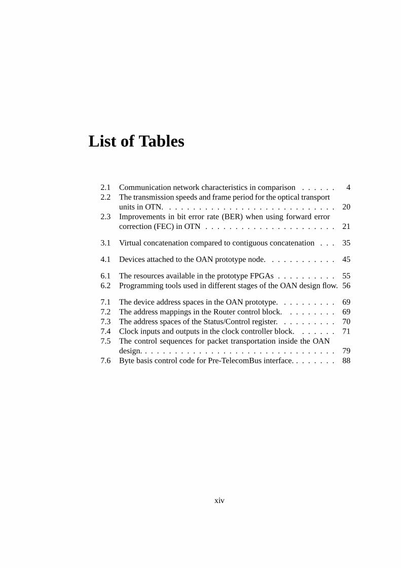
List of Tables
2.1 Communication network characteristics in comparison . . . . . . 42.2 The transmission speeds and frame period for the optical transport
units in OTN. . . . . . . . . . . . . . . . . . . . . . . . . . . . . 202.3 Improvements in bit error rate (BER) when using forward error
correction (FEC) in OTN . . . . . . . . . . . . . . . . . . . . . . 21
3.1 Virtual concatenation compared to contiguous concatenation . . . 35
4.1 Devices attached to the OAN prototype node. . . . . . . . . . . . 45
6.1 The resources available in the prototype FPGAs . . . . . . . . . . 556.2 Programming tools used in different stages of the OAN design flow. 56
7.1 The device address spaces in the OAN prototype. . . . . . . . . . 697.2 The address mappings in the Router control block. . . . . . . . . 697.3 The address spaces of the Status/Control register. . . . . . . . . . 707.4 Clock inputs and outputs in the clock controller block. . . . . . . 717.5 The control sequences for packet transportation inside the OAN
design. . . . . . . . . . . . . . . . . . . . . . . . . . . . . . . . . 797.6 Byte basis control code for Pre-TelecomBus interface. . . . . . . . 88
xiv
Chapter 1
Introduction
The continuing development of computing and memory management capabilitiesof computers has brought out new challenges to networking technologies. Thebandwidth is no longer a problem, but today it is the network management andmore importantly the availability of new type of services, real-time and streamingmedia. The increase in bandwidth together with developments in end-user equip-ment, especially in wireless one, has encouraged researchers to find new ways toutilise this emerging possibility in communications. However, the quality of con-nection in two-way communication is sensitive for the end-to-end transmissiondelay. Today, most of the datacom networks suffer from long delays and espe-cially from high packet delay variation, which makes the current situation evenworse.
Enabled by the technologies already developed, the transfer speed in a point-to-point connection can be almost as high as we like. Point-to-point connectionsare used as building blocks of larger networks and the sufficient connection band-width is determined within the network. The available capacity of point-to-pointconnection can be most efficiently utilised in Wide Area Networks (WANs) andLocal Area Networks (LANs), where the traffic is processed transparently leavingthe technology specific processing for Metropolitan Area Networks (MANs) tohandle. Most of the used telecommunication technologies come across in MAN,where a variety of conversions are needed between them. These conversions areslow and complex and have slowed down the development of metropolitan areanetworking, while other areas of networking have experienced major improve-ments. This is why the present MAN can be seen as a bottleneck for the transferspeed of the whole network [Inc02c].
1
1.1. MOTIVATION
1.1 Motivation
The National technology agency (TEKES)-funded project called Optical AccessNetworking (OAN)1 is a three-year project with several participants. The goal ofthe project is to implement a test network for development of new metropolitanarea services and network structures. In this project, most of the test networkfunctionality will be implemented with programmable logic. Programmable logicdevices can be programmed over and over again, which gives much flexibility tothe design, because different variations of the programs can be easily tested. Inaddition, they are large of their size and provide efficient processing abilities forthe design. Of course, this is only when these Field Programmable Gate Arrays(FPGAs) are programmed properly, which is my task in this project and moredeeply discussed later in this thesis.
1.2 Goal
The goal of this thesis is to identify what kind of requirements the future opticalaccess network gives for the underlying transport network, find ways to supportthese requirements, evaluate them and provide a Hardware Description Language(HDL) design for the FPGAs in the OAN network prototype.
1.3 Structure
After this brief introduction the rest of the thesis will be structured as follows.Chapter 2 introduces the reader to the characteristics of networks today, cover-ing some of the networking history together with key technologies and methods.Chapter 3 carries on the issue and reveals the nature of the future communicationnetworks. After that, in chapter 4 the research project called OAN is presented.Chapter 5 discusses the methodology of HDL-implementation. The options forthe OAN HDL design are presented in chapter 6 and the final design in chapter 7.Finally, the conclusions of the thesis are presented in chapter 8.
1Discussed more deeply in chapter 4
2
Chapter 2
Communication networks today
The first remarkable development in long distance communication was the in-vention of optical telegraph in 1791 [Bel03]. Since then, the desire for topicalinformation among people has been fulfilled with the help of inventions like elec-trical telegraph, telephone, radio and television. In all of these communicationmethods, the information from sender to receiver is transported over a certaintransmission media, usually air or cable and today even optical fibre. The needfor transmission media has lead to a development of communication networks,which have now evolved to a situation where three separated networks can beidentified: telephony, data communications and broadcast networks [Arm97].
The overlaid structure of the communication networks today is depicted in figure2.1. From the figure we can see that broadcast networks comprise of separatedlocal and regional networks, which are designed for high downstream bandwidthand limited upstream bandwidth, providing communication from one to many.Because of the nature of the traffic, the bandwidth in datacom and telecom net-works is usually the same in both directions. Differently from broadcast networks,telecom and datacom networks have some common parts in their structures. Atleast the core network is built in a way that both traffics could be transmitted overthe same routes, not necessarily over the same physical network. From these net-works, the telecom network was the first one to be built and eventually it reachedalmost every apartment worldwide1. Furthermore, the datacom networks existmainly inside corporations as separated islands, which are then interconnectedforming the Internet. The telecom network is mostly used for voice, but more of-ten it is the end-users’ only way to access datacom networks. For this reason, thecommon parts in telecom and datacom transport networks are the interconnections
1At least this was the case in industrial countries.
3
2.1. ACCESS NETWORK
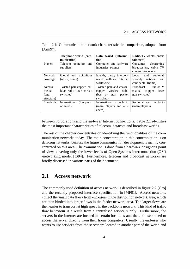
Table 2.1: Communication network characteristics in comparison, adopted from[Arm97].
Telephone world (com-munication)
Data world (informa-tion)
Radio/TV world (enter-tainment)
Players Telecom operators andsuppliers
Computer and softwareindustries, science
Consumer electronics,broadcasters, cable TV,content producers
Networkcoverage
Global and ubiquitous(office, home)
Islands, partly intercon-nected (office), Internetworldwide
Local and regional,scarcely national andcontinental (home)
Accessmedia(andstructure)
Twisted-pair copper, cel-lular radio (star, circuitswitched)
Twisted-pair and coaxialcopper, wireless radio(bus or star, packetswitched)
Broadcast radio/TV,coaxial copper (tree,non-switched)
Standards International (long-termoriented)
International or de facto(main players and alli-ances)
Regional and de facto(main players)
between corporations and the end-user Internet connections. Table 2.1 identifiesthe most important characteristics of telecom, datacom and broadcast worlds.
The rest of the chapter concentrates on identifying the functionalities of the com-munication networks today. The main concentration in this contemplation is ondatacom networks, because the future communication development is mainly con-centrated on this area. The examination is done from a hardware designer’s pointof view, covering only the lower levels of Open Systems Interconnection (OSI)-networking model [fS94]. Furthermore, telecom and broadcast networks arebriefly discussed in various parts of the document.
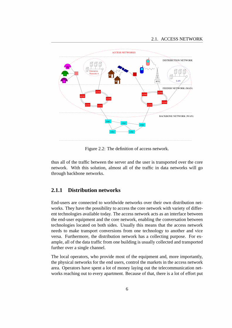
2.1 Access network
The commonly used definition of access network is described in figure 2.2 [Gro]and the recently proposed interface specification in [MF01]. Access networkscollect the small data flows from end-users in the distribution network area, whichare then binded into larger flows in the feeder network area. The larger flows arethen easier to transport at high speed in the backbone network. This kind of trafficflow behaviour is a result from a centralised service supply. Furthermore, theservers in the Internet are located in certain locations and the end-users need toaccess the server directly from their home computers. Usually, the end-user whowants to use services from the server are located in another part of the world and
4

2.1. ACCESS NETWORK
xDSL
RADIO
TV
TV
SAN
TRANSPORT NETWORKMAN MAN
MAN
WAN
TELECOM NETWORK
DATACOM NETWORK
BROADCAST NETWORKS
EnterpriseNetwork
BTS
BTS
LANSERVICE
OXC
OXCOXC
OXC
ADM ADMADMADM
ADM ADM
CATV
CATV
ADM
OXC
ADM
ADMADM
ADM
ADM ADM
Figure 2.1: The overlaid structure of communication networks.
5
2.1. ACCESS NETWORK
EnterpriseNetwork A
ACCESS NETWORKS
FEEDER NETWORK (MAN)
BACKBONE NETWORK (WAN)
DISTRIBUTION NETWORK
BTS LAN
OXC
ADM
OXC OXC
OXCOXC
ADM
ADM ADM
ADM
ADMADM
ADMADM
Figure 2.2: The definition of access network.
thus all of the traffic between the server and the user is transported over the corenetwork. With this solution, almost all of the traffic in data networks will gothrough backbone networks.
2.1.1 Distribution networks
End-users are connected to worldwide networks over their own distribution net-works. They have the possibility to access the core network with variety of differ-ent technologies available today. The access network acts as an interface betweenthe end-user equipment and the core network, enabling the conversation betweentechnologies located on both sides. Usually this means that the access networkneeds to make transport conversions from one technology to another and viceversa. Furthermore, the distribution network has a collecting purpose. For ex-ample, all of the data traffic from one building is usually collected and transportedfurther over a single channel.
The local operators, who provide most of the equipment and, more importantly,the physical networks for the end users, control the markets in the access networkarea. Operators have spent a lot of money laying out the telecommunication net-works reaching out to every apartment. Because of that, there is a lot of effort put
6
2.1. ACCESS NETWORK
PDH
xDSL / ISDN
BTS
COAXIALFIXED PAIR WIRELESS
Mobile
CATV
Satellite
Modem
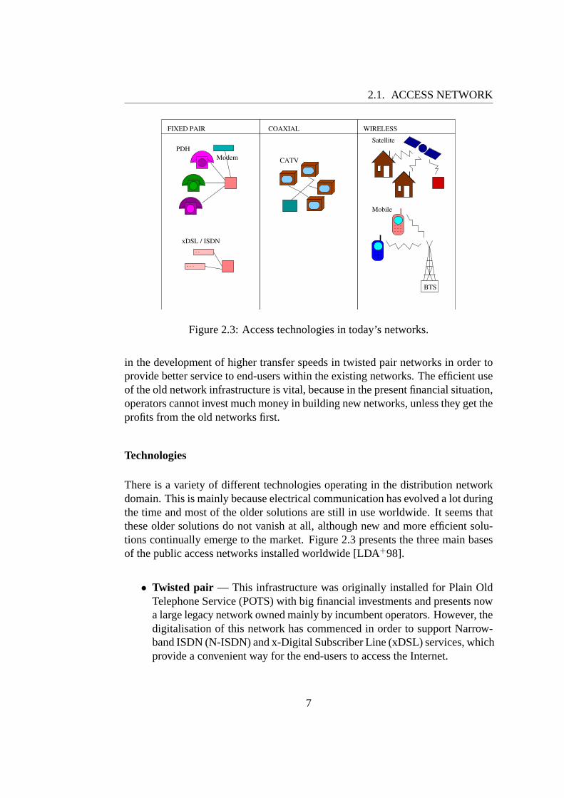
Figure 2.3: Access technologies in today’s networks.
in the development of higher transfer speeds in twisted pair networks in order toprovide better service to end-users within the existing networks. The efficient useof the old network infrastructure is vital, because in the present financial situation,operators cannot invest much money in building new networks, unless they get theprofits from the old networks first.
Technologies
There is a variety of different technologies operating in the distribution networkdomain. This is mainly because electrical communication has evolved a lot duringthe time and most of the older solutions are still in use worldwide. It seems thatthese older solutions do not vanish at all, although new and more efficient solu-tions continually emerge to the market. Figure 2.3 presents the three main basesof the public access networks installed worldwide [LDA+98].
• Twisted pair — This infrastructure was originally installed for Plain OldTelephone Service (POTS) with big financial investments and presents nowa large legacy network owned mainly by incumbent operators. However, thedigitalisation of this network has commenced in order to support Narrow-band ISDN (N-ISDN) and x-Digital Subscriber Line (xDSL) services, whichprovide a convenient way for the end-users to access the Internet.
7
2.1. ACCESS NETWORK
• Coaxial — These networks were originally installed for Cable AntennaTelevision (CATV), which are analogue in nature and characterised by treeand branch structure, enabling large downstream bandwidth but limited up-stream bandwidth.
• Wireless — The wireless transmission is quite new and rapidly growingfield in digital communications. The air interface has its own limits to datatransfer but the benefits seem to be worth the risk as the Global Systemfor Mobile communication (GSM) has already shown to us. On the otherhand, new ways to use the satellite transmission systems have emerged andtogether with the other systems, the phrase: “Future is wireless” does notseem so impossible after all.
Conversions between technologies are usually needed when small data flows areintegrated into larger ones or vice versa. For example, telecom networks use Ple-siochronic Digital Hierarchy (PDH) for that purpose. However, problems arisewhen improvements to transmission efficiency are needed and data flows fromdifferent technologies are attempted to converge into the same transmission pipe.This is mainly due to the issue that different technologies need different support-ing activities, which cannot be efficiently offered at the same time in the samemedia. For that reason several transmission paths between the same endpointsare needed to build and maintain, which is of course resource consumptive andexpensive.
This is mainly the situation between telecom and Storage Area Network (SAN)traffic or Internet and SAN traffic. For example, if a company has a phone centre,a separate data storage and an Internet connection, all of them need to be transpor-ted over separate fibres or cables. As an exception, the Synchronous Digital Hier-archy (SDH) and Synchronous Optical Network (SONET)2 technologies providea convenient way to transport Internet and telecom traffic simultaneously over thesame media. However, the data storage traffic cannot be transported with the helpof SDH. And because of the implementation costs of the SDH technology, it isnot suitable to be implemented outside MAN or WAN.
8

2.1. ACCESS NETWORK
BACKBONEMETRO
AGGREGATIONMETRO
ACCESSBROADBAND
ACCESSMETRO
xDSL
CO − Central OfficeAN − Access Node
DATA CENTER
SAN
SERVER
LAN
BTS
ANAN
AN
AN
AN
ANAN
AN
AN
CO
CO
Figure 2.4: MAN traffic characteristics today.
2.1.2 Feeder networks
A typical MAN in today communications networks acts like a feeder network.The MAN has both an abstract and a specific definition, which are both defined in[Net03] with the following phrase:
“Conceptually, the MAN is a set of networks that work together to provide accessand services in a metro region. Specifically, a MAN is a single, separate, identi-fiable “metro area network” that is owned and run by a single network operator,usually a service provider or carrier.”
MANs collect the traffic from access networks and then feed it to the backbonenetwork. The traffic in a MAN is typically transparent from access to access, fromcore to access or from access to core network. Herein the Access Nodes (ANs)are only responsible for separating the incoming and merging the outgoing trafficflows from and to the metro transport pipe. Sometimes, certain InterworkingFunctions (IWF) may be needed to convert different technologies between eachother. Furthermore, Central Offices (COs) act as connection points between otherMANs or backbone networks. This behaviour can be seen in figure 2.4, which alsopresents the different types of access traffic in MANs today [Inc02c] [Mol88]. Thedifferent types of traffic in MAN are more deeply discussed later.
2International Telecommunication Union, Telecommunication standardisation sector (ITU-T)has defined the SONET to be a subset of SDH, the acronym SDH is used in the rest of the thesisto refer both SDH and SONET.
9
2.1. ACCESS NETWORK
Services
In order to function properly MAN has to offer certain services for access net-work technologies. First of all, the network configuration needs to be flexible, sothat the changes in the network structure3 can be managed quickly and withoutdisturbing the traffic flow. At the same time the available bandwidth is allocatedbetween different traffic flows in a way that data will not overflow in buffers andthe utilisation of the bandwidth is as high as possible. In addition, several otherservices are provided depending on the MAN traffic type, presented in figure 2.4,and the following will list few of them [CSK88] [MHPG91].
• Metro access— This category includes variety of technologies, rangingfrom newly developed wireless technologies to older ones, which were usedalready in the early days of communication networks. From MAN, thesetechnologies require the following services: LAN interconnection, supportfor voice, connection-oriented or connectionless services, switched or non-switched networking between hosts, broadcast and multicast traffic.
• Broadband access— This category includes more recent technologies,specialised in one or two way broadband transmission. The broadbandtransmission technologies over cable (CATV) or fixed pair (xDSL) are olderthan these newly developed wireless technologies, now emerging to mar-ket. Technologies in this category need multimedia, security and mobilityenabling services from MAN.
• Metro aggregation — This category includes all the traffic between dif-ferent MANs. This traffic is usually transported over a single pipe, wherebandwidth allocation together with traffic monitoring services is required.This stands for both, incoming and outgoing traffic.
• Data centre — Technologies in this category are specialised in data pro-cessing and data storage. Corporations use data centres and for that reasonthey require secure and fast connections from and to MAN. In today’s net-works, connections to data centres use separated fibres, providing low delaysand high bandwidths. The server traffic is more one way, from servers toend-users and is not so sensitive for delays.
• Metro backbone— This is the interface from MAN to backbone network.The traffic type here is similar to the connecting traffic between MANs, butit usually requires more bandwidth. For that reason the technologies used
3Adding and removing of nodes, fibre cuts or other errors.
10
2.2. TRANSPORT NETWORKS
EnterpriseNetwork A
BACKBONE NETWORK (WAN)
FEEDER NETWORK (MAN)
TRANSPORT NETWORKS
DISTRIBUTION NETWORK
BTS LAN
OXC
ADM
OXC OXC
OXCOXC
ADM
ADM ADM
ADM
ADMADM
ADMADM
Figure 2.5: The definition of transport network.
here may differ from the technologies used connecting MANs. Depend-ing on the technology (SDH, Asynchronous Transfer Mode (ATM), PacketOver SDH (POS), Dense Wavelength Division Multiplexing (DWDM)),bandwidth allocation and other higher layer management task are neededto support.
One important concept in data networks is the Quality of Service (QoS), whichhas attracted lots of discussion and is coming more important every day. It isa concept by which applications may indicate and even negotiate their specificservice requirements to the network. Furthermore, the purpose is to define ways toguarantee certain delay and bandwidth limits for networking equipment [GJS03].The need for QoS in networking emerges from the fact that the default servicein many packet networks has been the best-effort service, where all applicationsget the same service. Now the amount of data traffic has increased and it is usedin new ways. At the moment, the lack of strict delay and bandwidth guaranteesprevents the connectionless transport to emerge into new areas.
11

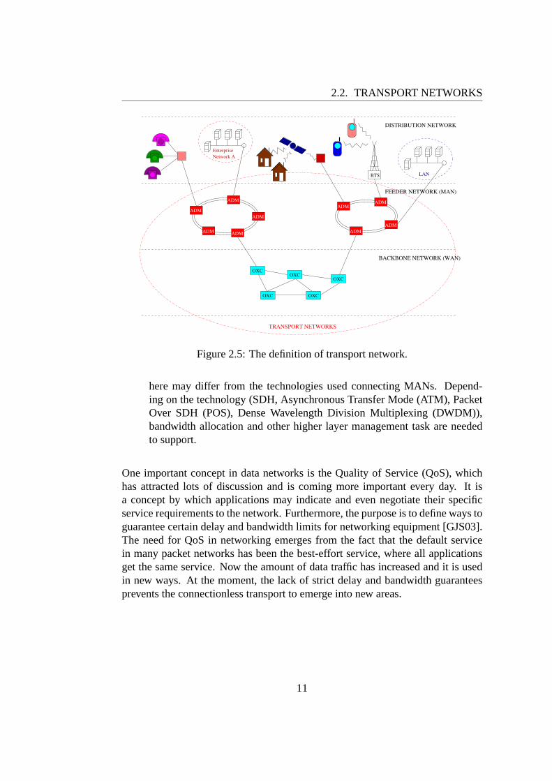
2.2. TRANSPORT NETWORKS
2.2 Transport networks
The traffic characteristics in MAN and WAN differ from each other in transferspeed, connection distances and in service models. Still the transport networkcovers both of these areas, as depicted in figure 2.5. This is because the nature oftransport networks is to provide fast data transfer activities, needed in both MANand WAN. Furthermore, the transport network does not include services otherthan formed from the need to transfer data efficiently and error free from point-to-point. For this reason, the access network services provided by MAN are part ofthe feeder network functionalities, splitting the functionalities of MAN betweentransport and feeder networks.
Transport networks today are mainly optical and their bandwidths depend on thenumber of light paths included in the system. Adding more light paths into thenetwork, the bandwidth can be increased enormously and the only limit seems tobe the price of the equipment. However, these kinds of systems have just emergedto the markets and used mainly in the core network area. Furthermore, the mostimportant transport networks, optical networks are more deeply discussed in sec-tion 2.4. In addition, high-bandwidth satellite connections can be used to transportdata traffic as well.
2.2.1 Data centric services
In order to transport traffic efficiently, certain transporting functionalities are neededfrom the underlying network. As transport networks are composed of point-to-point links, the transporting functionalities they provide are mainly concentratedon monitoring the link state and the traffic flow. Herein the transported data flowis transferred as it is, without deeper processing of its content. Transport net-works have their own management functions for network configuration, routingand maintenance. These tasks are responsible for forwarding data packets anddirecting dataflow towards the receiver. The following list will identify the mainfunctionalities provided by data transporting networks.
• Configuration, routing and maintenance— These activities are respons-ible for building and updating of routing tables when the network is con-figured at the first time or when the structure of the network changes. Thechange in network structure can happen because of a fibre cut or when oldnodes are removed or new ones added in the network. After these functionsare performed properly, the forwarding of packets will be automatic.
12

2.2. TRANSPORT NETWORKS
• Packet forwarding — This operation is responsible for the forwarding ofdata packets. In other words, the incoming data packet is transmitted outfrom a specific port of the routing device. The routing table according tothe address of the packet defines the output port.
• Bandwidth allocation — This activity is responsible for sharing the avail-able bandwidth between connections or data flows. Higher priority flowswill have stable connections and lower priority traffic is transported if thereis still bandwidth left in the transportation pipe.
• Link monitoring — This functionality is responsible for the monitoring ofthe state of the transportation link between certain end-points. The manage-ment application is informed, whenever the link changes it state. The linkcan have different states or alarms, depending on the used technology.
• Traffic balance — This is an important activity when the full bandwidth ofthe transportation pipe needs to be utilised. Packet oriented traffic is burstyand it is possible that the channel transportation pipe is not wholly utilisedall of the time, or the traffic in the channel exceeds the limit reserved for thechannel. To keep the pipe full all of the time, the traffic needs to be balancedin an appropriate way.
• Error monitoring — usually the transport network tracks the Bit ErrorRate (BER) of the transmission path or at least identifies the erred trans-mission blocks. In some cases, mainly in wireless transfer, the transmissionerrors can be corrected to a certain point in the receiver side.
2.2.2 Synchronisation
In the past, nodes in the network were connected asynchronously in a way thatevery node had their own clocks and the traffic in the network was received andtransmitted with this clock. This resulted problems, because electricity4 propag-ates at a certain speed. Depending on the distance from node to node, the syn-chronisation of the received data stream according to the receiver clock could beexact, totally out of synchronisation or something in between. If the network is outof synchronisation, it is very probable that the data cannot be read correctly andfor this reason, synchronised networks were developed. The synchronisation res-ulted in better functioning networks and the transfer speed was increased rapidlytogether with the decrease in network delay. In synchronised networks, the nodes
4At that time, networks were all electrical.
13
2.3. NETWORK TOPOLOGIES
POINT−TO−POINT STAR TREE RING MESH
Figure 2.6: Topologies used in networks today.
synchronise their clocks according to incoming data. In the past, networks usedgeneral clock distribution as their synchronisation method, but today the DelayLocked Loop (DLL) and Phase Locked Loop (PLL) -methods are more widelyused in transport networks world-wide. Together with clock synchronisation thenetworks need a common frame and network synchronisation methods as well,but these are specified separately within the technology limits [Bre02].
2.3 Network topologies
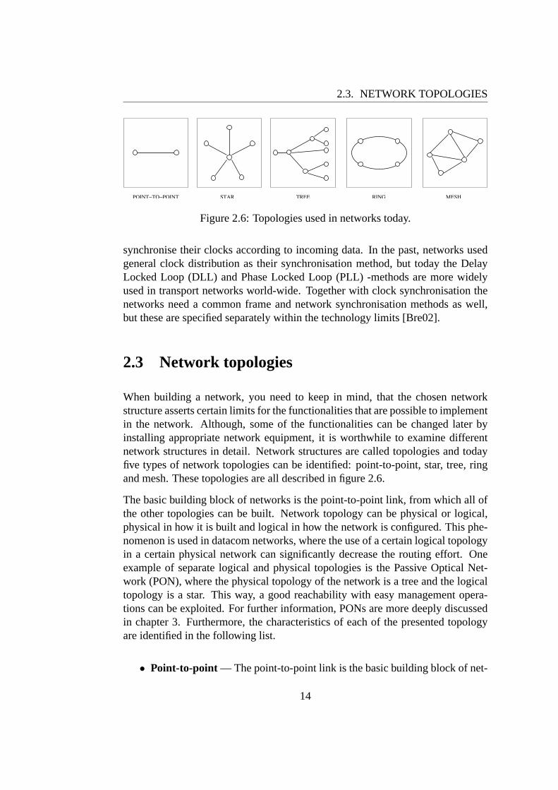
When building a network, you need to keep in mind, that the chosen networkstructure asserts certain limits for the functionalities that are possible to implementin the network. Although, some of the functionalities can be changed later byinstalling appropriate network equipment, it is worthwhile to examine differentnetwork structures in detail. Network structures are called topologies and todayfive types of network topologies can be identified: point-to-point, star, tree, ringand mesh. These topologies are all described in figure 2.6.
The basic building block of networks is the point-to-point link, from which all ofthe other topologies can be built. Network topology can be physical or logical,physical in how it is built and logical in how the network is configured. This phe-nomenon is used in datacom networks, where the use of a certain logical topologyin a certain physical network can significantly decrease the routing effort. Oneexample of separate logical and physical topologies is the Passive Optical Net-work (PON), where the physical topology of the network is a tree and the logicaltopology is a star. This way, a good reachability with easy management opera-tions can be exploited. For further information, PONs are more deeply discussedin chapter 3. Furthermore, the characteristics of each of the presented topologyare identified in the following list.
• Point-to-point — The point-to-point link is the basic building block of net-
14
2.4. OPTICAL NETWORKS
works, where the lower level management and monitoring of network con-centrates. The management of a point-to-point connection as such is easyand requires little management traffic. However, this is not the case whenseveral point-to-point connections form a large network, because now thewhole network is to be managed.
• Star — In the star network, every node can reach all of the other nodesthrough the central node. This results in good accessibility between nodes,but the downsize of this feature is that the central node needs to be capableof handling all of the traffic in the network. This topology is popular insmaller networks, because it is easy to build and maintain.
• Tree — The tree structure is widely used in terrestrial broadcast networks,like the CATV, because with this topology all of the end-users can be reachedby simply forwarding the transmission down to the network. This results ina low cost and reliable network, because the forwarding equipment is simpleand cheap. When this topology is used for two-way traffic, the upstreambandwidth is shared between all the users and often it is quite limited. Onthe other hand, the downstream bandwidth can be high, depending on theusage of the network.
• Ring — The ring topology is the most popular one in the metropolitan area,because it provides good survivability features and spreads over a large areaproviding good base for the access networks.
• Mesh— Nodes in the mesh topology have great amount of routes from oneplace to another and this results in a very complex network structure, espe-cially when the amount of nodes is high in the network. In this structure,protection and accessibility levels can be high when appropriate routingmethods are used. However, finding or developing these methods is a verydemanding task and usually results in complex solutions.
2.4 Optical Networks
From the early 1980’s, the telecommunication networks have evolved from asyn-chronous to synchronous and then optical, still trying to reach for all-optical tech-niques. SDH was the first functional optical network in the telecom driven in-dustry. Now after two decades from its development this network is responsiblefor most of the transferred telecommunication traffic worldwide. However, it does
15
2.4. OPTICAL NETWORKS
not support the transfer speeds typical to the core networks, and other technolo-gies are needed for the purpose. Recently developed optical signal amplificationand Wavelength Division Multiplexing (WDM) have revolutionised long-distancetransport, resulting in capacity expansion, cost reduction and operations simpli-fication in core networking [ASFG+98].
WDM is a technique where several light paths can be transported simultaneouslyin one fibre. This technique is already widely tested and implemented in the mostimportant parts of the core networks. It seems that, in the future, this techniquewill be widely implemented in the other parts of the network as well. However,the complexity of the network management operations increases as the numberof light paths in the network increases. This means that the cost of managementis high, when there are a great number of light paths implemented in the WDMnetwork. For this reason, the WDM is usually used to increase the capacity of thebottleneck links only. To ease the management operations in the WDM network,the concept called Optical Transport Network (OTN) has been developed. OTNsare WDM networks that have both, traffic and light path management systemsimplemented. There is a lot of flexibility how these OTNs can be deployed, de-pending on the transport services to be provided [Cav00]. Furthermore, the nextthree sections will give a more detailed presentation about the SDH, the WDMand the OTN technologies.
2.4.1 Synchronous Digital Hierarchy (SDH)
SDH was originally designed to replace PDH based networks in transmission ofconnection-oriented telecom traffic in the beginning of 1980’s. At that time theconnectionless packet traffic was not common and nobody expected that this situ-ation would change much in the future. During the following years, SDH net-works were widely implemented all over the world and SDH is now the mostpopular network technology used today. However, the nature of the data traffichas changed since the early days, and the optimisation of SDH networks to bettersupport the connectionless data transfer has been a major issue during past fewyears. The reason for this development is the goal to provide better QoS for theemerging multimedia and real-time services.
The functionality in SDH is based on synchronised and standard sized frames,where the data packet or data stream can be inserted in any part of the frame,pointing its start with a specific pointer [Tek01]. This structure allows efficientmonitoring and management functionalities to be implemented and transportedinside SDH-headers. Furthermore, these headers give only three percent of extra
16
2.4. OPTICAL NETWORKS
overhead to the transport. The pointer-processed insertion of data packets or datastreams allows the frames to be filled wholly and no empty space is left betweenpackets in the frame. In addition, SDH has its own hierarchical system of howdifferent transmission technologies are inserted, first into containers and then intothe SDH-frame [Gor00]. SDH supports electrical and optical transport, but themanagement of the network is done electrically.
From the network owner, the operators, point of view the optimisation of the oldnetworks to better support the new requirements has been a major goal for theirdevelopment tasks. Their purpose is to save expenses by exploiting old networkinfrastructure as much as it is possible. At the moment, it seems that this stands forthe survival of SDH networks in the future. There are some advantages in the SDHtechnology already. It provides very efficient transport services and is the onlyone available today to transmit connection-oriented telecom traffic in its delaylimits, allowing simultaneous connectionless transport. The hierarchical framestructure of SDH enables bandwidth allocation and management between severalusers, although the legacy contiguous allocation is not so efficient in allocationgranularity [OSG02].
Packet over SDH (POS)
Clearly the development of networking has shown that the Internet Protocol (IP)packets would be the most popular form in transporting data in the networks. Fewyears ago somebody suggested that the most efficient way would be to transmitIP packets directly over fibre, without the complex OSI layer structure. After thisthe whole industry was talking about “IP-over light” and other synonyms for that.The more optimistic ones actually believed that this hype could be the truth aftera few years of research [MBK01]. However, the research efforts made for thegoal showed that it was not possible to have efficient transport of traffic withoutthe functionalities provided by these OSI layers [BRM01] and the matter was soonforgotten. However, the discussion brought more attention to the already availableIP over fibre techniques, especially easy to use IP over SDH techniques. Theseare briefly presented in the following list.
• IP over SDH — This technique enables the direct transport of IP-packets(Point-to-Point Protocol (PPP) in High level Data Link Control (HDLC)frames) over SDH-link. The transported IP-packet is mapped into a con-tainer, which is then inserted into an SDH-frame. This operation does notinterfere with the other ongoing transporting actions, allowing other SDHtransport as well.
17

2.4. OPTICAL NETWORKS
• IP over ATM over SDH — This technique works similarly as the formerone. The difference here is that first the IP-packet is mapped into ATM-frames, which are then mapped into SDH frame. With this method, a lotof bandwidth is lost into overhead, caused by ATM-headers. As a result,reliability and other functionalities of the ATM can be integrated into SDH.Still, because of the overhead, the efficiency of this method is low.
• IP over Ethernet over SDH — In this technique ATM is replaced withEthernet. The use of Ethernet over SDH requires less overhead than the useof ATM over SDH. On the other hand, the services provided by the Ethernetare not as efficient as the ones, provided by ATM. However, Ethernet fulfilsthe requirements for normal transporting operations quite well.
2.4.2 Wavelength Division Multiplexing (WDM)
One of the research trends in today’s networking is the development of all-opticalnetwork components and structures. This is an area, where a lot of developmentis needed before the final equipment can enter the markets. Before all-opticaltechnologies, the WDM technology is the way to exploit the huge opto-electronicbandwidth mismatch in networking. WDM uses a technique called multiplexing,which is defined in [BP01] with a following phrase:
“Multiplexing is the simultaneous transmission of different messages over thecommunication network through a partitioning of the available bandwidth orother resource”.
There are two types of multiplexing used in optical communication, Time Divi-sion Multiplexing (TDM) and Frequency Division Multiplexing (FDM), wherethe FDM is the method used in WDM. With the help of TDM, slower flows canbe multiplexed consecutively into one light path, which is then easier to transportat higher speed. After TDM, WDM is used to multiplex the different light pathsinto the same fibre [Muk97].
By this way, multiple end-users may all have their own channels through a singlefibre and the bandwidth of the network can be increased easily. Today the WDMtechnique is already widely used in core networks, and it is emerging into theMAN area as well. With the help of WDM the available bandwidth now exceedsthe limit of 1 Tbps. The price of the WDM system is composed mainly of thenumber of optical channels needed, because every light path needs its own elec-trical and optical equipment and their management is complex [Muk97]. For thisreason, the cost of the equipment exceeding the transfer speed of 1 Tbps is high.
18

2.4. OPTICAL NETWORKS
ADM
SDHADM
SDH
ADMSDH
ADMSDH
ADMSDH
ADMSDH
ADMSDH
ADMSDH
ADM
ADMSDH
ADMSDH
ADMSDH
ADMSDH
ADMSDH
ADMSDH
ADMSDH
UNGROOMEDSDHADM
SDHADM
SDH
WADM
WADM
WADMWADM GROOMED
Figure 2.7: Traffic grooming in WDM networks.
Traffic Grooming
At the moment, it seems that WDM systems will be more widely utilised in net-working in the future. This means that the number of light paths in the networks isgoing to increase, which increases the network complexity as well. The increasedcomplexity brings new concerns into routing and network configuration tasks, andnew solutions are needed in that area. In addition, every light path needs it ownconversion equipment to convert the data from optical to electrical and vice versa.This equipment is relatively expensive, and it is good to try to decrease the num-ber needed. Usually, there is no need to have a connection between each of thenodes in the network. The complexity of the network could be decreased for ex-ample by providing certain light paths between certain nodes, leaving some lightpaths unconnected. By this way the network could be divided into different logicaltopologies, independently from the physical topology. This manipulation of net-work light paths is called grooming and it is defined in [BP01] with the followingphrase:
“Grooming is an industry term used to describe the optimisation of capacityutilisation in transport systems by means of cross-connections or conversionsbetween different transport systems or layers within the same system”.
With the help of grooming, the network could be optimised according to capa-city utilisation or the number of Add Drop Multiplexers (ADMs) needed in thenetwork. As an example, most of the traffic in ring network travels through con-secutive nodes, which are only responsible for the retransmission of the traffic.The ungroomed situation of an example ring network is presented in the left sideof figure 2.7. After grooming, few of the ADMs can be removed and the complex-
19

2.4. OPTICAL NETWORKS
Table 2.2: The transmission speeds and frame period for the optical transport unitsin OTN.
Optical channel Transport Unit Line Rate/Mbps Frame Period/ms
OTU1 2666 48,971OTU2 10709 12,191OTU3 43018 3,035
ity of the network is decreased. This groomed situation is presented in the rightside of figure 2.7. The extend of how much ADMs can be saved with groom-ing depends on the capacity needed between different nodes in the network. Thisneeds to be considered separately in every case. However, the optimisation taskbecomes quite complex when the size of the network increases. For that reason,new algorithms for the optimisation task are continually been developed [LGP01].In addition, grooming includes optimisation of multiple transport systems5 andmultiple layers of a single transportation system [BP01].
2.4.3 Optical Transport Network (OTN)
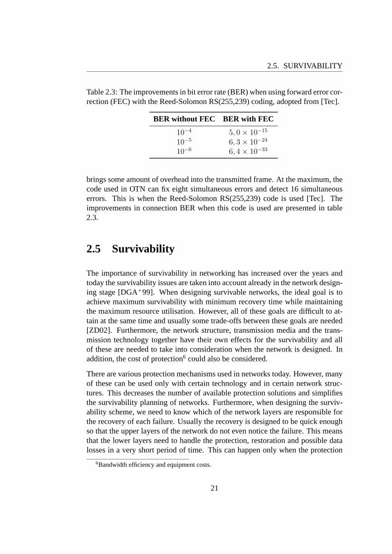
As discussed before, SDH cannot fully exploit the possibilities of the WDM tech-nology. To ease the management tasks in WDM networks, ITU-T study group15 has defined a new set of recommendations for optical transport networking[IT00b]. These include architectural, interfacing and management issues and fromnow on, I will apply to all them with the term Optical Transport Network (OTN).OTN has many similarities with SDH, like the hierarchical structure and frameformat. This makes sense, because the OTN is an improved version of SDH andregarded as a lifeline to increase the capacity in the future networking [Tec]. Cur-rently, there are three optical line rates defined for OTN, presented in table 2.2.The management of optical channels is the most important improvement in OTN.Furthermore, it has another new feature implemented in it, the Forward Error Cor-rection (FEC).
When the line rate of a certain optical channel is increased, the BER of that chan-nel will most probably increase too. This is because of the dispersion effect infibres, caused by their physical characteristics. If the BER of the connection in-creases, more efficient error correction mechanisms will be needed to provide thesame reliability as before. FEC is just the method for the purpose, although it
5Where the technology can be electrical, optical or microwave.
20
2.5. SURVIVABILITY
Table 2.3: The improvements in bit error rate (BER) when using forward error cor-rection (FEC) with the Reed-Solomon RS(255,239) coding, adopted from [Tec].
BER without FEC BER with FEC
10−4 5, 0× 10−15
10−5 6, 3× 10⁻²⁴
10−6 6, 4× 10⁻³³
brings some amount of overhead into the transmitted frame. At the maximum, thecode used in OTN can fix eight simultaneous errors and detect 16 simultaneouserrors. This is when the Reed-Solomon RS(255,239) code is used [Tec]. Theimprovements in connection BER when this code is used are presented in table2.3.
2.5 Survivability
The importance of survivability in networking has increased over the years andtoday the survivability issues are taken into account already in the network design-ing stage [DGA+99]. When designing survivable networks, the ideal goal is toachieve maximum survivability with minimum recovery time while maintainingthe maximum resource utilisation. However, all of these goals are difficult to at-tain at the same time and usually some trade-offs between these goals are needed[ZD02]. Furthermore, the network structure, transmission media and the trans-mission technology together have their own effects for the survivability and allof these are needed to take into consideration when the network is designed. Inaddition, the cost of protection6 could also be considered.
There are various protection mechanisms used in networks today. However, manyof these can be used only with certain technology and in certain network struc-tures. This decreases the number of available protection solutions and simplifiesthe survivability planning of networks. Furthermore, when designing the surviv-ability scheme, we need to know which of the network layers are responsible forthe recovery of each failure. Usually the recovery is designed to be quick enoughso that the upper layers of the network do not even notice the failure. This meansthat the lower layers need to handle the protection, restoration and possible datalosses in a very short period of time. This can happen only when the protection
6Bandwidth efficiency and equipment costs.
21
2.5. SURVIVABILITY
scheme is fully planned in advance [DGA+99].
Protection is the primary mechanism used to deal the failure. After the protec-tion function is completed, restoration is used to provide new routes or additionalresilience against further failures before the first failure is fixed [GR00]. Pro-tection mechanisms can be divided into electrical and optical protection, whichboth can be divided into link or path protection mechanisms. At the moment, thecommunication development is concentrated on optical communication and forthat reason, the optical protection methods have experienced great improvements.Furthermore, the optical protection mechanisms can be faster than the electricalprotection mechanisms, but more important is that some optical methods can beused passively, requiring cheaper and less complex devices. This is why the op-tical protection is coming more popular in networking.
22

Chapter 3
Communication networks tomorrow
In the future the networks are heading towards flexibility and scalability enablingnew ways for interoperability. The reason for this development can be derivedfrom the overlaid network model, presented in figure 2.1, and from the emergingnew services, which require more speed and new supporting functions from theunderlying networks. This means that the traffic in communication networks isonce again changing its characteristics. Previously, the change was from connection-oriented to connectionless transportation, but now a third type of traffic is emer-ging, called the real-time traffic [And02]. The real-time traffic has some of thefeatures from both of the connectionless and connection-oriented traffic, but stillthe current network structure prevents the efficient transport of this traffic. Fur-thermore, all of these three network types need to co-exist in the networks. Thistogether with the issues discussed in chapter 2 is pushing the development of com-munication networks towards convergence. The main target of discussion in thischapter is the characteristics of converge networks.
The problem in today’s networks lies in the metropolitan areas, where the com-plexity of access networks is a real problem. The great number of different ac-cessing technologies has been the reason for slow development in metropolitanarea networking for a long time. This is a real problem, because the legacy net-work structure cannot provide adequate support for the real-time traffic. It seemsthat the present MAN structure is not going to survive anymore. In the future,MANs need to be more adaptive and more intelligent and this means modifica-tions and developments to the current networks. For this reason, it is quite clearthat the metropolitan and access network areas are going to be a target for majordevelopments and improvements in the near future [LDA+98].
The speed of electrical signal processing in today’s transport networks is mov-
23
3.1. FUTURE CHARACTERISTICS
ing closer to the physical limit of silicon. At the moment, it seems ineluctablethat the limit will be reached some day and more advanced systems are neededto develop. The hope for finding faster data transportation methods has increasedefforts in the development of all-optical communication solutions, which are con-sidered to be the most technically superior in the long term [LDA+98][YYMD01].The problem in electrical networking is not the bandwidth, but rather the speedof how many packets can be forwarded in a certain time. However, in all-opticalnetworking the forwarding of packets could be faster, because there is no need foropto-electrical and electro-optical conversions. With WDM we can already easilyincrease the network link bandwidth to meet our requirements, but the manage-ment of large WDM networks is a much harder task and the equipment is moreexpensive. The cost of the equipment is much lower with optical equipment, es-pecially when passive optical network elements are used. Furthermore, the com-plexity of the management operations may be decreased with optical networking.
3.1 Future characteristics
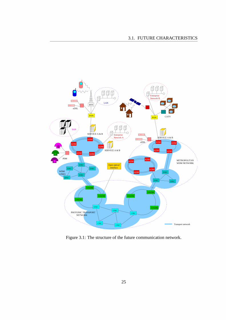
This section will discuss future network requirements and the realisation strategiesconcerning future networking in access, metropolitan and core network areas. Theareas of research in telecommunications are briefly described together with the re-quirements and possible solutions for the future networking. The main goal is tofind the characteristics of the future data traffic and service functionalities. Butfirst, the most probable structure of the future communication network is illus-trated in figure 3.1 [LDA+98][SS99][YJH+00][STS02][Con89] and more deeplydiscussed later in this section.
Today, the end-user behaviour has greater effect on the network requirementsthan it has had before. The wireless communication techniques and end-userequipment are developing rapidly, attracting more and more people to buy theequipment and start using the available wireless services. In addition, the amountof data traffic in communications networks will increase continuously, bringingscalability and multiservice requirements to the existing networks. Furthermore,the operators are tired of maintaining overlapping network structures and are readyto invest on converged network solutions to save money from the management op-erations and concurrently provide better service for end-users. Even more moneycould be saved with automatic fault tolerant networks, which could use automaticprotection and restoration mechanisms for fast recovery after network failure. Inaddition, automatic switching and network management issues are coming moreimportant also [HM02]. Yet, the end-users and enterprises are more and more
24
3.1. FUTURE CHARACTERISTICS
Transport network
PDH
xDSL
xDSL
LAN
EnterpriseNetwork B
SAN
EnterpriseNetwork A
SERVICE A & B
SERVICE A & B
SERVICE A & B
BTS
OADM
OADM
OADM
OADM
OADM
OADM
OXC
OXC
OXC
OXC
OXC
ADM
ADM ADM
ADM
ADM
ADMADM
ADMADM
ADM
ADM ADM
ADM
Open opticalinterface
PON CATVPON
PHOTONIC TRANSPORTNETWORK
METROPOLITANWDM NETWORK
WDMLINKS DXC
DXC
DXC
DXC
DXCDXC DXC
DXC
Figure 3.1: The structure of the future communication network.
25

3.1. FUTURE CHARACTERISTICS
concerned about the network security and information copyrights. These have de-veloped into a major issue, due to Internet banking and shopping. All this haslead to a desire to develop a new kind of network, where traffic flow between end-points would happen transparently in a way that the underlying network does notsee or process the transported data at all.
Transparent transfer is one of the most often mentioned solutions for the problemsin today’s networking. This is because the network needs to support differentkinds of services with different requirements. So far, providing separate networksfor different tasks or technologies has been enough. With the help of transparenttransfer, different networks could be integrated into single network architecture.In legacy networks, the transmitted data needs to be processed with required wayin every network node and to provide the support for all of the available tech-nologies has been out of the question. The transparent transfer provides a way totransport the traffic through the network without technology dependent processingtasks. This is done by encapsulating the data into certain technology, capable ofhandling the transportation tasks. ATM is one of the technologies providing trans-parent transfer. The reason why ATM is not used here is the already laid SDH net-work structures, which are not capable for efficient ATM-transport. On the otherhand, the protection and survivability issues in ATM are not in the same level asin the SDH and the amount of overhead in ATM exceeds the amount of overheadin other networks. At least this is the truth so far. Anyway, the opinions on usingATM or other system as a new transport network vary considerably [Sep02].
3.1.1 Distribution networks
It seems that the number of access technologies is not going to decrease in thefuture but the opposite. This means that a greater number of conversions betweentechnologies will be needed in the future. Supporting all of the needed interwork-ing functions in the future in access region will result in complexity expansionand problems. This is not desirable, and one way to avoid this is to move theinterworking functions towards distribution networks. This means that the trans-parent transfer will reach the access region as well. Together with this, the amountof bandwidth in access networks is going to increase in the near future when themultimedia services will come into the reach of people. The trend can already beseen as an increase of cable and xDSL connections on the end-user markets. Atthe moment, the most promising solution to solve the bandwidth increase and theinterworking problems seems to be the PON, which allows transparent optical datatransfer over MANs with low cost passive optical equipment [Com01]. The ideabehind this solution is the passive optical feeder network, which collects the data
26
3.1. FUTURE CHARACTERISTICS
from the access domain and feeds it to the transport network for the transmission.The PON technology is more deeply discussed in section 3.2.1.
New wireless transmission techniques emerge to the market continuously. Thereare multiple developed and yet undiscovered ways to use these new technologies,which is why they are recognised as a part of the future access technologies. In thefuture, mobile equipment will come more intelligent and the need for bandwidthincreases. However, it seems that high-speed transmissions cannot be suppor-ted over long distances and the user needs to accept the speed he or she gets.The wireless networking is said to move into a direction where mobile equipmentcan select the best technology for its purposes from all of the available wirelesstechnologies [Tec02]. This switching between technologies does bring new con-siderations to wireless security. In addition, operators are searching new ways toexploit the existing CATV networks in data transfer as well.
3.1.2 Metropolitan area networks
As discussed before, the metropolitan area networking has been one of the mainareas of research. This is because the legacy networks cannot fully support thenew transportation requirements. The problem in MAN is the great number ofaccess technologies, which creates complexity. Because of the complex structure,the transport network cannot provide an adequate QoS support. The most popu-lar solution for these problems in the industry seems to be a flexible and scalableoptical hybrid network [HV02]. The hybrid network is a network, where one orseveral transport technologies are supported directly over some other transportsystem. For example, this is the case in different Packet Over SDH (POS) tech-nologies, where the other technology is supported over SDH. However, the POSsolution as such is not flexible and scalable enough, and a scheme called Data overSDH (DoS) is developed for the purpose.
With DoS, the traffic flow between end-points will happen transparently, enablingmore flexible transport with dynamic resource allocation and with the base forpresent and future services [GRF02]. It has a simple layered structure, which onthe other side interfaces with access network technologies and on one side withtransport network technologies. With this flexible interface, a variety of techno-logies could be transported simultaneously over a single transport network. Thissolution will decrease the amount of physical connections needed in networks,because now the telecom, SAN and datacom traffic can be transported simultan-eously over a single fibre [MYMN02]. The DoS scheme is more deeply discussedlater in the thesis.
27
3.1. FUTURE CHARACTERISTICS
Although the execution of interworking functions is moving towards distributionnetworks and end-user terminals, certain services still need to be supported inMAN level. One aggregate of these services is the network security, where theVirtual Private Network (VPN) seems to be the solution for enterprise networkingand the IP Security (IPsec) a promising new technique to be used elsewhere. Fur-thermore, intelligent servers have been developed for some time, and when theyare to be installed, services will move closer to end-users and there is no need toaccess them over the core network. This means that copies of the original servicewill be stored in the areas where the users of that service physically are. This willbe responsible for the moving of the traffic from WANs to MANs [Inc02c]. Fur-thermore the operation of intelligent servers may require other services as well.
3.1.3 Transport networks
Transport networks today can handle the current traffic quite well. However, itseems that new techniques are needed when the users of the Internet are begin-ning to use more bandwidth consuming services. Although, the WDM techniqueis the key for high bandwidth, the speed of electrical data processing in trans-port networks cannot be increased unlimitedly from what it is now. Furthermore,the opto-electrical conversions are expensive and resource consumptive to imple-ment, which is a major cost for network updates. For that reason, the research onthe transport network side has mainly concentrated on developing all-optical orphotonic networks, where the transmission would happen without electro-opticalconversions and the network switching could be done almost in real-time. Further-more, the WDM technology with all-optical packet switching is proposed to be thecore technology in metropolitan area as well [HM02][YYMD01]. The increase ofbandwidth is no longer the main goal in network development. The operatorshave calculated that one major cost factor for them is the network maintenance.Because of that, they would like to have all of their maintenance functions as auto-matic as possible in the future. This would mean more survivability features andease of management, preferably remotely controlled. Furthermore, the character-istic of traffic has changed and to respond for the different transportation needs,networks need to be more scalable and flexible than before. The main issue hereis the ability to allocate traffic into different pipes or channels, depending on theQoS requirements. Together with this, error monitoring, correction and protectionissues are coming more important [Par02].
28
3.2. FUTURE TECHNOLOGIES
3.1.4 Optical networks
There has been a lot of success in all-optical networking area, but the real break-through solution or technology is still waiting to be found. It seems that readinginformation directly from light without opto-electrical conversions is a hard taskand nobody so far has figured out how to do it. The research in this field continuesintensively, although nobody even knows if any solution is possible to be found atall. In conventional networks, the whole packet is needed to convert from opticalto electrical before re-transmitting. This is quite resource consuming, because theforwarding information is located in the packet header, which is only a fraction ofthe packet. To decrease the needed conversion effort, there have been suggestionsthat only the packet headers should be converted and the rest of the packet shouldbe forwarded optically according to the packet header information. With this way,the speed of packet processing might be increased in networks. However, the solu-tion requires that the rest of the packet will be stored somewhere while the headeris processed. This cannot be done easily, although some solutions have alreadybeen found [DHL+03].
Meanwhile the most useful developments in optical networking are the more effi-cient routing techniques and architectures used in WDM networks. The industryterm used to describe them is grooming, which was discussed in section 2.4.2.With grooming, the complexity of the network equipment can be decreased suf-ficiently. Nevertheless, more complex solutions have also been found, whichconcentrate on wavelength tuneable transmitters and receivers available to re-ceive multiple wavelengths. However, the use of tuneable transmitters requiresan implementation of a complex MAC protocol, because the reservation of thewavelength channels is not possible without it.
3.2 Future technologies
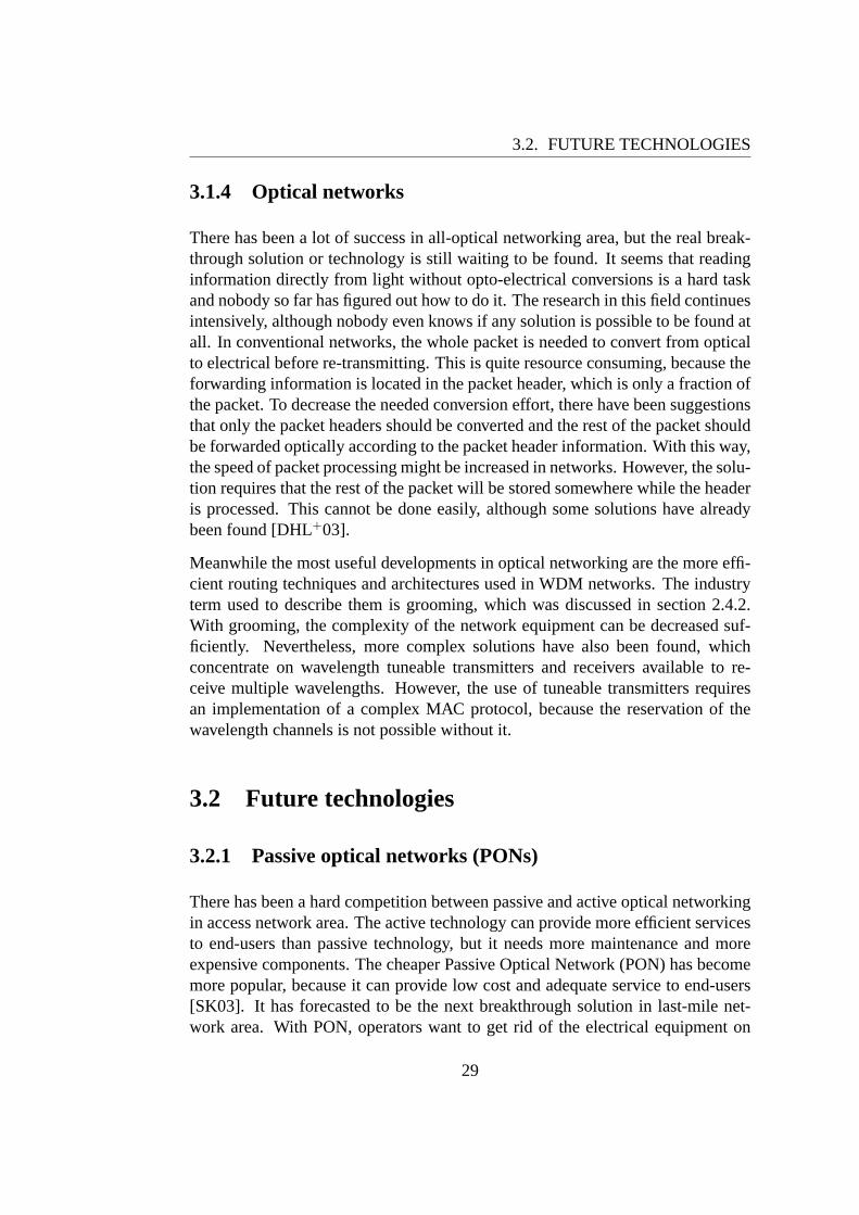
3.2.1 Passive optical networks (PONs)
There has been a hard competition between passive and active optical networkingin access network area. The active technology can provide more efficient servicesto end-users than passive technology, but it needs more maintenance and moreexpensive components. The cheaper Passive Optical Network (PON) has becomemore popular, because it can provide low cost and adequate service to end-users[SK03]. It has forecasted to be the next breakthrough solution in last-mile net-work area. With PON, operators want to get rid of the electrical equipment on
29
3.2. FUTURE TECHNOLOGIES
Transmitter
transmitter
Receiver
1 x N
Arraywaveguidegrating(AWG)
DWDM
Multi − λλ1, λ2,...λ16
λ17,λ18...λ32
Downsream
Upstream
WDMA architecture
Receiver
Transmitter
Receiver
Transmitter
λ1
λ16
λ17
λ32
TDMA downstream
CO/POP
Subscriber
TDMA upstream
CO/POP
Subscriber
CBA
OLT
A B CONT−A A
BONT−BCBA
CONT−CCBA
CBA
OLT
AONT−A
ONT−B
ONT−C
B
C
B
A
C
Downsream
15XXnm
15XXnm
1300nm
1300nm
15XXnm
1300nmUpstream
TDMA architecture
Receiver
Receiver
Transmitter1 x NPassiveopticalpower splitter
15XXnmtransmitter
1300nmReceiver
Figure 3.2: The architecture and principle of TDMA and WDMA PONs, adoptedfrom [Com01].
the access network, which has requirements for electrical power and active parts.PON brings the optical network closer to end-users, providing more and cheaperbandwidth for households.
Depending on where the PON terminates, the system can be called Fiber-to-the-x (FTTx), where x can be: C (Curb), B (Building) or H (Home). PON can usesingle or multiple fibres for upstream and downstream traffic, with or withoutWDM. The principle of PON is to share the CO equipment and the feeder fibreamong as many Optical Network Terminals (ONTs) as possible. This is illustratedin figure 3.2, where the architectures and principles of Time Division MultipleAccess (TDMA) and Wavelength Division Multiple Access (WDMA) PONs arepresented [Com01].
The establishment of Full Service Access Networks (FSAN) consortium was thefirst activity in PON area [Net02]. Its goal was to define a common standardfor PON technology, which was the ATM Passive Optical Network (APON), an-nounced in 1995 and later renamed to Broadband PON (BPON) [KP02]. Thenyears passed and the activity in PON area started again in November 2000, when
30

3.2. FUTURE TECHNOLOGIES
the Ethernet in the First Mile (EFM) task force was established by the Instituteof Electrical and Electronics Engineers (IEEE) [SK03]. They were concentrat-ing on standardising a 1.25 Gbps symmetrical PON system for Ethernet transportonly. Then as an answer to the EFM’s aims on Gb area, the FSAN released theGb PON (GPON) recommendation [ITU02]. Meanwhile the work in EFM groupwas concentrated on developing the Ethernet PON (EPON), which is still underdevelopment. All of the different PON technologies are presented in the followinglist.
• ATM based PON (APON)— APON was the first PON system and it usesATM as its bearer protocol. Later it was renamed to BPON, because fromthe name APON, people assumed that ATM services could be provided toend users, which was not the truth. Now the name BPON reflects the of-fering of broadband services, including Ethernet access, video distributionand high-speed leased line services. APON system has typical ATM likeperformance, including large overhead and low scalability with short delaysand reliable operation [Net02].
• Broadband PON (BPON) — This is the presently used name for APONand it is based on ITU-T recommendations G.983.1 [IT98], G.983.2 [IT00d]and G.983.3 [IT01a].
• Ethernet based PON (EPON)— This is IP efficient and low cost PON,based on Ethernet technology. It supports voice transport together with datatransport. EPON is scalable, but not so efficient in voice transfer [KP02].
• Gigabit PON (GPON) — This is an ITU-T recommendation for PON ser-vice requirements for speeds over 1 Gbps. GPON provides high bit rate sup-port enabling the transport of multiple services in native formats and withhigh efficiency, especially data and TDM. It is the native PON and standsas a foundation for new PONs, not based on APON. In addition, GPONsupports ITU-T standard Generic Framing Procedure (GFP) mapping andprovides the best efficiency in voice and data transportation [Net02].
• WDM-PON — The name DWDM- or WDM-PON is used for PONs, wheremultiple wavelengths are used. This requires the use of more expensiveoptical equipment, but enables higher bandwidth [Com01].
One important factor in PONs is the variety of architectures and topologies wherethey can be used in the network. With this flexibility, the PON can be implementedalmost everywhere easily. However, the physical tree, logical star topology seems
31

3.2. FUTURE TECHNOLOGIES
to be the most suitable for PONs [GCC92]. Scalability and security issues arealso important. With a scalable system the bursts in traffic can be balanced andbandwidth increased easily. Furthermore, when all downstream traffic is sent toeveryone in the network, like it is in TDMA PON system, encryption mechanismsare necessary to provide the minimum-security [KP02].
3.2.2 Resilient Packet Ring (RPR)
The Resilient Packet Ring (RPR) standard [Gro03] defines a data optimised net-work, providing both legacy TDM and differentiated packet-based services. Thedevelopment of RPR started from the need to combine the advantages of bothSDH and Ethernet. The RPR standard supports ring topology and fast protectionmechanisms, exclusive to SDH, together with data efficiency, simplicity and costadvantages, exclusive to Ethernet. It is a multi-service transport protocol based onpackets rather than circuits. Because of this, it can use the ring topology more ef-ficient than SDH [All03]. RPR has also support for multicast and broadcast traffictogether with VPN, which is emerging among companies worried about their datasecurity.
RPR is a OSI-layer two Medium Access Control (MAC) protocol, supportingQoS in three different priority levels: high, medium and low. High priority ser-vice supports applications that require bandwidth guarantees and tightly boundeddelay and jitter specifications (voice, video and circuit emulation applications).Medium priority applications are not sensitive for delay, but require bandwidthcommitment. Low priority is for the best-effort traffic. The fairness control al-gorithm is responsible for the negotiation of bandwidth between stations and itis also used in congestion avoidance. In RPR, the nodes share the same multic-ast message and can strip unicast packets from their destination, achieving spatialreuse or bandwidth multiplication [All01].
RPR can operate together with SDH and 1 or 10Gb Ethernet, bringing ring topo-logy’s efficient protection available for Gb Ethernet. RPR operates with at leasttwo counter-rotating rings available to transport working traffic. The automatictopology discovery is responsible for the network configuration, enabling auto-matic updates when the network structure is changed. Wrapping and steering arethe protection methods used in RPR and illustrated in figure 3.3. These protectionmethods allow the restoration of operations in the limit of 50 ms, which is thedesired level commonly known in networking [All03].
32
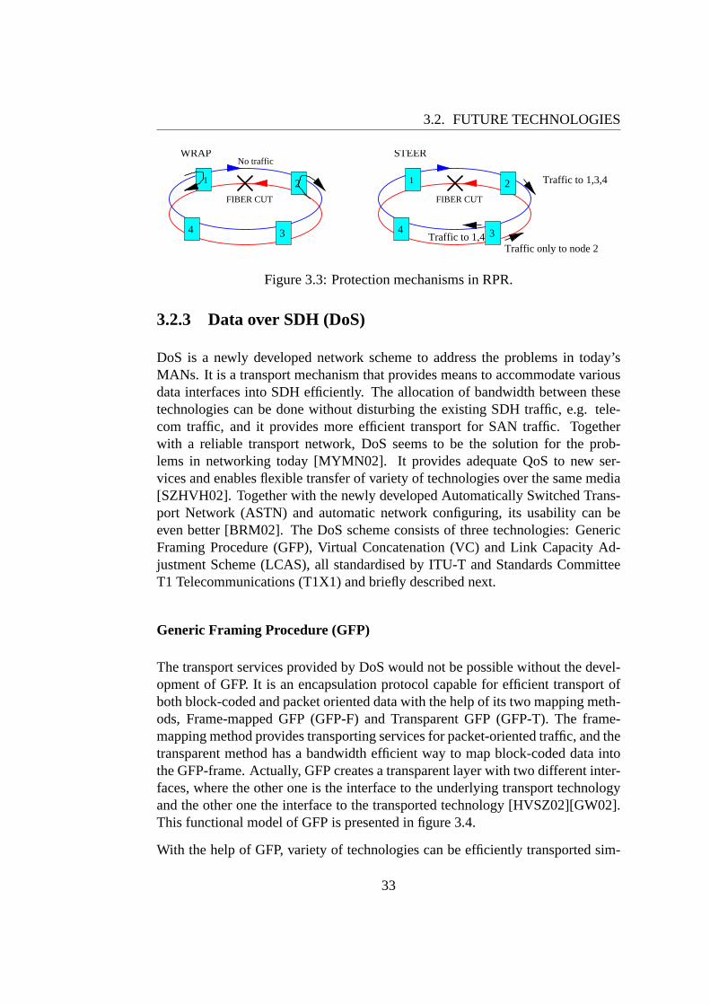
3.2. FUTURE TECHNOLOGIES
FIBER CUT
Traffic to 1,4Traffic only to node 2
Traffic to 1,3,4
STEERWRAPNo traffic
FIBER CUT
34
21
34
21
Figure 3.3: Protection mechanisms in RPR.
3.2.3 Data over SDH (DoS)
DoS is a newly developed network scheme to address the problems in today’sMANs. It is a transport mechanism that provides means to accommodate variousdata interfaces into SDH efficiently. The allocation of bandwidth between thesetechnologies can be done without disturbing the existing SDH traffic, e.g. tele-com traffic, and it provides more efficient transport for SAN traffic. Togetherwith a reliable transport network, DoS seems to be the solution for the prob-lems in networking today [MYMN02]. It provides adequate QoS to new ser-vices and enables flexible transfer of variety of technologies over the same media[SZHVH02]. Together with the newly developed Automatically Switched Trans-port Network (ASTN) and automatic network configuring, its usability can beeven better [BRM02]. The DoS scheme consists of three technologies: GenericFraming Procedure (GFP), Virtual Concatenation (VC) and Link Capacity Ad-justment Scheme (LCAS), all standardised by ITU-T and Standards CommitteeT1 Telecommunications (T1X1) and briefly described next.
Generic Framing Procedure (GFP)
The transport services provided by DoS would not be possible without the devel-opment of GFP. It is an encapsulation protocol capable for efficient transport ofboth block-coded and packet oriented data with the help of its two mapping meth-ods, Frame-mapped GFP (GFP-F) and Transparent GFP (GFP-T). The frame-mapping method provides transporting services for packet-oriented traffic, and thetransparent method has a bandwidth efficient way to map block-coded data intothe GFP-frame. Actually, GFP creates a transparent layer with two different inter-faces, where the other one is the interface to the underlying transport technologyand the other one the interface to the transported technology [HVSZ02][GW02].This functional model of GFP is presented in figure 3.4.
With the help of GFP, variety of technologies can be efficiently transported sim-
33
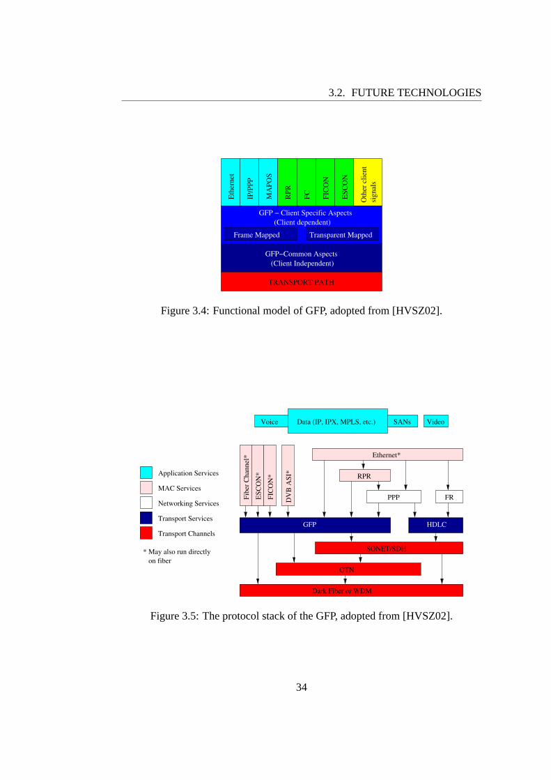
3.2. FUTURE TECHNOLOGIES
IP/P
PP
MA
POS
RPR
FC FIC
ON
ESC
ON
Eth
erne
t
GFP − Client Specific Aspects (Client dependent)
GFP−Common Aspects (Client Independent)
TRANSPORT PATH
Frame Mapped Transparent Mapped
Oth
er c
lient
sign
als
Figure 3.4: Functional model of GFP, adopted from [HVSZ02].
Application Services
MAC Services
Networking Services
Transport Services
Transport Channels
SONET/SDH
Dark Fiber or WDM
OTN
GFP HDLC
FR
RPR
Data (IP, IPX, MPLS, etc.)Voice SANs Video
DV
B A
SI*
FIC
ON
*
ESC
ON
*
Fibe
r Cha
nnel
* Ethernet*
PPP
* May also run directly on fiber
Figure 3.5: The protocol stack of the GFP, adopted from [HVSZ02].
34

3.2. FUTURE TECHNOLOGIES
ultaneously over the same transport media. These technologies are presented infigure 3.5, where the location of GFP in the protocol stack is also illustrated. Inthe future the number of technologies supported by GFP will increase with highprobability, especially, if the DoS scheme is adopted by the industry. At thispoint, it seems that DoS will be implemented widely, because it can use the exist-ing fibre infrastructure, and only the networking equipment need to be changed.So the costs for the implementation of DoS will be low, compared to other newtechnologies. In addition, GPON already has a support for GFP [Net02].
Virtual Concatenation (VC)
One weakness of SDH has been the lack of efficient allocation of bandwidth,which is very important for operators in today’s networking. With efficient al-location methods operators can have better bandwidth utilisation together withimproved service supply for their customers. In modern Ethernet links, the al-location of bandwidth can be changed very quickly with fine granularity. Thishas increased the competition between SDH and Ethernet in the metro and longhaul networks. The situation is about to change with the new SDH networkingequipment, supporting Virtual Concatenation (VC) and Link Capacity AdjustmentScheme (LCAS) [OSG02].
Table 3.1: The efficiency of virtual concatenation compared to contiguous con-catenation. In the table, the acronym VC means Virtual Container, adopted from[HV02].
Contiguous Concatenation Virtual Concatenation
10 Mb/s Ethernet: VC-3 (20%) VC-12-12v (92%)100 Mb/s Ethernet: VC-4 (67%) VC-3-2v (100%)1 Gb/s Ethernet: VC-4-16c (42%) VC-4-7v (95%)
The basic principle of VC is quite simple. A number of smaller containers areconcatenated and assembled, to create a bigger container that carries more dataper second. This technique provides four advantages compared to the legacy con-tiguous concatenation used in conventional SDH networks: scalability, efficiency,compatibility and resiliency [OSG02]. More scalability and efficiency is achievedwith smaller granularity as presented in table 3.1. VC works in legacy networksas well, and more compatibility is achieved by transporting data channels over oldnetworks that do not support large contiguous channels at all. Furthermore, indi-
35

3.3. RECENT RESEARCH PROJECTS
vidual members of a virtually concatenated channel are routed diversely, provid-ing more resiliency for the transfer.
Link Capacity Adjustment Scheme (LCAS)
The bandwidth allocation with Virtual Concatenation (VC) is done only when thespecific channel is configured. It doesn’t have monitoring or adjustment functionsto address the changes in traffic flow. LCAS is designed for this specific purposeand it can operate only together with VC. With LCAS the allocated channel sizescan be changed at any time without disturbing the traffic on the link. In addition,connectivity checks are performed continuously and failed links restored withoutintervention of the management software. Furthermore, LCAS can detect if thereserved channel is utilised wholly or not. If there is unused bandwidth reservedfor a certain channel, LCAS can adjust the channel and give the extra bandwidthfor others to use. In the same way it can also increase the capacity of the channel[OSG02].
3.3 Recent research projects
The research in communication area still continues despite of the recession in IT-industry. Today, several research projects are concentrating on metropolitan areanetworking. The main targets of the MAN development were already discussedearlier in this chapter and now a few of the recent research projects are presented.All of them concentrate on different sides of the metropolitan area networking.HARMONICS-project concentrates on access network developing and its goal isto create a WDM-PON system to be utilised in the last-mile networks. The MANtransport area is investigated in the project called IP-HORNET, where the goal isto develop a ring structured, WDM-based metropolitan transport network. Andthe core network side of the MAN is studied in the project called DAVID, wherethe goal is to develop a common packet-over-WDM transport solution for bothMAN and WAN.
3.3.1 HARMONICS
Hybrid Access Reconfigurable Multi-wavelength Optical Networks for IP-basedCommunication Systems (HARMONICS) is a research project running from May
36
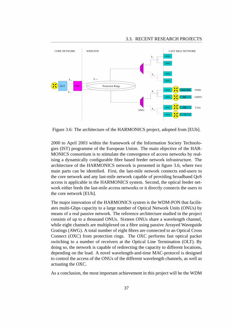
3.3. RECENT RESEARCH PROJECTS
λ N
λ 1
Coax
UMTS
VDSL
?
λ
λ
1
NAWG
CORE NETWORK WDM PON LAST MILE NETWORK
λ λ
λ
1−Z
Y
X
Protection Rings
DSLAM
BS
HE
OXCOLT
ONU
ONU
ONU
ONU
ONU
ONU
ONU
ONU
Figure 3.6: The architecture of the HARMONICS project, adopted from [EUb].
2000 to April 2003 within the framework of the Information Society Technolo-gies (IST) programme of the European Union. The main objective of the HAR-MONICS consortium is to stimulate the convergence of access networks by real-ising a dynamically configurable fibre based feeder network infrastructure. Thearchitecture of the HARMONICS network is presented in figure 3.6, where twomain parts can be identified. First, the last-mile network connects end-users tothe core network and any last-mile network capable of providing broadband QoSaccess is applicable in the HARMONICS system. Second, the optical feeder net-work either feeds the last-mile access networks or it directly connects the users tothe core network [EUb].
The major innovation of the HARMONICS system is the WDM-PON that facilit-ates multi-Gbps capacity to a large number of Optical Network Units (ONUs) bymeans of a real passive network. The reference architecture studied in the projectconsists of up to a thousand ONUs. Sixteen ONUs share a wavelength channel,while eight channels are multiplexed on a fibre using passive Arrayed WaveguideGratings (AWG). A total number of eight fibres are connected to an Optical CrossConnect (OXC) from protection rings. The OXC performs fast optical packetswitching to a number of receivers at the Optical Line Termination (OLT). Bydoing so, the network is capable of redirecting the capacity to different locations,depending on the load. A novel wavelength-and-time MAC-protocol is designedto control the access of the ONUs of the different wavelength channels, as well asactuating the OXC.
As a conclusion, the most important achievement in this project will be the WDM
37
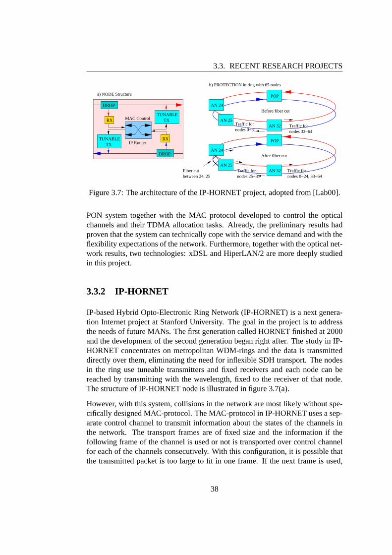
3.3. RECENT RESEARCH PROJECTS
IP Router
MAC Control
a) NODE Structure
RX
DROP
TUNABLE TXRX
DROP
TUNABLE TX
Before fiber cut
After fiber cut
Fiber cutbetween 24, 25
Traffic fornodes 0−31
Traffic fornodes 25−31
nodes 33−64Traffic for
nodes 0−24, 33−64Traffic for
b) PROTECTION in ring with 65 nodes
AN 25AN 32
POP
AN 24
AN 25
AN 24
POP
AN 32
Figure 3.7: The architecture of the IP-HORNET project, adopted from [Lab00].
PON system together with the MAC protocol developed to control the opticalchannels and their TDMA allocation tasks. Already, the preliminary results hadproven that the system can technically cope with the service demand and with theflexibility expectations of the network. Furthermore, together with the optical net-work results, two technologies: xDSL and HiperLAN/2 are more deeply studiedin this project.
3.3.2 IP-HORNET
IP-based Hybrid Opto-Electronic Ring Network (IP-HORNET) is a next genera-tion Internet project at Stanford University. The goal in the project is to addressthe needs of future MANs. The first generation called HORNET finished at 2000and the development of the second generation began right after. The study in IP-HORNET concentrates on metropolitan WDM-rings and the data is transmitteddirectly over them, eliminating the need for inflexible SDH transport. The nodesin the ring use tuneable transmitters and fixed receivers and each node can bereached by transmitting with the wavelength, fixed to the receiver of that node.The structure of IP-HORNET node is illustrated in figure 3.7(a).
However, with this system, collisions in the network are most likely without spe-cifically designed MAC-protocol. The MAC-protocol in IP-HORNET uses a sep-arate control channel to transmit information about the states of the channels inthe network. The transport frames are of fixed size and the information if thefollowing frame of the channel is used or not is transported over control channelfor each of the channels consecutively. With this configuration, it is possible thatthe transmitted packet is too large to fit in one frame. If the next frame is used,
38

3.3. RECENT RESEARCH PROJECTS
information about an incomplete packet is included in the last byte of the frameand the transmitting of this packet continues when the next free frame is found inthe same channel [Lab00]. Furthermore, the protection in IP-HORNET is carriedout in a way that after fibre cut, the network is reconfigured to transport the trafficover existing routes, as depicted in figure 3.7(b). In the worst case, the perform-ance of the network is the same as before the fibre cut and the restoration time isthe same as the propagation delay in the fibre1 [Lab00].
One of the results of the IP-HORNET project was the development of new archi-tecture for the next generation metropolitan area network. With this architecture,the network infrastructure costs can be dramatically decreased compared to con-ventional networks. However, because of this structure, specific MAC and fairnessprotocols were needed to develop. This brings more costs to the design, but it isstill cheaper than conventional solutions. A new survivability scheme was de-veloped, providing full survivability after one fibre cut or node failure. The maindevelopments were a new suite of protocols and the three new subsystems, a fast-tuneable packet transmitter, an asynchronous packet receiver and a linear opticalamplifier [Lab00].
3.3.3 DAVID
The Data and Voice Integration over DWDM (DAVID) project contributes tokey action IV of IST on "Essential Technologies and Infrastructure". The mainobjective is to propose a packet-over-WDM network solution, including traffic-engineering capabilities and network management, covering the entire area fromMAN to WAN. The project will utilise optics as well as electronics in order to findthe optimum mix of technologies for future very-high-capacity networks. In themetropolitan area region, the focus is on implementing MAC protocol for opticalMANs. In the wide area region, the architecture of the project is multilayered, em-ploying packet switched domains containing electrical and optical packet switchesas well as wavelength routed domains [EUa].
The architecture of the DAVID network demonstrator is presented in figure 3.8,where the WAN consists of connected Optical Packet Routers (OPRs) and theMANs from several ring networks, which can share the same physical network.These ring networks, which consist of Optical Packet Add/Drop Multiplexers(OPADMs), are connected to the core network through a HUB. These networkshave a unified control system called the Multi Protocol Label Switching (MPLS).
1Less than 1ms in a typical MAN.
39

3.3. RECENT RESEARCH PROJECTS
MANMAN
WAN
HUB
OPADMOPADM
OPADM
HUB
OPADM
OPADM
OPADM
OPR
OPROPR
OPROPR
GATEWAY GATEWAY
Figure 3.8: The outline of the DAVID project demonstrator, adopted from [EUa].
The duration of the DAVID project is from July 2000 to July 2003 and the resultsof the project have not been fully revealed yet. However, some of the findingscan already be mentioned. First of all, optical networking is on its way, but stillexpensive. Second, the IP-over-DWDM solution for high capacity networks isnot likely to be flexible, because IP is not as suitable a solution as single data-transport technology in the core network. And last, IP will be an important clientlayer interface for many years, especially when it can be the integrator for efficientcontrol structures like MPLS and Generic MPLS (GMPLS) [EUa].
3.3.4 Discussion
All of the projects presented here concentrated on metropolitan area WDM net-working. In this area, dynamic wavelength allocation is the most popular method,although the utilisation of dynamic channels needs the implementation of theMAC-protocol [Ben02]. In addition, static wavelength-channels can be used to-gether with dynamic channels. The ring network seems to be the most desiredphysical topology for the metropolitan feeder network, because of the protec-tion capabilities it provides. Some studies concentrate on standards, which havealready been developed or are under development, but others concentrate on find-ing new ways, which might be developed into standards later. The last-mile net-work will develop towards passive optical network solution, which can be seenfrom the number of solutions available in that area.
40
Chapter 4
Research project OAN
Optical Access Networking (OAN) is a TEKES-funded research project whereVTT1 Microelectronics, VTT Information technology and HUT2 Networking labor-atory together with few private businesses are participating. The duration of theproject is three years and it will end in December 2003. The goal in OAN isto study metropolitan area networking, find the future requirements and develop-ment directions of that area and based on the results, eventually build a networkdemonstrator. The work is divided between different institutes in a way that theHUT Networking laboratory is responsible for the traffic modelling and algorithmdevelopment, the VTT Microelectronics is responsible for the implementation ofthe optical transport network and the VTT Information technology is responsiblefor the implementation of electrical parts and controlling software for the demon-strator.
4.1 OAN test network architecture
After some study in the metropolitan area networking, it came clear that the mostusable and later expandable solution for the OAN demonstrator should be basedon standards. In that time, the scheme called DoS was gaining great favour amongspecialists and when it was to be standardised, it was selected as the main archi-tecture for the OAN test network. In addition to standardisation, DoS has otherstrengths as well. These were already discussed in chapter 3 and were notifiedin the final network architecture decision. The most important strengths were the
1Technical Research Centre of Finland (VTT)2Helsinki University of Technology (HUT)
41
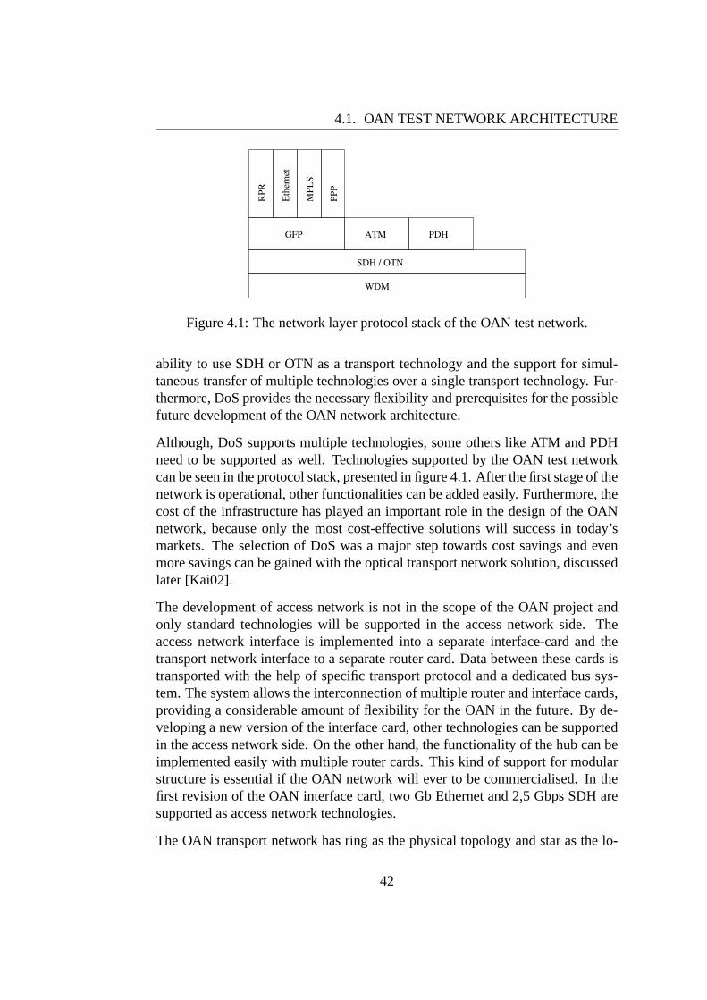
4.1. OAN TEST NETWORK ARCHITECTURE
SDH / OTN
WDM
PDH
PPP
MPL
S
RPR
Eth
erne
t
GFP ATM
Figure 4.1: The network layer protocol stack of the OAN test network.
ability to use SDH or OTN as a transport technology and the support for simul-taneous transfer of multiple technologies over a single transport technology. Fur-thermore, DoS provides the necessary flexibility and prerequisites for the possiblefuture development of the OAN network architecture.
Although, DoS supports multiple technologies, some others like ATM and PDHneed to be supported as well. Technologies supported by the OAN test networkcan be seen in the protocol stack, presented in figure 4.1. After the first stage of thenetwork is operational, other functionalities can be added easily. Furthermore, thecost of the infrastructure has played an important role in the design of the OANnetwork, because only the most cost-effective solutions will success in today’smarkets. The selection of DoS was a major step towards cost savings and evenmore savings can be gained with the optical transport network solution, discussedlater [Kai02].
The development of access network is not in the scope of the OAN project andonly standard technologies will be supported in the access network side. Theaccess network interface is implemented into a separate interface-card and thetransport network interface to a separate router card. Data between these cards istransported with the help of specific transport protocol and a dedicated bus sys-tem. The system allows the interconnection of multiple router and interface cards,providing a considerable amount of flexibility for the OAN in the future. By de-veloping a new version of the interface card, other technologies can be supportedin the access network side. On the other hand, the functionality of the hub can beimplemented easily with multiple router cards. This kind of support for modularstructure is essential if the OAN network will ever to be commercialised. In thefirst revision of the OAN interface card, two Gb Ethernet and 2,5 Gbps SDH aresupported as access network technologies.
The OAN transport network has ring as the physical topology and star as the lo-
42

4.2. OAN TEST NETWORK PROTOTYPE
gical topology. These are selected because the ring structure has efficient protec-tion capabilities and the tree structure is cost effective. The OAN network attemptsto fulfil all the requirements for future MANs, presented in chapter 3. The sup-port for these functionalities is mainly based on DoS and in other functionalitiessupported by it. Furthermore, the OAN network utilises automatic configurationand Automatically Switched Transport Network (ASTN), and the managementof the network is carried out with a standardised network management protocol,Simple Network Management Protocol (SNMP). However, at the first stage ofthe OAN test network implementation, only DoS will be implemented and otherfunctionalities, like VPN, are left for later implementation.
4.2 OAN test network prototype
Prototype implementation is an important part of device centric development.With a fully functional prototype, early research conclusions can be tested andverified. Usually, the faults in the design development can be seen in this stageonly. The first OAN prototype is planned strictly for testing purposes, and it willbe used to test different metropolitan area networking schemes. The functional-ity of the prototype can be modified or increased whenever necessary, and theseimprovements can be easily verified right after implementation. This flexibility inthe design is provided with Field Programmable Gate Arrays (FPGAs), which areresponsible for most of the network functionality. The functionality of the FPGAis carried out with a specific program, downloadable to the chip. New programscan be downloaded to the chip whenever there is need to change the functionalityof the FPGA. The OAN prototype has three different FPGAs, which provide re-latively large amount of programmability, compared to the use of programmablelogic today. Furthermore, these FPGAs have a great number of connection pointsand every important chip in the prototype is connected to them.
The implementation of the OAN prototype will be executed in co-operation betweenVTT Information Technology and VTT Microelectronics, which both have theirown responsibility area in the project. VTT Information Technology is responsiblefor the design and implementation of the electrical part of the network, includingall of the networking activities, starting from the link layer. VTT Microelectronicsis responsible for the implementation of the transport network, which is a WDMnetwork with optical protection. The physical equipment of the OAN node isfit into a standard CompactPCI-frame, which makes the node easy to install andmove. The CompactPCI-frame includes a Central Processing Unit (CPU) card,which is used by the management software.
43

4.2. OAN TEST NETWORK PROTOTYPE
I/OROUTER
Gb Ethernet
Gb Ethernet
FPGA
FPGADATA
CONTROL
PCI
SRAM
SerD
esSe
rDes
SDH
SDH
SDH
LASERCTRL
COUNTER−ROTATINGSDH RINGS
FPGA
Figure 4.2: Simplified architecture of the OAN test network prototype node.
4.2.1 Functionality of the node
The design of the OAN prototype router and interface cards started with the iden-tification of necessary supporting functions and interfaces. These were the controlinterface towards CPU, laser controller, test Light Emitting Diodes (LEDs), testpoints, connections between cards and the power supply for the system. The CPUcan access the devices in the prototype through Peripheral Component Intercon-nect (PCI) bus. The interface is implemented with a specific PCI-interfacing chip.After the supporting functions were identified, it was time to specify the actualbenefit functions of the system, the network functions. In the network part, theprototype exploits two counter-rotating 2,5 Gbps SDH rings with Automatic Pro-tection Switching (APS) in the transport network side and two Gb Ethernet linkstogether with one 2,5 Gbps SDH link in the access network side. The simplifiedprototype layout is presented in figure 4.2, where the different devices togetherwith the connections between them are illustrated. Furthermore, the devices inthe OAN prototype are presented in more detail in table 4.1.
SDH framing is a fully standardised procedure and there are several dedicatedchips available for the purpose. In OAN prototype, the PMC-Sierra producedPM5381 chip was selected to be the SDH framer in both, router and interface (I/O)cards. To fully exploit the possibilities provided by Sierra’s SDH chip, specific
44

4.2. OAN TEST NETWORK PROTOTYPE
Table 4.1: Devices attached to the OAN prototype node.
Type Manufacturer Location Function
XC2V1000 Xilinx Inc. I/O FPGAXC2V2000 Xilinx Inc. Router FPGAXC2V6000 Xilinx Inc. Router FPGAPM3386 PMC-Sierra I/O 2x Gb EthernetPM5310 PMC-Sierra Router TelecomBus serialiser/deserialiserPM5381 PMC-Sierra Router&I/O 2,5 Gb/s SDH/SONET framer/deframerPCI9030 PLX Technology Router Interface to PCI
TelecomBus serialises were needed to access the TelecomBus-line of the SDH-chips. With TelecomBus, the SDH data flow can be accessed with byte by bytebasis, which is necessary for the DoS functionality. These serialises were PMC-Sierra’s PM5310-chips, which are connected into the smaller FPGA (XC2V2000)in the router card. Furthermore, the smaller FPGA is connected to the largerFPGA (XC2V6000). The control channel from PCI, additional Static RandomAccess Memory (SRAM) together with the laser controller equipment are all con-nected to this FPGA as well. The interface card has only one FPGA (XC2V1000)and two PMC-Sierra’s chips. One is the SDH framer and the other is a two portGb Ethernet (PM3386). Both of these chips are connected to the FPGA, which isfurther connected to the larger FPGA in route-card.
4.2.2 Network structure
To keep the network complexity low, the OAN prototype network consists ofonly three to four nodes. One of the nodes works as a hub, connecting all of theother nodes to the core network and to each other. These connections are carriedout with the help of WDM technology using Wavelength Add Drop Multiplex-ers (WADMs). With WADMs, all the nodes can strip their specific wavelengthfrom the ring and by using wavelength tuneable transmitters, every node can havea single light path to the hub and back. This structure is depicted in figure 4.3(a),and its purpose is to avoid complexity and reduce the amount of intelligence inthe network. In other words, the most desirable solution for the network would bephysical ring — logical ring, where every node would have the ability to transmitdata directly to all of the other nodes. However, this solution demands expens-ive wavelength converters to be installed in every node, together with a complexnetwork management protocol. Because the most of the traffic in MAN is trans-mitted from or to backbone network, the more appropriate solution for the MAN
45
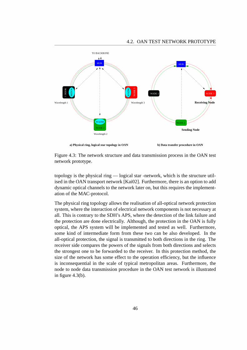
4.2. OAN TEST NETWORK PROTOTYPE
b) Data transfer procedure in OANa) Physical ring, logical star topology in OAN
Sending Node
Receiving Node
Wavelength 2
Wavelength 1 Wavelength 3
TO BACKBONE
NODE 2
NO
DE
1
HUB
NODE 2
NODE 1 NODE 3
HUB
NO
DE
3
WADM
WA
DM
WA
DM
Figure 4.3: The network structure and data transmission process in the OAN testnetwork prototype.
topology is the physical ring — logical star -network, which is the structure util-ised in the OAN transport network [Kai02]. Furthermore, there is an option to adddynamic optical channels to the network later on, but this requires the implement-ation of the MAC-protocol.
The physical ring topology allows the realisation of all-optical network protectionsystem, where the interaction of electrical network components is not necessary atall. This is contrary to the SDH’s APS, where the detection of the link failure andthe protection are done electrically. Although, the protection in the OAN is fullyoptical, the APS system will be implemented and tested as well. Furthermore,some kind of intermediate form from these two can be also developed. In theall-optical protection, the signal is transmitted to both directions in the ring. Thereceiver side compares the powers of the signals from both directions and selectsthe strongest one to be forwarded to the receiver. In this protection method, thesize of the network has some effect to the operation efficiency, but the influenceis inconsequential in the scale of typical metropolitan areas. Furthermore, thenode to node data transmission procedure in the OAN test network is illustratedin figure 4.3(b).
46

Chapter 5
FPGA programming methodology
There are number of issues involved in the Hardware Description Language (HDL)design, especially if it is targeted to FPGAs. These issues together with the designmethodology and implementation procedures are presented and briefly discussedin this chapter. The purpose of this discussion is to provide basic knowledgeabout the FPGA programming. In the programming process, desired functionalit-ies are first described with a specific programming language and then downloadedinto the FPGA device. The description languages used in HDL-programming areVHSIC Hardware Description Language (VHDL) and Verilog. Writing of the de-scription, i.e., programming, can be done by an individual or several programmers,depending on the size and implementation time of the design. All programmers,as individuals, have their unique way to create code. Usually, the variety in codingstyles is not desirable, especially if there is a need to make modifications or usethe code afterwards. For that reason, clear coding principles and rules for opera-tions are necessary for the programmers. This is the only way to get more unifiedcode, the functionality of which can be easily understood.
5.1 FPGA basics
The FPGAs today provide lots of flexibility into the designs and for that reason,they are coming more and more popular among hardware designers. The flex-ibility comes from the possibility to program the chips over and over again anddecreases the number of re-designing stages in prototype manufacturing. There-programmability provides advantages compared to the Application Specific In-tegrated Circuit (ASIC) chips, which ones ruled the market. Opposite to the ASIC,
47
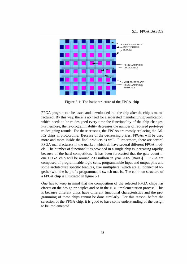
5.1. FPGA BASICS
PROGRAMMABLEINPUT/OUTPUTBLOCKS
PROGRAMMABLELOGIC CELLS
PROGRAMMABLESWITCHES
WIRE MATRIX AND
Figure 5.1: The basic structure of the FPGA-chip.
FPGA program can be tested and downloaded into the chip after the chip is manu-factured. By this way, there is no need for a separated manufacturing verification,which needs to be re-designed every time the functionality of the chip changes.Furthermore, the re-programmability decreases the number of required prototypere-designing rounds. For these reasons, the FPGAs are mostly replacing the AS-ICs chips in prototyping. Because of the decreasing prices, FPGAs will be usedmore and more inside the final products as well. Furthermore, there are severalFPGA manufacturers in the market, which all have several different FPGA mod-els. The number of functionalities provided in a single chip is increasing rapidly,because of the hard competition. It has been forecasted that the gate count inone FPGA chip will be around 200 million in year 2005 [Bai03]. FPGAs arecomposed of programmable logic cells, programmable input and output pins andsome architecture specific features, like multipliers, which are all connected to-gether with the help of a programmable switch matrix. The common structure ofa FPGA chip is illustrated in figure 5.1.
One has to keep in mind that the composition of the selected FPGA chips haseffects on the design principles and so in the HDL implementation process. Thisis because different chips have different functional characteristics and the pro-gramming of these chips cannot be done similarly. For this reason, before theselection of the FPGA chip, it is good to have some understanding of the designto be implemented.
48

5.2. HDL-IMPLEMENTATION PROCESS
5.2 HDL-implementation process
The common HDL-implementation process consists of three aggregates, whichall have their own responsibility area in the process. These are design planningstage, implementation stage and verification stage. Implementation and verific-ation stages work together forming the design flow, where the result of the veri-fication determines if modifications to the code are needed or not. Sometimesre-writing the code is not adequate to fix the error and modifications to the designspecification may be needed as well.
5.2.1 Design planning
The most important task in the implementation process is the creation of thedesign specification document. This is the most important document during thewhole implementation process and everything later on is based on the solutionspresented in here. The design specification document covers the functionality ofthe whole design. The specification starts from the overall architecture and pur-pose of the design and then moves deeper into details. Depending on the designfunctionalities, the architecture is partitioned into several blocks and sub-blocks.Then the functionality of each block is described with necessary technical details.Furthermore, all of the interfaces between design blocks need to be specified withdetail, so that combining of the blocks in the implementation stage would be asstraightforward as possible. The specification document must be prepared withgreat carefulness, because all mistakes made here have multiple effects on thelater implementation tasks.
5.2.2 Design flow
The coding of design blocks may begin after the design specification document isready. The coding of components is only a part of the whole HDL design flow,which consist of several operations. These operations test, simulate and modifythe code, forming the final FPGA specific version of the program. The designflow from the Xilinx point of view [Inc03] is presented in figure 5.2.
In the design flow, the code is verified and fixed as many times as it is necessaryto fulfil the requirements stated in the specification document. After this, thecode is synthesised and the correctness of the synthesis process is validated withsimulation. Then the synthesised design is converted in the FPGA specific form,
49

5.2. HDL-IMPLEMENTATION PROCESS
AnalysisTiming
Simulation
Design Verification
FunctionalSimulation
Static Timing
VerificationIn−Circuit
AnnotionBack
SynthesisDesign
DesignEntry
Download toa Device
ImplementationDesign
Figure 5.2: The HDL design flow according to Xilinx, adopted from [Inc03].
where timing simulation and static timing analysis can be done. If the timinganalysis is not passed, some modifications to the design will be needed. Afterthe analysis is passed, this FPGA specific form of the code can be downloadedinto the FPGA-chip. The final functionality of the chip can then be validated within-circuit validation.
5.2.3 Verification
The verification of the design can be performed in several hierarchical levels, atthe same time with the design integration. By this way, different abstractions ofthe code can be verified efficiently. The validation is only responsible for verifyingthe functionality of the final design, and it does not test the functionality of theblocks with the same detail as it is possible in hierarchical verification. Validationis important, but it is not as good in locating errors as the hierarchical verification.Verification includes a lot of debugging. Debugging means that after a verificationerror, the code is fixed and then verified again as long as there are errors in thecode. However, it is nearly impossible to define such a verification process orsystem that all of the possible error combinations can be checked. For that reason,there are always some errors left in the code when it is released to the market andusers of the program act as final testers. Partly, this has lead to a situation, wheremore and more testing is left for the final users. Programming companies have cutdown their manufacturing testing efforts and improved their supporting functions.With efficient support, problems in code can be fixed right after they have been
50

5.3. DESIGN GUIDELINES
Refine &Partition Smaller Blocks
Major Blocks
Sub−System
System
Integration &Verification
ValidationSpecification FEEDBACK
Figure 5.3: Verification as a part of design implementation process, adopted andmodified from [Bai03].
noticed, and even more testing responsibility can be left for the users.
The verification process is usually performed from bottom to top by starting frombounded functionalities or small blocks and then moving towards larger aggreg-ates, finally reaching the top level of the design. This is contrary to the processof creating the design specification document, where the refining and partitioningis done from top to bottom. The verification process as a part of implementationprocess is illustrated in figure 5.3. The verification process takes usually 50-70percent of the total design implementation time. For that reason, it is advisableto build a verification plan for the design [Ber00]. The verification plan is a spe-cification document, where the verification effort is specified. This includes theschedule and resources available for the verification, i.e. the personnel and theneeded time. The verification specification document is build from the designspecification document. Furthermore, in larger corporations implementation andverification might be done separately in different departments and then the veri-fication personnel prepare the verification specification.
5.3 Design guidelines
There are a variety of different matters advisable to consider before the actual im-plementation can be started. These matters are called coding guidelines and theywill help in creating clear design structures and understandable code, improv-ing re-usability of the code. Furthermore, reductions in the total implementationtime and in the possibility for functional problems can be achieved with goodcoding guidelines [Ope02]. Sufficient commenting and clear structure helps inunderstanding the functionality of the code. Furthermore, using common namingconventions throughout the design helps in identifying the different parts of thedesign or following certain signal through the architecture [Cor99].
51
5.4. DESIGN QUALITY
A great number of different data files are produced in the HDL-implementationprocess and to manage these files, a clear file structure is needed to create. Thisstructure is good to design already in the beginning of the project, so that all filesare in right places right from the start. Furthermore, the purpose for which thecode was produced has a big effect on the syntax of the code. The syntax canbe quite different depending on whether it is implemented for simulation or forsynthesis. In addition, the code can be produced in a technology specific wayand in a performance driven way. The syntax of the implemented code should bestated in the design specification document.
5.4 Design quality
The quality of the design consists of all of the former described attributes. Adesign of good quality can be achieved only with careful planning and with clearrules. The design rules together with the guidelines need to be set in the begin-ning of the design project. It is good to make a design schedule and allocate theresources, so that enough time can be reserved for each design stage. The im-plementation tools are needed to select beforehand and the interoperability of thetools tested. After all of the necessary preparations are done appropriately, it isgood to keep the implementation personnel informed for every changes and dif-ficulties in the process. Of course the actual implementation process is needed toperform with adequate carefulness and by skilful personnel, but the weight of thisfact can be relatively decreased with the former described preparations.
52

Chapter 6
HDL-design options
In this chapter, the design options for the OAN test network prototype FPGA pro-grams are discussed. Before the actual discussion, we need to have some know-ledge about the programmable architectures and their properties. For this reason,the architectures of the FPGAs together with the programming tools used in theimplementation stage are presented. The overall functionality of the design mustbe defined first and the options for the implementation can be identified only afterthat. These options concentrate on different ways to achieve the desired function-ality. By this way, all of the possible implementations can be compared and themost suitable one selected. Furthermore, with the help of this kind of contempla-tion, possible future development and functionality additions can be consideredbeforehand and possibly taken into consideration already in the first version of thedesign. This will help the future developments of the system.
6.1 Target architectures
The purpose in the OAN project is to implement as many of the test networkfunctionalities as possible inside the FPGAs to achieve flexibility and reusabilityfor the implementation. This purpose was clear already in the beginning of theproject and, for that reason, the requirements for the FPGAs to be attached inthe prototype were a large amount of programmable logic, a sufficient numberof input and output pins and adequate operation efficiency. At the time of theselection, the Xilinx manufactured Virtex-II architecture was the most superior insize and efficiency and was selected as the architecture for OAN FPGAs. Xilinxprovides the Virtex-II architecture in different chip sizes and the selection was
53
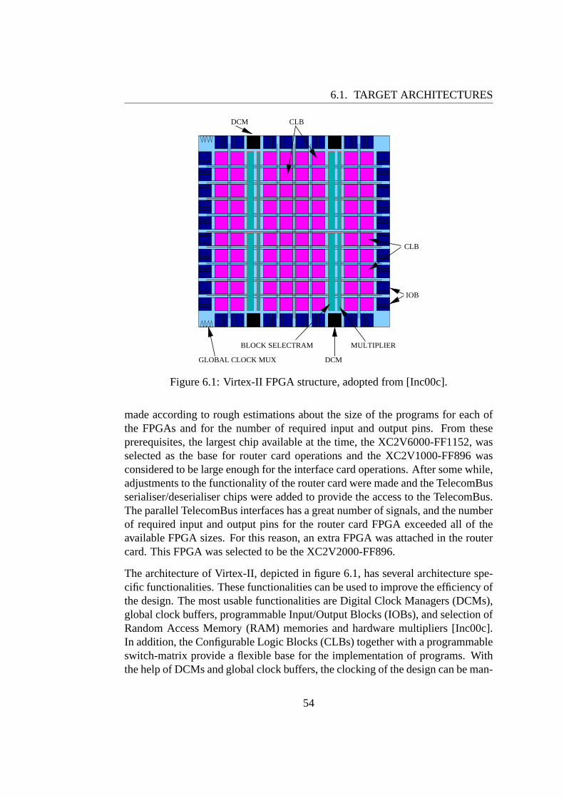
6.1. TARGET ARCHITECTURES
BLOCK SELECTRAM MULTIPLIER
DCMGLOBAL CLOCK MUX
CLB
IOB
CLBDCM
Figure 6.1: Virtex-II FPGA structure, adopted from [Inc00c].
made according to rough estimations about the size of the programs for each ofthe FPGAs and for the number of required input and output pins. From theseprerequisites, the largest chip available at the time, the XC2V6000-FF1152, wasselected as the base for router card operations and the XC2V1000-FF896 wasconsidered to be large enough for the interface card operations. After some while,adjustments to the functionality of the router card were made and the TelecomBusserialiser/deserialiser chips were added to provide the access to the TelecomBus.The parallel TelecomBus interfaces has a great number of signals, and the numberof required input and output pins for the router card FPGA exceeded all of theavailable FPGA sizes. For this reason, an extra FPGA was attached in the routercard. This FPGA was selected to be the XC2V2000-FF896.
The architecture of Virtex-II, depicted in figure 6.1, has several architecture spe-cific functionalities. These functionalities can be used to improve the efficiency ofthe design. The most usable functionalities are Digital Clock Managers (DCMs),global clock buffers, programmable Input/Output Blocks (IOBs), and selection ofRandom Access Memory (RAM) memories and hardware multipliers [Inc00c].In addition, the Configurable Logic Blocks (CLBs) together with a programmableswitch-matrix provide a flexible base for the implementation of programs. Withthe help of DCMs and global clock buffers, the clocking of the design can be man-
54

6.2. PROGRAMMING TOOLS
Table 6.1: The resources available in the prototype FPGAs, adopted from[Inc00c].
Device XC2V1000-FF896 XC2V2000-FF896 XC2V6000-FF1152
System Gates 1,000,000 2,000,000 6,000,000Distributed RAM Kbits 160 336 1,056Multiplier blocks 40 56 144Select RAM 18-Kbit Blocks 40 56 144Select RAM (Kbits) 720 1,008 2,592DCMs 8 8 12I/O Pads 432 624 824
aged efficiently. Clock frequencies can be multiplied or divided, clock delays canbe adjusted and clock phases modified. All this with minimum distortion. Theprogrammable IOBs provide almost all of the possible I/O-standards for every in-put and output pin, together with digitally controlled impedance. The two-portSelect RAM can be efficiently used for First In First Out memory (FIFO) imple-mentation and some amount of distributed RAM memory can be used for otherpurposes as well. The hardware multipliers can be used to build superior mul-tiplier structures. Furthermore, depending on the size of the FPGA chip, the re-sources for the functionalities vary. The amount of resources for selected chips ispresented in table 6.1.
6.2 Programming tools
The programming tools presented here are used after the design specification isfinished. Although these tools are not needed in the design stage of the imple-mentation, it is good to start thinking at how these tools can be used best in theimplementation. This is for the reason that some tools have special features, whichcan fasten the implementation stage if the design is done in an appropriate way.The tools used in the OAN project are presented in table 6.2. These tools areoutlined according to the Xilinx design flow, presented in figure 5.2.
6.3 Design options
The defining of the overall functionality of the OAN prototype FPGAs can bestarted from the figure 4.2, where the most important devices together with their
55
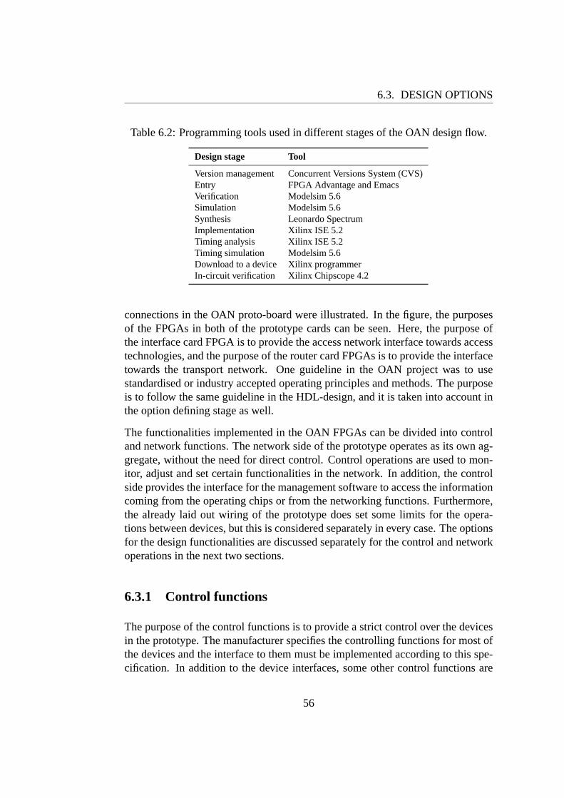
6.3. DESIGN OPTIONS
Table 6.2: Programming tools used in different stages of the OAN design flow.
Design stage Tool
Version management Concurrent Versions System (CVS)Entry FPGA Advantage and EmacsVerification Modelsim 5.6Simulation Modelsim 5.6Synthesis Leonardo SpectrumImplementation Xilinx ISE 5.2Timing analysis Xilinx ISE 5.2Timing simulation Modelsim 5.6Download to a device Xilinx programmerIn-circuit verification Xilinx Chipscope 4.2
connections in the OAN proto-board were illustrated. In the figure, the purposesof the FPGAs in both of the prototype cards can be seen. Here, the purpose ofthe interface card FPGA is to provide the access network interface towards accesstechnologies, and the purpose of the router card FPGAs is to provide the interfacetowards the transport network. One guideline in the OAN project was to usestandardised or industry accepted operating principles and methods. The purposeis to follow the same guideline in the HDL-design, and it is taken into account inthe option defining stage as well.
The functionalities implemented in the OAN FPGAs can be divided into controland network functions. The network side of the prototype operates as its own ag-gregate, without the need for direct control. Control operations are used to mon-itor, adjust and set certain functionalities in the network. In addition, the controlside provides the interface for the management software to access the informationcoming from the operating chips or from the networking functions. Furthermore,the already laid out wiring of the prototype does set some limits for the opera-tions between devices, but this is considered separately in every case. The optionsfor the design functionalities are discussed separately for the control and networkoperations in the next two sections.
6.3.1 Control functions
The purpose of the control functions is to provide a strict control over the devicesin the prototype. The manufacturer specifies the controlling functions for most ofthe devices and the interface to them must be implemented according to this spe-cification. In addition to the device interfaces, some other control functions are
56
6.3. DESIGN OPTIONS
Controlline
Controlline
PCI
LASERClocks SRAM Microp.BUS
Microp.BUS
ROUTER I/OTO CPU
Figure 6.2: The formation of the control functions in the OAN prototype.
needed in the design. Both the router and the interface card have some numberof controllable test points and LEDs to be used in the debugging and operatingstages. Furthermore, both of the cards might need some sort of a clock controllerto create and distribute different types of clocks in the design. From these assump-tions, the architecture for the functional control blocks can be derived easily andit is presented in figure 6.2. Here, the microprocessor bus interface is providedfor accessing the registers in the PMC-Sierra chips. The laser block is responsiblefor the controlling of lasers through digital-to-analogue converters and program-mable potentiometers. The PCI -block is responsible for the interface towards thePCI-bus, from where the CPU can access the whole system. Furthermore, theSRAM-chips located in the router-card have their own interfaces.
In addition to the control blocks, the control procedure needs to be determined aswell. It can be concluded quite easily, because there are no options available forthe implementation. First of all, all of the control functions need to be accessibleby the CPU, which uses the PCI-bus for the access. The operation in PCI-busis address-based as well as most of the device interface operations. The register-based access is also the only way the CPU can control these operations. So theonly solution is to make all of the functions controllable by simple register “writeand read” commands.
However, the controlling interface between different FPGAs can not be done withsimple register accesses. This is because the wiring does not allow enough con-nections between them1. For that reason, a specific control-data transport systemis needed to develop between the FPGAs. These systems must be capable fortwo-way transport and must sustain the order of the control-data. In addition,some error detection and maybe correction will be needed in the communicationchannel implemented between cards. The wiring implemented in one card can be
1For controlling operations, there are 10 signals between router and interface-cards and 4 sig-nals between the FPGAs in the router-card.
57

6.3. DESIGN OPTIONS
Tel
ecom
Bus
Tel
ecom
Bus
POSI/F
POS
PHY
3SD
HG
bEPO
S PH
Y 3
EAST RING
WEST RING
EthernetI/F
ROUTER I/O
Operations
Operations
BU
S I/
F
BU
S I/
F
Figure 6.3: The overall functionality of the OAN network.
considered error free.
6.3.2 Network functions
Networking functions are not as straightforward as control functions, but the mainfunctionalities can be identified quite easily and these are presented in figure 6.3.First of all, interfaces with PMC-Sierra device data portions need to be imple-mented in a special way, presented in the data sheets of the devices. These are theparallel TelecomBus-interfaces in the router card and POS-PHY level 3 interfacesin the interface card. The rest of the network functionality can be divided intofew specific aggregates, presented in figure 6.3. In the router card side, the DoSoperations for both of the SDH rings are performed separately and Ethernet andPOS packet processing are done in different blocks. Furthermore, the router andinterface cards need a bus interface to transport the data traffic between them, andthe same bus may also be used to transport the control traffic. The options for theimplementation of these functionalities are discussed next.
The first functional version of the OAN prototype is implemented with as lownumber of functionalities as possible, so that it could be get up and running assoon as possible. After the first version is operable, more functionalities can beadded later with little adjustments or additions in the code. In the first stage onlythe Gb Ethernet together with POS interfaces are implemented. The purpose isto transport Gb Ethernet together with POS-data over the SDH rings in the OANtest network. The Gb Ethernet will be first supported with a single HUB, whichcan be later expanded to a bridge and then to a switch. The POS line-interface isresponsible for the transport of POS-traffic between rings and the interface card.In the first stage, only the IP over SDH transport will be supported. Later thesupport can be expanded to other POS methods and to other SDH traffic as well.
58

6.3. DESIGN OPTIONS
The bus-interface between router and interface-cards needs a throughput of 10 Gbper second and for that reason it follows the PMC-Sierra specification POS-PHYLevel 4 [Inc01a]. This bus will be later expanded to support multiple cards to beconnected in the same bus.
The heart of the network operation is the DoS scheme, which is implementedfor both of the rings separately. The DoS requires the implementation of severaldifferent technologies, VC, LCAS and GFP, which all have their specific func-tionalities. Furthermore, after the DoS processing, the data must be mapped intoSDH-frames where it is transported over the OAN network. The parallel Telecom-Bus mapping requires the transported data to be mapped inside 16 SynchronousTransport Module 1 (STM-1) frame simultaneously, which is quite complicated.One solution for the ring implementation could be the all at once solution, presen-ted in figure 6.4(a). Here the transmission side (TX) operates in the followingway: the transmitted data comes from the Ethernet or POS interfaces and goesfirst into GFP-framer. The Ethernet and POS data are processed separately andhanded further for the VC-processor, which classifies them into Virtual Concaten-ation Groups (VCGs). In the figure, the TDM-data means the telephone networktraffic and it will be implemented in a later stage of the network development.After the data is assorted according to the destination and QoS or LCAS require-ments, the creation of STM-1 frames can begin. SDH containers, created in thevirtual concatenation stage, are mapped inside the STM-1 frames, which are thenfurther mapped into the TelecomBus. These procedures are presented in more de-tail in [IT00c][IT00a][Inc01c] and discussed in the next chapter. Furthermore, theAPS is responsible for forwarding of traffic towards the operating ring if there isa failure in the other ring.
However, the formation of the configuration memory is needed to consider. Wecould create all of the 16 STM-1 frames first in the memory and only after thatmap them into TelecomBus. The STM-1 consist of bytes in 9 rows and 270columns, requiring a minimum of16 × 9 × 270B = 38880B = 311040b ofmemory for a single SDH transport operation. In addition, another memory spacewould be needed for the creation of the second 16 STM-1 frames, while the firstones are mapped into TelecomBus. The amount of memory required here exceedsthe available fast RAM memories inside the FPGA chips and does not seem soefficient in other ways either. It seems that restoring of the data is needed to do inthe virtual concatenation stage, where different sizes of containers could be cre-ated for the STM-1 frames. The mapping of STM-1 frames into TelecomBus canthen be done simultaneously as the creation of the frames. However, the imple-mentation of the VCG-memories needs to be considered separately.
The all at once principle presented in figure 6.4(a) gives an idea of the operation,
59
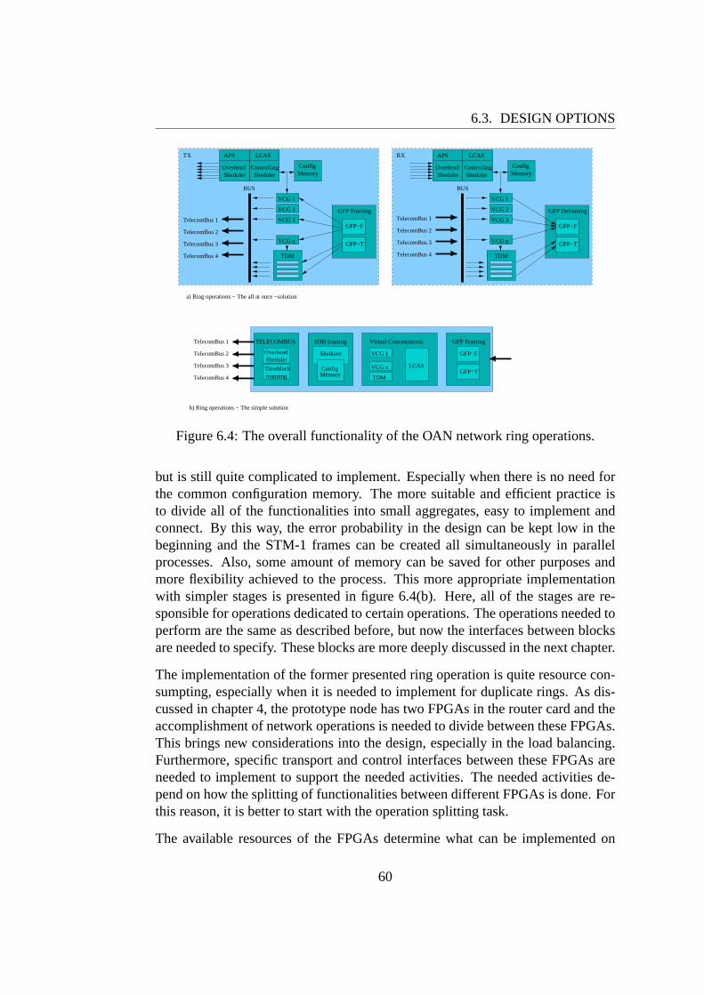
6.3. DESIGN OPTIONS
BUS
TX
VCG n
VCG 3
VCG 2
VCG 1
APS
Overhead
LCAS
ShedulerControlling
Sheduler
TDM
SDH framingTELECOMBUS
OverheadSheduler
ConfigMemory
Sheduler
mappingTimeblock
b) Ring operations − The simple solution
a) Ring operations − The all at once −solution
GFP−F
GFP−T
GFP Framing
VCG n
TDM
VCG 1
Virtual Concatenation
LCAS
TelecomBus 2
TelecomBus 3
TelecomBus 4
TelecomBus 1
TelecomBus 2
TelecomBus 3
TelecomBus 4
TelecomBus 1GFP−F
GFP−T
GFP Framing
RX
VCG 1
VCG 2
VCG 3
VCG n
BUS
APS
Overhead
LCAS
ShedulerControlling
Sheduler
ConfigMemory
TDM
TelecomBus 2
TelecomBus 3
TelecomBus 4
TelecomBus 1GFP−F
GFP−T
GFP Deframing
ConfigMemory
Figure 6.4: The overall functionality of the OAN network ring operations.
but is still quite complicated to implement. Especially when there is no need forthe common configuration memory. The more suitable and efficient practice isto divide all of the functionalities into small aggregates, easy to implement andconnect. By this way, the error probability in the design can be kept low in thebeginning and the STM-1 frames can be created all simultaneously in parallelprocesses. Also, some amount of memory can be saved for other purposes andmore flexibility achieved to the process. This more appropriate implementationwith simpler stages is presented in figure 6.4(b). Here, all of the stages are re-sponsible for operations dedicated to certain operations. The operations needed toperform are the same as described before, but now the interfaces between blocksare needed to specify. These blocks are more deeply discussed in the next chapter.
The implementation of the former presented ring operation is quite resource con-sumpting, especially when it is needed to implement for duplicate rings. As dis-cussed in chapter 4, the prototype node has two FPGAs in the router card and theaccomplishment of network operations is needed to divide between these FPGAs.This brings new considerations into the design, especially in the load balancing.Furthermore, specific transport and control interfaces between these FPGAs areneeded to implement to support the needed activities. The needed activities de-pend on how the splitting of functionalities between different FPGAs is done. Forthis reason, it is better to start with the operation splitting task.
The available resources of the FPGAs determine what can be implemented on
60

6.3. DESIGN OPTIONS
each of the devices. First of all, we can calculate the requirements for the memoryused in VCGs in the first stage of the OAN prototype implementation. If there is16 of them in one direction, it takes together4 × 16 = 64 VCGs in the design.One VCG will use one Select RAM memory primitive at a minimum and there-fore the amount of Select RAM memory primitive available2 in the smaller FPGAin the router card is not enough. So we need to split the ring operations betweenthese two FPGAs. There are only two potential ways to split the ring operations.One is between the GFP and the virtual concatenation blocks, and the other isbetween SDH framing and TelecomBus mapping blocks. The third potential split-ting between SDH framing and virtual concatenation blocks can be consideredimpossible, because of the number of connections needed between them. Further-more, the TelecomBus mapping requires access to the SDH framing configurationinformation, which cannot be efficiently moved with the data. It seems that thesplitting is needed to be done after the parallel TelecomBus mapping and the datawith the overhead is needed to transport to the smaller FPGA for direct connectioninto the physical TelecomBus interface.
In this situation, the only way to avoid the need for transport protocol would beconnecting the TelecomBus signals directly from the physical TelecomBus in-terface in the smaller FPGA to the larger FPGA. However, this is not possiblebecause the two parallel TelecomBus interfaces requires together 248 signals andonly 184 connections are implemented between the FPGAs in the router card. Soa specific transport system is needed to develop between the FPGAs. The imple-mentation of this transport protocol or system is more deeply discussed in the nextchapter.
The physical network structure in the OAN prototype takes care of the networkprotection, as discussed in chapter 4. For this reason, the implementation of APSin the HDL design is not necessary, but it will be included in the design for futurepurposes. This is because the OAN is a metropolitan area test network and atthe moment it seems that the protection and survivability features in this areawill be even more important in the future than they have been before. Becauseof the small utilisation of the smaller FPGA, it would be nice to have at leastthe APS implemented there. However, APS requires information available in theSDH frames and it is needed to locate next to the SDH framing and deframingprocedures.
2XC2V2000-FF896 has 56 Select RAM primitives as presented in table 6.1.
61

Chapter 7
HDL Design
Based on the discussions in the previous chapter, the design for the HDL imple-mentation of the OAN prototype FPGAs is presented in this chapter. The present-ation follows the structure of the design specification model, presented in chapter5. Only the detailed technical definitions of the functionalities are left out to keepthe number of the pages of this thesis in decent limits. The details presented herecover the main functionality of the design and interfaces between different blocks.Most of the functionalities are based on the results of the previous development inthe industry and more accurate information can be found from the source literat-ure. The reason why there is so much source information available is the originalOAN suggestion that as much of the functionalities as possible should be basedon standards. This is the truth only for part of the functionalities, but nearly allof the rest are based on industry recommendations or specifications. Furthermore,part of the design is a result of own development and these functionalities arepresented with adequate details. This issue is further discussed in the followingsection.
7.1 Design functionality
The options for the implementation were discussed in the previous chapter andbased on these assumptions, the overall design architecture is presented in figure7.1. The network and control operations are separated from each other, becausecontrolling of the network operations happens only with non-direct settings. Thenetwork side has two SDH-interfaces, west and east rings. Their operations areidentical to each other, and the APS block is connected to both of them. The ring
62
7.2. DISTRIBUTION OF CLOCKS
operations are responsible for the building of the SDH payload and frame. ThePOS and GbE packet scheduler blocks direct the network packets into right dir-ections, which are either towards one of the rings or towards the interface card.The POS-PHY level 4 interface is responsible for the transportation of data pack-ets between router and interface cards and the POS-PHY level 3 interface is usedfor data packet arbitration between PMC-Sierra devices in the interface card. TheFIFO controller handles the buffering of packets between POS-PHY interfaces.The I/O control is responsible for the controlling operations in the interface card.Otherwise the control side of the implementation is the same as presented in theprevious chapter.
From the design blocks presented in figure 7.1, the functionality of TelecomBus,POS-PHY Level 3, POS-PHY Level 4, SRAM, PCI and microprocessor bus in-terfaces is provided directly by a set of industry specifications or device data-sheets, to be presented later. The only thing left for designing, is the functionalityand composition of the interface towards the other operations inside the FPGAs.Furthermore, all of the networking functionalities1 are based on standards. Thedesigning task here is to clarify how these standards can be supported by hard-ware solutions, because the standards specify only the needed operations, not theimplementation. The rest of the design blocks need to be created purely by thedesigner. Here, one important part of the planning is defining the interfaces andoperations between different blocks. In figures 7.2 and 7.3 the signals betweendifferent blocks in the FPGAs are presented together with more detailed designstructures.
The larger FPGA in the router card is illustrated in figure 7.2, the smaller FPGAin the router card in figure 7.3(a) and the interface card FPGA in figure 7.3(b).These figures give some understanding on the operating principles of each of theinterfaces. However, a more accurate description will be given later in the thesis,together with a detailed presentation of the functionalities of the design blocks.Furthermore, the interfaces between FPGAs are also discussed later.
7.2 Distribution of clocks
One important part of the network design is the clocking scheme. The SDH tech-nology has specific requirements for the source clocks and clock synchronisation,which both need to be considered. The OAN prototype has a variety of differ-ent clock sources, illustrated in figure 7.4. First of all, the two oscillators loc-
1SDH, VC, LCAS, GFP, GbE and POS.
63

7.2. DISTRIBUTION OF CLOCKS
Clock
controlL
ASE
RSR
AM
Microp.
BU
SP
CI
RO
UT
ER
control
Control
lineC
ontrolline
I/Ocontrol
Microp.
BU
S
XC
2V6000−
FF1152
XC
2V1000−
FF896
Incoming
Outgoing
Incoming
WE
ST R
ING
XC
2V2000−F
F896
Outgoing
EA
ST R
ING
Defram
ing
SDH
SDH
Fram
ing
SDH
Defram
ing
SDH
Fram
ing
VC
LC
AS
LC
AS
VC
GF
P
Fram
ing
Defram
ing
GF
P
GF
P
Fram
ing
GF
P
Defram
ingL
CA
S
VC
LC
AS
VC
GbE
packetscheduler
PO
Spacket
scheduler
FIF
O
GbE Interface SDH Interface
INTERFACE
INTERFACE
INPUTINPUT
INPUT INPUT
INTERFACEINTERFACESerial TelecomBus Serial TelecomBus
Telecom
Bus m
apping
Telecom
Bus m
apping
Pre−TBusPre−TBusPre−TBusPre−TBusOUTPUT OUTPUT
OUTPUTPre−TBusPre−TBusPre−TBus
OUTPUTPre−TBus
POS−PHY Level 4
POS−PHY Level 4
Controller
POS−PHY Level 3POS−PHY Level 3
AP
S
Figure 7.1: The functionality of the FPGAs in the OAN prototype.
64
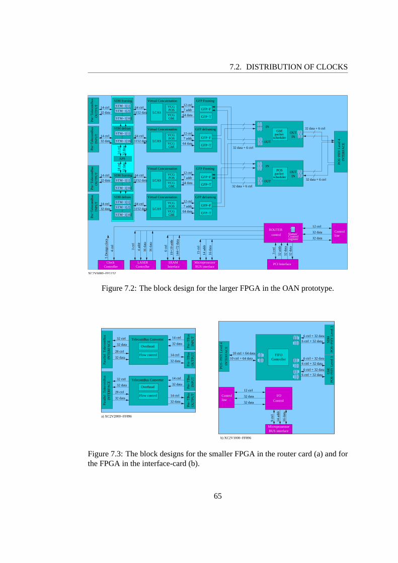
7.2. DISTRIBUTION OF CLOCKS
POSpacket
scheduler
VCG
32 d
ata
32 d
ata
32 a
ddr
3 ct
rl
32 data + 6 ctrl
32 data + 6 ctrl
32 data + 6 ctrl
32 data + 6 ctrl
32 data
32 data
12 ctrl
16 d
ata
14 a
ddr
15 c
trl
19+
19 a
ddr
144+
72 d
ata
6 ct
rl
GbE
POS
GbE
POS
64 data
12 ctrl
12 ctrl
64 data
GbE
POS
GbE
POS
64 data
12 ctrl
12 ctrl
64 data
STM−1[16]
STM−1[1]
STM−1[1]
STM−1[16]
APS
5 D
esig
n cl
ocs
4 ct
rl
3 ct
rl
4 ad
dr
16 d
ata
16 d
ata
7 addr
7 addr
7 addr
7 addr
64 ctrl
1152 data
64 ctrl
1152 data
64 ctrl
1152 data
64 ctrl
1152 data
STM−1[16]
STM−1[2]
STM−1[1]
STM−1[16]
STM−1[2]
STM−1[1]
14 ctrl
14 ctrl
14 ctrl
14 ctrl
14 c
trl
14 c
trl
32 d
ata
32 d
ata
32 data
32 data
32 data
32 data
ControllerClock
ControllerLASER SRAM
InterfaceMicroprosessorBUS interface
ROUTER
control
PCI Interface
Controlregister
Status/Controlline
POS−
PHY
Lev
el 4
INT
ER
FAC
E
XC2V6000−FF1152
Virtual Concatenation
LCAS
Virtual Concatenation
LCAS
SDH defram
VCG
VCG
VCG
Virtual Concatenation
LCAS
Virtual Concatenation
LCASVCG
VCG
VCG
SDH framing
Pre−
Tel
ecom
Bus
Pre−
Tel
ecom
Bus
INPU
TO
UT
PUT
Pre−
Tel
ecom
Bus
Pre−
Tel
ecom
Bus
INPU
TO
UT
PUT
SDH framing
SDH defram
INOUT
OUT
IN
packetscheduler
GbE
INOUT
OUT
IN
GFP−F
GFP−T
GFP deframing
GFP Framing
GFP−F
GFP−T
GFP−F
GFP−T
GFP deframing
GFP Framing
GFP−F
GFP−TVCG
Figure 7.2: The block design for the larger FPGA in the OAN prototype.
6 ctrl + 32 data
6 ctrl + 32 data
6 ctrl + 32 data
6 ctrl + 32 data
6 ctrl + 32 data
6 ctrl + 32 data
10 ctrl + 64 data
10 ctrl + 64 data
32 data
32 data
12 ctrl
14 a
ddr
16 d
ata
9 ct
rl
Flow control
32 data
14 ctrl
28 ctrl
32 data
32 ctrl
32 data
32 data
14 ctrl
Flow control
32 data
14 ctrl
32 data
14 ctrl28 ctrl
32 data
32 ctrl
32 data
Controlline
I/O
Control
MicroprosessorBUS interface
a) XC2V2000−FF896
ControllerFIFO
b) XC2V1000−FF896
Para
llel
Tel
ecom
Bus
INT
ER
FAC
E
TelecomBus Converter
Overhead Pre−
TB
usIN
PUT
Pre−
TB
usO
UT
PUT
Para
llel
Tel
ecom
Bus
INT
ER
FAC
E
TelecomBus Converter
Overhead Pre−
TB
usIN
PUT
Pre−
TB
usO
UT
PUT
POS−
PHY
Lev
el 4
INT
ER
FAC
E
POS−
PHY
Lev
el 3
SDH
POS−
PHY
Lev
el 3
GbE
Figure 7.3: The block designs for the smaller FPGA in the router card (a) and forthe FPGA in the interface-card (b).
65
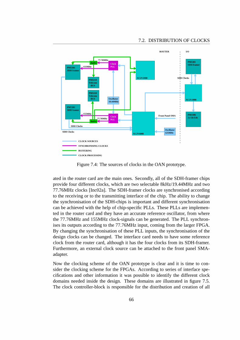
7.2. DISTRIBUTION OF CLOCKS
SDH Clocks
CLOCK SOURCES
SYNCHRONISING CLOCKS
BUFFERING
77.76MHz
155MHz
155MHz
77.76MHz
Front Panel SMA
SDH Clocks
SDH Clocks
CLOCK PROCESSING
XC2V6000
Buffer
Buffer
PM5310Telecom
PM5310Telecom
Oscillator125MHz
Oscillator19.44MHz
ClockPLL
ClockPLL
BUS
BUS
PM5381SDH framer
PM5381SDH framer
XC2V2000
XC2V1000
ROUTER
PM33862x Gb Eth
SDH framerPM5381
I/O
Figure 7.4: The sources of clocks in the OAN prototype.
ated in the router card are the main ones. Secondly, all of the SDH-framer chipsprovide four different clocks, which are two selectable 8kHz/19.44MHz and two77.76MHz clocks [Inc02a]. The SDH-framer clocks are synchronised accordingto the receiving or to the transmitting interface of the chip. The ability to changethe synchronisation of the SDH-chips is important and different synchronisationcan be achieved with the help of chip-specific PLLs. These PLLs are implemen-ted in the router card and they have an accurate reference oscillator, from wherethe 77.76MHz and 155MHz clock-signals can be generated. The PLL synchron-ises its outputs according to the 77.76MHz input, coming from the larger FPGA.By changing the synchronisation of these PLL inputs, the synchronisation of thedesign clocks can be changed. The interface card needs to have some referenceclock from the router card, although it has the four clocks from its SDH-framer.Furthermore, an external clock source can be attached to the front panel SMA-adapter.
Now the clocking scheme of the OAN prototype is clear and it is time to con-sider the clocking scheme for the FPGAs. According to series of interface spe-cifications and other information it was possible to identify the different clockdomains needed inside the design. These domains are illustrated in figure 7.5.The clock controller-block is responsible for the distribution and creation of all
66

7.3. CONTROL PART
the clocks in the design. The selection options for each of the clock frequenciesare further discussed in the specification part of the clock controller or the otherblocks respectively. All of the different clock domains are separated with specialFIFO architecture, which have two ports, both operating with different frequen-cies. Without this kind of clock separating, different clock domains would be hardto implement in the design.
7.3 Control part
As it was stated earlier, the control part is responsible for the adjustment, settingand monitoring functions of the network part. Together with these, it has controlinterfaces towards all of the devices in the prototype, and it controls the LEDsand test points in the design. Of course, one important feature in the controlpart is the modification and distribution of the clocks in the design. Furthermore,the CPU needs to have access to read and write registers in all of the controllabledevices. In addition, some amount of controlling ability is needed for the functionsinside the FPGAs as well. For the controlling operations, every device has acertain number of registers, which can be read or written. In addition, the designcontrol procedures require some number of registers to be created into the design.These registers are located in the router control block, and they are named as theStatus/Control-registers and further discussed in the following.
7.3.1 Registers
All of the devices in the prototype can be controlled through a simple register“read and write” commands. For this purpose, all of the devices have a certainnumber of registers need to be accessed by the CPU. The address spaces for eachof the devices is presented in table 7.1. The registers in the devices are only 16-bit wide and the 32-bit wide PCI-bus cannot access all of them. For that reason,simple address conversion is needed between the PCI-bus and the registers in theprototype. The mapping of each of the devices PCI-addresses is presented intable 7.2. In addition to the devices in the router card, the interface card has itsown devices. However, these devices cannot be accessed in the same way as thedevices in the router card and are left out from the PCI-addressing. The accessingof these devices is discussed in the next section.
The control functionalities need to be implemented inside the FPGAs are mappedinto register read and write procedures in the Status/Control register. With re-
67
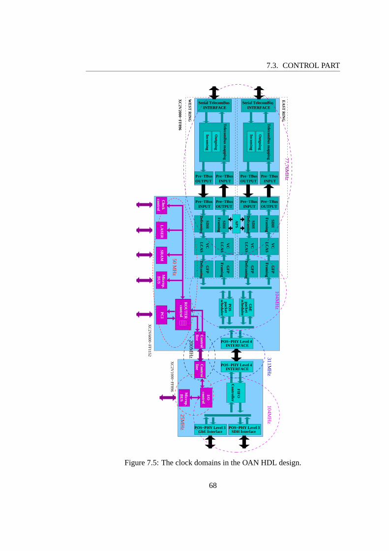
7.3. CONTROL PART
Clock
controlL
ASE
RSR
AM
Microp.
BU
SP
CI
RO
UT
ER
control
Control
lineC
ontrolline
I/Ocontrol
Microp.
BU
S
XC
2V6000−
FF1152
XC
2V1000−
FF896
Incoming
Outgoing
Incoming
WE
ST R
ING
XC
2V2000−F
F896
Outgoing
EA
ST R
ING
Defram
ing
SDH
SDH
Fram
ing
SDH
Defram
ing
SDH
Fram
ing
VC
LC
AS
LC
AS
VC
GF
P
Fram
ing
Defram
ing
GF
P
GF
P
Fram
ing
GF
P
Defram
ingL
CA
S
VC
LC
AS
VC
GbE
packetscheduler
PO
Spacket
scheduler
FIF
O
GbE Interface SDH Interface
INTERFACE
INTERFACE
INPUTINPUT
INPUT INPUT
INTERFACEINTERFACESerial TelecomBus Serial TelecomBus
Telecom
Bus m
apping
Telecom
Bus m
apping
Pre−TBusPre−TBusPre−TBusPre−TBusOUTPUT OUTPUT
OUTPUTPre−TBusPre−TBusPre−TBus
OUTPUTPre−TBus
POS−PHY Level 4
POS−PHY Level 4
Controller
POS−PHY Level 3POS−PHY Level 3
AP
S
104MH
z
25MH
z
50 MH
z
77,76MH
z
311MH
z
104MH
z
200MH
z
Figure 7.5: The clock domains in the OAN HDL design.
68
7.3. CONTROL PART
Table 7.1: The device address spaces in the OAN prototype.
Address space Width Chip
720H 11 PM3386 (Gbit Ethernet)502H 12 PM5310 (TelecomBus serializer/deserializer)890H 14 PM5381 (SONET/SDH framer/deframer)
Table 7.2: The address mappings in the Router control block.
Node address PCI Address Type Board Circuit/block
00000 - 00FFF 00000 - 01FFF R/W Node Status/Control register01000 - 01FFF 02000 - 03FFF R/W Node S/UNI-2488 ring A (PM5381)02000 - 02FFF 04000 - 05FFF R/W Node S/UNI-2488 ring B (PM5381)03000 - 03FFF 06000 - 07FFF R/W Node PM5310 A04000 - 04FFF 08000 - 09FFF R/W Node PM5310 B
gister structure, the needed functionalities can be arranged and a specific addressprovided with each of them. The Status/Control register in the OAN prototypeis used to give commands to different instances in the design. It can also beused for monitoring purposes, for example error monitoring or network statist-ics. Furthermore, in this case the access to the interface card is implementedthrough Status/Control-register. The address spaces in the Status/Control registeris presented in table 7.3 and in each space, sufficient number of registers is definedfor the potentially needed functionalities. All of the registers are 16-bits wide andthey can be accessed with 32-bit address.
7.3.2 Accessing the interface card registers
The registers located in the interface card cannot be accessed similarly as theregisters in the router card. The reason for this is the slow control connectionbetween router and interface cards. The connection has a small number of sig-nals, and the data must be transported in serial form. With the clock frequenciesavailable for the purpose, the connection cannot be fast enough for the PCI-access.For that reason, another way or system is needed for the communication betweenthe interface card and the CPU. This implementation block, named control line, ispresented in detail later on in this chapter, but the procedure needed to access theregisters in the interface card is illustrated here. The registers in the interface cardare also 16-bit wide and to address all of them, a 15-bit wide address is needed.
69
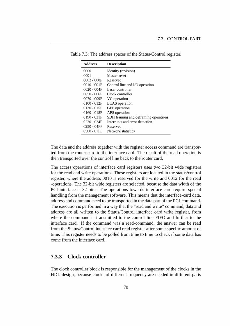
7.3. CONTROL PART
Table 7.3: The address spaces of the Status/Control register.
Address Description
0000 Identity (revision)0001 Master reset0002 - 000F Reserved0010 - 001F Control line and I/O operation0020 - 004F Laser controller0050 - 006F Clock controller0070 - 009F VC operation0100 - 012F LCAS operation0130 - 015F GFP operation0160 - 018F APS operation0190 - 021F SDH framing and deframing operations0220 - 024F Interrupts and error detection0250 - 04FF Reserved0500 - 07FF Network statistics
The data and the address together with the register access command are transpor-ted from the router card to the interface card. The result of the read operation isthen transported over the control line back to the router card.
The access operations of interface card registers uses two 32-bit wide registersfor the read and write operations. These registers are located in the status/controlregister, where the address 0010 is reserved for the write and 0012 for the read-operations. The 32-bit wide registers are selected, because the data width of thePCI-interface is 32 bits. The operations towards interface-card require specialhandling from the management software. This means that the interface-card data,address and command need to be transported in the data part of the PCI-command.The execution is performed in a way that the “read and write” command, data andaddress are all written to the Status/Control interface card write register, fromwhere the command is transmitted to the control line FIFO and further to theinterface card. If the command was a read-command, the answer can be readfrom the Status/Control interface card read register after some specific amount oftime. This register needs to be polled from time to time to check if some data hascome from the interface card.
7.3.3 Clock controller
The clock controller block is responsible for the management of the clocks in theHDL design, because clocks of different frequency are needed in different parts
70
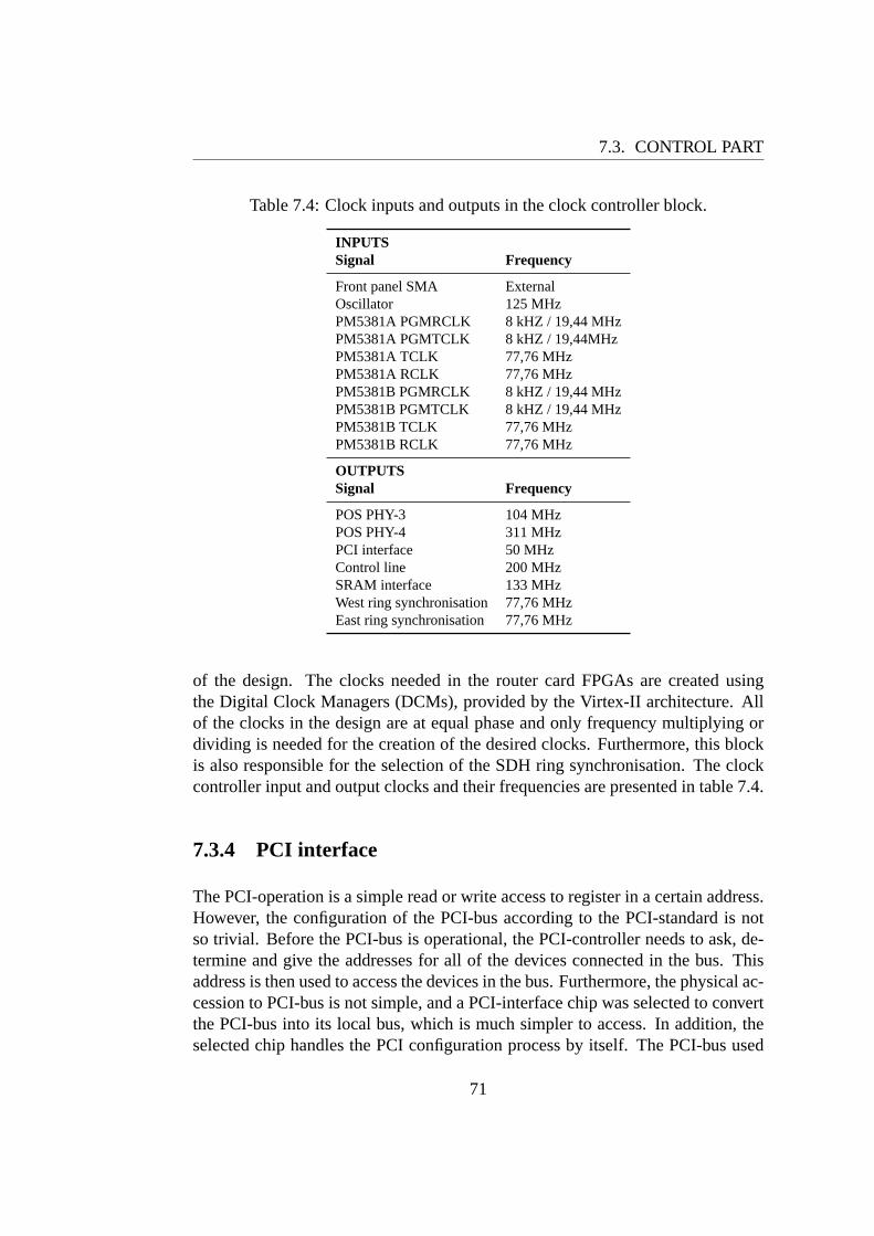
7.3. CONTROL PART
Table 7.4: Clock inputs and outputs in the clock controller block.
INPUTSSignal Frequency
Front panel SMA ExternalOscillator 125 MHzPM5381A PGMRCLK 8 kHZ / 19,44 MHzPM5381A PGMTCLK 8 kHZ / 19,44MHzPM5381A TCLK 77,76 MHzPM5381A RCLK 77,76 MHzPM5381B PGMRCLK 8 kHZ / 19,44 MHzPM5381B PGMTCLK 8 kHZ / 19,44 MHzPM5381B TCLK 77,76 MHzPM5381B RCLK 77,76 MHz
OUTPUTSSignal Frequency
POS PHY-3 104 MHzPOS PHY-4 311 MHzPCI interface 50 MHzControl line 200 MHzSRAM interface 133 MHzWest ring synchronisation 77,76 MHzEast ring synchronisation 77,76 MHz
of the design. The clocks needed in the router card FPGAs are created usingthe Digital Clock Managers (DCMs), provided by the Virtex-II architecture. Allof the clocks in the design are at equal phase and only frequency multiplying ordividing is needed for the creation of the desired clocks. Furthermore, this blockis also responsible for the selection of the SDH ring synchronisation. The clockcontroller input and output clocks and their frequencies are presented in table 7.4.
7.3.4 PCI interface
The PCI-operation is a simple read or write access to register in a certain address.However, the configuration of the PCI-bus according to the PCI-standard is notso trivial. Before the PCI-bus is operational, the PCI-controller needs to ask, de-termine and give the addresses for all of the devices connected in the bus. Thisaddress is then used to access the devices in the bus. Furthermore, the physical ac-cession to PCI-bus is not simple, and a PCI-interface chip was selected to convertthe PCI-bus into its local bus, which is much simpler to access. In addition, theselected chip handles the PCI configuration process by itself. The PCI-bus used
71
7.3. CONTROL PART
in OAN has 32-bit wide address and 32-bit wide data. Most of the registers in theOAN prototype have 16-bit wide data and the less significant part of the PCI-databus is used for them. In PCI-operation, the command is first written to the device,specified by the address, and the bus is halted as long as the ready-indication isreceived from the device. The PCI write-operation is thus quick, but the durationof the read operation depends on the target device. This is the reason, why theinterface card register access was implemented in a special way.
The PCI-interface is implemented with the help of PCI9030-chip, which convertsthe PCI-bus into its local bus [Tec00]. The local bus is configurable and allows theuse of clock frequency between 33-66 MHz and most importantly, multiplexingof address and data over the same bus. With multiplexing some of the input outputpins in the FPGA can be saved for other use. The selected chip is widely used inthe industry and it should function properly. Furthermore, the PCI standard hasstrict limits for the physical connection lengths between the PCI adapter and thePCI chip. For that reason, connecting the PCI bus directly to the prototype FPGAwould have been too complicated and it was left out from the design.
The purpose of the PCI-interface block is to provide the interface to the PCI9030local bus. The interface has two operations, read and write. The address and datafor the read and write operations are multiplexed from the local bus and need tobe changed into parallel form for the operations in the FPGA. The interface tothe local bus is described with detail in [Tec00]. Furthermore, the interface to therouter control has separated address and separated read and write data lines. It hasa signal that indicates the start of operation and a signal that is asserted when theoperation is ready. The operating clock for the local bus and for the interface isselected to be 50 MHz.
7.3.5 Router control
The router control block is the core of the control operations, and every com-mand is transported through it. Its main operation is the address mapping betweendevices and control functions. Several devices can be attached to this micropro-cessor bus, but only one device can be accessed at a certain time. The accesseddevice is indicated with a chip-select signal and one purpose of the router controlis to change the PCI-addresses into these chip-select signal assertions. Further-more, the router control is responsible for converting the Status/Control registerread and write operations into control functions in the design. The address map-ping for each of the devices were presented in table 7.2 and the structure of theStatus/Control register in table 7.3.
72
7.3. CONTROL PART
The router control block interfaces with all of the other control blocks in the routercard. These interfaces were presented in figure 7.2 and more deeply covered in thespecification of the respective blocks. Controlling of eight LEDs and several testpoints are one of the responsibilities of the router control. Furthermore, after thefirst version of the OAN network is operational, the router control block will be theblock where automatic error detection systems and interrupt handling operationsare to be implemented.
7.3.6 I/O control
Like the router control in the router card, the I/O control is an interface for the con-trol operations in the interface card. The interface card has less controlling opera-tions than the router card, and all needed ones are implemented in the I/O controlblock. In the first stage, there is no need to build a separate register structure in theinterface card, because only the access to the device registers is needed. Further-more, the clock control is implemented according to the specifications plannedbeforehand, and there is no need for the ability to change synchronisation. Thechip-selects signals need to be controlled by the I/O control, like the eight LEDsand test points in the interface card. In the later versions of the design, the in-terrupt handling and some automatic monitoring can be implemented in the I/Ocontrol.
7.3.7 Control line
The control line is a simple one-bit parallel line interface with Cyclic RedundancyCheck (CRC) error checking. It has a two-way transport for 36-bit wide dataover three signals per transport direction. In addition to data transport, the blockcalculates a 4-bit wide CRC-checksum for the transported data in the transferside and verifies it in the receiver side. If the checksum does not match, thetransported data is ignored. The calculated CRC-checksum is polynomial andof form X4 + X + 1. It will be calculated using the hardware implementationillustrated in figure 7.6.
The data to be transported is given to control line through a simple FIFO-interface.The 36-bit wide FIFO is located in the control line block and the 36-bit wide datasequences are transported in the order of their arrival. The FIFO interface consistsof 36-bit data and full and write enable signals. The receive data interface issimilar and consist of 36-bit data, empty and read enable signals. The controlline blocks have FIFO interfaces with both router control and I/O control blocks.
73
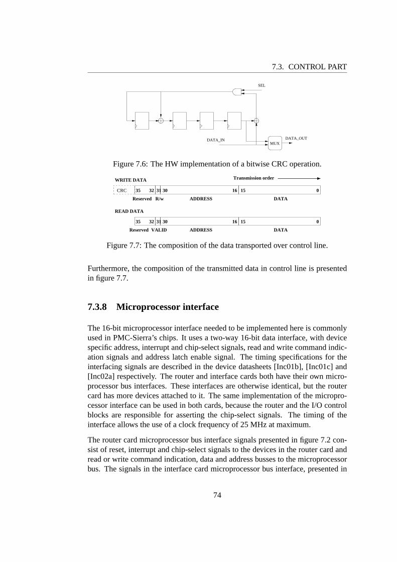
7.3. CONTROL PART
MUXDATA_OUT
SEL
DATA_IN
Figure 7.6: The HW implementation of a bitwise CRC operation.
35 32 31 30 16 15 0
DATAADDRESS
Transmission order
VALID
CRC
WRITE DATA
READ DATA
35 32 31 30 16 15 0
DATAADDRESSR/wReserved
Reserved
Figure 7.7: The composition of the data transported over control line.
Furthermore, the composition of the transmitted data in control line is presentedin figure 7.7.
7.3.8 Microprocessor interface
The 16-bit microprocessor interface needed to be implemented here is commonlyused in PMC-Sierra’s chips. It uses a two-way 16-bit data interface, with devicespecific address, interrupt and chip-select signals, read and write command indic-ation signals and address latch enable signal. The timing specifications for theinterfacing signals are described in the device datasheets [Inc01b], [Inc01c] and[Inc02a] respectively. The router and interface cards both have their own micro-processor bus interfaces. These interfaces are otherwise identical, but the routercard has more devices attached to it. The same implementation of the micropro-cessor interface can be used in both cards, because the router and the I/O controlblocks are responsible for asserting the chip-select signals. The timing of theinterface allows the use of a clock frequency of 25 MHz at maximum.
The router card microprocessor bus interface signals presented in figure 7.2 con-sist of reset, interrupt and chip-select signals to the devices in the router card andread or write command indication, data and address busses to the microprocessorbus. The signals in the interface card microprocessor bus interface, presented in
74

7.3. CONTROL PART
figure 7.3(b) are the same as in the router card, although the interface card hasless devices attached than the router card and so less signals are needed in thatinterface.
7.3.9 SRAM interface
The router card has six512k× 36 SRAM chips, which all have 2 MB of memory,providing together 12 MB of memory to be used in the operations in the routercard. This memory is attached in the router card for the routing calculation pur-poses and is therefore not used in the first stage of the design implementation.However, the connections to the memory chips need to be tested and access to thememory is needed for that reason. The SRAM interface block provides access tothe memory space. The six memory chips are connected with the larger FPGA,forming two larger memory blocks. One block is 144 bits wide and the otherblock is 36 bits wide, and they both have 19-bit address buses. The memoriessupport single and burst read and write operations. The interface timing specifica-tion of the memory chips are presented in their datasheet [Ele01]. The connectionsbetween the router control and the SRAM interface block consist of separate dataand address busses for each of the memory blocks together with three control sig-nals for each of them. These control signals indicate the operation (read or write),the start of operation and the operation ready indication. The SRAM blocks op-erate at most at a frequency of 133 MHz, which is selected for their operatingpurposes.
7.3.10 Laser controller
The router card has two optical tranceivers2, which can transmit with a wavelengthof 1550 nm and receive wavelengths between 1300-1550 nm. The receivers areused in the SDH transport network, but the transmitters are used only for test pur-poses. In addition to the transceivers, the router card has two tuneable transmitters,controllable through the Status/Control register. These tuneable transmitters areused in the OAN transport network and can be disabled if needed. The laser con-troller block is responsible for the controlling of the tuneable laser modulation andbias currents together with their temperatures (wavelength). It is also responsiblefor the temperature monitoring of all of the lasers included in OAN. It has optionaleight temperature monitoring interfaces for pump lasers used in optical amplifiers.These interfaces can be used for monitoring the network amplifiers.
2Transceiver is a device, which has both the transmitter and receiver implemented in it.
75
7.3. CONTROL PART
The laser settings on the card are analogue in their nature and for that reasonanalogue to digital converters are used when monitoring values from the lasers.In addition, digital potentiometers and digital to analogue converters are usedwhen controlling the lasers. Here, following equipment are used: 12-bit ADCMAX1247 [Pro01], 12-bit DAC MAX531, [Pro97], single digitally controlled po-tentiometer (X9110) [Inc00a] and dual digitally controlled potentiometer (X9221)[Inc00b]. The monitoring and controlling operations are accessed through theStatus/Control-register.
Control operations
These controlling tasks can be done for both tuneable lasers separately. Both mod-ulation and pre-bias currents can be controlled manually or automatically. Assert-ing the right jumper in the router card will make the selection. In addition, both ofthe automatic and manual controllers can be accessed through the Status/Controlregister. Furthermore, all of the equipment mentioned here have a specific opera-tion sequence, which can be found from each of their datasheets respectively. Thevalues needed in these operations are preserved in the Status/Control register. Thefollowing list presents the laser controlling operations.
• Set tuneable laser temperature (wavelength)— Both tuneable lasers havetheir own controllers, which use the MAX531 digital to analogue converter.This converter has a specific operation sequence, which can be found fromthe MAX531 datasheet [Pro97].
• Set tuneable laser pre-bias current— Manual pre-bias current control isdone with the help of a single digitally controlled potentiometer (X9110)[Inc00a] and automatic pre-bias current controlling with the help of dualdigitally controlled potentiometer (X9221) [Inc00b].
• Set tuneable laser modulation current— Manual modulation currentcontrol is done with the help of a single digitally controlled potentiometer(X9110) [Inc00a] and automatic modulation current controlling with thehelp of dual digitally controlled potentiometer (X9221) [Inc00b].
Monitor operations
Laser monitoring operations use the Status/Control register as their control inter-face as well. The value of a monitored function can be checked by first asserting
76

7.4. NETWORK PART
the command into the register and after some while reading the result from otherregister. Nevertheless, a more desired option is to monitor the values continu-ously. The continuous monitoring asserts a new command for the analogue todigital converters over and over again and updates the result register after eachoperation. By this way, the most recent information is always available in theStatus/Control register. This allows the implementation of an automatic monitor-ing system, where the monitored values are compared to some threshold value. Ifthe threshold value is exceeded, an error condition exists. Automatic monitoringsystems are implemented in the later stage of the design and not considered here.The following list presents the laser monitoring operations.
• Monitor laser temperature — Temperature monitoring can be done for allof the four lasers with a single four-channel MAX1247, which is implemen-ted in the router card for that purpose. This converter has a specific opera-tion sequence, which can be found from the MAX1247 datasheet [Pro01].
• Monitor transceiver bias — The bias currents of the transceivers can bemonitored with a single signal, which indicates the end of life or laser OKconditions.
• Monitor pump laser temperature — The router card has an interface im-plemented, which allows the monitoring of 8 separate pump lasers temper-ature. Two MAX1247 is used for the interfacing purpose.
7.4 Network part
The network part of the design is responsible for all of the networking functionsimplemented in the design. This covers both the transport network functions andthe access network functions. The transport network interface and functionality isimplemented in the router card and the access network interface and functional-ity in the interface card. To transfer data between these interfaces, a special datatransporting functionality needs to be implemented. The purpose of the trans-port network side is to implement the DoS functionality, and the purpose of theinterface side is to make the access technology conversions.
7.4.1 POS-PHY level 3
The POS-PHY level 3 is an interface for the interconnection of Physical Layer(PHY) devices to Link Layer devices, recommended by PMC-Sierra. It provides
77
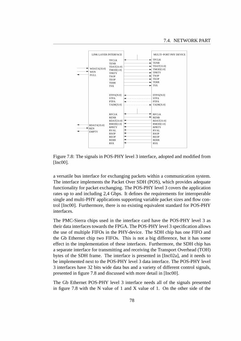
7.4. NETWORK PART
RFCLKRENBRDAT[31:0]RMOD[1:0]RPRTYRVALRSOPREOPRERRRSX
STPAPTPA
DTPA[N:0]
TADR[X:0]
TFCLKTENBTDAT[31:0]TMOD[1:0]TPRTYTSOPTEOPTERRTSX
RFCLKRENBRDAT[31:0]RMOD[1:0]RPRTYRVALRSOPREOPRERRRSX
TFCLKTENBTDAT[31:0]TMOD[1:0]TPRTYTSOPTEOPTERRTSX
STPAPTPA
DTPA[N:0]
TADR[X:0]
RENEMPTY
RDATA[35:0]
WENFULL
WDATA[35:0]
MULTI−PORT PHY DEVICELINK LAYER INTERFACE
Figure 7.8: The signals in POS-PHY level 3 interface, adopted and modified from[Inc00].
a versatile bus interface for exchanging packets within a communication system.The interface implements the Packet Over SDH (POS), which provides adequatefunctionality for packet exchanging. The POS-PHY level 3 covers the applicationrates up to and including 2,4 Gbps. It defines the requirements for interoperablesingle and multi-PHY applications supporting variable packet sizes and flow con-trol [Inc00]. Furthermore, there is no existing equivalent standard for POS-PHYinterfaces.
The PMC-Sierra chips used in the interface card have the POS-PHY level 3 astheir data interfaces towards the FPGA. The POS-PHY level 3 specification allowsthe use of multiple FIFOs in the PHY-device. The SDH chip has one FIFO andthe Gb Ethernet chip two FIFOs. This is not a big difference, but it has someeffect in the implementation of these interfaces. Furthermore, the SDH chip hasa separate interface for transmitting and receiving the Transport Overhead (TOH)bytes of the SDH frame. The interface is presented in [Inc02a], and it needs tobe implemented next to the POS-PHY level 3 data interface. The POS-PHY level3 interfaces have 32 bits wide data bus and a variety of different control signals,presented in figure 7.8 and discussed with more detail in [Inc00].
The Gb Ethernet POS-PHY level 3 interface needs all of the signals presentedin figure 7.8 with the N value of 1 and X value of 1. On the other side of the
78
7.4. NETWORK PART
Table 7.5: The control sequences for packet transportation inside the OAN design.
Control Description
0010 Start of transfer0100 Start of packet1000 End of packet
link layer interface it needs double the number of interface signals specified in thefigure. This is because the Gb Ethernet chip has two different Gb Ethernet portsand both of them needs to be accessed separately. On the other hand, the SDHPOS-PHY level 3 interface does not require the signals named STPA, PTPA andTADR at all and it has only one DTPA signal. Furthermore, its link layer interfaceis similar to the figure. This is because all of the data from the SDH are comingover single port in the POS-PHY level 3.
The reason why all of these ports have a 36-bit wide data interface comes from thefact that the Virtex-II Select RAM primitives are provided with an extra storagespace for the parity of each of the bytes saved. This means that in the case of 32-bit wide data, there is an extra space of 4 bits in the FIFO to be used for the paritypreservation or something else. In the OAN design, this extra space is used for thepreservation of information about the beginning and end of the packet boundariesin the data flow and for addressing the packets between Gb Ethernet and SDHchips. The control sequences starting from the most significant bit are presentedin table 7.5. When the start of transfer indication is asserted, the design addressof the following packet can be read from the eight less significant bits in the databus.
7.4.2 FIFO controller
The FIFO controller block, located in the interface card is responsible for themapping of the three 32-bit wide POS-PHY level 3 ports into one 64-bit widePOS-PHY level 4 transport FIFO. The boundaries of the data packets need to bepreserved in the process and for that purpose, several control lines are providedin the interfaces. The SDH POS-PHY level 3 interface will transport traffic ata maximum of 2,4 Gbps and the Gb Ethernet POS-PHY level 3 interface at amaximum of 2,0 Gbps. Because of these speeds, the most significant 32 bits ofthe POS-PHY level 4 interface FIFO are reserved for the SDH data and the lesssignificant 32 bits for the Gb Ethernet data. This means that the two Gb Ethernetports need to be merged into one port. This is done on a packet by packet basis,
79
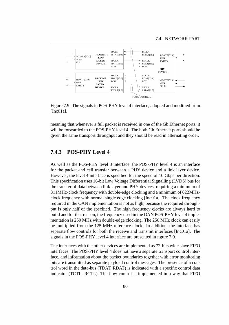
7.4. NETWORK PART
TSCLKTSTAT[1:0]
TDCLKTDAT[15:0]TCTL
WDATA[72:0]WENFULL
TRANSMITLINK
LAYERDEVICE
RDCLKRDAT[15:0]RCTL
RSCLKRSTAT[1:0]
RDATA[72:0]RENEMPTY
RECEIVELINK
LAYERDEVICE
RDCLKRDAT[15:0]RCTL
RSCLKRSTAT[1:0]
TSCLKTSTAT[1:0]
TDCLKTDAT[15:0]TCTL
RDATA[72:0]RENEMPTY
WDATA[72:0]WENFULL
PHYDEVICE
FLOW CONTROL
Figure 7.9: The signals in POS-PHY level 4 interface, adopted and modified from[Inc01a].
meaning that whenever a full packet is received in one of the Gb Ethernet ports, itwill be forwarded to the POS-PHY level 4. The both Gb Ethernet ports should begiven the same transport throughput and they should be read in alternating order.
7.4.3 POS-PHY Level 4
As well as the POS-PHY level 3 interface, the POS-PHY level 4 is an interfacefor the packet and cell transfer between a PHY device and a link layer device.However, the level 4 interface is specified for the speed of 10 Gbps per direction.This specification uses 16-bit Low Voltage Differential Signalling (LVDS) bus forthe transfer of data between link layer and PHY devices, requiring a minimum of311MHz-clock frequency with double-edge clocking and a minimum of 622MHz-clock frequency with normal single edge clocking [Inc01a]. The clock frequencyrequired in the OAN implementation is not as high, because the required through-put is only half of the specified. The high frequency clocks are always hard tobuild and for that reason, the frequency used in the OAN POS-PHY level 4 imple-mentation is 250 MHz with double-edge clocking. The 250 MHz clock can easilybe multiplied from the 125 MHz reference clock. In addition, the interface hasseparate flow controls for both the receive and transmit interfaces [Inc01a]. Thesignals in the POS-PHY level 4 interface are presented in figure 7.9.
The interfaces with the other devices are implemented as 72-bits wide slave FIFOinterfaces. The POS-PHY level 4 does not have a separate transport control inter-face, and information about the packet boundaries together with error monitoringbits are transmitted as separate payload control messages. The presence of a con-trol word in the data-bus (TDAT, RDAT) is indicated with a specific control dataindicator (TCTL, RCTL). The flow control is implemented in a way that FIFO
80
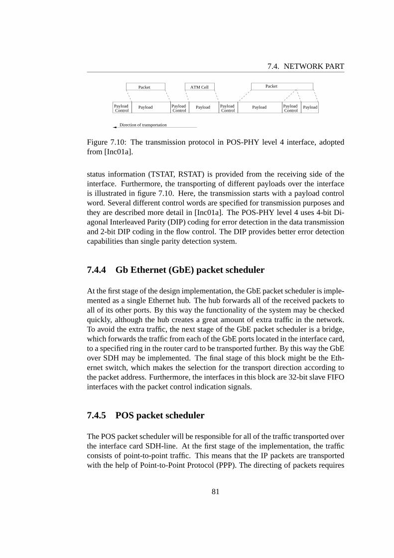
7.4. NETWORK PART
PayloadControl
Payload
ATM CellPacket
PayloadControl
Payload PayloadControl
PayloadControl
PayloadPayload
Packet
Direction of transportation
Figure 7.10: The transmission protocol in POS-PHY level 4 interface, adoptedfrom [Inc01a].
status information (TSTAT, RSTAT) is provided from the receiving side of theinterface. Furthermore, the transporting of different payloads over the interfaceis illustrated in figure 7.10. Here, the transmission starts with a payload controlword. Several different control words are specified for transmission purposes andthey are described more detail in [Inc01a]. The POS-PHY level 4 uses 4-bit Di-agonal Interleaved Parity (DIP) coding for error detection in the data transmissionand 2-bit DIP coding in the flow control. The DIP provides better error detectioncapabilities than single parity detection system.
7.4.4 Gb Ethernet (GbE) packet scheduler
At the first stage of the design implementation, the GbE packet scheduler is imple-mented as a single Ethernet hub. The hub forwards all of the received packets toall of its other ports. By this way the functionality of the system may be checkedquickly, although the hub creates a great amount of extra traffic in the network.To avoid the extra traffic, the next stage of the GbE packet scheduler is a bridge,which forwards the traffic from each of the GbE ports located in the interface card,to a specified ring in the router card to be transported further. By this way the GbEover SDH may be implemented. The final stage of this block might be the Eth-ernet switch, which makes the selection for the transport direction according tothe packet address. Furthermore, the interfaces in this block are 32-bit slave FIFOinterfaces with the packet control indication signals.
7.4.5 POS packet scheduler
The POS packet scheduler will be responsible for all of the traffic transported overthe interface card SDH-line. At the first stage of the implementation, the trafficconsists of point-to-point traffic. This means that the IP packets are transportedwith the help of Point-to-Point Protocol (PPP). The directing of packets requires
81
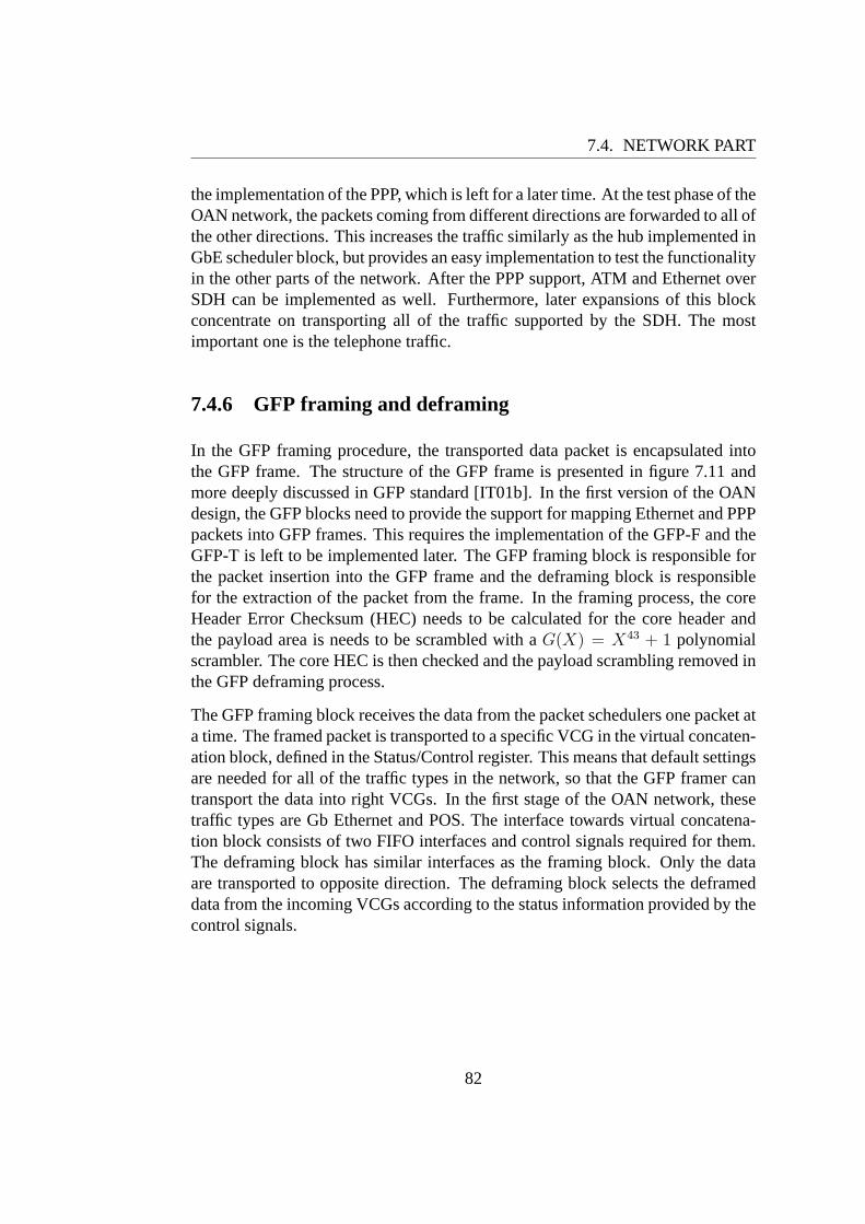
7.4. NETWORK PART
the implementation of the PPP, which is left for a later time. At the test phase of theOAN network, the packets coming from different directions are forwarded to all ofthe other directions. This increases the traffic similarly as the hub implemented inGbE scheduler block, but provides an easy implementation to test the functionalityin the other parts of the network. After the PPP support, ATM and Ethernet overSDH can be implemented as well. Furthermore, later expansions of this blockconcentrate on transporting all of the traffic supported by the SDH. The mostimportant one is the telephone traffic.
7.4.6 GFP framing and deframing
In the GFP framing procedure, the transported data packet is encapsulated intothe GFP frame. The structure of the GFP frame is presented in figure 7.11 andmore deeply discussed in GFP standard [IT01b]. In the first version of the OANdesign, the GFP blocks need to provide the support for mapping Ethernet and PPPpackets into GFP frames. This requires the implementation of the GFP-F and theGFP-T is left to be implemented later. The GFP framing block is responsible forthe packet insertion into the GFP frame and the deframing block is responsiblefor the extraction of the packet from the frame. In the framing process, the coreHeader Error Checksum (HEC) needs to be calculated for the core header andthe payload area is needs to be scrambled with aG(X) = X43 + 1 polynomialscrambler. The core HEC is then checked and the payload scrambling removed inthe GFP deframing process.
The GFP framing block receives the data from the packet schedulers one packet ata time. The framed packet is transported to a specific VCG in the virtual concaten-ation block, defined in the Status/Control register. This means that default settingsare needed for all of the traffic types in the network, so that the GFP framer cantransport the data into right VCGs. In the first stage of the OAN network, thesetraffic types are Gb Ethernet and POS. The interface towards virtual concatena-tion block consists of two FIFO interfaces and control signals required for them.The deframing block has similar interfaces as the framing block. Only the dataare transported to opposite direction. The deframing block selects the deframeddata from the incoming VCGs according to the status information provided by thecontrol signals.
82
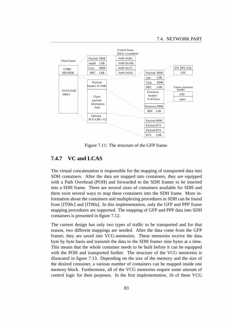
7.4. NETWORK PART
Extension MSB
HEC LSB
CID
Linear extensionheader
spare
Payload MSB
FCS LSB
Payload FCS
Payload FCS
CORE
PAYLOADAREA
Core MSB
HEC LSB
Control frame
0x00 (0x86)
0x00 (0xAB)
0x00 (0x31)
0x00 (0xE0)
IDLE (scrambled)
Payload MSB
type LSB
Type MSB
HEC LSB
HEADER
length LSB
Payload MSB
Clientpayload
informationfield
OptionalFCS (CRC−32)
Payloadheaders (4−64B)
Client frame
PTI
UPI
PFI EXI
Extensionheaders
0−60 bytes
Figure 7.11: The structure of the GFP frame.
7.4.7 VC and LCAS
The virtual concatenation is responsible for the mapping of transported data intoSDH containers. After the data are mapped into containers, they are equippedwith a Path Overhead (POH) and forwarded to the SDH framer to be insertedinto a SDH frame. There are several sizes of containers available for SDH andthere exist several ways to map these containers into the SDH frame. More in-formation about the containers and multiplexing procedures in SDH can be foundfrom [IT00c] and [IT00a]. In this implementation, only the GFP and PPP framemapping procedures are supported. The mapping of GFP and PPP data into SDHcontainers is presented in figure 7.12.
The current design has only two types of traffic to be transported and for thatreason, two different mappings are needed. After the data come from the GFPframer, they are saved into VCG-memories. These memories receive the databyte by byte basis and transmit the data to the SDH framer nine bytes at a time.This means that the whole container needs to be built before it can be equippedwith the POH and transported further. The structure of the VCG memories isillustrated in figure 7.13. Depending on the size of the memory and the size ofthe desired container, a various number of containers can be mapped inside onememory block. Furthermore, all of the VCG memories require some amount ofcontrol logic for their purposes. In the first implementation, 16 of these VCG
83
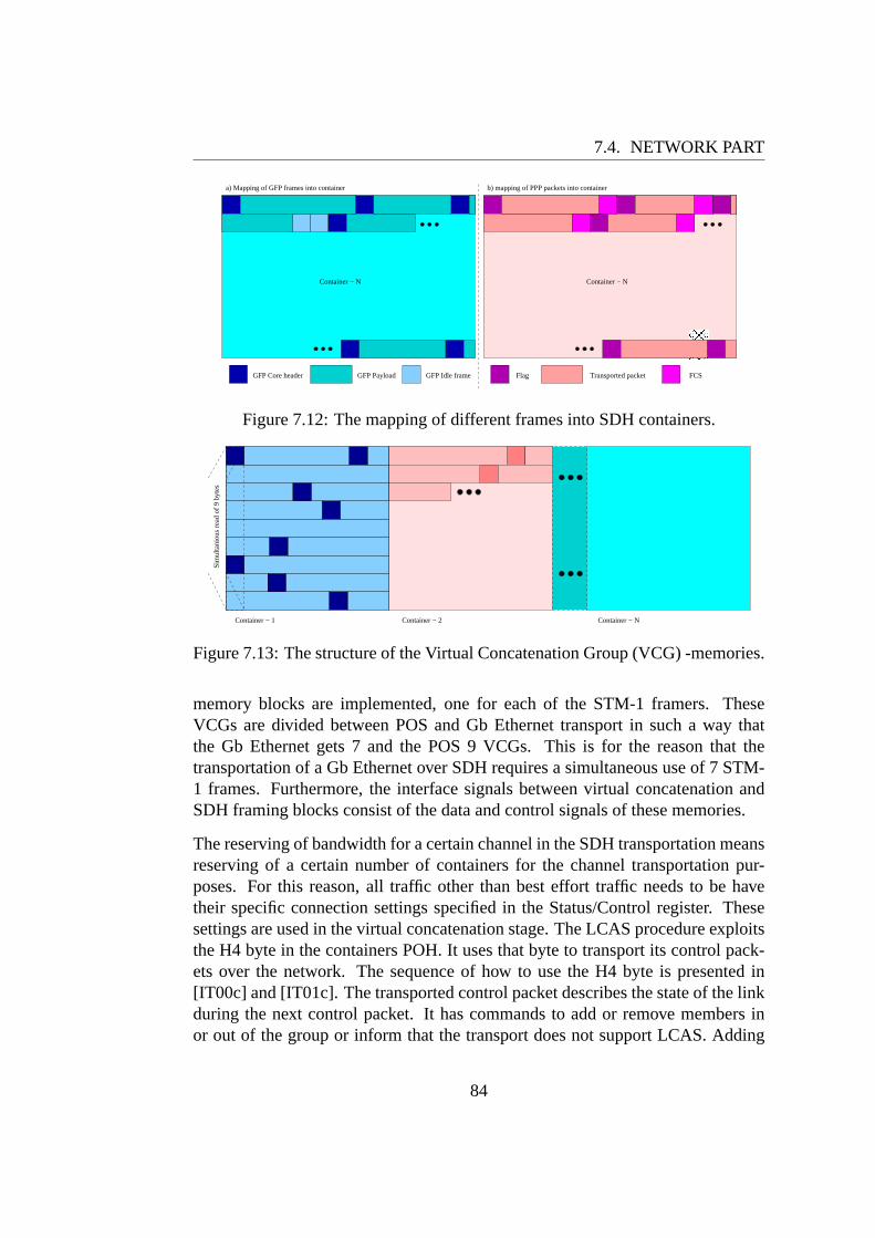
7.4. NETWORK PART
���������
���������
GFP Core header GFP Payload GFP Idle frame Flag FCSTransported packet
Container − N Container − N
a) Mapping of GFP frames into container b) mapping of PPP packets into container
Figure 7.12: The mapping of different frames into SDH containers.
Container − 1 Container − NContainer − 2
Sim
ulta
niou
s re
ad o
f 9
byte
s
Figure 7.13: The structure of the Virtual Concatenation Group (VCG) -memories.
memory blocks are implemented, one for each of the STM-1 framers. TheseVCGs are divided between POS and Gb Ethernet transport in such a way thatthe Gb Ethernet gets 7 and the POS 9 VCGs. This is for the reason that thetransportation of a Gb Ethernet over SDH requires a simultaneous use of 7 STM-1 frames. Furthermore, the interface signals between virtual concatenation andSDH framing blocks consist of the data and control signals of these memories.
The reserving of bandwidth for a certain channel in the SDH transportation meansreserving of a certain number of containers for the channel transportation pur-poses. For this reason, all traffic other than best effort traffic needs to be havetheir specific connection settings specified in the Status/Control register. Thesesettings are used in the virtual concatenation stage. The LCAS procedure exploitsthe H4 byte in the containers POH. It uses that byte to transport its control pack-ets over the network. The sequence of how to use the H4 byte is presented in[IT00c] and [IT01c]. The transported control packet describes the state of the linkduring the next control packet. It has commands to add or remove members inor out of the group or inform that the transport does not support LCAS. Adding
84
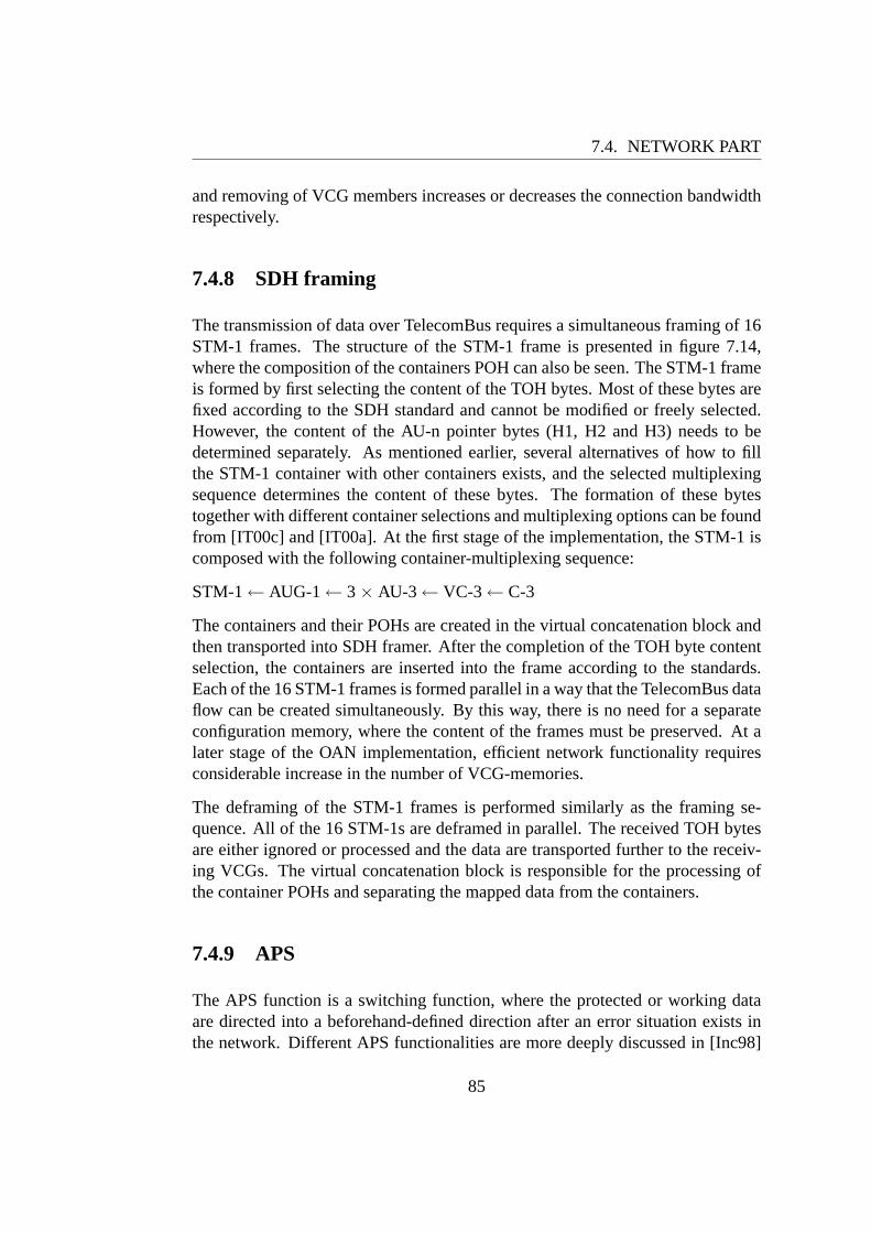
7.4. NETWORK PART
and removing of VCG members increases or decreases the connection bandwidthrespectively.
7.4.8 SDH framing
The transmission of data over TelecomBus requires a simultaneous framing of 16STM-1 frames. The structure of the STM-1 frame is presented in figure 7.14,where the composition of the containers POH can also be seen. The STM-1 frameis formed by first selecting the content of the TOH bytes. Most of these bytes arefixed according to the SDH standard and cannot be modified or freely selected.However, the content of the AU-n pointer bytes (H1, H2 and H3) needs to bedetermined separately. As mentioned earlier, several alternatives of how to fillthe STM-1 container with other containers exists, and the selected multiplexingsequence determines the content of these bytes. The formation of these bytestogether with different container selections and multiplexing options can be foundfrom [IT00c] and [IT00a]. At the first stage of the implementation, the STM-1 iscomposed with the following container-multiplexing sequence:
STM-1← AUG-1← 3× AU-3← VC-3← C-3
The containers and their POHs are created in the virtual concatenation block andthen transported into SDH framer. After the completion of the TOH byte contentselection, the containers are inserted into the frame according to the standards.Each of the 16 STM-1 frames is formed parallel in a way that the TelecomBus dataflow can be created simultaneously. By this way, there is no need for a separateconfiguration memory, where the content of the frames must be preserved. At alater stage of the OAN implementation, efficient network functionality requiresconsiderable increase in the number of VCG-memories.
The deframing of the STM-1 frames is performed similarly as the framing se-quence. All of the 16 STM-1s are deframed in parallel. The received TOH bytesare either ignored or processed and the data are transported further to the receiv-ing VCGs. The virtual concatenation block is responsible for the processing ofthe container POHs and separating the mapped data from the containers.
7.4.9 APS
The APS function is a switching function, where the protected or working dataare directed into a beforehand-defined direction after an error situation exists inthe network. Different APS functionalities are more deeply discussed in [Inc98]
85
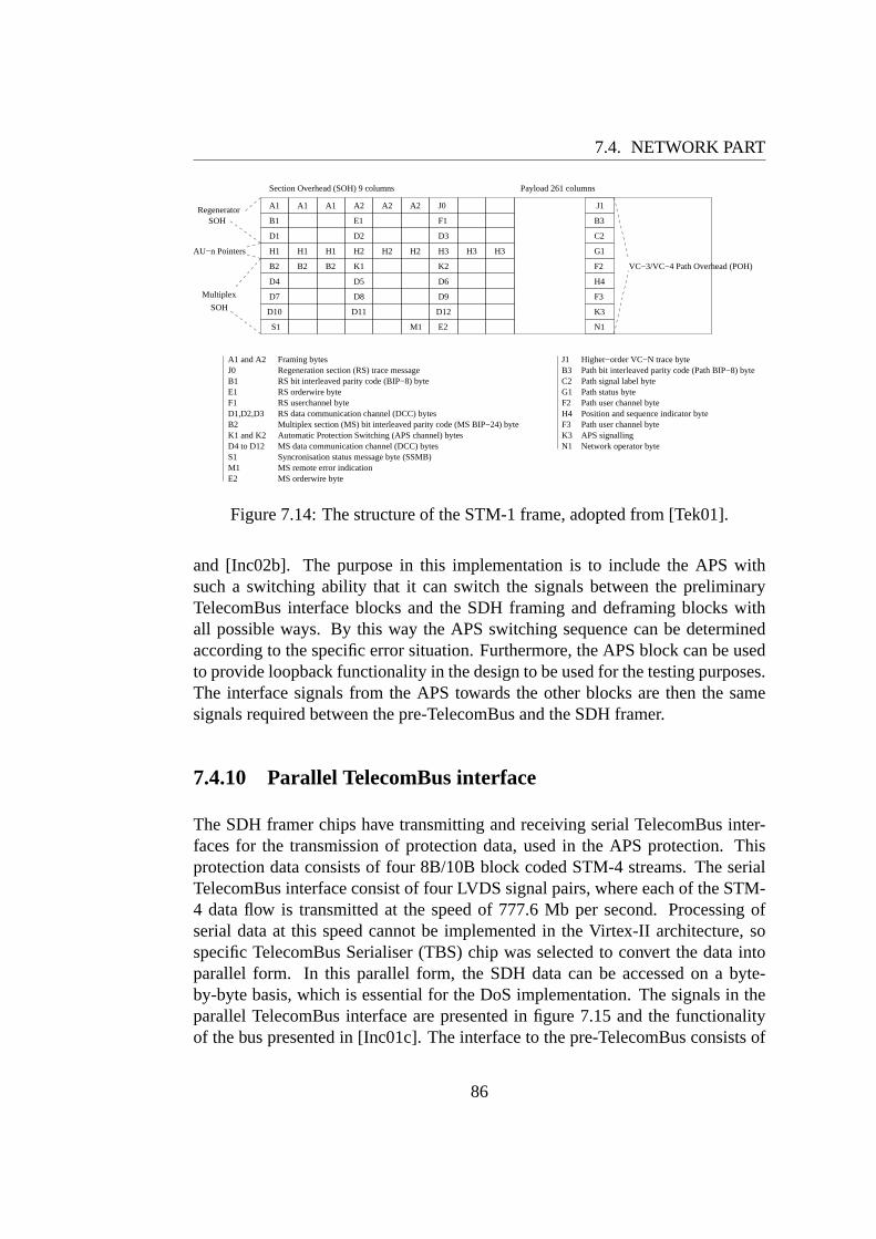
7.4. NETWORK PART
A1 and A2J0B1E1F1D1,D2,D3B2K1 and K2D4 to D12S1M1E2
Framing bytes
RS orderwire byteRS userchannel byte
RS bit interleaved parity code (BIP−8) byte
Automatic Protection Switching (APS channel) bytes
Syncronisation status message byte (SSMB)MS remote error indicationMS orderwire byte
Regeneration section (RS) trace message
RS data communication channel (DCC) bytesMultiplex section (MS) bit interleaved parity code (MS BIP−24) byte
MS data communication channel (DCC) bytes
J1B3C2G1F2H4F3K3N1
Higher−order VC−N trace bytePath bit interleaved parity code (Path BIP−8) bytePath signal label bytePath status bytePath user channel bytePosition and sequence indicator bytePath user channel byteAPS signallingNetwork operator byte
A1
B1
D1
H1
A1 A1
H1 H1
J0
D2 D3
D4
D10
D7
D12
E1
A2 A2 A2
H2 H2 H3 H3
B2 B2B2
H2
F1
H3
K2
D6
D9
E2M1
D11
D8
D5
K1
S1
SOH
Multiplex
AU−n Pointers
RegeneratorSOH
Section Overhead (SOH) 9 columns Payload 261 columns
J1
G1
C2
B3
F2
H4
F3
K3
N1
VC−3/VC−4 Path Overhead (POH)
Figure 7.14: The structure of the STM-1 frame, adopted from [Tek01].
and [Inc02b]. The purpose in this implementation is to include the APS withsuch a switching ability that it can switch the signals between the preliminaryTelecomBus interface blocks and the SDH framing and deframing blocks withall possible ways. By this way the APS switching sequence can be determinedaccording to the specific error situation. Furthermore, the APS block can be usedto provide loopback functionality in the design to be used for the testing purposes.The interface signals from the APS towards the other blocks are then the samesignals required between the pre-TelecomBus and the SDH framer.
7.4.10 Parallel TelecomBus interface
The SDH framer chips have transmitting and receiving serial TelecomBus inter-faces for the transmission of protection data, used in the APS protection. Thisprotection data consists of four 8B/10B block coded STM-4 streams. The serialTelecomBus interface consist of four LVDS signal pairs, where each of the STM-4 data flow is transmitted at the speed of 777.6 Mb per second. Processing ofserial data at this speed cannot be implemented in the Virtex-II architecture, sospecific TelecomBus Serialiser (TBS) chip was selected to convert the data intoparallel form. In this parallel form, the SDH data can be accessed on a byte-by-byte basis, which is essential for the DoS implementation. The signals in theparallel TelecomBus interface are presented in figure 7.15 and the functionalityof the bus presented in [Inc01c]. The interface to the pre-TelecomBus consists of
86

7.4. NETWORK PART
OVERHEAD
DATA
OVERHEAD
DATA
Data[32:1]Control[14:1]
Data[32:1]Control[14:1]
OTAIS[4:1]
OPAIS[4:1]
ID[4:1][7:0]IDP[4:1]IPL[4:1]IJ0J1[4:1]IPAIS[4:1]ITV5[4:1]ITPL[4:1]ITAIS[4:1]
OD[4:1][7:0]ODP[4:1]OPL[4:1]OJ0J1[4:1]
OTV5[4:1]OTPL[4:1]
OCOUT[4:1]
ParallelTelecomBus
To pre−telecombus
Figure 7.15: The signals in the parallel TelecomBus interface, adopted and modi-fied from [Inc01c].
control and data signals, discussed more detail in next section.
7.4.11 Preliminary TelecomBus interface
The preliminary TelecomBus interface is used to transport the TelecomBus datafrom the larger FPGA to the smaller FPGA in the router card. Because there areonly a limited number of signals available between the devices, specific protocolneeded to be developed for the data transportation process, which provides in-formation from the transported data on a byte by byte basis. As it was discussedin the previous chapter, the connection between FPGAs has 184 signals to be usedfor the pre-TelecomBus interface. These signals are divided between four inter-faces, leaving 46 signals to be used in each of them. 32 of these signals are neededfor the transportation of the data and 2 signals are left for the flow control. Thismeans that the interface can use 12 signals to pass the byte basis information.
The required information in the TelecomBus can be divided into eight controlcharacters presented in table 7.6. This means that each of the bytes transpor-ted over the pre-TelecomBus interface can be marked with a special TelecomBuscharacter. By this way, the transportation of the TelecomBus data can be done syn-chronously over the FPGA limits, which means that the pre-TelecomBus signalsare only connected from the APS block to the parallel TelecomBus block and thecontrol characters are coded and decoded in these blocks respectively. So there isno need for a separate TelecomBus converter as presented in figure 7.3.
87
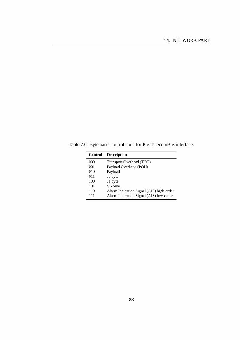
7.4. NETWORK PART
Table 7.6: Byte basis control code for Pre-TelecomBus interface.
Control Description
000 Transport Overhead (TOH)001 Payload Overhead (POH)010 Payload011 J0 byte100 J1 byte101 V5 byte110 Alarm Indication Signal (AIS) high-order111 Alarm Indication Signal (AIS) low-order
88

Chapter 8
Conclusions
In this thesis, the present structure of communication networks was studied andthe requirements for future communication networks identified. Based on theserequirements, a programmable logic design for an optical access network waspresented to be implemented inside the Field Programmable Gate Arrays (FPGAs)of the OAN project network prototype.
8.1 Results
Today, three separate communication networks can be identified, telephony, datacommunications and broadcast networks. This overlaid network structure is com-plex to maintain, which causes extra cost to the operators. Furthermore, the com-plexity in the metropolitan area networks has become a bottleneck for the de-velopment of the transportation speed in the communication networks, and theemerging real-time and streaming media services cannot be supported by thesenetworks. For these reasons, the development of communication networks isheading towards convergence. Converged networks are easier to maintain thanthe conventional networks, and all different access technologies are to be sup-ported in hybrid transport systems. The Data over SDH (DoS) is one solutionpresented for the hybrid transport system in converged networks. It consists ofseparate transport and access network interfaces and a flexible Generic FramingProcedure (GFP) layer between them. This layer enables mapping of differentaccess technologies over different transport technologies. In DoS, the networkQuality of Service (QoS) is implemented with the efficient bandwidth reservationsystem provided by Virtual Concatenation (VC) and Link Capacity Adjustment
89

8.2. FUTURE DEVELOPMENTS
Scheme (LCAS). Furthermore, the utilisation of the Wavelength Division Multi-plexing (WDM) enables faster increase of bandwidth in the networks.
The OAN project concentrates on developing the metropolitan area networkingand based on the research, an optical feeder network prototype is being built. Thisprototype exploits the DoS scheme, which is implemented by programming thethree FPGAs attached in the prototype board. The design presented in this thesisis a simplified version of the fully operational network. However, the design isstructured in such a way that a fully operational network could be implementedonly by updating the design blocks. The reason for simplified design implementa-tion was the purpose to get the OAN test network operational as soon as possible.The use of the FPGAs allows the modification of the program over and over again,and to avoid problems, it is good to start with a small number of functionalities.Furthermore, the purpose was to present the simplified design with the amount ofdetails typical of this type of design specification, but it was not possible withinthe scope of the thesis. For this reason, some of the functionalities of the designare presented lightly and the reader is guided to the source literature for moreinformation.
8.2 Future developments
In the future, the functionality of the OAN test network should be increased. Afterthe first version of the OAN test network is operational, additions to the programscan be made easily. The first additions should be the fully operational Gb Ethernetswitch and fully functional SDH transport environment. This means that moreVirtual Concatenation Groups (VCGs) need to be added for the VC and the restof the SDH multiplexing sequences implemented. The connection between routerand interface cards needs to be redesigned so that multiple cards can be connectedtogether in both sides of the prototype. Furthermore, some improvements to theinterface card register access procedure should also be made.
The network functionality is implemented in the larger FPGA in the router card,and the smaller FPGA is left almost unused. This unbalanced utilisation is notideal, and some improvements should be made, especially when the networkfunctionality is increased. The resources available in the larger FPGA may betoo scarce for the future development, especially more internal memory might beneeded in a later stage. For this reason, better resource utilisation for the smallerFPGA seems unavoidable. At least one possible solution exists for the purpose.It seems that the ring operations may be divided in such a way that the east ringoperations may be implemented in the smaller FPGA and the west ring operations
90
8.2. FUTURE DEVELOPMENTS
in the larger FPGA. However, some difficulties with other functionalities may oc-cur with this solution. At least the APS cannot be implemented similarly to thecurrent design. For this reason, all the possible changes need to be consideredseparately.
The design of the implemented prototype was almost a success from the FPGAprogramming point of view. Some of the physical structures realised in the proto-type brought difficulties in the program design, but mostly the physical solutionswere proven competent. One problem was the division of the network functional-ities between the two FPGAs in the router card. A solution for the problem wasfound, but it was not nearly a perfect one. Using only one FPGA in the routercard would have made designing of the program easier and should be consideredat least in the next revision of the prototype. In this revision it was not possiblebecause of the large number of connection points needed, but the FPGAs havebecome larger since then, and it might be possible to have all connected into oneFPGA. Furthermore, today there are SDH framing chips available on the market,which have the DoS functionality already implemented. Selecting this kind ofchip to replace the SDH framer chip, TelecomBus chip and the DoS implementa-tion in the FPGA, could decrease the number of connections needed in the routercard. In addition, GFP has a support for direct Gb Ethernet transport, and the needfor separate Gb Ethernet framer chip in the interface card should be considered inthe next revision of the prototype.
91
Bibliography
[All01] Resilient Packet Ring Alliance. An Introduction to Resilient PacketRing Technology. White Paper, http://www.rpralliance.com, Octo-ber 2001.
[All03] Resilient Packet Ring Alliance. A Summary and Over-view of the IEEE 802.17 RPR Standard. White Paper,http://www.rpralliance.com, August 2003.
[And02] Per O. Andersson. Optical Network Trends. Presentation on Sun-ets Tekniska Rerensgrup, http://kokbok.sunet.se/trefpunkt/, March2002. TREFpunkt Nr 6, Uppsala 13.03.2002.
[Arm97] H. Armbruster. Information infrastructures and multimedia commu-nications: different approaches of the telephone, data, and radio/TVworlds.IEEE Communications Magazine, 35(9):92–101, September1997.
[ASFG+98] Daniel Y. Al-Salameh, Mohammad T. Fatehi, William J. Gartner,Stan Lumish, Bruce L. Nelson, and Kamal K. Raychaudhri. OpticalNetworking.Bell Labs Technical Journal, January-March 1998.
[Bai03] Brian Bailey. Total Verification. Mentor Graphics, Verification Sem-inars 2003, 10. March 2003. Espoo, Finland.
[Bel03] Mary Bellis. The History of the Telegraph and Tele-graphy. Webpages of What you need to know, 2003.http://inventors.about.com/library/inventors/bltelegraph.htm.
[Ben02] K. Bengi. Access protocols for an efficient optical packet-switchedmetropolitan area ring network supporting ip datagrams. InElev-enth International Conference on Computer Communications andNetworks, 2002, pages 284–289. IEEE, 2002.
92
BIBLIOGRAPHY
[Ber00] Janick Bergeron.Writing Testbenches Functional Verification ofHDL Models. Kluwer Academic Publishers, 2000.
[BP01] Richard Barr and Raymond A. Patterson. Grooming telecommunic-ations networks.Optical Networks Magazine, 2(3):20–23, May/June2001.
[Bre02] Stefano Bregni.Synchronization of Digital Telecommunication Net-works. John Wiley & Sons, Ltd., 2002.
[BRM01] Paul Bonenfant and Antonio Rodriguez-Moral. Framing Techniquesfor IP over Fiber.IEEE Network Magazine, July/August 2001.
[BRM02] Paul Bonenfant and Antonio Rodriguez-Moral. Generic FramingProcedure (GFP): The Catalyst for Efficient Data over Transport.IEEE Communications Magazine, 40(5):72–75, May 2002.
[Cav00] Dirceu Cavendish. Evolution of Optical Transport Technologies:From SONET/SDH to WDM. IEEE Communications Magazine,2000.
[Com01] Terawave Communications. Next Generation Passive Optical Net-works. White paper, http://www.terawave.com, January 2001.
[Con89] J.K. Conlisk. Topology and survivability of future transport net-works. In Global Telecommunications Conference, 1989, and Ex-hibition. ’Communications Technology for the 1990s and Beyond’.GLOBECOM ’89., pages 826–834 vol.2, 27-30 November 1989.
[Cor99] Actel Corporation. Actel HDL Coding. Actel Corporation StyleGuide, October 1999.
[CSK88] G.H. Clapp, M. Singh, and S. Karr. Metropolitan area network archi-tecture and services. InCommunications for the Information Age.,volume 3, pages 1246–1254. Global Telecommunications Confer-ence, 1988, and Exhibition., IEEE, 28 Nov-1 Dec 1988. ConferenceRecord, GLOBECOM ’88.
[DGA+99] P. Demeester, M. Gryseels, A. Autenrieth, C. Brianza, L. Castagna,R. Signorelli, G.and Clemenfe, M. Ravera, A. Lajszczyk, D. Ja-nukowicz, K. Van Doorselaere, and Y. Harada. Resilience in mul-tilayer networks. IEEE Communications Magazine, 37(8):70–76,August 1999.
93

BIBLIOGRAPHY
[DHL+03] H.J.S. Dorren, M.T. Hill, Y. Liu, N. Calabretta, A. Srivatsa, F.M.Huijskens, H. de Waardt, and G.D. Khoe. Optical packet switchingand buffering by using all-optical signal processing methods.Light-wave Technology, 21(1):2–12, 2003.
[Ele01] Samsung Electronics. 512Kx36 Pipelined NtRAM (K7N163645M).Datasheet, February 2001.
[EUa] IST programme European Union. DAVID. Projects webpage,http://david.com.dtu.dk/. Duration July 2000 -July 2003.
[EUb] IST programme European Union. HARMONICS. Projects webpage,http://www.ist-harmonics.net/. Duration: April 2000 - April 2003.
[fS94] International Organisation for Standardisation. Open systems inter-connection in general. ISO standard, 1994. ISO/IEC 7498-1:1994.
[GCC92] M. Gerla, P. Camarda, and G. Chiaretti. Fault tolerant PON topo-logies. InINFOCOM ’92. Eleventh Annual Joint Conference of theIEEE Computer and Communications Societies, pages 49–56 vol.1.IEEE, 4-8 May 1992.
[GJS03] J. Gozdecki, A. Jajszczyk, and R. Stankiewicz. Quality of ser-vice terminology in IP networks.IEEE Communications Magazine,41(3):153–159, March 2003.
[Gor00] Walter Goralski.SONET Second Edition. McGraw-Hill, 2000.
[GR00] O. Gerstel and R. Ramaswami. Optical layer survivability-an imple-mentation perspective.IEEE Journal on Selected Areas in Commu-nications, 18(10):1885–1899, October 2000.
[GRF02] O. Gerstel, R. Ramaswami, and S. Foster. Merits of hybrid opticalnetworking. InOptical Fiber Communication Conference and Ex-hibit, pages 33–34. OFC 2002, 17-22 March 2002.
[Gro] Broadband Networks Group. Access Networks. Webpage.http://www.opto.eee.strath.ac.uk/BBN/.
[Gro03] IEEE 802.17 Resilient Packet Ring Working Group. IEEE 802.17Resilient Packet Ring (RPR) Standard. IEEE Standards, May 12th2003. Draft ver. 2.2.
94
BIBLIOGRAPHY
[GW02] Steven S. Gorshe and Trevor Wilson. Transparent Generic Fram-ing Procedure (GFP): A Protocol for Efficient Transport of Block-Coded Data through SONET/SDH Networks.IEEE Communica-tions Magazine, 40(5):88–95, May 2002.
[HM02] Pin-Han Ho and Hussein T. Mouftah. A Framework of Scalable Op-tical Metropolitan Networks for Improving Survivability and Classof Service.IEEE Network, 16(4):29–35, July/August 2002.
[HV02] Enrique Hernandez-Valencia. Hybrid Transport Solutions forTDM/Data Networking Services.IEEE Communications Magazine,40(5):104–112, May 2002.
[HVSZ02] Enrique Hernandez-Valencia, Michael Scholten, and Zhenyu Zhu.The Generic Framing Procedure (GFP): An Overwiev.IEEE Com-munication Magazine, 40(5):63–71, May 2002.
[Inc98] PMC-Sierra Inc. Network Survivability Using Automatic ProtectionSwitching (APS) over SONET/SDH Point-to-Point and Ring Net-works. Application note, PMC-960505, February 1998. Issue 3.
[Inc00] PMC-Sierra Inc. POS-PHY Level 3 Saturn Compatible Packet OverSonet Interface Specification For Physical And Link Layer Devices.Compatibility Specification, June 200. Issue 4.
[Inc00a] Xicor Inc. X9110 Single Digitally-Controlled (XDCP) Poten-tiometer. Datasheet, November 2000. Revision 1.1.4.
[Inc00b] Xicor Inc. X9221 Dual Digitally-Controlled Potentiometer (XDCP).Datasheet, June 2000. Revision 1.0.
[Inc00c] Xilinx Inc. Virtex-2 Platform FPGA Handbook, December 2000.
[Inc01a] PMC-Sierra Inc. A Saturn Packet And Cell Interface SpecificationFor OC192 SONET/SDH And 10 Gigabit Ethernet. Interface Spe-cification, February 2001. Issue 6.
[Inc01b] PMC-Sierra Inc. PM3386 S/UNI-2xGE Dual Gigabit Ethernet Con-troller. Datasheet, February 2001. Issue 6.
[Inc01c] PMC-Sierra Inc. PM5310 TBS TelecomBus Serializer. Datasheet,November 2001. Issue 7.
[Inc02a] PMC-Sierra Inc. PM5381 S/UNI-2488 User Network Interface for2488 Mb/s. Datasheet, April 2002. Issue 3.
95
BIBLIOGRAPHY
[Inc02b] PMC-Sierra Inc. SONET/SDH Automatic Protection Switching.Application note, PMC-2020827, May 2002. Issue 1.
[Inc02c] Xilinx Inc. Next Generation Networking Technologies. Presentationin Metro-Optical Networking Forum, July 2002.
[Inc03] Xilinx Inc. Xilinx 5 Software Manuals and Help.http://www.xilinx.com/support, 2003.
[IT98] ITU-T. Broadband Optical Access Systems Based on Passive OpticalNetworks (PON). Recommendation G.983.1, October 1998.
[IT00a] ITU-T. Characteristics of synchronous digital hierarchy (SDH)equipment functional blocks. ITU-T Recommendation G.783, Oc-tober 2000.
[IT00b] ITU-T. Framework for Optical Transport Network Recommenda-tions. ITU-T Recommendation G.871/Y.1301, October 2000.
[IT00c] ITU-T. Network node interface for the synchronous digital hierarchy(SDH). ITU-T Recommendation G.707/Y.1322, October 2000.
[IT00d] ITU-T. ONT Management and Control interface Specification forATM-PON. Recommendation G.983.2, April 2000.
[IT01a] ITU-T. A Broadband Optical Access System with Increased ServiceCapability by Wavelength Allocation. Recommendation G.983.3,March 2001.
[IT01b] ITU-T. Generic Framing Procedure (GFP). ITU-T RecommendationG.7041/Y.1303, December 2001.
[IT01c] ITU-T. Link capacity adjustment scheme (LCAS) for virtual concat-enated signals. ITU-T Recommendation G.7042/Y.1305, November2001.
[ITU02] ITU-T, study group 15. Recommendation of G.GPON.gsr - Gen-eral Characteristics for Gigabit-capable Passive Optical Networks(GPON), December 2002.
[Kai02] Antti Kaikkonen. Läpinäkyvä kaupunkialueen aallon-pituuskanavoitu rengasverkko. Master’s thesis, Helsinki Universityof Technology, December 2002.
96

BIBLIOGRAPHY
[KP02] Glen Kramer and Gerry Pesavento. Ethernet Passive Optical Net-work (EPON): Building a Next-Generation Optical Access Network.IEEE Communications Magazine, 40(2):66–73, February 2002.
[Lab00] Stanford University Optical Communications Re-search Laboratory. IP-HORNET. Projects webpage,http://wdm.stanford.edu/iphornet/iphornet.html, 2000.
[LDA +98] P. Lagasse, P. Demeester, A. Ackaert, W. Van Parys, B. VanCaenegem, M. O’Mahony, K. Stubkjaer, and J. Benoit. Roadmaptowards the Optical Communication Age. A European view bythe HORIZON project and the ACTS Photonic Domain, June 1998.Draft Edition.
[LGP01] Ana Lardies, Rakesh Gupta, and Raymond A. Patterson. TrafficGrooming in a Multi-layer Network.Optical Networks Magazine,2(3):91–99, May/June 2001.
[MBK01] A.R. Moral, P. Bonenfant, and M. Krishnaswamy. The optical In-ternet: architectures and protocols for the global infrastructure oftomorrow. IEEE Communications Magazine, 39(7):152–159, July2001.
[MF01] Y. Maeda and R Feigel. A standardization plan for broadband accessnetwork transport. IEEE Communications Magazine, 39(7):166–172, July 2001.
[MHPG91] K.S. Meier-Hellstern, G.P. Pollini, and D.J. Goodman;. A wirelessservice for the IEEE 802.6 metropolitan area network. InCount-down to the New Millennium. Featuring a Mini-Theme on: PersonalCommunications Services, volume 3, pages 1964 –1968. IEEE, 2-5Dec 1991.
[Mol88] James F. Mollenauer. Standards for Metropolitan Area Networks.IEEE Communication Magazine, 26(4), April 1988.
[Muk97] Biswanath Mukherjee.Optical Communication Networks. McGraw-Hill, 1997.
[MYMN02] Kureina Murakami, Su-Hun Yun, Osamu Matsuda, and Mo-too Nishihara. New Transport Services for Next-GenerationSONET/SDH Systems.IEEE Communications Magazine, 40(5):80–87, May 2002.
97

BIBLIOGRAPHY
[Net02] Flexlight Networks. GPON - The Next Big Thing in Optical Ac-cess Network: A Comparison Between EPON, APON and theEmerging GPON Technology. White paper, http://www.flexlight-networks.com, August 2002.
[Net03] Foundry Networks. Metropolitan Area Networks. Application note,2003.
[Ope02] OpenCores.org. OpenCores Coding Guidelines.http://www.opencores.org/, August 2002. Rev. 1.1.
[OSG02] Fredrik Olsson, Jim Shupenis, and Alistair Gunn. Virtual Concaten-ation + LCAS. Technical report, Agilent Technologies, 2002.
[Par02] Eugene Park. Error Monitoring for Optical Metropolitan NetworkServices.IEEE Communication Magazine, 40(2):104–109, February2002.
[Pro97] MAXIM Integrated Products. MAXIM +5V, low-power, voltage-output, serial 12-bit DAC MAX531. Datasheet, February 1997. Re-vision 6.
[Pro01] MAXIM Integrated Products. MAXIM +2,7V, low-power, 4-channel, serial 12-bit ADC MAX1247. Datasheet, October 2001.Revision 2.
[Sep02] Kari Seppänen. Transport services for converging networks. Licen-tiate’s Thesis, October 2002. Helsinki University of Technology.
[SK03] Gerry Pasavento Senior and Mark Kelsey. Gigabit Ethernet PassiveOptical Networks. Wamin Optocomm Mfg. Corporation Publica-tion, http://www.wamin.com, 2003.
[SS99] A.A.M. Saleh and J.M. Simmons. Architectural principles of opticalregional and metropolitan access networks.Lightwave Technology,17(12):2431–2448, December 1999.
[STS02] Toshiya Sato, Hiroki Takesue, and Toshihiko Sugie. Photonic Ac-cess and Metropolitan Area Networks for Broadband Services. InTransparent Optical Networks, 2002, Proceedings of the 2002 4thInternational Conference, pages 12–15, 2002.
[SZHVH02] Mike Scholten, Zhenyu Zhu, Enrique Hernandez-Valencia, and JohnHawkings. Data Transport Applications Using GFP.IEEE Commu-nications Magazine, 40(5):96–103, May 2002.
98

BIBLIOGRAPHY
[Tec] Agilent Technologies. An overview of ITU-T G.709. ApplicationNote 1379. http://www.agilent.com/.
[Tec00] PLX Technology. PCI 9030 Data Book. Data Book,http://www.plxtech.com, April 2000. Version 1.0.
[Tec02] VTT Information Technology. Communications Technologies. TheVTT Roadmaps. VTT Research notes 2146, 2002.
[Tek01] Tektronix. SDH Telecommunications Standard Primer. Applicationnote, August 2001. http://www.tektronix.com/.
[YJH+00] Qiao Yaojun, Qi Jiang, Pu Hongtu, Chen Shuqiang, and GuanKejian. A New Scheme for WDM-Based Passive Optical Access-network. Proceedings of ICCT2000, webpage http://www.ifip.or.at/,2000. Session S59.4.
[YYMD01] Shun Yao, S.J.B. Yoo, B. Mukherjee, and S. Dixit. All-OpticalPacket Switching for Metropolitan Area Networks: Opportunitiesand Challenges.IEEE Communication Magazine, 39(3):142–148,March 2001.
[ZD02] H. Zhang and A. Durresi. Differentiated multi-layer survivability inIP/WDM networks. InNetwork Operations and Management Sym-posium (NOMS), pages 681–694. IEEE/IFIP, 2002.
99