programming examples for the tms320f281x - texas instruments
TRANSCRIPT

Application ReportSPRA876A - January 2003 – Revised April 2003
1
Programming Examples for the TMS320F281x eCANHareesh Janakiraman Advanced Embedded Control Group
ABSTRACT
The TMS320F28x (TMS320F2812 and TMS320F2810) series of digital signal processor(DSP) controllers feature an on-chip enhanced Controller Area Network (eCAN) module.This module is a full-CAN controller, compliant with CAN specification 2.0B. This applicationreport contains several programming examples to illustrate how the eCAN module is set upfor different modes of operation. The objective is to help you come up to speed quickly inprogramming the eCAN. All programs have been extensively commented to aid easyunderstanding. The CANalyzer tool from Vector CANtech, Inc. was used to monitor andcontrol the bus operation. All projects and CANalyzer configuration files are included in theattached SPRA876.zip file.
Contents
1 Introduction 2. . . . . . . . . . . . . . . . . . . . . . . . . . . . . . . . . . . . . . . . . . . . . . . . . . . . . . . . . . . . . . . . . . . . . . . . . 1.1 TMS320F28x eCAN features 2. . . . . . . . . . . . . . . . . . . . . . . . . . . . . . . . . . . . . . . . . . . . . . . . . . . . . . 1.2 3.3-V CAN Transceivers 2. . . . . . . . . . . . . . . . . . . . . . . . . . . . . . . . . . . . . . . . . . . . . . . . . . . . . . . . . . .
2 Programs 3. . . . . . . . . . . . . . . . . . . . . . . . . . . . . . . . . . . . . . . . . . . . . . . . . . . . . . . . . . . . . . . . . . . . . . . . . . . 2.1 DSP28_ECan.c 4. . . . . . . . . . . . . . . . . . . . . . . . . . . . . . . . . . . . . . . . . . . . . . . . . . . . . . . . . . . . . . . . . . 2.2 Back2bak.c 7. . . . . . . . . . . . . . . . . . . . . . . . . . . . . . . . . . . . . . . . . . . . . . . . . . . . . . . . . . . . . . . . . . . . . . 2.3 MBXRAMRW.c 11. . . . . . . . . . . . . . . . . . . . . . . . . . . . . . . . . . . . . . . . . . . . . . . . . . . . . . . . . . . . . . . . . . 2.4 TXLOOP.c 13. . . . . . . . . . . . . . . . . . . . . . . . . . . . . . . . . . . . . . . . . . . . . . . . . . . . . . . . . . . . . . . . . . . . . . 2.5 RXLOOP.c 14. . . . . . . . . . . . . . . . . . . . . . . . . . . . . . . . . . . . . . . . . . . . . . . . . . . . . . . . . . . . . . . . . . . . . . 2.6 TRPRTSTP.c 16. . . . . . . . . . . . . . . . . . . . . . . . . . . . . . . . . . . . . . . . . . . . . . . . . . . . . . . . . . . . . . . . . . . 2.7 DLCTX.c 20. . . . . . . . . . . . . . . . . . . . . . . . . . . . . . . . . . . . . . . . . . . . . . . . . . . . . . . . . . . . . . . . . . . . . . . 2.8 DLCRX.c 22. . . . . . . . . . . . . . . . . . . . . . . . . . . . . . . . . . . . . . . . . . . . . . . . . . . . . . . . . . . . . . . . . . . . . . . 2.9 DBOTX.c 23. . . . . . . . . . . . . . . . . . . . . . . . . . . . . . . . . . . . . . . . . . . . . . . . . . . . . . . . . . . . . . . . . . . . . . . 2.10 DBORX.c 25. . . . . . . . . . . . . . . . . . . . . . . . . . . . . . . . . . . . . . . . . . . . . . . . . . . . . . . . . . . . . . . . . . . . . . . 2.11 MBXWDIF.c 28. . . . . . . . . . . . . . . . . . . . . . . . . . . . . . . . . . . . . . . . . . . . . . . . . . . . . . . . . . . . . . . . . . . . . 2.12 TXABORT.c 31. . . . . . . . . . . . . . . . . . . . . . . . . . . . . . . . . . . . . . . . . . . . . . . . . . . . . . . . . . . . . . . . . . . . . 2.13 RXMSGLST.c 34. . . . . . . . . . . . . . . . . . . . . . . . . . . . . . . . . . . . . . . . . . . . . . . . . . . . . . . . . . . . . . . . . . . 2.14 TCOF.c 37. . . . . . . . . . . . . . . . . . . . . . . . . . . . . . . . . . . . . . . . . . . . . . . . . . . . . . . . . . . . . . . . . . . . . . . . . 2.15 MOTO.c 39. . . . . . . . . . . . . . . . . . . . . . . . . . . . . . . . . . . . . . . . . . . . . . . . . . . . . . . . . . . . . . . . . . . . . . . . 2.16 LPMWAKEUP.c 42. . . . . . . . . . . . . . . . . . . . . . . . . . . . . . . . . . . . . . . . . . . . . . . . . . . . . . . . . . . . . . . . . 2.17 REMREQ2.c 46. . . . . . . . . . . . . . . . . . . . . . . . . . . . . . . . . . . . . . . . . . . . . . . . . . . . . . . . . . . . . . . . . . . . 2.18 REMANS.c 48. . . . . . . . . . . . . . . . . . . . . . . . . . . . . . . . . . . . . . . . . . . . . . . . . . . . . . . . . . . . . . . . . . . . . 2.19 MULTINT2.c 52. . . . . . . . . . . . . . . . . . . . . . . . . . . . . . . . . . . . . . . . . . . . . . . . . . . . . . . . . . . . . . . . . . . .
3 Reference 56. . . . . . . . . . . . . . . . . . . . . . . . . . . . . . . . . . . . . . . . . . . . . . . . . . . . . . . . . . . . . . . . . . . . . . . . . .
Trademarks are the property of their respective owners.
Programming Examples for the TMS320F281x eCAN
2 SPRA876A
1 Introduction
CAN is a multi-master serial protocol that was originally developed for automotive applications. Dueto its robustness and reliability, it now finds applications in diverse areas such as Industrialautomation, appliances, medical electronics, maritime electronics etc. CAN protocol featuressophisticated error detection (and isolation) mechanisms and lends itself to simple wiring at thephysical level.
1.1 TMS320F28x eCAN features
• Full implementation of CAN protocol, version 2.0B
• 32 mailboxes, each with the following properties:
– Configurable as receive or transmit.
– Configurable with standard or extended identifier
– Has a programmable receive mask (Every mailbox has its own mask)
– Supports data and remote frame
– Composed of 0 to 8 bytes of data
– Uses a 32-bit time stamp on receive and transmit message
– Protects against reception of new message
– Holds the dynamically programmable priority of transmit message
– Employs a programmable interrupt scheme with two interrupt levels
– Employs a programmable alarm on transmission or reception time-out
• Low-power mode
• Programmable wake-up on bus activity
• Automatic reply to a remote request message
• Automatic retransmission of a frame in case of loss of arbitration or error
• 32-bit Time Stamp Counter (TSC), which can be synchronized by a specific mailbox
1.2 3.3-V CAN Transceivers
Table 1 lists CAN transceivers from Texas Instruments that are true 3.3-V transceivers needing a3.3-V rail only and are ideally suited to work with the TM320F281x series of DSPs.
Table 1. CAN Transceivers
Part Number Description Special features
SN65HVD230 3.3-V Can Transceiver with Standby Mode Controlled Slew Rate & Vref Pin
SN65HVD231 3.3-V Can Transceiver with Sleep Mode Controlled Slew Rate & Vref Pin
SN65HVD232 3.3-V Can Transceiver –
Programming Examples for the TMS320F281x eCAN
3SPRA876A
2 Programs
DSP28_Ecan.c This file is part of the DSP28 header files. It performs the basic initializationneeded for setting up the CAN module. This file is invoked at the beginning forall examples.
BACK2BAK.c This example transmits data back-to-back at high speed. This programillustrates the use of self-test mode.
MBXRAMRW.c This example illustrates writes and reads to the mailbox RAM. Since itexercises the mailbox RAM heavily, it may also be used to check the integrityof the mailbox RAM.
TXLOOP.c This program transmits data to another CAN module using MAILBOX5. Thetransmit loop can be executed a predetermined number of times or infinitetimes. Useful to check the transmit functionality.
RXLOOP.c This is an example of how data may be received in 28x CAN.
TRPRTSTP.c This program illustrates the programmable transmit-priority and time stampingfeature of the CAN module.
DLCTX.c Illustrates the operation of DLC field for a Transmit mailbox.
DLCRX.c Illustrates the operation of DLC field for a Receive mailbox.
DBOTX.c Illustrates the operation of DBO field for a Transmit mailbox.
DBORX.c Illustrates the operation of DBO field for a Receive mailbox.
MBXWDIF.c This code illustrates the functionality of the WDIFn bit (WDIF- Write DeniedInterrupt Flag).
TXABORT.c Checks the transmit abort operation using the TRR bit.
RXMSGLST.c This example checks the operation of “Overwrite Protection Control (OPC)” bit.
TCOF.c This example checks the functionality of the “Timer Counter Overflow Flag(TCOF)” bit.
MOTO.c This example illustrates the ”Message Object Time Out (MOTO)” feature.
LPMWAKEUP.c This example illustrates the ability of the CAN module to enter and exitlow-power mode (LPM).
REMREQ2.c This example checks the ability of the CAN module to SEND remote framesfrom (and receive dataframes in) the same Mailbox.
REMANS.c This example checks the ability of the CAN module to answer remote framesautomatically.
Programming Examples for the TMS320F281x eCAN
4 SPRA876A
MULTINT2.c This example illustrates the ability of the CAN module to service multipleinterrupts automatically. Specifically, this example shows how when aninterrupt flag is set while another interrupt flag is already set, the most recentinterrupt flag automatically generates a core level interrupt upon exiting the ISRof the previous interrupt.
2.1 DSP28_ECan.c//// TMDX ALPHA RELEASE// Intended for product evaluation purposes////###########################################################################//// FILE: DSP28_ECan.c//// TITLE: DSP28 Enhanced CAN Initialization & Support Functions.////###########################################################################
#include ”DSP28_Device.h”
//–––––––––––––––––––––––––––––––––––––––––––––––––––––––––––––––––––––––––––// InitECan: //–––––––––––––––––––––––––––––––––––––––––––––––––––––––––––––––––––––––––––// This function initializes the eCAN module to a known state.//void InitECan(void){
long i;
asm(” EALLOW”);
/* Disable Watchdog */ SysCtrlRegs.WDCR = 0x006F; /* Enable clock to CAN module */ SysCtrlRegs.PCLKCR.all = 0x4000; /* Set PLL multiplication factor */ SysCtrlRegs.PLLCR.bit.DIV = 0x000A; // Set PLL to x10 (/2). A CLKIN of 30 MHz would result in // 30 * 10 = 300 (/2) = 150 MHz SYSCLKOUT. for(i=0; i<100000; i++) // Delay for PLL to stabilize
{ asm(” NOP”); }
/* Configure eCAN pins using GPIO regs*/
GpioMuxRegs.GPFMUX.bit.CANTXA_GPIOF6 = 1;GpioMuxRegs.GPFMUX.bit.CANRXA_GPIOF7 = 1;
/* Configure eCAN RX and TX pins for eCAN transmissions using eCAN regs*/ ECanaRegs.CANTIOC.bit.TXFUNC = 1; ECanaRegs.CANRIOC.bit.RXFUNC = 1;
/* Configure eCAN for HECC mode – (reqd to access mailboxes 16 thru 31) */// HECC mode also enables time–stamping feature
ECanaRegs.CANMC.bit.SCB = 1;
/* Initialize all bits of ’Master Control Field’ to zero */// Some bits of MCF register come up in an unknown state. For proper operation,// all bits (including reserved bits) of MCF must be initialized to zero ECanaMboxes.MBOX0.MCF.all = 0x00000000; ECanaMboxes.MBOX1.MCF.all = 0x00000000; ECanaMboxes.MBOX2.MCF.all = 0x00000000; ECanaMboxes.MBOX3.MCF.all = 0x00000000; ECanaMboxes.MBOX4.MCF.all = 0x00000000; ECanaMboxes.MBOX5.MCF.all = 0x00000000; ECanaMboxes.MBOX6.MCF.all = 0x00000000; ECanaMboxes.MBOX7.MCF.all = 0x00000000; ECanaMboxes.MBOX8.MCF.all = 0x00000000;
Programming Examples for the TMS320F281x eCAN
5SPRA876A
ECanaMboxes.MBOX9.MCF.all = 0x00000000; ECanaMboxes.MBOX10.MCF.all = 0x00000000; ECanaMboxes.MBOX11.MCF.all = 0x00000000; ECanaMboxes.MBOX12.MCF.all = 0x00000000; ECanaMboxes.MBOX13.MCF.all = 0x00000000; ECanaMboxes.MBOX14.MCF.all = 0x00000000; ECanaMboxes.MBOX15.MCF.all = 0x00000000; ECanaMboxes.MBOX16.MCF.all = 0x00000000; ECanaMboxes.MBOX17.MCF.all = 0x00000000; ECanaMboxes.MBOX18.MCF.all = 0x00000000; ECanaMboxes.MBOX19.MCF.all = 0x00000000; ECanaMboxes.MBOX20.MCF.all = 0x00000000; ECanaMboxes.MBOX21.MCF.all = 0x00000000; ECanaMboxes.MBOX22.MCF.all = 0x00000000; ECanaMboxes.MBOX23.MCF.all = 0x00000000; ECanaMboxes.MBOX24.MCF.all = 0x00000000; ECanaMboxes.MBOX25.MCF.all = 0x00000000; ECanaMboxes.MBOX26.MCF.all = 0x00000000; ECanaMboxes.MBOX27.MCF.all = 0x00000000; ECanaMboxes.MBOX28.MCF.all = 0x00000000; ECanaMboxes.MBOX29.MCF.all = 0x00000000; ECanaMboxes.MBOX30.MCF.all = 0x00000000; ECanaMboxes.MBOX31.MCF.all = 0x00000000;
// TAn, RMPn, GIFn bits are all zero upon reset and are cleared again// as a matter of precaution.
/* Clear all TAn bits */
ECanaRegs.CANTA.all = 0xFFFFFFFF;
/* Clear all RMPn bits */
ECanaRegs.CANRMP.all = 0xFFFFFFFF;
/* Clear all interrupt flag bits */
ECanaRegs.CANGIF0.all = 0xFFFFFFFF;ECanaRegs.CANGIF1.all = 0xFFFFFFFF;
/* Configure bit timing parameters */
ECanaRegs.CANMC.bit.CCR = 1 ; // Set CCR = 1 while(ECanaRegs.CANES.bit.CCE != 1 ) {} // Wait for CCE bit to be set.. ECanaRegs.CANBTC.bit.BRP = 9; ECanaRegs.CANBTC.bit.TSEG2 = 2; ECanaRegs.CANBTC.bit.TSEG1 = 10; ECanaRegs.CANMC.bit.CCR = 0 ; // Set CCR = 0 while(ECanaRegs.CANES.bit.CCE == !0 ) {} // Wait for CCE bit to be cleared..
/* Disable all Mailboxes */
ECanaRegs.CANME.all = 0; // Required before writing the MSGIDs
}
/***************************************************//* Bit configuration parameters for 150 MHz SYSCLKOUT*/ /***************************************************//*
The table below shows how BRP field must be changed to achieve different bitrates with a BT of 15, for a 80% SP:–––––––––––––––––––––––––––––––––––––––––––––––––––BT = 15, TSEG1 = 10, TSEG2 = 2, Sampling Point = 80% –––––––––––––––––––––––––––––––––––––––––––––––––––1 Mbps : BRP+1 = 10 : CAN clock = 15 MHz500 kbps : BRP+1 = 20 : CAN clock = 7.5 MHz 250 kbps : BRP+1 = 40 : CAN clock = 3.75 MHz 125 kbps : BRP+1 = 80 : CAN clock = 1.875 MHz 100 kbps : BRP+1 = 100 : CAN clock = 1.5 MHz50 kbps : BRP+1 = 200 : CAN clock = 0.75 MHz
The table below shows how to achieve different sampling points with a BT of 25:–––––––––––––––––––––––––––––––––––––––––––––––––––––––––––––Achieving desired SP by changing TSEG1 & TSEG2 with BT = 25 –––––––––––––––––––––––––––––––––––––––––––––––––––––––––––––
TSEG1 = 18, TSEG2 = 4, SP = 80% TSEG1 = 17, TSEG2 = 5, SP = 76%

Programming Examples for the TMS320F281x eCAN
6 SPRA876A
TSEG1 = 16, TSEG2 = 6, SP = 72% TSEG1 = 15, TSEG2 = 7, SP = 68% TSEG1 = 14, TSEG2 = 8, SP = 64%
The table below shows how BRP field must be changed to achieve different bitrates with a BT of 25, for the sampling points shown above:
1 Mbps : BRP+1 = 6 500 kbps : BRP+1 = 12 250 kbps : BRP+1 = 24 125 kbps : BRP+1 = 48 100 kbps : BRP+1 = 6050 kbps : BRP+1 = 120
*/

Programming Examples for the TMS320F281x eCAN
7SPRA876A
2.2 Back2bak.c/********************************************************************** Filename: Back2bak.c * * Description: Back–to–back transmission and reception in SELF–TEST mode* * This test transmits data back–to–back at high speed without stopping.* The received data is verified. Any error is flagged. * MBX0 transmits to MBX16, MBX1 transmits to MBX17 and so on....* This program illustrates the use of self–test mode** Last update: 12/23/02*********************************************************************/
#include ”DSP28_Device.h”
#define TXCOUNT 1000 // Transmission will take place (TXCOUNT) times..
long i;int j;long loopcount = 0; // Counts the # of times the loop actually ranlong errorcount = 0; // Counts the # of times any error occured
unsigned long TestMbox1 = 0;unsigned long TestMbox2 = 0;unsigned long TestMbox3 = 0;
void InitECan(void);void MBXcheck(long T1, long T2, long T3);void MBXrd(int i);
main() {
/* Initialize the CAN module */
InitECan();
/* Write to the MSGID field of TRANSMIT mailboxes MBOX0 – 15 */ ECanaMboxes.MBOX0.MSGID.all = 0x9555AAA0; ECanaMboxes.MBOX1.MSGID.all = 0x9555AAA1; ECanaMboxes.MBOX2.MSGID.all = 0x9555AAA2; ECanaMboxes.MBOX3.MSGID.all = 0x9555AAA3; ECanaMboxes.MBOX4.MSGID.all = 0x9555AAA4; ECanaMboxes.MBOX5.MSGID.all = 0x9555AAA5; ECanaMboxes.MBOX6.MSGID.all = 0x9555AAA6; ECanaMboxes.MBOX7.MSGID.all = 0x9555AAA7; ECanaMboxes.MBOX8.MSGID.all = 0x9555AAA8; ECanaMboxes.MBOX9.MSGID.all = 0x9555AAA9; ECanaMboxes.MBOX10.MSGID.all = 0x9555AAAA; ECanaMboxes.MBOX11.MSGID.all = 0x9555AAAB; ECanaMboxes.MBOX12.MSGID.all = 0x9555AAAC; ECanaMboxes.MBOX13.MSGID.all = 0x9555AAAD; ECanaMboxes.MBOX14.MSGID.all = 0x9555AAAE; ECanaMboxes.MBOX15.MSGID.all = 0x9555AAAF; /* Write to the MSGID field of RECEIVE mailboxes MBOX16 – 31 */ ECanaMboxes.MBOX16.MSGID.all = 0x9555AAA0; ECanaMboxes.MBOX17.MSGID.all = 0x9555AAA1; ECanaMboxes.MBOX18.MSGID.all = 0x9555AAA2; ECanaMboxes.MBOX19.MSGID.all = 0x9555AAA3; ECanaMboxes.MBOX20.MSGID.all = 0x9555AAA4; ECanaMboxes.MBOX21.MSGID.all = 0x9555AAA5; ECanaMboxes.MBOX22.MSGID.all = 0x9555AAA6; ECanaMboxes.MBOX23.MSGID.all = 0x9555AAA7; ECanaMboxes.MBOX24.MSGID.all = 0x9555AAA8; ECanaMboxes.MBOX25.MSGID.all = 0x9555AAA9; ECanaMboxes.MBOX26.MSGID.all = 0x9555AAAA; ECanaMboxes.MBOX27.MSGID.all = 0x9555AAAB; ECanaMboxes.MBOX28.MSGID.all = 0x9555AAAC; ECanaMboxes.MBOX29.MSGID.all = 0x9555AAAD; ECanaMboxes.MBOX30.MSGID.all = 0x9555AAAE; ECanaMboxes.MBOX31.MSGID.all = 0x9555AAAF; /* Initialize the mailbox RAM field of MBOX16 – 31 */// This is needed to ensure the test indeed runs successfully everytime,// since mailbox RAM may retain the correct data from a previous test.
Programming Examples for the TMS320F281x eCAN
8 SPRA876A
ECanaMboxes.MBOX16.MDRL.all = 0; ECanaMboxes.MBOX16.MDRH.all = 0; ECanaMboxes.MBOX17.MDRL.all = 0; ECanaMboxes.MBOX17.MDRH.all = 0; ECanaMboxes.MBOX18.MDRL.all = 0; ECanaMboxes.MBOX18.MDRH.all = 0; ECanaMboxes.MBOX19.MDRL.all = 0; ECanaMboxes.MBOX19.MDRH.all = 0; ECanaMboxes.MBOX20.MDRL.all = 0; ECanaMboxes.MBOX20.MDRH.all = 0; ECanaMboxes.MBOX21.MDRL.all = 0; ECanaMboxes.MBOX21.MDRH.all = 0; ECanaMboxes.MBOX22.MDRL.all = 0; ECanaMboxes.MBOX22.MDRH.all = 0; ECanaMboxes.MBOX23.MDRL.all = 0; ECanaMboxes.MBOX23.MDRH.all = 0; ECanaMboxes.MBOX24.MDRL.all = 0; ECanaMboxes.MBOX24.MDRH.all = 0; ECanaMboxes.MBOX25.MDRL.all = 0; ECanaMboxes.MBOX25.MDRH.all = 0; ECanaMboxes.MBOX26.MDRL.all = 0; ECanaMboxes.MBOX26.MDRH.all = 0; ECanaMboxes.MBOX27.MDRL.all = 0; ECanaMboxes.MBOX27.MDRH.all = 0; ECanaMboxes.MBOX28.MDRL.all = 0; ECanaMboxes.MBOX28.MDRH.all = 0; ECanaMboxes.MBOX29.MDRL.all = 0; ECanaMboxes.MBOX29.MDRH.all = 0; ECanaMboxes.MBOX30.MDRL.all = 0; ECanaMboxes.MBOX30.MDRH.all = 0; ECanaMboxes.MBOX31.MDRL.all = 0; ECanaMboxes.MBOX31.MDRH.all = 0;
/* Configure Mailboxes 0–15 as Tx, 16–31 as Rx */
ECanaRegs.CANMD.all = 0xFFFF0000;
/* Write to Master Control field */ ECanaMboxes.MBOX0.MCF.bit.DLC = 8; ECanaMboxes.MBOX1.MCF.bit.DLC = 8; ECanaMboxes.MBOX2.MCF.bit.DLC = 8; ECanaMboxes.MBOX3.MCF.bit.DLC = 8; ECanaMboxes.MBOX4.MCF.bit.DLC = 8; ECanaMboxes.MBOX5.MCF.bit.DLC = 8; ECanaMboxes.MBOX6.MCF.bit.DLC = 8; ECanaMboxes.MBOX7.MCF.bit.DLC = 8; ECanaMboxes.MBOX8.MCF.bit.DLC = 8; ECanaMboxes.MBOX9.MCF.bit.DLC = 8; ECanaMboxes.MBOX10.MCF.bit.DLC = 8; ECanaMboxes.MBOX11.MCF.bit.DLC = 8; ECanaMboxes.MBOX12.MCF.bit.DLC = 8; ECanaMboxes.MBOX13.MCF.bit.DLC = 8; ECanaMboxes.MBOX14.MCF.bit.DLC = 8; ECanaMboxes.MBOX15.MCF.bit.DLC = 8; /* Write to the mailbox RAM field of MBOX0 – 15 */ ECanaMboxes.MBOX0.MDRL.all = 0x9555AAA0;
ECanaMboxes.MBOX0.MDRH.all = 0x89ABCDEF; ECanaMboxes.MBOX1.MDRL.all = 0x9555AAA1; ECanaMboxes.MBOX1.MDRH.all = 0x89ABCDEF;
Programming Examples for the TMS320F281x eCAN
9SPRA876A
ECanaMboxes.MBOX2.MDRL.all = 0x9555AAA2; ECanaMboxes.MBOX2.MDRH.all = 0x89ABCDEF; ECanaMboxes.MBOX3.MDRL.all = 0x9555AAA3; ECanaMboxes.MBOX3.MDRH.all = 0x89ABCDEF; ECanaMboxes.MBOX4.MDRL.all = 0x9555AAA4; ECanaMboxes.MBOX4.MDRH.all = 0x89ABCDEF; ECanaMboxes.MBOX5.MDRL.all = 0x9555AAA5; ECanaMboxes.MBOX5.MDRH.all = 0x89ABCDEF; ECanaMboxes.MBOX6.MDRL.all = 0x9555AAA6; ECanaMboxes.MBOX6.MDRH.all = 0x89ABCDEF; ECanaMboxes.MBOX7.MDRL.all = 0x9555AAA7; ECanaMboxes.MBOX7.MDRH.all = 0x89ABCDEF; ECanaMboxes.MBOX8.MDRL.all = 0x9555AAA8; ECanaMboxes.MBOX8.MDRH.all = 0x89ABCDEF; ECanaMboxes.MBOX9.MDRL.all = 0x9555AAA9; ECanaMboxes.MBOX9.MDRH.all = 0x89ABCDEF; ECanaMboxes.MBOX10.MDRL.all = 0x9555AAAA; ECanaMboxes.MBOX10.MDRH.all = 0x89ABCDEF; ECanaMboxes.MBOX11.MDRL.all = 0x9555AAAB; ECanaMboxes.MBOX11.MDRH.all = 0x89ABCDEF; ECanaMboxes.MBOX12.MDRL.all = 0x9555AAAC; ECanaMboxes.MBOX12.MDRH.all = 0x89ABCDEF; ECanaMboxes.MBOX13.MDRL.all = 0x9555AAAD; ECanaMboxes.MBOX13.MDRH.all = 0x89ABCDEF; ECanaMboxes.MBOX14.MDRL.all = 0x9555AAAE; ECanaMboxes.MBOX14.MDRH.all = 0x89ABCDEF; ECanaMboxes.MBOX15.MDRL.all = 0x9555AAAF; ECanaMboxes.MBOX15.MDRH.all = 0x89ABCDEF;
/* Enable all Mailboxes */
ECanaRegs.CANME.all = 0xFFFFFFFF;
ECanaRegs.CANMC.bit.STM = 1; // Configure CAN for self–test mode /* Begin transmitting */
/* while(1) */ // Uncomment this line for infinite transmissions for(i=0; i < TXCOUNT; i++) // Uncomment this line for finite transmissions { ECanaRegs.CANTA.all = 0xFFFFFFFF; ECanaRegs.CANTRS.all = 0x0000FFFF; // Set TRS for all transmit mailboxes while(ECanaRegs.CANTA.all != 0x0000FFFF ) {} // Wait for all TAn bits to be set.. ECanaRegs.CANTA.all = 0x0000FFFF; // Clear all TAn loopcount++;
// Read from Receive mailboxes and begin checking for data
for(j=0; j<16; j++) // Read & check 16 mailboxes{MBXrd(j); // This func reads the indicated mailbox dataMBXcheck(TestMbox1,TestMbox2,TestMbox3); // Checks the received data}
} asm(” ESTOP0”); // Stop here after program termination
}
/* This function reads the receive–mailbox contents */
void MBXrd(int MBXnbr){volatile struct MBOX *Mailbox = (void *) 0x6180; // CAN Mailboxes
Mailbox = Mailbox + MBXnbr;
TestMbox1 = Mailbox–>MDRL.all; // = 0x9555AAAn (n is the MBX number)

Programming Examples for the TMS320F281x eCAN
10 SPRA876A
TestMbox2 = Mailbox–>MDRH.all; // = 0x89ABCDEF (a constant)TestMbox3 = Mailbox–>MSGID.all; // = 0x9555AAAn (n is the MBX number)
} // MSGID of a rcv MBX is transmitted as the MDRL data.
/* This function checks the transmit and receive mailbox contents */
void MBXcheck(long T1, long T2, long T3)
{if((T1 != T3) || ( T2 != 0x89ABCDEF))
{ errorcount++; } }
/* This code is useful to check the proper operation of the CAN module without another CAN module in the network. This is possible only in self–test mode.... */
Programming Examples for the TMS320F281x eCAN
11SPRA876A
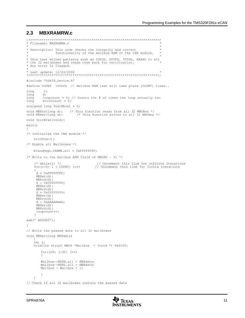
2.3 MBXRAMRW.c/********************************************************************** Filename: MBXRAMRW.c ** ** Description: This code checks the integrity and correct ** functionality of the mailbox RAM in the CAN module. ** ** This test writes patterns such as 0000h, FFFFh, 5555h, AAAAh to all* the 32 mailboxes and reads them back for verification. ** Any error is flagged. * * Last update: 12/24/2002 **********************************************************************/
#include ”DSP28_Device.h”
#define COUNT 100000 // Mailbox RAM test will take place (COUNT) times..
long i;long d;long loopcount = 0; // Counts the # of times the loop actually ranlong errorcount = 0;
unsigned long TestMbox1 = 0;
void MBXrd(long d); /* This function reads from all 32 MBOXes */void MBXwr(long d); /* This function writes to all 32 MBOXes */
void InitECan(void);
main() {
/* Initialize the CAN module */
InitECan();
/* Enable all Mailboxes */
ECanaRegs.CANME.all = 0xFFFFFFFF;
/* Write to the mailbox RAM field of MBOX0 – 31 */ /* while(1) */ // Uncomment this line for infinite iterations for(i=0; i < COUNT; i++) // Uncomment this line for finite iterations { d = 0xFFFFFFFF; MBXwr(d); MBXrd(d); d = 0x00000000; MBXwr(d); MBXrd(d); d = 0x55555555; MBXwr(d); MBXrd(d); d = 0xAAAAAAAA; MBXwr(d); MBXrd(d); loopcount++; }
asm(” ESTOP0”);
}
// Write the passed data to all 32 mailboxes
void MBXwr(long MBXdata) {int j;volatile struct MBOX *Mailbox = (void *) 0x6100;
for(j=0; j<32; j++) {
Mailbox–>MDRH.all = MBXdata;Mailbox–>MDRL.all = MBXdata;Mailbox = Mailbox + 1;
}}
// Check if all 32 mailboxes contain the passed data
Programming Examples for the TMS320F281x eCAN
12 SPRA876A
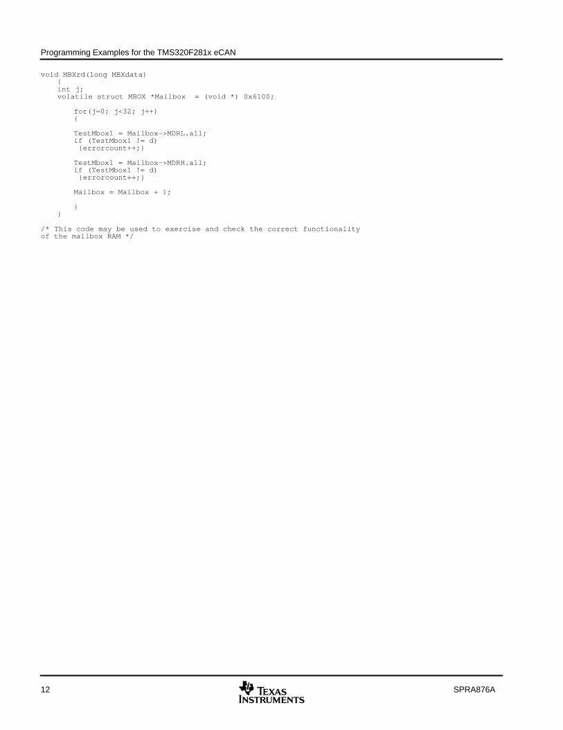
void MBXrd(long MBXdata) {int j;volatile struct MBOX *Mailbox = (void *) 0x6100;
for(j=0; j<32; j++) {
TestMbox1 = Mailbox–>MDRL.all;if (TestMbox1 != d) {errorcount++;} TestMbox1 = Mailbox–>MDRH.all;if (TestMbox1 != d) {errorcount++;} Mailbox = Mailbox + 1;
} }
/* This code may be used to exercise and check the correct functionalityof the mailbox RAM */

Programming Examples for the TMS320F281x eCAN
13SPRA876A
2.4 TXLOOP.c/********************************************************************** Filename: TXLOOP.c ** ** Description: TXLOOP – Transmit loop using any mailbox * * Mailbox 5 is shown as an example...* This program TRANSMITS data to another CAN module using MAILBOX5* This program could either loop forever or transmit ”n” # of times,* where ”n” is the TXCOUNT value.* * Last update: 12/23/2002*********************************************************************/
#include ”DSP28_Device.h”#define TXCOUNT 10000 // Transmission will take place (TXCOUNT) times..
long i;long loopcount = 0;
void InitECan(void);
main(){
/* Create a shadow register structure for the CAN control registers. This is needed, since, only 32–bit access is allowed to these registers. 16–bit access to these registers could potentially corrupt the register contents. This is especially true while writing to a bit (or group of bits) among bits 16 – 31 */
struct ECAN_REGS ECanaShadow;
/* Initialize the CAN module */
InitECan();
/* Write to the MSGID field */ ECanaMboxes.MBOX5.MSGID.all = 0x9FFFFFFF; // Extended Identifier /* Configure Mailbox under test as a Transmit mailbox */
ECanaShadow.CANMD.all = ECanaRegs.CANMD.all;ECanaShadow.CANMD.bit.MD5 = 0;ECanaRegs.CANMD.all = ECanaShadow.CANMD.all;
/* Enable Mailbox under test */
ECanaShadow.CANME.all = ECanaRegs.CANME.all;ECanaShadow.CANME.bit.ME5 = 1;ECanaRegs.CANME.all = ECanaShadow.CANME.all;
/* Write to DLC field in Master Control reg */
ECanaMboxes.MBOX5.MCF.bit.DLC = 8;
/* Write to the mailbox RAM field */ ECanaMboxes.MBOX5.MDRL.all = 0x01234567;
ECanaMboxes.MBOX5.MDRH.all = 0x89ABCDEF;
/* Begin transmitting */
// while(1) // Uncomment this line for infinite transmissions for(i=0; i < TXCOUNT; i++) // Uncomment this line for finite transmissions { ECanaShadow.CANTRS.all = 0; ECanaShadow.CANTRS.bit.TRS5 = 1; // Set TRS for mailbox under test ECanaRegs.CANTRS.all = ECanaShadow.CANTRS.all; while(ECanaRegs.CANTA.bit.TA5 == 0 ) {} // Wait for TA5 bit to be set.. ECanaShadow.CANTA.all = 0; ECanaShadow.CANTA.bit.TA5 = 1; // Clear TA5 ECanaRegs.CANTA.all = ECanaShadow.CANTA.all; loopcount ++; }
}
/* CANalyzer configuration file: 1M80SPRX.cfg... */

Programming Examples for the TMS320F281x eCAN
14 SPRA876A
2.5 RXLOOP.c/********************************************************************** Filename: RXLOOP.c ** ** Description: This test is a simple example of how data may be received * in 28x CAN.** This program runs on Node B. CANalyzer is used as node A in this example.* All mailboxes are configured as receive mailboxes. Each mailbox* has a different ID. All mailboxes in node A are allowed to transmit* in a sequence to mailboxes in node B. Once the cycle is complete,* the cycle is started all over again.
* This program loops forever. The # of times the receive loop is executed* is stored in the RXCOUNT value.* * Last update: 12/24/2002*********************************************************************/
#include ”DSP28_Device.h”
long RXCOUNT = 0;long i;
void InitECan(void);
main() {
/* Create a shadow register structure for the CAN control registers. This is needed, since, only 32–bit access is allowed to these registers. 16–bit access to these registers could potentially corrupt the register contents. This is especially true while writing to a bit (or group of bits) among bits 16 – 31 */
struct ECAN_REGS ECanaShadow;
/* Initialize the CAN module */
InitECan(); /* Write to the MSGID field – MBX number is written as its MSGID */ ECanaMboxes.MBOX1.MSGID.all = 0x00040000; // Std identifier ECanaMboxes.MBOX2.MSGID.all = 0x00080000; // Std identifier ECanaMboxes.MBOX3.MSGID.all = 0x000C0000; // Std identifier ECanaMboxes.MBOX4.MSGID.all = 0x00100000; // Std identifier ECanaMboxes.MBOX5.MSGID.all = 0x00140000; // Std identifier ECanaMboxes.MBOX6.MSGID.all = 0x00180000; // Std identifier ECanaMboxes.MBOX7.MSGID.all = 0x001C0000; // Std identifier ECanaMboxes.MBOX8.MSGID.all = 0x00200000; // Std identifier ECanaMboxes.MBOX9.MSGID.all = 0x00240000; // Std identifier ECanaMboxes.MBOX10.MSGID.all = 0x00400000; // Std identifier ECanaMboxes.MBOX11.MSGID.all = 0x00440000; // Std identifier ECanaMboxes.MBOX12.MSGID.all = 0x00480000; // Std identifier ECanaMboxes.MBOX13.MSGID.all = 0x004C0000; // Std identifier ECanaMboxes.MBOX14.MSGID.all = 0x00500000; // Std identifier ECanaMboxes.MBOX15.MSGID.all = 0x00540000; // Std identifier ECanaMboxes.MBOX16.MSGID.all = 0x00580000; // Std identifier ECanaMboxes.MBOX17.MSGID.all = 0x005C0000; // Std identifier ECanaMboxes.MBOX18.MSGID.all = 0x00600000; // Std identifier ECanaMboxes.MBOX19.MSGID.all = 0x00640000; // Std identifier ECanaMboxes.MBOX20.MSGID.all = 0x00800000; // Std identifier ECanaMboxes.MBOX21.MSGID.all = 0x00840000; // Std identifier ECanaMboxes.MBOX22.MSGID.all = 0x00880000; // Std identifier ECanaMboxes.MBOX23.MSGID.all = 0x008C0000; // Std identifier ECanaMboxes.MBOX24.MSGID.all = 0x00900000; // Std identifier ECanaMboxes.MBOX25.MSGID.all = 0x00940000; // Std identifier ECanaMboxes.MBOX26.MSGID.all = 0x00980000; // Std identifier ECanaMboxes.MBOX27.MSGID.all = 0x009C0000; // Std identifier ECanaMboxes.MBOX28.MSGID.all = 0x00A00000; // Std identifier ECanaMboxes.MBOX29.MSGID.all = 0x00A40000; // Std identifier ECanaMboxes.MBOX30.MSGID.all = 0x00C00000; // Std identifier ECanaMboxes.MBOX31.MSGID.all = 0x00C40000; // Std identifier ECanaMboxes.MBOX0.MSGID.all = 0x00C80000; // Std identifier
/* Note: If writing to only the 11–bit identifier as by”ECanaMboxes.MBOX0.MSGID.bit.MSGID_H = 0x00C8”, IDE, AME & AAMbit fields also need to be initialized. Otherwise, they may assume random values */
/* Configure Mailboxes as Receive mailboxes */

Programming Examples for the TMS320F281x eCAN
15SPRA876A
ECanaShadow.CANMD.all = ECanaRegs.CANMD.all;ECanaShadow.CANMD.all = 0xFFFFFFFF;ECanaRegs.CANMD.all = ECanaShadow.CANMD.all;
/* Enable Mailboxes */
ECanaShadow.CANME.all = ECanaRegs.CANME.all;ECanaShadow.CANME.all = 0xFFFFFFFF;ECanaRegs.CANME.all = ECanaShadow.CANME.all;
/* Begin receiving */
while(1) { while(ECanaRegs.CANRMP.all != 0xFFFFFFFF ) {} // Wait for all RMPn to be set.. ECanaRegs.CANRMP.all = 0xFFFFFFFF; // Clear all RMPn bits and start RXCOUNT++ ; // all over again... }
}
/* CANalyzer configuration file: RXLOOP.CFG... */

Programming Examples for the TMS320F281x eCAN
16 SPRA876A
2.6 TRPRTSTP.c/********************************************************************** Filename: TRPRTSTP.c * * Description: This program illustrates the programmable transmit–priority* and time stamping feature of the CAN module. * * When a priority is assigned, transmission will be according to the* assigned transmit priority, not the numerical value of the mailbox ID.* All mailboxes are configured for transmit operation and all TRS.n bits* are set at the same time. Transmit priority is assigned randomly. * The received data may be monitored on the CANalyzer to check if data was* transmitted according to the assigned priority. The MOTS registers may * also be checked on the transmitting node.** Last update: 12/24/2002*********************************************************************/
#include ”DSP28_Device.h”
long i;
void InitECan(void);
main() {
/* Initialize the CAN module */
InitECan(); /* Write to the MSGID field of TRANSMIT mailboxes MBOX0 – 31 */ ECanaMboxes.MBOX0.MSGID.all = 0x9555AA00; ECanaMboxes.MBOX1.MSGID.all = 0x9555AA01; ECanaMboxes.MBOX2.MSGID.all = 0x9555AA02; ECanaMboxes.MBOX3.MSGID.all = 0x9555AA03; ECanaMboxes.MBOX4.MSGID.all = 0x9555AA04; ECanaMboxes.MBOX5.MSGID.all = 0x9555AA05; ECanaMboxes.MBOX6.MSGID.all = 0x9555AA06; ECanaMboxes.MBOX7.MSGID.all = 0x9555AA07; ECanaMboxes.MBOX8.MSGID.all = 0x9555AA08; ECanaMboxes.MBOX9.MSGID.all = 0x9555AA09; ECanaMboxes.MBOX10.MSGID.all = 0x9555AA10; ECanaMboxes.MBOX11.MSGID.all = 0x9555AA11; ECanaMboxes.MBOX12.MSGID.all = 0x9555AA12; ECanaMboxes.MBOX13.MSGID.all = 0x9555AA13; ECanaMboxes.MBOX14.MSGID.all = 0x9555AA14; ECanaMboxes.MBOX15.MSGID.all = 0x9555AA15; ECanaMboxes.MBOX16.MSGID.all = 0x9555AA16; ECanaMboxes.MBOX17.MSGID.all = 0x9555AA17; ECanaMboxes.MBOX18.MSGID.all = 0x9555AA18; ECanaMboxes.MBOX19.MSGID.all = 0x9555AA19; ECanaMboxes.MBOX20.MSGID.all = 0x9555AA20; ECanaMboxes.MBOX21.MSGID.all = 0x9555AA21; ECanaMboxes.MBOX22.MSGID.all = 0x9555AA22; ECanaMboxes.MBOX23.MSGID.all = 0x9555AA23; ECanaMboxes.MBOX24.MSGID.all = 0x9555AA24; ECanaMboxes.MBOX25.MSGID.all = 0x9555AA25; ECanaMboxes.MBOX26.MSGID.all = 0x9555AA26; ECanaMboxes.MBOX27.MSGID.all = 0x9555AA27; ECanaMboxes.MBOX28.MSGID.all = 0x9555AA28; ECanaMboxes.MBOX29.MSGID.all = 0x9555AA29; ECanaMboxes.MBOX30.MSGID.all = 0x9555AA30; ECanaMboxes.MBOX31.MSGID.all = 0x9555AA31; /* Configure Mailboxes 0–31 as Tx */
ECanaRegs.CANMD.all = 0x00000000;
/* Enable all Mailboxes */
ECanaRegs.CANME.all = 0xFFFFFFFF;
/* Write to Master Control field – DLC */ ECanaMboxes.MBOX0.MCF.bit.DLC = 8; ECanaMboxes.MBOX1.MCF.bit.DLC = 8; ECanaMboxes.MBOX2.MCF.bit.DLC = 8;

Programming Examples for the TMS320F281x eCAN
17SPRA876A
ECanaMboxes.MBOX3.MCF.bit.DLC = 8; ECanaMboxes.MBOX4.MCF.bit.DLC = 8; ECanaMboxes.MBOX5.MCF.bit.DLC = 8; ECanaMboxes.MBOX6.MCF.bit.DLC = 8; ECanaMboxes.MBOX7.MCF.bit.DLC = 8; ECanaMboxes.MBOX8.MCF.bit.DLC = 8; ECanaMboxes.MBOX9.MCF.bit.DLC = 8; ECanaMboxes.MBOX10.MCF.bit.DLC = 8; ECanaMboxes.MBOX11.MCF.bit.DLC = 8; ECanaMboxes.MBOX12.MCF.bit.DLC = 8; ECanaMboxes.MBOX13.MCF.bit.DLC = 8; ECanaMboxes.MBOX14.MCF.bit.DLC = 8; ECanaMboxes.MBOX15.MCF.bit.DLC = 8; ECanaMboxes.MBOX16.MCF.bit.DLC = 8; ECanaMboxes.MBOX17.MCF.bit.DLC = 8; ECanaMboxes.MBOX18.MCF.bit.DLC = 8; ECanaMboxes.MBOX19.MCF.bit.DLC = 8; ECanaMboxes.MBOX20.MCF.bit.DLC = 8; ECanaMboxes.MBOX21.MCF.bit.DLC = 8; ECanaMboxes.MBOX22.MCF.bit.DLC = 8; ECanaMboxes.MBOX23.MCF.bit.DLC = 8; ECanaMboxes.MBOX24.MCF.bit.DLC = 8; ECanaMboxes.MBOX25.MCF.bit.DLC = 8; ECanaMboxes.MBOX26.MCF.bit.DLC = 8; ECanaMboxes.MBOX27.MCF.bit.DLC = 8; ECanaMboxes.MBOX28.MCF.bit.DLC = 8; ECanaMboxes.MBOX29.MCF.bit.DLC = 8; ECanaMboxes.MBOX30.MCF.bit.DLC = 8; ECanaMboxes.MBOX31.MCF.bit.DLC = 8; /* Set transmit priority level – Random priorities are assigned
Uncomment following block to check out the TPL mechanism */ ECanaMboxes.MBOX20.MCF.bit.TPL = 31; ECanaMboxes.MBOX4.MCF.bit.TPL = 30; ECanaMboxes.MBOX9.MCF.bit.TPL = 29; ECanaMboxes.MBOX26.MCF.bit.TPL = 28; ECanaMboxes.MBOX15.MCF.bit.TPL = 27; ECanaMboxes.MBOX0.MCF.bit.TPL = 26; ECanaMboxes.MBOX7.MCF.bit.TPL = 25; ECanaMboxes.MBOX23.MCF.bit.TPL = 24; ECanaMboxes.MBOX11.MCF.bit.TPL = 23; ECanaMboxes.MBOX17.MCF.bit.TPL = 22; ECanaMboxes.MBOX27.MCF.bit.TPL = 21; ECanaMboxes.MBOX13.MCF.bit.TPL = 20; ECanaMboxes.MBOX18.MCF.bit.TPL = 19; ECanaMboxes.MBOX2.MCF.bit.TPL = 18; ECanaMboxes.MBOX24.MCF.bit.TPL = 17; ECanaMboxes.MBOX29.MCF.bit.TPL = 16; ECanaMboxes.MBOX12.MCF.bit.TPL = 15; ECanaMboxes.MBOX16.MCF.bit.TPL = 14; ECanaMboxes.MBOX31.MCF.bit.TPL = 13; ECanaMboxes.MBOX22.MCF.bit.TPL = 12; ECanaMboxes.MBOX19.MCF.bit.TPL = 11; ECanaMboxes.MBOX21.MCF.bit.TPL = 10; ECanaMboxes.MBOX1.MCF.bit.TPL = 9; ECanaMboxes.MBOX30.MCF.bit.TPL = 8; ECanaMboxes.MBOX28.MCF.bit.TPL = 7; ECanaMboxes.MBOX25.MCF.bit.TPL = 6; ECanaMboxes.MBOX10.MCF.bit.TPL = 5; ECanaMboxes.MBOX3.MCF.bit.TPL = 4; ECanaMboxes.MBOX8.MCF.bit.TPL = 3; ECanaMboxes.MBOX5.MCF.bit.TPL = 2; ECanaMboxes.MBOX14.MCF.bit.TPL = 1; ECanaMboxes.MBOX6.MCF.bit.TPL = 0; /* If no tr.priority is assigned, tr.sequence will be starting with the mailbox with the highest priority, which will be the mailbox with the numerically highest ID. 31,30,29.........2,1,0 Uncomment the following block to try this out */ /*ECanaMboxes.MBOX20.MCF.bit.TPL = 0; ECanaMboxes.MBOX4.MCF.bit.TPL = 0; ECanaMboxes.MBOX9.MCF.bit.TPL = 0; ECanaMboxes.MBOX26.MCF.bit.TPL = 0; ECanaMboxes.MBOX15.MCF.bit.TPL = 0; ECanaMboxes.MBOX0.MCF.bit.TPL = 0; ECanaMboxes.MBOX7.MCF.bit.TPL = 0; ECanaMboxes.MBOX23.MCF.bit.TPL = 0;

Programming Examples for the TMS320F281x eCAN
18 SPRA876A
ECanaMboxes.MBOX11.MCF.bit.TPL = 0; ECanaMboxes.MBOX17.MCF.bit.TPL = 0; ECanaMboxes.MBOX27.MCF.bit.TPL = 0; ECanaMboxes.MBOX13.MCF.bit.TPL = 0; ECanaMboxes.MBOX18.MCF.bit.TPL = 0; ECanaMboxes.MBOX2.MCF.bit.TPL = 0; ECanaMboxes.MBOX24.MCF.bit.TPL = 0; ECanaMboxes.MBOX29.MCF.bit.TPL = 0; ECanaMboxes.MBOX12.MCF.bit.TPL = 0; ECanaMboxes.MBOX16.MCF.bit.TPL = 0; ECanaMboxes.MBOX31.MCF.bit.TPL = 0; ECanaMboxes.MBOX22.MCF.bit.TPL = 0; ECanaMboxes.MBOX19.MCF.bit.TPL = 0; ECanaMboxes.MBOX21.MCF.bit.TPL = 0; ECanaMboxes.MBOX1.MCF.bit.TPL = 0; ECanaMboxes.MBOX30.MCF.bit.TPL = 0; ECanaMboxes.MBOX28.MCF.bit.TPL = 0; ECanaMboxes.MBOX25.MCF.bit.TPL = 0; ECanaMboxes.MBOX10.MCF.bit.TPL = 0; ECanaMboxes.MBOX3.MCF.bit.TPL = 0; ECanaMboxes.MBOX8.MCF.bit.TPL = 0; ECanaMboxes.MBOX5.MCF.bit.TPL = 0; ECanaMboxes.MBOX14.MCF.bit.TPL = 0; ECanaMboxes.MBOX6.MCF.bit.TPL = 0; */ /* Write to the mailbox RAM field of MBOX0 – 31 */ ECanaMboxes.MBOX0.MDRL.all = 0x00000000;
ECanaMboxes.MBOX0.MDRH.all = 0x00000000; ECanaMboxes.MBOX1.MDRL.all = 0x00000001; ECanaMboxes.MBOX1.MDRH.all = 0x00000000; ECanaMboxes.MBOX2.MDRL.all = 0x00000002; ECanaMboxes.MBOX2.MDRH.all = 0x00000000; ECanaMboxes.MBOX3.MDRL.all = 0x00000003; ECanaMboxes.MBOX3.MDRH.all = 0x00000000; ECanaMboxes.MBOX4.MDRL.all = 0x00000004; ECanaMboxes.MBOX4.MDRH.all = 0x00000000; ECanaMboxes.MBOX5.MDRL.all = 0x00000005; ECanaMboxes.MBOX5.MDRH.all = 0x00000000; ECanaMboxes.MBOX6.MDRL.all = 0x00000006; ECanaMboxes.MBOX6.MDRH.all = 0x00000000; ECanaMboxes.MBOX7.MDRL.all = 0x00000007; ECanaMboxes.MBOX7.MDRH.all = 0x00000000; ECanaMboxes.MBOX8.MDRL.all = 0x00000008; ECanaMboxes.MBOX8.MDRH.all = 0x00000000; ECanaMboxes.MBOX9.MDRL.all = 0x00000009; ECanaMboxes.MBOX9.MDRH.all = 0x00000000; ECanaMboxes.MBOX10.MDRL.all = 0x00000010; ECanaMboxes.MBOX10.MDRH.all = 0x00000000; ECanaMboxes.MBOX11.MDRL.all = 0x00000011; ECanaMboxes.MBOX11.MDRH.all = 0x00000000; ECanaMboxes.MBOX12.MDRL.all = 0x00000012; ECanaMboxes.MBOX12.MDRH.all = 0x00000000; ECanaMboxes.MBOX13.MDRL.all = 0x00000013; ECanaMboxes.MBOX13.MDRH.all = 0x00000000; ECanaMboxes.MBOX14.MDRL.all = 0x00000014; ECanaMboxes.MBOX14.MDRH.all = 0x00000000; ECanaMboxes.MBOX15.MDRL.all = 0x00000015; ECanaMboxes.MBOX15.MDRH.all = 0x00000000; ECanaMboxes.MBOX16.MDRL.all = 0x00000016; ECanaMboxes.MBOX16.MDRH.all = 0x00000000; ECanaMboxes.MBOX17.MDRL.all = 0x00000017;
Programming Examples for the TMS320F281x eCAN
19SPRA876A
ECanaMboxes.MBOX17.MDRH.all = 0x00000000; ECanaMboxes.MBOX18.MDRL.all = 0x00000018; ECanaMboxes.MBOX18.MDRH.all = 0x00000000; ECanaMboxes.MBOX19.MDRL.all = 0x00000019; ECanaMboxes.MBOX19.MDRH.all = 0x00000000; ECanaMboxes.MBOX20.MDRL.all = 0x00000020; ECanaMboxes.MBOX20.MDRH.all = 0x00000000; ECanaMboxes.MBOX21.MDRL.all = 0x00000021; ECanaMboxes.MBOX21.MDRH.all = 0x00000000; ECanaMboxes.MBOX22.MDRL.all = 0x00000022; ECanaMboxes.MBOX22.MDRH.all = 0x00000000; ECanaMboxes.MBOX23.MDRL.all = 0x00000023; ECanaMboxes.MBOX23.MDRH.all = 0x00000000; ECanaMboxes.MBOX24.MDRL.all = 0x00000024; ECanaMboxes.MBOX24.MDRH.all = 0x00000000; ECanaMboxes.MBOX25.MDRL.all = 0x00000025; ECanaMboxes.MBOX25.MDRH.all = 0x00000000; ECanaMboxes.MBOX26.MDRL.all = 0x00000026; ECanaMboxes.MBOX26.MDRH.all = 0x00000000; ECanaMboxes.MBOX27.MDRL.all = 0x00000027; ECanaMboxes.MBOX27.MDRH.all = 0x00000000; ECanaMboxes.MBOX28.MDRL.all = 0x00000028; ECanaMboxes.MBOX28.MDRH.all = 0x00000000; ECanaMboxes.MBOX29.MDRL.all = 0x00000029; ECanaMboxes.MBOX29.MDRH.all = 0x00000000; ECanaMboxes.MBOX30.MDRL.all = 0x00000030; ECanaMboxes.MBOX30.MDRH.all = 0x00000000; ECanaMboxes.MBOX31.MDRL.all = 0x00000031; ECanaMboxes.MBOX31.MDRH.all = 0x00000000;
ECanaRegs.CANMIM.all = 0xFFFFFFFF;
/* Configure bit timing parameters */
ECanaRegs.CANMC.bit.CCR = 1 ; // Set CCR = 1 while(ECanaRegs.CANES.bit.CCE != 1 ) {} // Wait for CCE bit to be set.. ECanaRegs.CANBTC.bit.BRP = 9; ECanaRegs.CANBTC.bit.TSEG2 = 5; ECanaRegs.CANBTC.bit.TSEG1 = 7; ECanaRegs.CANMC.bit.CCR = 0 ; // Set CCR = 0 while(ECanaRegs.CANES.bit.CCE == !0 ) {} // Wait for CCE bit to be cleared.. /* Begin transmitting */
ECanaRegs.CANTRS.all = 0xFFFFFFFF; // Set TRS for all transmit mailboxes while(ECanaRegs.CANTA.all != 0xFFFFFFFF ) {} // Wait for all TAn bits to be set.. ECanaRegs.CANTA.all = 0xFFFFFFFF; // Clear all TAn
asm(” ESTOP0”); // Stop here after transmission
}
/*
Note 1: If all 32–bits are written to in a register, the registermay be written to without using a shadow register, as illustratedin this code example.
CANalyzer configuration file: 1M80SPRX.cfg... */
Programming Examples for the TMS320F281x eCAN
20 SPRA876A
2.7 DLCTX.c/********************************************************************** Filename: DLCTX.c * * Description: Illustrates the operation of DLC field for a Transmit mailbox. * * Various values of DLC field are tried for mailbox 22* * Last update: 12/24/2002*********************************************************************/
#include ”DSP28_Device.h”
void error(int);
int j; // j is used to store the incrementing DLC values..long i;
void InitECan(void);
main() {
/* Create a shadow register structure for the CAN control registers. This is needed, since, only 32–bit access is allowed to these registers. 16–bit access to these registers could potentially corrupt the register contents. This is especially true while writing to a bit (or group of bits) among bits 16 – 31 */
struct ECAN_REGS ECanaShadow;
/* Initialize the CAN module */
InitECan(); /* Write to the MSGID field */ ECanaMboxes.MBOX22.MSGID.all = 0x80000022; // Ext Identifier (ID = 22) /* Configure Mailbox under test as a Transmit mailbox */
ECanaShadow.CANMD.all = ECanaRegs.CANMD.all;ECanaShadow.CANMD.bit.MD22 = 0;ECanaRegs.CANMD.all = ECanaShadow.CANMD.all;
/* Enable Mailbox under test */
ECanaShadow.CANME.all = ECanaRegs.CANME.all;ECanaShadow.CANME.bit.ME22 = 1;ECanaRegs.CANME.all = ECanaShadow.CANME.all;
/* Write to the mailbox RAM field */ ECanaMboxes.MBOX22.MDRL.all = 0x01234567;
ECanaMboxes.MBOX22.MDRH.all = 0x89ABCDEF;
/* Begin transmitting */
for(j=0; j < 9; j++) // The DLC value is incremented every time
{ // the loop is run ECanaMboxes.MBOX22.MCF.bit.DLC = j; ECanaShadow.CANTRS.all = 0; // Set TRS bit ECanaShadow.CANTRS.bit.TRS22 = 1; ECanaRegs.CANTRS.all = ECanaShadow.CANTRS.all; while(ECanaRegs.CANTA.bit.TA22 == 0 ) {} // Wait for TA22 bit to be set.. ECanaShadow.CANTA.all = 0; // See Note 1 ECanaShadow.CANTA.bit.TA22 = 1; // Clear TA22 ECanaRegs.CANTA.all = ECanaShadow.CANTA.all; asm (” NOP”); } asm(” ESTOP0”);}
void error(int ErrorFlag){ asm(” ESTOP0”); for (;;);}
Programming Examples for the TMS320F281x eCAN
21SPRA876A
/*
Note 1: Initialize the ”shadow–TA register” to zero before setting any bit(s)in order to clear it (them) in the TA register. Otherwise, some other TAn bit(s) that is (are)set could be inadvertently cleared.
Note 2: If DLC values > than 8 are written, those values do get stored inthe DLC field. However, only a DLC value of 8 (and hence 8 bytes) aretransmited on the bus.
A total of nine transmissions progressing from 0 to 8 bytes can be monitoredon the CAN bus.
CANalyzer configuration file: 1M80spRx.cfg*/

Programming Examples for the TMS320F281x eCAN
22 SPRA876A
2.8 DLCRX.c/********************************************************************** Filename: DLCRX.c * * Description: Checks the operation of DLC field for a Receive mailbox. * * DLC for a receive mailbox is irrelevant. The DLC field of the received* frame is copied in the DLC field of the receive mailbox.* Various values of DLC field are tried for mailbox 23. When the transmitting* node transmits various data frames with differing DLC values, the correct* number of bytes can be seen copied in the mailbox RAM window.* * Last update: 12/24/2002*********************************************************************/
#include ”DSP28_Device.h”
#define DLC_val 1 // DLC value attempted to be written into MSGCTRL register// Values 0 thru 8 may be tried..
long i;
void InitECan(void);
main() {
/* Create a shadow register structure for the CAN control registers. This is needed, since, only 32–bit access is allowed to these registers. 16–bit access to these registers could potentially corrupt the register contents. This is especially true while writing to a bit (or group of bits) among bits 16 – 31 */
struct ECAN_REGS ECanaShadow;
/* Initialize the CAN module */
InitECan();
/* Write to the MSGID field */ ECanaMboxes.MBOX23.MSGID.all = 0x008C0000; // Std Identifier (ID = 23) /* Configure Mailbox under test as a Receive mailbox */
ECanaShadow.CANMD.all = ECanaRegs.CANMD.all;ECanaShadow.CANMD.bit.MD23 = 1;ECanaRegs.CANMD.all = ECanaShadow.CANMD.all;
/* Enable Mailbox under test */
ECanaShadow.CANME.all = ECanaRegs.CANME.all;ECanaShadow.CANME.bit.ME23 = 1;ECanaRegs.CANME.all = ECanaShadow.CANME.all;
/* Write to Master Control reg */ // Writes to MCF of a Rcv MBX are irrelevant
ECanaMboxes.MBOX23.MCF.bit.DLC = DLC_val; // Writes to the DLC field of a Rcv MBX // are not carried out
/* Begin Receiving */
while(1) { while(ECanaRegs.CANRMP.bit.RMP23 == 0 ) {} // Wait for RMP23 bit to be set.. ECanaShadow.CANRMP.all = 0; // See Note 1 ECanaShadow.CANRMP.bit.RMP23 = 1; // Clear RMP23 ECanaRegs.CANRMP.all = ECanaShadow.CANRMP.all; asm (” NOP”); } }
/*
Note 1: Initialize the ”shadow–RMP” register to zero before setting any bit(s)in order to clear it (them) in the RMP register. Otherwise, some other RMPn bit(s)that is (are) set could be inadvertently cleared.
Note 2: Data frames with DLC values ranging from 0 – 8 may be transmitted from CANalyzer. Each time, the correct number of bytes will be receivedand the DLC field updated accordingly.
CANalyzer configuration file: DLCRX.cfg*/
Programming Examples for the TMS320F281x eCAN
23SPRA876A
2.9 DBOTX.c/********************************************************************** Filename: DBOTX.c * * Description: Illustrates the operation of DBO field for a Transmit mailbox. * Mailbox 11 is used in this example ** Last update: 12/24/2002*********************************************************************/
#include ”DSP28_Device.h”
void error(int);
long i;
void InitECan(void);
main() {
/* Create a shadow register structure for the CAN control registers. This is needed, since, only 32–bit access is allowed to these registers. 16–bit access to these registers could potentially corrupt the register contents. This is especially true while writing to a bit (or group of bits) among bits 16 – 31 */
struct ECAN_REGS ECanaShadow;
/* Initialize the CAN module */
InitECan();
/* Write to the MSGID field */ ECanaMboxes.MBOX11.MSGID.all = 0x80000011; // Ext Identifier (ID = 11) /* Configure Mailbox under test as a Transmit mailbox */
ECanaShadow.CANMD.all = ECanaRegs.CANMD.all;ECanaShadow.CANMD.bit.MD11 = 0;ECanaRegs.CANMD.all = ECanaShadow.CANMD.all;
/* Enable Mailbox under test */
ECanaShadow.CANME.all = ECanaRegs.CANME.all;ECanaShadow.CANME.bit.ME11 = 1;ECanaRegs.CANME.all = ECanaShadow.CANME.all;
/* Write to Master Control reg */
ECanaMboxes.MBOX11.MCF.bit.DLC = 8;
/* Write to the mailbox RAM field using 16–bit writes */ ECanaMboxes.MBOX11.MDRL.bit.LOW_WORD = 0x0201; ECanaMboxes.MBOX11.MDRL.bit.HI_WORD = 0x0403;
ECanaMboxes.MBOX11.MDRH.bit.LOW_WORD = 0x0605; ECanaMboxes.MBOX11.MDRH.bit.HI_WORD = 0x0807;
/* Configure DBO bit */
ECanaRegs.CANMC.bit.DBO = 1; // See Note 2
/* Begin transmitting */ ECanaShadow.CANTRS.all = 0; // Set TRS bit ECanaShadow.CANTRS.bit.TRS11 = 1; ECanaRegs.CANTRS.all = ECanaShadow.CANTRS.all; while(ECanaRegs.CANTA.bit.TA11 == 0 ) {} // Wait for TA11 bit to be set.. ECanaShadow.CANTA.all = 0; // See Note 1 ECanaShadow.CANTA.bit.TA11 = 1; // Clear TA11 ECanaRegs.CANTA.all = ECanaShadow.CANTA.all; asm(” ESTOP0”); }
/*
Note 1: Initialize the ”shadow–TA register” to zero before setting any bit(s)in order to clear it (them) in the TA register. Otherwise, some other TAn bit(s)that is (are) set could be inadvertently cleared.
Programming Examples for the TMS320F281x eCAN
24 SPRA876A
Note 2: Following is the effect of DBO bit
Let the mailbox RAM contents be as follows...615C: 0201615D: 0403615E: 0605615F: 0807
When DBO = 1, the bytes will be transmitted in the following sequence:01 02 03 04 05 06 07 08
When DBO = 0, the bytes will be transmitted in the following sequence:04 03 02 01 08 07 06 05
CANalyzer configuration file: 1M80spRx.cfg
*/
Programming Examples for the TMS320F281x eCAN
25SPRA876A
2.10 DBORX.c/********************************************************************** Filename: DBORX.c * * Description: Checks the operation of DBO field for a Receive mailbox. * Mailbox 11 is used in this example ** Last update: 12/27/2001*********************************************************************/#include ”DSP28_Device.h”
void infinite_loop();void error(int);
long i;
main() {
/* Create a shadow register structure for the CAN control registers. This is needed, since, only 32–bit access is allowed to these registers. 16–bit access to these registers could potentially corrupt the register contents. This is especially true while writing to a bit (or group of bits) among bits 16 – 31 */
struct ECAN_REGS ECanaShadow;
asm(” EALLOW”);
/* Disable Watchdog */ SysCtrlRegs.WDCR = 0x006F; /* Enable clock to CAN module */ SysCtrlRegs.PCLKCR.all = 0x4000; /* Set PLL multiplication factor */ SysCtrlRegs.PLLCR = 0x000A; // Set PLL to x10 (/2). A CLKIN of 30 MHz would result in // 30 * 10 = 300 (/2) = 150 MHz SYSCLKOUT. for(i=0; i<150000; i++)
{ asm(” NOP”); }
/* Configure CAN pins using GPIO regs*/
GpioMuxRegs.GPFMUX.bit.CANTXA_GPIOF6 = 1;GpioMuxRegs.GPFMUX.bit.CANRXA_GPIOF7 = 1;
/* Configure eCAN RX and TX pins for eCAN transmissions using CAN regs*/ ECanaRegs.CANTIOC.bit.TXFUNC = 1; ECanaRegs.CANRIOC.bit.RXFUNC = 1; /* Disable all Mailboxes */
ECanaRegs.CANME.all = 0;
/* Configure eCAN for HECC mode – (reqd to access mailboxes 16 thru 31) */
ECanaRegs.CANMC.bit.SCM = 1; /* Write to the MSGID field */ ECanaMboxes.MBOX11.MID.all = 0x00440000; // Std Identifier (ID = 11) LAM_REGS.LAM23.bit.LAMI = 1; ECanaLAMRegs.LAM23./* Configure Mailbox under test as a Receive mailbox */
ECanaShadow.CANMD.all = ECanaRegs.CANMD.all;ECanaShadow.CANMD.bit.MD11 = 1;ECanaRegs.CANMD.all = ECanaShadow.CANMD.all;
/* Enable Mailbox under test */
ECanaShadow.CANME.all = ECanaRegs.CANME.all;ECanaShadow.CANME.bit.ME11 = 1;ECanaRegs.CANME.all = ECanaShadow.CANME.all;
/* Configure bit timing parameters */
ECanaRegs.CANMC.bit.CCR = 1 ; // Set CCR = 1
Programming Examples for the TMS320F281x eCAN
26 SPRA876A
while(ECanaRegs.CANES.bit.CCE != 1 ) {} // Wait for CCE bit to be set.. ECanaRegs.CANBTC.bit.BRP = 9; ECanaRegs.CANBTC.bit.TSEG2 = 5; ECanaRegs.CANBTC.bit.TSEG1 = 7; ECanaRegs.CANMC.bit.CCR = 0 ; // Set CCR = 0 while(ECanaRegs.CANES.bit.CCE == !0 ) {} // Wait for CCE bit to be cleared..
/* Configure DBO bit */
ECanaRegs.CANMC.bit.DBO = 1;
/* Begin Receiving */
while(1) { while(ECanaRegs.CANRMP.bit.RMP11 == 0 ) {} // Wait for RMP11 bit to be set.. ECanaShadow.CANRMP.all = 0; // See Note 1 ECanaShadow.CANRMP.bit.RMP11 = 1; // Clear RMP11 ECanaRegs.CANRMP.all = ECanaShadow.CANRMP.all; ECanaRegs.CANMC.bit.DBO = 0; asm (” NOP”); } }
void infinite_loop(){
} void error(int ErrorFlag){ asm(” ESTOP0”); for (;;);}
/* Following are the bit configuration parameters for a 15 MHz CAN clock
BT = 15, TSEG1 = 7, TSEG2 = 5, SP = 60% (TSEG1 + TSEG2 = 12)–––––––1 Mbps : BRP+1 = 10 500 kbps : BRP+1 = 20 250 kbps : BRP+1 = 40 125 kbps : BRP+1 = 80 100 kbps : BRP+1 = 10050 kbps : BRP+1 = 200
BT = 25 i.e. (TSEG1 + TSEG2 = 22) –––––––
TSEG1 = 18, TSEG2 = 4, SP = 80% TSEG1 = 17, TSEG2 = 5, SP = 76% TSEG1 = 16, TSEG2 = 6, SP = 72% TSEG1 = 15, TSEG2 = 7, SP = 68% TSEG1 = 14, TSEG2 = 8, SP = 64%
1 Mbps : BRP+1 = 6 500 kbps : BRP+1 = 12 250 kbps : BRP+1 = 24 125 kbps : BRP+1 = 48 100 kbps : BRP+1 = 6050 kbps : BRP+1 = 120
Note 1: Initialize RMP to zero before setting any bit in order to clear it.Otherwise, some other RMPn bit that is set could be inadvertently cleared
Note 2: Following is the effect of DBO bit
Let CANalyzer transmit the following bytes in the sequence indicated:01 02 03 04 05 06 07 08
When DBO = 1, the mailbox RAM contents be as follows...615C: 0201615D: 0403615E: 0605615F: 0807
When DBO = 0, the mailbox RAM contents be as follows...615C: 0304

Programming Examples for the TMS320F281x eCAN
27SPRA876A
615D: 0102615E: 0708615F: 0506 Use DBORX.cfg from CANalyzer.
*/
Programming Examples for the TMS320F281x eCAN
28 SPRA876A
2.11 MBXWDIF.c/********************************************************************** Filename: MBXWDIF.c * * Description: This code illustrates the functionality of the WDIFn bit.* (WDIF– Write Denied Interrupt Flag)* The identifier field of a mailbox is written to, while it is enabled.* This would set WDIFn bit and assert a CAN interrupt.** Last update: 12/24/2002*********************************************************************/
#include ”DSP28_Device.h”
// Prototype statements for functions found within this file.
interrupt void eCAN0INT_ISR(void);interrupt void eCAN1INT_ISR(void);
// Variable declarations
int int0count = 0; // Counter to track the # of level 0 interruptsint int1count = 0; // Counter to track the # of level 1 interruptslong i;
/* Create a shadow register structure for the CAN control registers. This is needed, since, only 32–bit access is allowed to these registers. 16–bit access to these registers could potentially corrupt the register contents. This is especially true while writing to a bit (or group of bits) among bits 16 – 31 */
struct ECAN_REGS ECanaShadow;
void InitECan(void);
main()
{
/* Initialize the CAN module */
InitECan(); /* Initialize PIE vector table To a Known State: */
// The PIE vector table is initialized with pointers to shell ”Interrupt // Service Routines (ISR)”. The shell routines are found in DSP28_DefaultIsr.c.
// Insert user specific ISR code in the appropriate shell ISR routine in // the DSP28_DefaultIsr.c file. // InitPieVectTable(); // uncomment this line if the shell ISR routines are needed // This function is found in DSP28_PieVect.c. It populates the PIE vector table // with pointers to the shell ISR functions found in DSP28_DefaultIsr.c. This // function is not useful in this code because the user–specific ISR is present // in this file itself. The shell ISR routine in the DSP28_DefaultIsr.c file is // not used. If the shell ISR routines are needed, uncomment this line and add // DSP28_PieVect.c & DSP28_DefaultIsr.c files to the project
/* Disable and clear all CPU interrupts: */
DINT;IER = 0x0000;IFR = 0x0000;
/* Initialize Pie Control Registers To Default State */
InitPieCtrl(); // This function is found in the DSP28_PieCtrl.c file.
/* Write the MSGID prior to enabling (Not strictly required as part of test) */ ECanaMboxes.MBOX13.MSGID.all = 0x9555AA13; /* Write to the mailbox RAM field (Not strictly required as part of test) */ ECanaMboxes.MBOX13.MDRL.all = 0x31313131;
ECanaMboxes.MBOX13.MDRH.all = 0x13131313;
/* Enable Mailbox(es) under test */
ECanaShadow.CANME.all = ECanaRegs.CANME.all;ECanaShadow.CANME.bit.ME13 = 1;ECanaRegs.CANME.all = ECanaShadow.CANME.all;

Programming Examples for the TMS320F281x eCAN
29SPRA876A
/* Configure CAN interrupts */
ECanaShadow.CANGIM.all = ECanaRegs.CANGIM.all; ECanaShadow.CANGIM.bit.WDIM = 1; // Enable ”Write denied” int ECanaShadow.CANGIM.bit.GIL = 0; // GIL value determines eCAN(0/1)INT // Enable the int line chosen by SIL ECanaShadow.CANGIM.bit.I0EN = 1; // Uncomment this line if GIL = 0 //ECanaShadow.CANGIM.bit.I1EN = 1; // Uncomment this line if GIL = 1 ECanaRegs.CANGIM.all = ECanaShadow.CANGIM.all; /* Reassign ISRs. i.e. reassign the PIE vector for ECAN0INTA_ISR and ECAN0INTA_ISR to point to a different ISR than the shell routine found in DSP28_DefaultIsr.c. This is done if the user does not want to use the shell ISR routine but instead wants to embed the ISR in this file itself. */
PieVectTable.ECAN0INTA = &eCAN0INT_ISR;PieVectTable.ECAN1INTA = &eCAN1INT_ISR;
/* Configure PIE interrupts */
PieCtrlRegs.PIECRTL.bit.ENPIE = 1; // Enable vector fetching from PIE block
PieCtrlRegs.PIEACK.bit.ACK9 = 1; // Enables PIE to drive a pulse into the CPU
// The ’Write–denied’ interrupt can be asserted in either of the eCAN interrupt lines// Comment out the unwanted line...
PieCtrlRegs.PIEIER9.bit.INTx5 = 1; // Enable INTx.5 of INT9 (eCAN0INT)PieCtrlRegs.PIEIER9.bit.INTx6 = 0; // Enable INTx.6 of INT9 (eCAN1INT)
/* Configure system interrupts */
IER |= 0x0100; // Enable INT9 of CPUEINT; // Global enable of interrupts
/* Now attempt to write to the MSGID field of the mailboxes */
ECanaMboxes.MBOX13.MSGID.all = 0x9555AA00; asm(” NOP”); // Atleast 8 NOPs are needed asm(” NOP”); // in order for the second write asm(” NOP”); // to assert another interrupt. asm(” NOP”); // Otherwise, the second write asm(” NOP”); // would try to set the ”already set” asm(” NOP”); // WDIF, thereby failing to assert the asm(” NOP”); // second interrupt. asm(” NOP”); ECanaMboxes.MBOX13.MSGID.all = 0x9555AA00; while(1) {} }
/* ––––––––––––––––––––––––––––––––––––––––––––––––––– *//* ISR for PIE INT9.5 *//* Connected to HECC0–INTA eCAN *//* ––––––––––––––––––––––––––––––––––––––––––––––––––––*/
interrupt void eCAN0INT_ISR(void) // eCAN{ // Clear WDIFO flag bit.. ECanaShadow.CANGIF0.all = ECanaRegs.CANGIF0.all; ECanaShadow.CANGIF0.bit.WDIF0 = 1; ECanaRegs.CANGIF0.all = ECanaShadow.CANGIF0.all; int0count++; // Interrupt counter // Re–enable core interrupts and CAN int from PIE module PieCtrlRegs.PIEACK.bit.ACK9 = 1; // Enables PIE to drive a pulse into the CPU IER |= 0x0100; // Enable INT9 EINT; return;}
/* ––––––––––––––––––––––––––––––––––––––––––––––––––– *//* ISR for PIE INT9.6 *//* Connected to HECC1–INTA eCAN *//* ––––––––––––––––––––––––––––––––––––––––––––––––––––*/
interrupt void eCAN1INT_ISR(void) // eCAN{
Programming Examples for the TMS320F281x eCAN
30 SPRA876A
// Clear WDIF1 flag bit.. ECanaShadow.CANGIF1.all = ECanaRegs.CANGIF1.all; ECanaShadow.CANGIF1.bit.WDIF1 = 1; ECanaRegs.CANGIF1.all = ECanaShadow.CANGIF1.all; int1count++; // Interrupt counter // Re–enable core interrupts and CAN int from PIE module PieCtrlRegs.PIEACK.bit.ACK9 = 1; // Enables PIE to drive a pulse into the CPU IER |= 0x0100; // Enable INT9 EINT; return;}
/* When a maskable interrupt request is sent to the CPU the following basic steps are taken by the device: 1. Set the proper IFR bit2. Check if interrupt enabled (Is proper IER bit set?)3. Check if global interrupts enabled (Is INTM cleared?)If both 2 and 3 are true, then proceed as follows:4. Clear IFR5. Store PC, fetch vector, adjust stack, perform context save6. Clear corresponding IER bit (note this register was part of the context save before the bit was cleared)7. Set INTM (mask global interrupts) [note this bit is in ST1 which was part of the context save before it was set]8. Execute interrupt service routine9. Perform context restore (also restores IER and INTM)10.Continue program execution By the time we get to the ISR routine, masked interrupts are disabled (INTM is set)and interrupts from the same vector are also disabled. In this way, no maskableinterrupts will be serviced while we are in the ISR unless we choose to enable them. In this example ISR, the following instructions would be used if nested interrupts areto be allowed:
IER |= 0x0100; // Enable INT9 EINT;
What one might choose to do is only accept interrupts from a differentINT line – so the IER instruction might not be enabling the current interrupt, but insteadallow a different interrupt to come through. Basically in this manner one can do softwareprioritization by allowing some interrupts to be interrupted themselves.
The PIEACK instruction: PieCtrlRegs.PIEACK.bit.ACK9 = 1; // Enables PIE to drive a pulse into the CPU
tells the PIE that you are going to allow interrupts from that group to go on to the CPU(assuming the proper PIER register bit is set). This instruction should be placed in theroutine where you want this to allow this – it might be at the beginning or at the endas the last thing you do before you exit. If you do not do this you will never receiveanother interrupt from that group.
*/
Programming Examples for the TMS320F281x eCAN
31SPRA876A
2.12 TXABORT.c/********************************************************************** Filename: TXABORT.c * * Description: Checks the transmit abort operation using the TRR bit. * * A transmission is initiated for two mailboxes. While the first* mailbox is getting transmitted, the transmission for second mailbox* is aborted. It is then checked whether the AA bit for the second* mailbox is asserted. This test will validate that AAIF bit getting* set in GIF0/GIF1 register is determined by GIL and not MILn bit. * Mailboxes 15 & 29 (with standard identifiers ) are used in this example* * Last update: 12/26/2002*********************************************************************/
#include ”DSP28_Device.h”
// Prototype statements for functions found within this file.
interrupt void eCAN0INT_ISR(void);interrupt void eCAN1INT_ISR(void);
// Variable declarations
long i;int int0count = 0; // Counter to track the # of level 0 interruptsint int1count = 0; // Counter to track the # of level 1 interrupts
void InitECan(void);
/* Create a shadow register structure for the CAN control registers. This is needed, since, only 32–bit access is allowed to these registers. 16–bit access to these registers could potentially corrupt the register contents. This is especially true while writing to a bit (or group of bits) among bits 16 – 31 */
struct ECAN_REGS ECanaShadow;
main()
{
/* Initialize the CAN module */
InitECan(); /* Initialize PIE vector table To a Known State: */
// The PIE vector table is initialized with pointers to shell ”Interrupt // Service Routines (ISR)”. The shell routines are found in DSP28_DefaultIsr.c.
// Insert user specific ISR code in the appropriate shell ISR routine in // the DSP28_DefaultIsr.c file. // InitPieVectTable(); // uncomment this line if the shell ISR routines are needed // This function is found in DSP28_PieVect.c. It populates the PIE vector table // with pointers to the shell ISR functions found in DSP28_DefaultIsr.c. This // function is not useful in this code because the user–specific ISR is present // in this file itself. The shell ISR routine in the DSP28_DefaultIsr.c file is // not used. If the shell ISR routines are needed, uncomment this line and add // DSP28_PieVect.c & DSP28_DefaultIsr.c files to the project
/* Disable and clear all CPU interrupts: */
DINT;IER = 0x0000;IFR = 0x0000;
/* Initialize Pie Control Registers To Default State */
InitPieCtrl(); // This function is found in the DSP28_PieCtrl.c file.
/* Write to the MSGID field */ ECanaMboxes.MBOX15.MSGID.all = 0x00540000; // Std Identifier (ID = 15) ECanaMboxes.MBOX29.MSGID.all = 0x00A40000; // Std Identifier (ID = 29) /* Configure Mailboxes under test as Transmit mailbox */
ECanaShadow.CANMD.all = ECanaRegs.CANMD.all;ECanaShadow.CANMD.bit.MD15 = 0;ECanaShadow.CANMD.bit.MD29 = 0;ECanaRegs.CANMD.all = ECanaShadow.CANMD.all;
Programming Examples for the TMS320F281x eCAN
32 SPRA876A
/* Enable Mailboxes under test */
ECanaShadow.CANME.all = ECanaRegs.CANME.all;ECanaShadow.CANME.bit.ME15 = 1;ECanaShadow.CANME.bit.ME29 = 1;ECanaRegs.CANME.all = ECanaShadow.CANME.all;
/* Write to Master Control reg */
ECanaMboxes.MBOX15.MCF.bit.DLC = 5;ECanaMboxes.MBOX29.MCF.bit.DLC = 5;
/* Write to the mailbox RAM field */ ECanaMboxes.MBOX15.MDRL.all = 0x15151515;
ECanaMboxes.MBOX15.MDRH.all = 0x15151515; ECanaMboxes.MBOX29.MDRL.all = 0x29292929; ECanaMboxes.MBOX29.MDRH.all = 0x29292929;
/* Configure CAN interrupts */
ECanaShadow.CANGIM.all = ECanaRegs.CANGIM.all; ECanaShadow.CANGIM.bit.AAIM = 1; // Enable ”Abort acknowledge” int ECanaShadow.CANGIM.bit.GIL = 0; // GIL value determines eCAN(0/1)INT // Enable the int line chosen by GIL ECanaShadow.CANGIM.bit.I0EN = 1; // Uncomment this line if GIL = 0 //ECanaShadow.CANGIM.bit.I1EN = 1; // Uncomment this line if GIL = 1 ECanaRegs.CANGIM.all = ECanaShadow.CANGIM.all; /* Reassign ISRs. i.e. reassign the PIE vector for ECAN0INTA_ISR and ECAN0INTA_ISR to point to a different ISR than the shell routine found in DSP28_DefaultIsr.c. This is done if the user does not want to use the shell ISR routine but instead wants to embed the ISR in this file itself. */
PieVectTable.ECAN0INTA = &eCAN0INT_ISR;PieVectTable.ECAN1INTA = &eCAN1INT_ISR;
/* Configure PIE interrupts */
PieCtrlRegs.PIECRTL.bit.ENPIE = 1; // Enable vector fetching from PIE block
PieCtrlRegs.PIEACK.bit.ACK9 = 1; // Enables PIE to drive a pulse into the CPU
// The ’TX–Abort’ interrupt can be asserted in either of the eCAN interrupt lines// Comment out the unwanted line...
PieCtrlRegs.PIEIER9.bit.INTx5 = 1; // Enable INTx.5 of INT9 (eCAN0INT)PieCtrlRegs.PIEIER9.bit.INTx6 = 1; // Enable INTx.6 of INT9 (eCAN1INT)
/* Configure system interrupts */
IER |= 0x0100; // Enable INT9 of CPUEINT; // Global enable of interrupts
/* Begin transmitting */
ECanaShadow.CANTRS.all = 0; // Set TRS bit for mailboxes 29 and 15 ECanaShadow.CANTRS.bit.TRS29 = 1; // MBX 29 will be transmitted first, since the ID ECanaShadow.CANTRS.bit.TRS15 = 1; // is numerically higher... ECanaRegs.CANTRS.all = ECanaShadow.CANTRS.all; ECanaShadow.CANTRR.all = 0; // MBX 15 will not be transmitted. ECanaShadow.CANTRR.bit.TRR15 = 1; // Reset mailbox 15 ECanaRegs.CANTRR.all = ECanaShadow.CANTRR.all; while(ECanaRegs.CANTA.bit.TA29 == 0 ) {} // Wait for TA29 bit to be set.. ECanaShadow.CANTA.all = 0; // See Note 1 ECanaShadow.CANTA.bit.TA29 = 1; // Clear TA29 ECanaRegs.CANTA.all = ECanaShadow.CANTA.all; asm(” ESTOP0”);}
/* ––––––––––––––––––––––––––––––––––––––––––––––––––– *//* ISR for PIE INT9.5 *//* Connected to HECC0–INTA eCAN *//* ––––––––––––––––––––––––––––––––––––––––––––––––––––*/
Programming Examples for the TMS320F281x eCAN
33SPRA876A
interrupt void eCAN0INT_ISR(void) // eCAN{ ECanaShadow.CANAA.all = ECanaRegs.CANAA.all ; // Copy AA reg for inspection ECanaShadow.CANGIF0.all = ECanaRegs.CANGIF0.all; // Copy GIF0 reg for inspection ECanaShadow.CANGIF1.all = ECanaRegs.CANGIF1.all; // Copy GIF1 reg for inspection asm (” NOP”); // Useful to set a BP for reg exam
// Clear AA15 and hence AAIF0ECanaShadow.CANAA.all = 0;ECanaShadow.CANAA.bit.AA15 = 1;ECanaRegs.CANAA.all = ECanaShadow.CANAA.all;
// Re–enable core interrupts and CAN int from PIE module PieCtrlRegs.PIEACK.bit.ACK9 = 1; // Enables PIE to drive a pulse into the CPU IER |= 0x0100; // Enable INT9 EINT; int0count++; return;}
/* ––––––––––––––––––––––––––––––––––––––––––––––––––– *//* ISR for PIE INT9.6 *//* Connected to HECC1–INTA eCAN *//* ––––––––––––––––––––––––––––––––––––––––––––––––––––*/
interrupt void eCAN1INT_ISR(void) // eCAN{ ECanaShadow.CANAA.all = ECanaRegs.CANAA.all ; // Copy TOS reg for inspection ECanaShadow.CANGIF0.all = ECanaRegs.CANGIF0.all; // Copy GIF0 reg for inspection ECanaShadow.CANGIF1.all = ECanaRegs.CANGIF1.all; // Copy GIF1 reg for inspection
// Clear AA15 and hence AAIF1ECanaShadow.CANAA.all = 0;ECanaShadow.CANAA.bit.AA15 = 1;ECanaRegs.CANAA.all = ECanaShadow.CANAA.all;
// Re–enable core interrupts and CAN int from PIE module PieCtrlRegs.PIEACK.bit.ACK9 = 1; // Enables PIE to drive a pulse into the CPU IER |= 0x0100; // Enable INT9 EINT; int1count++; return;}
/* Note 1: Initialize the ”shadow–TA register” to zero before setting any bit(s)in order to clear it (them) in the TA register. Otherwise, some other TAn bit(s)that is (are) set could be inadvertently cleared.
Note 2: AAIFn bit in GIFn register is cleared by clearing the set AAn bit.It cannot be cleared by writing a 1 to AAIFn bit.
CANalyzer configuration file: 1M80spRx.cfg*/
Programming Examples for the TMS320F281x eCAN
34 SPRA876A
2.13 RXMSGLST.c/********************************************************************** Filename: RXMSGLST.c * * Description: This test checks the operation OPC bit.* A mailbox is deliberately allowed to be overwritten and it is checked * whether the RMLn and RMLIF bits get set. When the OPC bit is set,* the message should be stored in the next mailbox with a matching identifier.* Mailboxes 21 & 20 is used in this example. ** Last update: 12/24/2002*********************************************************************/
#include ”DSP28_Device.h”
// Prototype statements for functions found within this file.
interrupt void eCAN0INT_ISR(void);interrupt void eCAN1INT_ISR(void);
// Variable declarations
int int0count = 0; // Counter to track the # of level 0 interruptsint int1count = 0; // Counter to track the # of level 1 interruptslong i;void InitECan(void);
/* Create a shadow register structure for the CAN control registers. This is needed, since, only 32–bit access is allowed to these registers. 16–bit access to these registers could potentially corrupt the register contents. This is especially true while writing to a bit (or group of bits) among bits 16 – 31 */
struct ECAN_REGS ECanaShadow;
main()
{
/* Initialize the CAN module */
InitECan(); /* Initialize PIE vector table To a Known State: */
// The PIE vector table is initialized with pointers to shell ”Interrupt // Service Routines (ISR)”. The shell routines are found in DSP28_DefaultIsr.c.
// Insert user specific ISR code in the appropriate shell ISR routine in // the DSP28_DefaultIsr.c file. // InitPieVectTable(); // uncomment this line if the shell ISR routines are needed // This function is found in DSP28_PieVect.c. It populates the PIE vector table // with pointers to the shell ISR functions found in DSP28_DefaultIsr.c. This // function is not useful in this code because the user–specific ISR is present // in this file itself. The shell ISR routine in the DSP28_DefaultIsr.c file is // not used. If the shell ISR routines are needed, uncomment this line and add // DSP28_PieVect.c & DSP28_DefaultIsr.c files to the project
/* Disable and clear all CPU interrupts: */
DINT;IER = 0x0000;IFR = 0x0000;
/* Initialize Pie Control Registers To Default State */
InitPieCtrl(); // This function is found in the DSP28_PieCtrl.c file.
/* Write to the MSGID field */ ECanaMboxes.MBOX21.MSGID.all = 0x00840000; // Std Identifier (ID = 21) ECanaMboxes.MBOX20.MSGID.all = 0x00840000; // Std Identifier (ID = 21) // MBX_LAM–>LAM21.bit.LAMI = 1; /* Enable Mailboxes under test */
ECanaShadow.CANME.all = ECanaRegs.CANME.all;ECanaShadow.CANME.bit.ME21 = 1;ECanaShadow.CANME.bit.ME20 = 1; // Enable only for cases 3 & 4ECanaRegs.CANME.all = ECanaShadow.CANME.all;
/* Initialize the MBX RAM content to a known value */

Programming Examples for the TMS320F281x eCAN
35SPRA876A
ECanaMboxes.MBOX21.MDRH.all = 0;ECanaMboxes.MBOX21.MDRL.all = 0;ECanaMboxes.MBOX20.MDRH.all = 0;ECanaMboxes.MBOX20.MDRL.all = 0;
/* Configure Mailboxes under test as a Receive mailbox */
ECanaShadow.CANMD.all = ECanaRegs.CANMD.all;ECanaShadow.CANMD.bit.MD21 = 1;ECanaShadow.CANMD.bit.MD20 = 1;ECanaRegs.CANMD.all = ECanaShadow.CANMD.all;
/* Configure OPCn bit of the mailbox under test (MBX21) */
ECanaShadow.CANOPC.all = ECanaRegs.CANOPC.all;ECanaShadow.CANOPC.bit.OPC21 = 1; // Set OPC21 = 1 for cases 2 & 4ECanaRegs.CANOPC.all = ECanaShadow.CANOPC.all;
/* Configure CAN interrupts */
ECanaShadow.CANGIM.all = ECanaRegs.CANGIM.all; ECanaShadow.CANGIM.bit.RMLIM = 1; // Enable ”Received message lost” int ECanaShadow.CANGIM.bit.GIL = 0; // GIL value determines eCAN(0/1)INT // Enable the int line chosen by GIL ECanaShadow.CANGIM.bit.I0EN = 1; // Uncomment this line if GIL = 0 ECanaShadow.CANGIM.bit.I1EN = 1; // Uncomment this line if GIL = 1 ECanaRegs.CANGIM.all = ECanaShadow.CANGIM.all; /* Reassign ISRs. i.e. reassign the PIE vector for ECAN0INTA_ISR and ECAN0INTA_ISR to point to a different ISR than the shell routine found in DSP28_DefaultIsr.c. This is done if the user does not want to use the shell ISR routine but instead wants to embed the ISR in this file itself. */
PieVectTable.ECAN0INTA = &eCAN0INT_ISR;PieVectTable.ECAN1INTA = &eCAN1INT_ISR;
/* Configure PIE interrupts */
PieCtrlRegs.PIECRTL.bit.ENPIE = 1; // Enable vector fetching from PIE block
PieCtrlRegs.PIEACK.bit.ACK9 = 1; // Enables PIE to drive a pulse into the CPU
// The ’Received message lost’ interrupt can be asserted in either of the eCAN interrupt lines// Comment out the unwanted line...
PieCtrlRegs.PIEIER9.bit.INTx5 = 1; // Enable INTx.5 of INT9 (eCAN0INT)PieCtrlRegs.PIEIER9.bit.INTx6 = 1; // Enable INTx.6 of INT9 (eCAN1INT)
/* Configure system interrupts */
IER |= 0x0100; // Enable INT9 of CPUEINT; // Global enable of interrupts
/* Begin Receiving */
ECanaRegs.CANRMP.all = 0XFFFFFFFF; // Clear all RMP bits before receiving while(1) {} // Code just loops here while waiting for data...}
/* ––––––––––––––––––––––––––––––––––––––––––––––––––– *//* ISR for PIE INT9.5 *//* Connected to HECC0–INTA eCAN *//* ––––––––––––––––––––––––––––––––––––––––––––––––––––*/
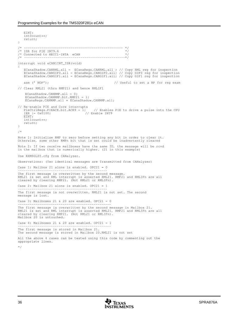
interrupt void eCAN0INT_ISR(void){ ECanaShadow.CANRML.all = ECanaRegs.CANRML.all ; // Copy RML reg for inspection ECanaShadow.CANGIF0.all = ECanaRegs.CANGIF0.all; // Copy GIF0 reg for inspection ECanaShadow.CANGIF1.all = ECanaRegs.CANGIF1.all; // Copy GIF1 reg for inspection asm (” NOP”); // Useful to set a BP for reg exam
// Clear RML21 (thru RMP21) and hence RMLIF0
ECanaShadow.CANRMP.all = 0;ECanaShadow.CANRMP.bit.RMP21 = 1;ECanaRegs.CANRMP.all = ECanaShadow.CANRMP.all;
// Re–enable PIE and Core interrupts PieCtrlRegs.PIEACK.bit.ACK9 = 1; // Enables PIE to drive a pulse into the CPU IER |= 0x0100; // Enable INT9
Programming Examples for the TMS320F281x eCAN
36 SPRA876A
EINT; int0count++; return;}
/* ––––––––––––––––––––––––––––––––––––––––––––––––––– *//* ISR for PIE INT9.6 *//* Connected to HECC1–INTA eCAN *//* ––––––––––––––––––––––––––––––––––––––––––––––––––––*/
interrupt void eCAN1INT_ISR(void){ ECanaShadow.CANRML.all = ECanaRegs.CANRML.all ; // Copy RML reg for inspection ECanaShadow.CANGIF0.all = ECanaRegs.CANGIF0.all; // Copy GIF0 reg for inspection ECanaShadow.CANGIF1.all = ECanaRegs.CANGIF1.all; // Copy GIF1 reg for inspection asm (” NOP”); // Useful to set a BP for reg exam
// Clear RML21 (thru RMP21) and hence RMLIF1
ECanaShadow.CANRMP.all = 0;ECanaShadow.CANRMP.bit.RMP21 = 1;ECanaRegs.CANRMP.all = ECanaShadow.CANRMP.all;
// Re–enable PIE and Core interrupts PieCtrlRegs.PIEACK.bit.ACK9 = 1; // Enables PIE to drive a pulse into the CPU IER |= 0x0100; // Enable INT9 EINT; int1count++; return;}
/*
Note 1: Initialize RMP to zero before setting any bit in order to clear it.Otherwise, some other RMPn bit that is set could be inadvertently cleared
Note 2: If two receive mailboxes have the same ID, the message will be rcvdin the mailbox that is numerically higher. (21 in this example) Use RXMSGLST.cfg from CANalyzer.
Observations: (Two identical messages are Transmitted from CANalyzer)
Case 1: Mailbox 21 alone is enabled. OPC21 = 0––––––––––––––––––––––––––––––––––––––––––––––The first message is overwritten by the second message.RML21 is set and RML interrupt is asserted RML21. RMP21 and RMLIFn are allcleared by clearing RMP21. (Not RML21 or RMLIFn).
Case 2: Mailbox 21 alone is enabled. OPC21 = 1––––––––––––––––––––––––––––––––––––––––––––––The first message is not overwritten. RML21 is not set. The secondmessage is lost.
Case 3: Mailboxes 21 & 20 are enabled. OPC21 = 0––––––––––––––––––––––––––––––––––––––––––––––––The first message is overwritten by the second message in Mailbox 21.RML21 is set and RML interrupt is asserted RML21, RMP21 and RMLIFn are allcleared by clearing RMP21. (Not RML21 or RMLIFn).Mailbox 20 is untouched.
Case 4: Mailboxes 21 & 20 are enabled. OPC21 = 1––––––––––––––––––––––––––––––––––––––––––––––––The first message is stored in Mailbox 21.The second message is stored in Mailbox 20.RML21 is not set
All the above 4 cases can be tested using this code by commenting out theappropriate lines.
*/

Programming Examples for the TMS320F281x eCAN
37SPRA876A
2.14 TCOF.c/********************************************************************** Filename: TCOF.c * * Description: This code checks the functionality of the TCOFn bit.** CAN bit timing registers are configured for 1 Mbps. After a while, the* MSB of the TSC would become 1, which would set TCOFn bit and assert* a CAN interrupt.** Last update: 12/25/2002*********************************************************************/
#include ”DSP28_Device.h”
// Variable declarations
int int0count = 0; // Counter to track the # of level 0 interruptsint int1count = 0; // Counter to track the # of level 1 interruptslong i;void InitECan(void);
// Prototype statements for functions found within this file.
interrupt void eCAN0INT_ISR(void);interrupt void eCAN1INT_ISR(void);
/* Create a shadow register structure for the CAN control registers. This is needed, since, only 32–bit access is allowed to these registers. 16–bit access to these registers could potentially corrupt the register contents. This is especially true while writing to a bit (or group of bits) among bits 16 – 31 */
struct ECAN_REGS ECanaShadow;
main()
{
/* Initialize the CAN module */
InitECan(); /* Initialize PIE vector table To a Known State: */
// The PIE vector table is initialized with pointers to shell ”Interrupt // Service Routines (ISR)”. The shell routines are found in DSP28_DefaultIsr.c.
// Insert user specific ISR code in the appropriate shell ISR routine in // the DSP28_DefaultIsr.c file. // InitPieVectTable(); // uncomment this line if the shell ISR routines are needed // This function is found in DSP28_PieVect.c. It populates the PIE vector table // with pointers to the shell ISR functions found in DSP28_DefaultIsr.c. This // function is not useful in this code because the user–specific ISR is present // in this file itself. The shell ISR routine in the DSP28_DefaultIsr.c file is // not used. If the shell ISR routines are needed, uncomment this line and add // DSP28_PieVect.c & DSP28_DefaultIsr.c files to the project
/* Disable and clear all CPU interrupts: */
DINT;IER = 0x0000;IFR = 0x0000;
/* Initialize Pie Control Registers To Default State */
InitPieCtrl(); // This function is found in the DSP28_PieCtrl.c file.
/* Initialize the Time Stamp Counter (TSC) */
ECanaRegs.CANTSC = 0x7FF00000;
/* Configure CAN interrupts */
ECanaShadow.CANGIM.all = 0; ECanaShadow.CANGIM.bit.TCOM = 1; // Enable ”Timer counter overflow” int ECanaShadow.CANGIM.bit.GIL = 0; // GIL value determines ECAN(0/1)INT ECanaShadow.CANGIM.bit.I0EN = 1; // Enable the int line chosen by GIL ECanaShadow.CANGIM.bit.I1EN = 1; // Enable the int line chosen by GIL ECanaRegs.CANGIM.all = ECanaShadow.CANGIM.all; /* Reassign ISRs. i.e. reassign the PIE vector for ECAN0INTA_ISR and ECAN0INTA_ISR to point to a different ISR than the shell routine found in DSP28_DefaultIsr.c.
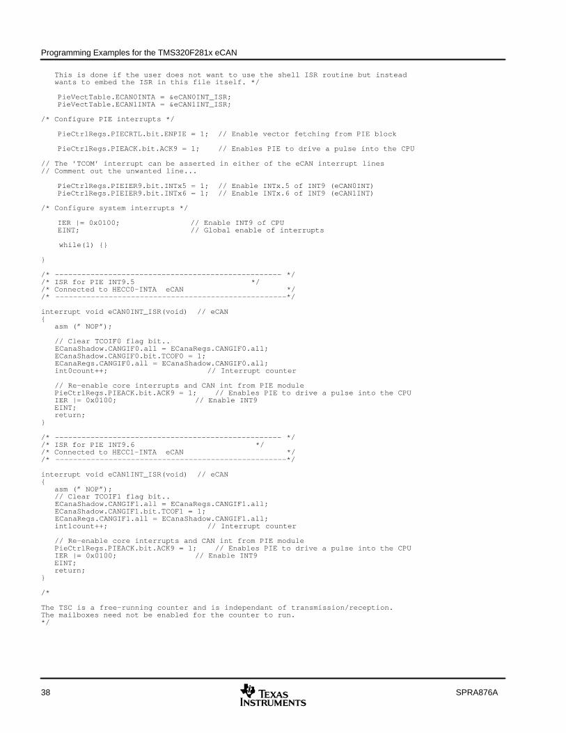
Programming Examples for the TMS320F281x eCAN
38 SPRA876A
This is done if the user does not want to use the shell ISR routine but instead wants to embed the ISR in this file itself. */
PieVectTable.ECAN0INTA = &eCAN0INT_ISR;PieVectTable.ECAN1INTA = &eCAN1INT_ISR;
/* Configure PIE interrupts */
PieCtrlRegs.PIECRTL.bit.ENPIE = 1; // Enable vector fetching from PIE block
PieCtrlRegs.PIEACK.bit.ACK9 = 1; // Enables PIE to drive a pulse into the CPU
// The ’TCOM’ interrupt can be asserted in either of the eCAN interrupt lines// Comment out the unwanted line...
PieCtrlRegs.PIEIER9.bit.INTx5 = 1; // Enable INTx.5 of INT9 (eCAN0INT)PieCtrlRegs.PIEIER9.bit.INTx6 = 1; // Enable INTx.6 of INT9 (eCAN1INT)
/* Configure system interrupts */
IER |= 0x0100; // Enable INT9 of CPUEINT; // Global enable of interrupts
while(1) {} }
/* ––––––––––––––––––––––––––––––––––––––––––––––––––– *//* ISR for PIE INT9.5 *//* Connected to HECC0–INTA eCAN *//* ––––––––––––––––––––––––––––––––––––––––––––––––––––*/
interrupt void eCAN0INT_ISR(void) // eCAN{ asm (” NOP”); // Clear TCOIF0 flag bit.. ECanaShadow.CANGIF0.all = ECanaRegs.CANGIF0.all; ECanaShadow.CANGIF0.bit.TCOF0 = 1; ECanaRegs.CANGIF0.all = ECanaShadow.CANGIF0.all; int0count++; // Interrupt counter // Re–enable core interrupts and CAN int from PIE module PieCtrlRegs.PIEACK.bit.ACK9 = 1; // Enables PIE to drive a pulse into the CPU IER |= 0x0100; // Enable INT9 EINT; return;}
/* ––––––––––––––––––––––––––––––––––––––––––––––––––– *//* ISR for PIE INT9.6 *//* Connected to HECC1–INTA eCAN *//* ––––––––––––––––––––––––––––––––––––––––––––––––––––*/
interrupt void eCAN1INT_ISR(void) // eCAN{ asm (” NOP”); // Clear TCOIF1 flag bit.. ECanaShadow.CANGIF1.all = ECanaRegs.CANGIF1.all; ECanaShadow.CANGIF1.bit.TCOF1 = 1; ECanaRegs.CANGIF1.all = ECanaShadow.CANGIF1.all; int1count++; // Interrupt counter // Re–enable core interrupts and CAN int from PIE module PieCtrlRegs.PIEACK.bit.ACK9 = 1; // Enables PIE to drive a pulse into the CPU IER |= 0x0100; // Enable INT9 EINT; return;}
/*
The TSC is a free–running counter and is independant of transmission/reception.The mailboxes need not be enabled for the counter to run.*/
Programming Examples for the TMS320F281x eCAN
39SPRA876A
2.15 MOTO.c/********************************************************************** Filename: MOTO.c * * Description: This example illustrates the ”MOTO” feature.* * Deliberately let a transmit mailbox timeout and check whether the* corresponding interrupt flag (MTOFn) and TOSn is set.* Mailbox 0 is used in this example** Last update: 12/26/2002*********************************************************************/
#include ”DSP28_Device.h”
// Variable declarations
long i;int int0count = 0; // Counter to track the # of level 0 interruptsint int1count = 0; // Counter to track the # of level 1 interrupts
// Prototype statements for functions found within this file.
interrupt void eCAN0INT_ISR(void);interrupt void eCAN1INT_ISR(void);
/* Create a shadow register structure for the CAN control registers. This is needed, since, only 32–bit access is allowed to these registers. 16–bit access to these registers could potentially corrupt the register contents. This is especially true while writing to a bit (or group of bits) among bits 16 – 31 */
struct ECAN_REGS ECanaShadow;
void InitECan(void);
main()
{
/* Initialize the CAN module */
InitECan();
/* Initialize PIE vector table To a Known State: */// The PIE vector table is initialized with pointers to shell ”Interrupt
// Service Routines (ISR)”. The shell routines are found in DSP28_DefaultIsr.c.// Insert user specific ISR code in the appropriate shell ISR routine in
// the DSP28_DefaultIsr.c file. // InitPieVectTable(); // uncomment this line if the shell ISR routines are needed // This function is found in DSP28_PieVect.c. It populates the PIE vector table // with pointers to the shell ISR functions found in DSP28_DefaultIsr.c. This // function is not useful in this code because the user–specific ISR is present // in this file itself. The shell ISR routine in the DSP28_DefaultIsr.c file is // not used. If the shell ISR routines are needed, uncomment this line and add // DSP28_PieVect.c & DSP28_DefaultIsr.c files to the project
/* Disable and clear all CPU interrupts: */
DINT;IER = 0x0000;IFR = 0x0000;
/* Initialize Pie Control Registers To Default State */
InitPieCtrl(); // This function is found in the DSP28_PieCtrl.c file.
/* Write to the MSGID field */ ECanaMboxes.MBOX0.MSGID.all = 0x9555AA00; /* Configure Mailbox under test as Tx */
ECanaRegs.CANMD.all = 0; // All mailboxes are made transmit..
/* Enable Mailbox under test */
ECanaShadow.CANME.all = ECanaRegs.CANME.all;ECanaShadow.CANME.bit.ME0 = 1;ECanaRegs.CANME.all = ECanaShadow.CANME.all;
/* Write to Master Control field */
Programming Examples for the TMS320F281x eCAN
40 SPRA876A
ECanaMboxes.MBOX0.MCF.bit.DLC = 8; /* Write to the mailbox RAM field */ ECanaMboxes.MBOX0.MDRL.all = 0x9555AAA0;
ECanaMboxes.MBOX0.MDRH.all = 0x89ABCDEF;
/* Configure CAN interrupts */
ECanaShadow.CANMIL.all = ECanaRegs.CANMIL.all;ECanaShadow.CANMIL.bit.MIL0 = 0 ; // MBOX0 asserts MTOF0 (eCAN0INT)//ECanaShadow.CANMIL.bit.MIL0 = 1 ; // MBOX0 asserts MTOF1 (eCAN1INT)ECanaRegs.CANMIL.all = ECanaShadow.CANMIL.all;
ECanaShadow.CANGIM.all = 0; ECanaShadow.CANGIM.bit.I0EN = 1; // Enable eCAN0INT ECanaShadow.CANGIM.bit.I1EN = 1; // Enable eCAN1INT ECanaShadow.CANGIM.bit.MTOM = 1; // Enable MBX Timeout interrupt ECanaRegs.CANGIM.all = ECanaShadow.CANGIM.all; /* Reassign ISRs. i.e. reassign the PIE vector for ECAN0INTA_ISR and ECAN0INTA_ISR to point to a different ISR than the shell routine found in DSP28_DefaultIsr.c. This is done if the user does not want to use the shell ISR routine but instead wants to embed the ISR in this file itself. */
PieVectTable.ECAN0INTA = &eCAN0INT_ISR;PieVectTable.ECAN1INTA = &eCAN1INT_ISR;
/* Configure PIE interrupts */
PieCtrlRegs.PIECRTL.bit.ENPIE = 1; // Enable vector fetching from PIE block
PieCtrlRegs.PIEACK.bit.ACK9 = 1; // Enables PIE to drive a pulse into the CPU
// The ’MOTO’ interrupt can be asserted in either of the eCAN interrupt lines// Comment out the unwanted line...
PieCtrlRegs.PIEIER9.bit.INTx5 = 1; // Enable INTx.5 of INT9 (eCAN0INT)PieCtrlRegs.PIEIER9.bit.INTx6 = 1; // Enable INTx.6 of INT9 (eCAN1INT)
/* Configure system interrupts */
IER |= 0x0100; // Enable INT9 of CPUEINT; // Global enable of interrupts
/* Write to MOTO reg of Mailbox under test */
ECanaMOTORegs.MOTO0 = 0x8D; // It was experimentally determined that // this value would let MBX0 to timeout...MOTS0 contains// 8Eh after transmission is complete..See Note 1
/* Enable time–out function for the mailbox */ ECanaShadow.CANTOC.all = 0;
ECanaShadow.CANTOC.bit.TOC0 = 1;ECanaRegs.CANTOC.all = ECanaShadow.CANTOC.all;
/* Clear the ”Time Stamp Counter” */
ECanaRegs.CANTSC = 0;
/* Begin transmitting */ ECanaShadow.CANTRS.all = 0; ECanaShadow.CANTRS.bit.TRS0 = 1; // Set TRS for mailbox under test ECanaRegs.CANTRS.all = ECanaShadow.CANTRS.all; for(i=0; i<9999999; i++) // A very long loop. Code loops here when CAN module transmits
{ asm(” NOP”); } // the data and executes the ISR asm(” ESTOP0”); // Code stops here after transmission
}
/* ––––––––––––––––––––––––––––––––––––––––––––––––––– *//* ISR for PIE INT9.5 *//* Connected to HECC0–INTA eCAN *//* ––––––––––––––––––––––––––––––––––––––––––––––––––––*/
interrupt void eCAN0INT_ISR(void) // eCAN{
Programming Examples for the TMS320F281x eCAN
41SPRA876A
ECanaShadow.CANTOS.all = ECanaRegs.CANTOS.all ; // Copy TOS reg for inspection ECanaShadow.CANGIF0.all = ECanaRegs.CANGIF0.all; // Copy GIF0 reg for inspection while(ECanaRegs.CANTA.bit.TA0 != 1 ) {} // TAn bit set?
// Clear TAn ECanaShadow.CANTA.all = 0; // Initialize TA to zero before setting any ECanaShadow.CANTA.bit.TA0 = 1 ; // bit in order to clear it. Otherwise, some // other TAn bit that is set could be inadvertently cleared ECanaRegs.CANTA.all = ECanaShadow.CANTA.all ; // Clear TAn bit
// Clear MTOF0 // MTOF0 cannot be manually cleared. It is automatically cleared when TOSn is cleared, // which is automatically cleared when the message is successfully transmitted.
// Re–enable PIE and Core interrupts PieCtrlRegs.PIEACK.bit.ACK9 = 1; // Enables PIE to drive a pulse into the CPU IER |= 0x0100; // These 2 lines allow for nested interrupts EINT; // Strictly not needed for this example. int0count++; return;}
/* ––––––––––––––––––––––––––––––––––––––––––––––––––– *//* ISR for PIE INT9.6 *//* Connected to HECC1–INTA eCAN *//* ––––––––––––––––––––––––––––––––––––––––––––––––––––*/
interrupt void eCAN1INT_ISR(void) // eCAN{ ECanaShadow.CANTOS.all = ECanaRegs.CANTOS.all ; // Copy TOS reg for inspection ECanaShadow.CANGIF1.all = ECanaRegs.CANGIF1.all; // Copy GIF1 reg for inspection while(ECanaRegs.CANTA.bit.TA0 != 1 ) {} // TAn bit set? // Clear TAn ECanaShadow.CANTA.all = 0; // Initialize TA to zero before setting any ECanaShadow.CANTA.bit.TA0 = 1 ; // bit in order to clear it. Otherwise, some // other TAn bit that is set could be inadvertently cleared ECanaRegs.CANTA.all = ECanaShadow.CANTA.all ; // Clear TAn bit
// Clear MTOF1 // MTOF1 cannot be manually cleared. It is automatically cleared when TOSn is cleared, // which is automatically cleared when the message is successfully transmitted. // Re–enable PIE and Core interrupts PieCtrlRegs.PIEACK.bit.ACK9 = 1; // Enables PIE to drive a pulse into the CPU IER |= 0x0100; // Enable INT9 EINT; int1count++; return;}
/* Notes:
The TOS.n bit will be cleared upon (eventual) successful transmission.The only way to ascertain if a time–out occured is to copy TOS and GIFnregisters in the ISR to check if the relevant bits were set when the ISR was just entered.
It can be verified that whether the MTOF bit gets set in GIF0 or GIF1 depends on the value of MILn.
This example is useful to check that MTOFn gets cleared if TOSn is cleared.
Note 1: TSC does not start running until the bit timing registersare configured. After configuration, it is a free running timer clocked by the bit rate clock of the CAN module. The delay between the last instruction that configures the bit timing to the instruction that initiates transmission willtherefore affect this ”experimentally determined” value. Since the counter runs atthe bit clock rate, the fastest bit clock rate is 1 uS, which equates to 150 CPUclock cycles (@ 150 MHz SYSCLKOUT). Therefore adding/deleting a few instructions will not make a significant change. A delay loop would.
*/
Programming Examples for the TMS320F281x eCAN
42 SPRA876A
2.16 LPMWAKEUP.c/********************************************************************** Filename: LPMwakeup.c * * Description: This example illustrates the ability of the CAN module to enter and exit low–power mode (automatically).
The PDR bit of node A is set to force it into low–power mode. The PDA bit is read back to ensure that it is indeed in low–power mode. An attempt is made to write to mailbox 9 RAM while the CAN module is in low–power mode, to ensure that the write fails.. After a while, node B transmits a packet to ”wake–up” node A. The PDA bit is again read back to ensure that node A is indeed out of low–power mode. After wakeup, WUIFn bit must be set as appropriate * Last update: 12/25/2002*********************************************************************/
#include ”DSP28_Device.h”
// Variable declarations
int PDA_STATUS = 0;int int0count = 0; // Counter to track the # of level 0 interruptsint int1count = 0; // Counter to track the # of level 1 interruptslong i;void InitECan(void);
// Prototype statements for functions found within this file.
interrupt void eCAN0INT_ISR(void);interrupt void eCAN1INT_ISR(void);
/* Create a shadow register structure for the CAN control registers. This is needed, since, only 32–bit access is allowed to these registers. 16–bit access to these registers could potentially corrupt the register contents. This is especially true while writing to a bit (or group of bits) among bits 16 – 31 */
struct ECAN_REGS ECanaShadow;
main() {
/* Initialize the CAN module */
InitECan();
/* Initialize PIE vector table To a Known State: */// The PIE vector table is initialized with pointers to shell ”Interrupt
// Service Routines (ISR)”. The shell routines are found in DSP28_DefaultIsr.c.// Insert user specific ISR code in the appropriate shell ISR routine in
// the DSP28_DefaultIsr.c file. // InitPieVectTable(); // uncomment this line if the shell ISR routines are needed // This function is found in DSP28_PieVect.c. It populates the PIE vector table // with pointers to the shell ISR functions found in DSP28_DefaultIsr.c. This // function is not useful in this code because the user–specific ISR is present // in this file itself. The shell ISR routine in the DSP28_DefaultIsr.c file is // not used. If the shell ISR routines are needed, uncomment this line and add // DSP28_PieVect.c & DSP28_DefaultIsr.c files to the project
/* Disable and clear all CPU interrupts: */
DINT;IER = 0x0000;IFR = 0x0000;
/* Initialize Pie Control Registers To Default State */
InitPieCtrl(); // This function is found in the DSP28_PieCtrl.c file. /* Write to the MSGID field */
ECanaMboxes.MBOX0.MSGID.all = 0x9FFFFF00; // MBX0 is a Tx MBX ECanaMboxes.MBOX1.MSGID.all = 0x9FFFFF01; // MBX1 is a Tx MBX ECanaMboxes.MBOX2.MSGID.all = 0x9FFFFF02; // MBX2 is a Tx MBX ECanaMboxes.MBOX3.MSGID.all = 0x9FFFFF03; // MBX3 is a Tx MBX ECanaMboxes.MBOX4.MSGID.all = 0x9FFFFF04; // MBX9 is a Tx MBX ECanaMboxes.MBOX5.MSGID.all = 0x9FFFFF05; // MBX5 is a Tx MBX ECanaMboxes.MBOX6.MSGID.all = 0x9FFFFF06; // MBX6 is a Tx MBX ECanaMboxes.MBOX7.MSGID.all = 0x9FFFFF07; // MBX7 is a Tx MBX
Programming Examples for the TMS320F281x eCAN
43SPRA876A
ECanaMboxes.MBOX8.MSGID.all = 0x9FFFFF08; // MBX8 is the RCV MBX ECanaMboxes.MBOX9.MSGID.all = 0x9FFFFF09; // MBX9 is a Tx MBX
/* Enable Mailboxes under test */
ECanaShadow.CANME.all = 0;ECanaShadow.CANME.bit.ME0 = 1;ECanaShadow.CANME.bit.ME1 = 1;ECanaShadow.CANME.bit.ME2 = 1;ECanaShadow.CANME.bit.ME3 = 1;ECanaShadow.CANME.bit.ME4 = 1;ECanaShadow.CANME.bit.ME5 = 1;ECanaShadow.CANME.bit.ME6 = 1;ECanaShadow.CANME.bit.ME7 = 1;ECanaShadow.CANME.bit.ME8 = 1;ECanaShadow.CANME.bit.ME9 = 1;ECanaRegs.CANME.all = ECanaShadow.CANME.all;
/* Write to the mailbox RAM a known data */
ECanaRegs.CANMD.all = 0x0;ECanaMboxes.MBOX0.MDRH.all = 0x00000000;ECanaMboxes.MBOX0.MDRL.all = 0x00000000;ECanaMboxes.MBOX1.MDRH.all = 0x11111111;ECanaMboxes.MBOX1.MDRL.all = 0x11111111;ECanaMboxes.MBOX2.MDRH.all = 0x22222222;ECanaMboxes.MBOX2.MDRL.all = 0x22222222;ECanaMboxes.MBOX3.MDRH.all = 0x33333333;ECanaMboxes.MBOX3.MDRL.all = 0x33333333;ECanaMboxes.MBOX4.MDRH.all = 0x44444444;ECanaMboxes.MBOX4.MDRL.all = 0x44444444;ECanaMboxes.MBOX5.MDRH.all = 0x55555555;ECanaMboxes.MBOX5.MDRL.all = 0x55555555;ECanaMboxes.MBOX6.MDRH.all = 0x66666666;ECanaMboxes.MBOX6.MDRL.all = 0x66666666;ECanaMboxes.MBOX7.MDRH.all = 0x77777777;ECanaMboxes.MBOX7.MDRL.all = 0x77777777;
ECanaMboxes.MBOX8.MDRH.all = 0x88888888; // MBOX8 = 18181818 after wakeup.ECanaMboxes.MBOX8.MDRL.all = 0x88888888;ECanaMboxes.MBOX9.MDRH.all = 0x99999999;ECanaMboxes.MBOX9.MDRL.all = 0x99999999;
/* Configure Receive mailbox */
ECanaShadow.CANMD.all = 0x0;ECanaShadow.CANMD.bit.MD8 = 1;ECanaRegs.CANMD.all = ECanaShadow.CANMD.all;
/* Write to MCF of Transmit mailboxes */ // Write 00000000 to MCF
ECanaMboxes.MBOX0.MCF.bit.DLC = 8; ECanaMboxes.MBOX1.MCF.bit.DLC = 8; ECanaMboxes.MBOX2.MCF.bit.DLC = 8; ECanaMboxes.MBOX3.MCF.bit.DLC = 8; ECanaMboxes.MBOX4.MCF.bit.DLC = 8; ECanaMboxes.MBOX5.MCF.bit.DLC = 8; ECanaMboxes.MBOX6.MCF.bit.DLC = 8; ECanaMboxes.MBOX7.MCF.bit.DLC = 8; ECanaMboxes.MBOX9.MCF.bit.DLC = 8;
/* Configure CAN interrupts */
ECanaShadow.CANGIM.all = 0; ECanaShadow.CANGIM.bit.WUIM = 1; // Enable ”Wakeup” int ECanaShadow.CANGIM.bit.GIL = 1; // SIL value determines HECC(0/1)INT ECanaShadow.CANGIM.bit.I0EN = 1; // Enable the int line chosen by SIL ECanaShadow.CANGIM.bit.I1EN = 1; // Enable the int line chosen by SIL ECanaRegs.CANGIM.all = ECanaShadow.CANGIM.all; /* Reassign ISRs. i.e. reassign the PIE vector for ECAN0INTA_ISR and ECAN0INTA_ISR to point to a different ISR than the shell routine found in DSP28_DefaultIsr.c. This is done if the user does not want to use the shell ISR routine but instead wants to embed the ISR in this file itself. */
PieVectTable.ECAN0INTA = &eCAN0INT_ISR;PieVectTable.ECAN1INTA = &eCAN1INT_ISR;
/* Configure PIE interrupts */
PieCtrlRegs.PIECRTL.bit.ENPIE = 1; // Enable vector fetching from PIE block
Programming Examples for the TMS320F281x eCAN
44 SPRA876A
PieCtrlRegs.PIEACK.bit.ACK9 = 1; // Enables PIE to drive a pulse into the CPU
// The ’Wakeup’ interrupt can be asserted in either of the eCAN interrupt lines// Comment out the unwanted line...
PieCtrlRegs.PIEIER9.bit.INTx5 = 1; // Enable INTx.5 of INT9 (eCAN0INT)PieCtrlRegs.PIEIER9.bit.INTx6 = 1; // Enable INTx.6 of INT9 (eCAN1INT)
/* Configure system interrupts */
IER |= 0x0100; // Enable INT9 of CPUEINT; // Global enable of interrupts
/* Configure WUBA */
ECanaRegs.CANMC.bit.WUBA = 1; // Set WUBA = 1 so that node can ”wakeup” ECanaShadow.CANTRS.all = 0x000002FF; ECanaRegs.CANTRS.all = ECanaShadow.CANTRS.all; // Initiate a transmit for // all Tx mailboxes while(ECanaRegs.CANTRS.all !=0) {} // Loop here until all mailboxes are // transmitted /* Drive the CAN module into low power mode by setting the PDR bit */ ECanaRegs.CANMC.bit.PDR = 1 ; // Set PDR = 1
while (ECanaRegs.CANES.bit.PDA != 1) {} // Loop here if PDA != 1PDA_STATUS = ECanaRegs.CANES.bit.PDA;
/* Attempt to write to MBX9 RAM to verify if LPM has indeed been entered */
ECanaMboxes.MBOX9.MDRH.all = 0x01234567; // This data should not beECanaMboxes.MBOX9.MDRL.all = 0x89ABCDEF; // written into the MBX RAM
while(ECanaRegs.CANRMP.bit.RMP8 ==0 ) {} // Wait for data to wakeup... /* Now node B transmits the same data twice; the first data ”wakes up”the 28x , the second data is stored in MBX8. It is verfied whether the second data is received and stored in MBX8 */
/* Read PDA bit to make sure it is 0 */
PDA_STATUS = ECanaRegs.CANES.bit.PDA;
asm (” ESTOP0”);
}
/* ––––––––––––––––––––––––––––––––––––––––––––––––––– *//* ISR for PIE INT9.5 *//* Connected to HECC0–INTA eCAN *//* ––––––––––––––––––––––––––––––––––––––––––––––––––––*/
interrupt void eCAN0INT_ISR(void) // eCAN{ ECanaShadow.CANTA.all = 0x000002FF; // Clear WUIF0 flag bit.. ECanaShadow.CANGIF0.all = ECanaRegs.CANGIF0.all; ECanaShadow.CANGIF0.bit.WUIF0 = 1; ECanaRegs.CANGIF0.all = ECanaShadow.CANGIF0.all; int0count++; // Interrupt counter // Re–enable core interrupts and CAN int from PIE module PieCtrlRegs.PIEACK.bit.ACK9 = 1; // Enables PIE to drive a pulse into the CPU IER |= 0x0100; // Enable INT9 EINT; return;}
/* ––––––––––––––––––––––––––––––––––––––––––––––––––– *//* ISR for PIE INT9.6 *//* Connected to HECC1–INTA eCAN *//* ––––––––––––––––––––––––––––––––––––––––––––––––––––*/
interrupt void eCAN1INT_ISR(void) // eCAN{ ECanaShadow.CANTA.all = 0x000002FF; // Clear WUIF1 flag bit.. ECanaShadow.CANGIF1.all = ECanaRegs.CANGIF1.all;
Programming Examples for the TMS320F281x eCAN
45SPRA876A
ECanaShadow.CANGIF1.bit.WUIF1 = 1; ECanaRegs.CANGIF1.all = ECanaShadow.CANGIF1.all; int1count++; // Interrupt counter // Re–enable core interrupts and CAN int from PIE module PieCtrlRegs.PIEACK.bit.ACK9 = 1; // Enables PIE to drive a pulse into the CPU IER |= 0x0100; // Enable INT9 EINT; return;}
/*
OBSERVATIONS:
The following can be observed while executing this example:> 1. Setting PDR = 1, puts the module in LPM> 2. Write to mailbox RAM fails when CAN is in LPM.> 3. CAN module wakes up, when node B transmits a frame twice. The first> frame wakes up the CAN. The second frame is correctly received by the> configured mailbox. The first dataframe may generate an error frame if,> there are only 2 nodes in the network (28x and CANalyzer, for example).> Apart from CANalyzer, the only other node is in LPM and there is no node to> generate an ACK for the frame CANalyzer transmits to wakeup.> 4. The WUBA bit works as intended.> 5. The WUIFn bit is correctly set upon wakeup.> 6. The CAN module exits LPM when PDR bit is cleared to zero.
> Atleast 80 NOPs are needed after the statement that sets the > TRS bit before the statement that sets the PDR bit =1. Only then is the> data in mailbox RAM is transmitted BEFORE the CAN module goes into LPM mode> Otherwise, the data is transmitted AFTER the CAN module wakes up.> To ensure all mailboxes have transmitted before putting the CAN module in > LPM, the CANTRS register may be checked.
CANalyzer configuration file: LPMWAKE.cfg*/
Programming Examples for the TMS320F281x eCAN
46 SPRA876A
2.17 REMREQ2.c/********************************************************************** Filename: REMREQ2.c
Description: This test checks the ability of the CAN module to SEND remote frames from (and receive dataframes in) the SAME Mailbox.
Mailboxes 2,3,4,5 in 28x are configured as Receive mailboxes and theirTRS bits and RTR bits are set. This enables the same mailbox to transmita remote frame and receive the corresponding data frame. Mailboxes in node B (a LF2407A EVM) would transmit DATA frames to the four Rxmailboxes in 28x, matching the ID of mailboxes. (ECN Ref #15)
* Last update: 12/25/2002*********************************************************************/
#include ”DSP28_Device.h”
long i;long loopcount = 0;void InitECan(void);
main() {
/* Create a shadow register structure for the CAN control registers. This is needed, since, only 32–bit access is allowed to these registers. 16–bit access to these registers could potentially corrupt the register contents. This is especially true while writing to a bit (or group of bits) among bits 16 – 31 */
struct ECAN_REGS ECanaShadow;
/* Initialize the CAN module */
InitECan();
/* Initialize mailbox data to zero */
ECanaMboxes.MBOX2.MDRH.all = 0x00000000;ECanaMboxes.MBOX2.MDRL.all = 0x00000000;ECanaMboxes.MBOX3.MDRH.all = 0x00000000;ECanaMboxes.MBOX3.MDRL.all = 0x00000000;ECanaMboxes.MBOX4.MDRH.all = 0x00000000;ECanaMboxes.MBOX4.MDRL.all = 0x00000000;ECanaMboxes.MBOX5.MDRH.all = 0x00000000;ECanaMboxes.MBOX5.MDRL.all = 0x00000000;
/* Write to the MSGID field */ ECanaMboxes.MBOX2.MSGID.all = 0x8AAAAA02; // Ext identifier ECanaMboxes.MBOX3.MSGID.all = 0x8AAAAA03; // Ext identifier ECanaMboxes.MBOX4.MSGID.all = 0x8AAAAA04; // Ext identifier ECanaMboxes.MBOX5.MSGID.all = 0x8AAAAA05; // Ext identifier /* Enable all Mailboxes */
ECanaRegs.CANME.all = 0x0000003C;
/* Write to Master Control field – RTR */ ECanaMboxes.MBOX2.MCF.bit.RTR = 1; ECanaMboxes.MBOX3.MCF.bit.RTR = 1; ECanaMboxes.MBOX4.MCF.bit.RTR = 1; ECanaMboxes.MBOX5.MCF.bit.RTR = 1; ECanaMboxes.MBOX2.MCF.bit.DLC = 8; ECanaMboxes.MBOX3.MCF.bit.DLC = 8; ECanaMboxes.MBOX4.MCF.bit.DLC = 8; ECanaMboxes.MBOX5.MCF.bit.DLC = 7; /* Configure all Mailboxes as Rx */
ECanaRegs.CANMD.all = 0x0000003C; /* Transmit the remote frames and Wait for data frames.. */
ECanaShadow.CANTRS.all = 0; ECanaShadow.CANTRS.all = 0x0000003C; // Set TRS for Rx mailboxes ECanaRegs.CANTRS.all = ECanaShadow.CANTRS.all;
while(1) {}

Programming Examples for the TMS320F281x eCAN
47SPRA876A
}
/*
Observations:
28x sent remote frames from mailboxes 2,3,4,5 to mailboxes 2,3,4,5 ina 2407 EVM. The corresponding data frames were received in mailboxes 2,3,4,5 of 28x.
It is important to correctly configure the DLC value in the remote framesince only that many bytes will be transmitted in the data frame.
Use 1M80spRX.CFG in CANalyzer.
Use REM28ANS.asm in the 2407 EVM*/
Programming Examples for the TMS320F281x eCAN
48 SPRA876A
2.18 REMANS.c/********************************************************************** Filename: REMANS.c * Description: This test checks the ability of the CAN module to answer remote frames automatically.
All mailboxes in 28x are configured as transmit mailboxes with the AAMbit set. Each mailbox has a different ID. Mailboxes in node B (CANalyzer)would transmit remote frames to all the 32 mailboxes in 28x, matching theID of mailboxes. The data frames will be received in mailboxes of node B.This example verifies that RFPn bit is not set if AAM bit is not set.
* Last update: 12/26/2002*********************************************************************/
#include ”DSP28_Device.h”#define TXCOUNT 100000 // Transmission will take place (TXCOUNT) times..
long i;long loopcount = 0;
void infinite_loop();void error(int);void InitECan(void);
main() {
/* Create a shadow register structure for the CAN control registers. This is needed, since, only 32–bit access is allowed to these registers. 16–bit access to these registers could potentially corrupt the register contents. This is especially true while writing to a bit (or group of bits) among bits 16 – 31 */
struct ECAN_REGS ECanaShadow;
/* Initialize the CAN module */
InitECan(); /* Write to the MSGID field ––> AAM bit = 1 */ ECanaMboxes.MBOX1.MSGID.all = 0x20040000; // Std identifier ECanaMboxes.MBOX2.MSGID.all = 0x20080000; // Std identifier ECanaMboxes.MBOX3.MSGID.all = 0x200C0000; // Std identifier ECanaMboxes.MBOX4.MSGID.all = 0x20100000; // Std identifier ECanaMboxes.MBOX5.MSGID.all = 0x20140000; // Std identifier ECanaMboxes.MBOX6.MSGID.all = 0x20180000; // Std identifier ECanaMboxes.MBOX7.MSGID.all = 0x201C0000; // Std identifier ECanaMboxes.MBOX8.MSGID.all = 0x20200000; // Std identifier ECanaMboxes.MBOX9.MSGID.all = 0x20240000; // Std identifier ECanaMboxes.MBOX10.MSGID.all = 0x20400000; // Std identifier ECanaMboxes.MBOX11.MSGID.all = 0x20440000; // Std identifier ECanaMboxes.MBOX12.MSGID.all = 0x20480000; // Std identifier ECanaMboxes.MBOX13.MSGID.all = 0x204C0000; // Std identifier ECanaMboxes.MBOX14.MSGID.all = 0x20500000; // Std identifier ECanaMboxes.MBOX15.MSGID.all = 0x20540000; // Std identifier ECanaMboxes.MBOX16.MSGID.all = 0x20580000; // Std identifier ECanaMboxes.MBOX17.MSGID.all = 0x205C0000; // Std identifier ECanaMboxes.MBOX18.MSGID.all = 0x20600000; // Std identifier ECanaMboxes.MBOX19.MSGID.all = 0x20640000; // Std identifier ECanaMboxes.MBOX20.MSGID.all = 0x20800000; // Std identifier ECanaMboxes.MBOX21.MSGID.all = 0x20840000; // Std identifier ECanaMboxes.MBOX22.MSGID.all = 0x20880000; // Std identifier ECanaMboxes.MBOX23.MSGID.all = 0x208C0000; // Std identifier ECanaMboxes.MBOX24.MSGID.all = 0x20900000; // Std identifier ECanaMboxes.MBOX25.MSGID.all = 0x20940000; // Std identifier ECanaMboxes.MBOX26.MSGID.all = 0x20980000; // Std identifier ECanaMboxes.MBOX27.MSGID.all = 0x209C0000; // Std identifier ECanaMboxes.MBOX28.MSGID.all = 0x20A00000; // Std identifier ECanaMboxes.MBOX29.MSGID.all = 0x20A40000; // Std identifier ECanaMboxes.MBOX30.MSGID.all = 0x20C00000; // Std identifier ECanaMboxes.MBOX31.MSGID.all = 0x20C40000; // Std identifier ECanaMboxes.MBOX0.MSGID.all = 0x20C80000; // Std identifier /* This block turns off AAM ––> AAM =0 */ /* ECanaMboxes.MBOX0.MSGID.bit.AAM = 0; ECanaMboxes.MBOX1.MSGID.bit.AAM = 0; ECanaMboxes.MBOX2.MSGID.bit.AAM = 0; ECanaMboxes.MBOX3.MSGID.bit.AAM = 0;
Programming Examples for the TMS320F281x eCAN
49SPRA876A
ECanaMboxes.MBOX4.MSGID.bit.AAM = 0; ECanaMboxes.MBOX5.MSGID.bit.AAM = 0; ECanaMboxes.MBOX6.MSGID.bit.AAM = 0; ECanaMboxes.MBOX7.MSGID.bit.AAM = 0; ECanaMboxes.MBOX7.MSGID.bit.AAM = 0; ECanaMboxes.MBOX8.MSGID.bit.AAM = 0; ECanaMboxes.MBOX9.MSGID.bit.AAM = 0; ECanaMboxes.MBOX10.MSGID.bit.AAM = 0; ECanaMboxes.MBOX11.MSGID.bit.AAM = 0; ECanaMboxes.MBOX12.MSGID.bit.AAM = 0; ECanaMboxes.MBOX13.MSGID.bit.AAM = 0; ECanaMboxes.MBOX14.MSGID.bit.AAM = 0; ECanaMboxes.MBOX15.MSGID.bit.AAM = 0; ECanaMboxes.MBOX16.MSGID.bit.AAM = 0; ECanaMboxes.MBOX17.MSGID.bit.AAM = 0; ECanaMboxes.MBOX18.MSGID.bit.AAM = 0; ECanaMboxes.MBOX19.MSGID.bit.AAM = 0; ECanaMboxes.MBOX20.MSGID.bit.AAM = 0; ECanaMboxes.MBOX21.MSGID.bit.AAM = 0; ECanaMboxes.MBOX22.MSGID.bit.AAM = 0; ECanaMboxes.MBOX23.MSGID.bit.AAM = 0; ECanaMboxes.MBOX24.MSGID.bit.AAM = 0; ECanaMboxes.MBOX25.MSGID.bit.AAM = 0; ECanaMboxes.MBOX26.MSGID.bit.AAM = 0; ECanaMboxes.MBOX27.MSGID.bit.AAM = 0; ECanaMboxes.MBOX28.MSGID.bit.AAM = 0; ECanaMboxes.MBOX29.MSGID.bit.AAM = 0; ECanaMboxes.MBOX30.MSGID.bit.AAM = 0; ECanaMboxes.MBOX31.MSGID.bit.AAM = 0; */ /* Configure Mailboxes 0–31 as Tx */
ECanaRegs.CANMD.all = 0x00000000;
/* Enable all Mailboxes */
ECanaRegs.CANME.all = 0xFFFFFFFF;
/* Write to Master Control field – DLC */ ECanaMboxes.MBOX0.MCF.bit.DLC = 8; ECanaMboxes.MBOX1.MCF.bit.DLC = 8; ECanaMboxes.MBOX2.MCF.bit.DLC = 8; ECanaMboxes.MBOX3.MCF.bit.DLC = 8; ECanaMboxes.MBOX4.MCF.bit.DLC = 8; ECanaMboxes.MBOX5.MCF.bit.DLC = 8; ECanaMboxes.MBOX6.MCF.bit.DLC = 8; ECanaMboxes.MBOX7.MCF.bit.DLC = 8; ECanaMboxes.MBOX8.MCF.bit.DLC = 8; ECanaMboxes.MBOX9.MCF.bit.DLC = 8; ECanaMboxes.MBOX10.MCF.bit.DLC = 8; ECanaMboxes.MBOX11.MCF.bit.DLC = 8; ECanaMboxes.MBOX12.MCF.bit.DLC = 8; ECanaMboxes.MBOX13.MCF.bit.DLC = 8; ECanaMboxes.MBOX14.MCF.bit.DLC = 8; ECanaMboxes.MBOX15.MCF.bit.DLC = 8; ECanaMboxes.MBOX16.MCF.bit.DLC = 8; ECanaMboxes.MBOX17.MCF.bit.DLC = 8; ECanaMboxes.MBOX18.MCF.bit.DLC = 8; ECanaMboxes.MBOX19.MCF.bit.DLC = 8; ECanaMboxes.MBOX20.MCF.bit.DLC = 8; ECanaMboxes.MBOX21.MCF.bit.DLC = 8; ECanaMboxes.MBOX22.MCF.bit.DLC = 8; ECanaMboxes.MBOX23.MCF.bit.DLC = 8; ECanaMboxes.MBOX24.MCF.bit.DLC = 8; ECanaMboxes.MBOX25.MCF.bit.DLC = 8; ECanaMboxes.MBOX26.MCF.bit.DLC = 8; ECanaMboxes.MBOX27.MCF.bit.DLC = 8; ECanaMboxes.MBOX28.MCF.bit.DLC = 8; ECanaMboxes.MBOX29.MCF.bit.DLC = 8; ECanaMboxes.MBOX30.MCF.bit.DLC = 8; ECanaMboxes.MBOX31.MCF.bit.DLC = 8; /* Write to the mailbox RAM field of MBOX0 – 31 */ ECanaMboxes.MBOX0.MDRL.all = 0x9555AAA0;
ECanaMboxes.MBOX0.MDRH.all = 0x89ABCDEF; ECanaMboxes.MBOX1.MDRL.all = 0x9555AAA1;

Programming Examples for the TMS320F281x eCAN
50 SPRA876A
ECanaMboxes.MBOX1.MDRH.all = 0x89ABCDEF; ECanaMboxes.MBOX2.MDRL.all = 0x9555AAA2; ECanaMboxes.MBOX2.MDRH.all = 0x89ABCDEF; ECanaMboxes.MBOX3.MDRL.all = 0x9555AAA3; ECanaMboxes.MBOX3.MDRH.all = 0x89ABCDEF; ECanaMboxes.MBOX4.MDRL.all = 0x9555AAA4; ECanaMboxes.MBOX4.MDRH.all = 0x89ABCDEF; ECanaMboxes.MBOX5.MDRL.all = 0x9555AAA5; ECanaMboxes.MBOX5.MDRH.all = 0x89ABCDEF; ECanaMboxes.MBOX6.MDRL.all = 0x9555AAA6; ECanaMboxes.MBOX6.MDRH.all = 0x89ABCDEF; ECanaMboxes.MBOX7.MDRL.all = 0x9555AAA7; ECanaMboxes.MBOX7.MDRH.all = 0x89ABCDEF; ECanaMboxes.MBOX8.MDRL.all = 0x9555AAA8; ECanaMboxes.MBOX8.MDRH.all = 0x89ABCDEF; ECanaMboxes.MBOX9.MDRL.all = 0x9555AAA9; ECanaMboxes.MBOX9.MDRH.all = 0x89ABCDEF; ECanaMboxes.MBOX10.MDRL.all = 0x9555AAAA; ECanaMboxes.MBOX10.MDRH.all = 0x89ABCDEF; ECanaMboxes.MBOX11.MDRL.all = 0x9555AAAB; ECanaMboxes.MBOX11.MDRH.all = 0x89ABCDEF; ECanaMboxes.MBOX12.MDRL.all = 0x9555AAAC; ECanaMboxes.MBOX12.MDRH.all = 0x89ABCDEF; ECanaMboxes.MBOX13.MDRL.all = 0x9555AAAD; ECanaMboxes.MBOX13.MDRH.all = 0x89ABCDEF; ECanaMboxes.MBOX14.MDRL.all = 0x9555AAAE; ECanaMboxes.MBOX14.MDRH.all = 0x89ABCDEF; ECanaMboxes.MBOX15.MDRL.all = 0x9555AAAF; ECanaMboxes.MBOX15.MDRH.all = 0x89ABCDEF; ECanaMboxes.MBOX16.MDRL.all = 0x9555AA10; ECanaMboxes.MBOX16.MDRH.all = 0x89ABCDEF; ECanaMboxes.MBOX17.MDRL.all = 0x9555AA11; ECanaMboxes.MBOX17.MDRH.all = 0x89ABCDEF; ECanaMboxes.MBOX18.MDRL.all = 0x9555AA12; ECanaMboxes.MBOX18.MDRH.all = 0x89ABCDEF; ECanaMboxes.MBOX19.MDRL.all = 0x9555AA13; ECanaMboxes.MBOX19.MDRH.all = 0x89ABCDEF; ECanaMboxes.MBOX20.MDRL.all = 0x9555AA14; ECanaMboxes.MBOX20.MDRH.all = 0x89ABCDEF; ECanaMboxes.MBOX21.MDRL.all = 0x9555AA15; ECanaMboxes.MBOX21.MDRH.all = 0x89ABCDEF; ECanaMboxes.MBOX22.MDRL.all = 0x9555AA16; ECanaMboxes.MBOX22.MDRH.all = 0x89ABCDEF; ECanaMboxes.MBOX23.MDRL.all = 0x9555AA17; ECanaMboxes.MBOX23.MDRH.all = 0x89ABCDEF; ECanaMboxes.MBOX24.MDRL.all = 0x9555AA18; ECanaMboxes.MBOX24.MDRH.all = 0x89ABCDEF; ECanaMboxes.MBOX25.MDRL.all = 0x9555AA19; ECanaMboxes.MBOX25.MDRH.all = 0x89ABCDEF; ECanaMboxes.MBOX26.MDRL.all = 0x9555AA1A; ECanaMboxes.MBOX26.MDRH.all = 0x89ABCDEF; ECanaMboxes.MBOX27.MDRL.all = 0x9555AA1B; ECanaMboxes.MBOX27.MDRH.all = 0x89ABCDEF;

Programming Examples for the TMS320F281x eCAN
51SPRA876A
ECanaMboxes.MBOX28.MDRL.all = 0x9555AA1C; ECanaMboxes.MBOX28.MDRH.all = 0x89ABCDEF; ECanaMboxes.MBOX29.MDRL.all = 0x9555AA1D; ECanaMboxes.MBOX29.MDRH.all = 0x89ABCDEF; ECanaMboxes.MBOX30.MDRL.all = 0x9555AA1E; ECanaMboxes.MBOX30.MDRH.all = 0x89ABCDEF; ECanaMboxes.MBOX31.MDRL.all = 0x9555AA1F; ECanaMboxes.MBOX31.MDRH.all = 0x89ABCDEF;
ECanaRegs.CANTA.all = 0xFFFFFFFF; // Clear any TA bits that might be set
/* Wait for remote frames.. */
while(1) {} }
/*
Observations:
Case 1: AAM = 1 in a Transmit mailbox:––––––––––––––––––––––––––––––––––––––The 28x correctly transmits the data frames upon reception of remote frames.The RFP bits cannot be seen ”set” because they are cleared automatically bythe 28x. TAn bits are set after successful transmission.
Case 2: AAM = 0 in a Transmit mailbox:––––––––––––––––––––––––––––––––––––––The RFPn bit is not set. No data gets transmitted.
Case 3: AAM = 0 in a Receive mailbox:––––––––––––––––––––––––––––––––––––––The RFPn and RMPn bits will be set. These bits can be cleared by writing aone to them. TAn bits will not be set and no data will be transmitted.
Case 4: AAM = 1 in a Receive mailbox:––––––––––––––––––––––––––––––––––––––The RFPn and RMPn bits will be set. These bits can be cleared by writing aone to them. TAn bits will not be set and no data will be transmitted.
Use REMOTE.CFG in CANalyzer.*/
Programming Examples for the TMS320F281x eCAN
52 SPRA876A
2.19 MULTINT2.c/********************************************************************** Filename: MULTINT2.c ** ** Description: Checks the ability of the CAN module to service * multiple interrupts automatically.
All 32 mailboxes are allowed to transmit and then the interrupts enabledA counter in the ISR counts the # of times an interrupt was asserted.
The same interupt line (eCANINT0 or eCANINT1) is used.
* Last update: 12/26/2002*********************************************************************/
#include ”DSP28_Device.h”
// Prototype statements for functions found within this file.
interrupt void eCAN0INT_ISR(void);interrupt void eCAN1INT_ISR(void);
// Variable declarations
int int0count = 0; // Counter to track the # of level 0 interruptsint int1count = 0; // Counter to track the # of level 1 interruptslong i;void InitECan(void);int MIV = 0; // Stores the mailbox # that needs to be serviced.
/* Create a shadow register structure for the CAN control registers. This is needed, since, only 32–bit access is allowed to these registers. 16–bit access to these registers could potentially corrupt the register contents. This is especially true while writing to a bit (or group of bits) among bits 16 – 31 */
struct ECAN_REGS ECanaShadow;
main() {
/* Initialize the CAN module */
InitECan(); /* Initialize PIE vector table To a Known State: */
// The PIE vector table is initialized with pointers to shell ”Interrupt // Service Routines (ISR)”. The shell routines are found in DSP28_DefaultIsr.c.
// Insert user specific ISR code in the appropriate shell ISR routine in // the DSP28_DefaultIsr.c file. // InitPieVectTable(); // uncomment this line if the shell ISR routines are needed // This function is found in DSP28_PieVect.c. It populates the PIE vector table // with pointers to the shell ISR functions found in DSP28_DefaultIsr.c. This // function is not useful in this code because the user–specific ISR is present // in this file itself. The shell ISR routine in the DSP28_DefaultIsr.c file is // not used. If the shell ISR routines are needed, uncomment this line and add // DSP28_PieVect.c & DSP28_DefaultIsr.c files to the project
/* Disable and clear all CPU interrupts: */
DINT; // Note that InitPieCtrl() enables interrupts IER = 0x0000;IFR = 0x0000;
/* Initialize Pie Control Registers To Default State */
InitPieCtrl(); // This function is found in the DSP28_PieCtrl.c file. DINT; // Disable interrupts again (for now)
/* Write to the MSGID field of TRANSMIT mailboxes MBOX0 – 31 */ ECanaMboxes.MBOX0.MSGID.all = 0x9555AAA0; ECanaMboxes.MBOX1.MSGID.all = 0x9555AAA1; ECanaMboxes.MBOX2.MSGID.all = 0x9555AAA2; ECanaMboxes.MBOX3.MSGID.all = 0x9555AAA3; ECanaMboxes.MBOX4.MSGID.all = 0x9555AAA4; ECanaMboxes.MBOX5.MSGID.all = 0x9555AAA5; ECanaMboxes.MBOX6.MSGID.all = 0x9555AAA6; ECanaMboxes.MBOX7.MSGID.all = 0x9555AAA7; ECanaMboxes.MBOX8.MSGID.all = 0x9555AAA8; ECanaMboxes.MBOX9.MSGID.all = 0x9555AAA9;
Programming Examples for the TMS320F281x eCAN
53SPRA876A
ECanaMboxes.MBOX10.MSGID.all = 0x9555AA10; ECanaMboxes.MBOX11.MSGID.all = 0x9555AA11; ECanaMboxes.MBOX12.MSGID.all = 0x9555AA12; ECanaMboxes.MBOX13.MSGID.all = 0x9555AA13; ECanaMboxes.MBOX14.MSGID.all = 0x9555AA14; ECanaMboxes.MBOX15.MSGID.all = 0x9555AA15; ECanaMboxes.MBOX16.MSGID.all = 0x9555AA16; ECanaMboxes.MBOX17.MSGID.all = 0x9555AA17; ECanaMboxes.MBOX18.MSGID.all = 0x9555AA18; ECanaMboxes.MBOX19.MSGID.all = 0x9555AA19; ECanaMboxes.MBOX20.MSGID.all = 0x9555AA20; ECanaMboxes.MBOX21.MSGID.all = 0x9555AA21; ECanaMboxes.MBOX22.MSGID.all = 0x9555AA22; ECanaMboxes.MBOX23.MSGID.all = 0x9555AA23; ECanaMboxes.MBOX24.MSGID.all = 0x9555AA24; ECanaMboxes.MBOX25.MSGID.all = 0x9555AA25; ECanaMboxes.MBOX26.MSGID.all = 0x9555AA26; ECanaMboxes.MBOX27.MSGID.all = 0x9555AA27; ECanaMboxes.MBOX28.MSGID.all = 0x9555AA28; ECanaMboxes.MBOX29.MSGID.all = 0x9555AA29; ECanaMboxes.MBOX30.MSGID.all = 0x9555AA30; ECanaMboxes.MBOX31.MSGID.all = 0x9555AA31; /* Configure Mailboxes 0–31 as Tx */
ECanaRegs.CANMD.all = 0x00000000;
/* Enable all Mailboxes */
ECanaRegs.CANME.all = 0xFFFFFFFF;
/* Write to Master Control field – DLC */ ECanaMboxes.MBOX0.MCF.bit.DLC = 8; ECanaMboxes.MBOX1.MCF.bit.DLC = 8; ECanaMboxes.MBOX2.MCF.bit.DLC = 8; ECanaMboxes.MBOX3.MCF.bit.DLC = 8; ECanaMboxes.MBOX4.MCF.bit.DLC = 8; ECanaMboxes.MBOX5.MCF.bit.DLC = 8; ECanaMboxes.MBOX6.MCF.bit.DLC = 8; ECanaMboxes.MBOX7.MCF.bit.DLC = 8; ECanaMboxes.MBOX8.MCF.bit.DLC = 8; ECanaMboxes.MBOX9.MCF.bit.DLC = 8; ECanaMboxes.MBOX10.MCF.bit.DLC = 8; ECanaMboxes.MBOX11.MCF.bit.DLC = 8; ECanaMboxes.MBOX12.MCF.bit.DLC = 8; ECanaMboxes.MBOX13.MCF.bit.DLC = 8; ECanaMboxes.MBOX14.MCF.bit.DLC = 8; ECanaMboxes.MBOX15.MCF.bit.DLC = 8; ECanaMboxes.MBOX16.MCF.bit.DLC = 8; ECanaMboxes.MBOX17.MCF.bit.DLC = 8; ECanaMboxes.MBOX18.MCF.bit.DLC = 8; ECanaMboxes.MBOX19.MCF.bit.DLC = 8; ECanaMboxes.MBOX20.MCF.bit.DLC = 8; ECanaMboxes.MBOX21.MCF.bit.DLC = 8; ECanaMboxes.MBOX22.MCF.bit.DLC = 8; ECanaMboxes.MBOX23.MCF.bit.DLC = 8; ECanaMboxes.MBOX24.MCF.bit.DLC = 8; ECanaMboxes.MBOX25.MCF.bit.DLC = 8; ECanaMboxes.MBOX26.MCF.bit.DLC = 8; ECanaMboxes.MBOX27.MCF.bit.DLC = 8; ECanaMboxes.MBOX28.MCF.bit.DLC = 8; ECanaMboxes.MBOX29.MCF.bit.DLC = 8; ECanaMboxes.MBOX30.MCF.bit.DLC = 8; ECanaMboxes.MBOX31.MCF.bit.DLC = 8; /* Write to the mailbox RAM field of MBOX0 – 31 */ ECanaMboxes.MBOX0.MDRL.all = 0x9555AAA0;
ECanaMboxes.MBOX0.MDRH.all = 0x89ABCDEF; ECanaMboxes.MBOX1.MDRL.all = 0x9555AAA1; ECanaMboxes.MBOX1.MDRH.all = 0x89ABCDEF; ECanaMboxes.MBOX2.MDRL.all = 0x9555AAA2; ECanaMboxes.MBOX2.MDRH.all = 0x89ABCDEF; ECanaMboxes.MBOX3.MDRL.all = 0x9555AAA3;

Programming Examples for the TMS320F281x eCAN
54 SPRA876A
ECanaMboxes.MBOX3.MDRH.all = 0x89ABCDEF; ECanaMboxes.MBOX4.MDRL.all = 0x9555AAA4; ECanaMboxes.MBOX4.MDRH.all = 0x89ABCDEF; ECanaMboxes.MBOX5.MDRL.all = 0x9555AAA5; ECanaMboxes.MBOX5.MDRH.all = 0x89ABCDEF; ECanaMboxes.MBOX6.MDRL.all = 0x9555AAA6; ECanaMboxes.MBOX6.MDRH.all = 0x89ABCDEF; ECanaMboxes.MBOX7.MDRL.all = 0x9555AAA7; ECanaMboxes.MBOX7.MDRH.all = 0x89ABCDEF; ECanaMboxes.MBOX8.MDRL.all = 0x9555AAA8; ECanaMboxes.MBOX8.MDRH.all = 0x89ABCDEF; ECanaMboxes.MBOX9.MDRL.all = 0x9555AAA9; ECanaMboxes.MBOX9.MDRH.all = 0x89ABCDEF; ECanaMboxes.MBOX10.MDRL.all = 0x9555AAAA; ECanaMboxes.MBOX10.MDRH.all = 0x89ABCDEF; ECanaMboxes.MBOX11.MDRL.all = 0x9555AAAB; ECanaMboxes.MBOX11.MDRH.all = 0x89ABCDEF; ECanaMboxes.MBOX12.MDRL.all = 0x9555AAAC; ECanaMboxes.MBOX12.MDRH.all = 0x89ABCDEF; ECanaMboxes.MBOX13.MDRL.all = 0x9555AAAD; ECanaMboxes.MBOX13.MDRH.all = 0x89ABCDEF; ECanaMboxes.MBOX14.MDRL.all = 0x9555AAAE; ECanaMboxes.MBOX14.MDRH.all = 0x89ABCDEF; ECanaMboxes.MBOX15.MDRL.all = 0x9555AAAF; ECanaMboxes.MBOX15.MDRH.all = 0x89ABCDEF; ECanaMboxes.MBOX16.MDRL.all = 0x9555AA10; ECanaMboxes.MBOX16.MDRH.all = 0x89ABCDEF; ECanaMboxes.MBOX17.MDRL.all = 0x9555AA11; ECanaMboxes.MBOX17.MDRH.all = 0x89ABCDEF; ECanaMboxes.MBOX18.MDRL.all = 0x9555AA12; ECanaMboxes.MBOX18.MDRH.all = 0x89ABCDEF; ECanaMboxes.MBOX19.MDRL.all = 0x9555AA13; ECanaMboxes.MBOX19.MDRH.all = 0x89ABCDEF; ECanaMboxes.MBOX20.MDRL.all = 0x9555AA14; ECanaMboxes.MBOX20.MDRH.all = 0x89ABCDEF; ECanaMboxes.MBOX21.MDRL.all = 0x9555AA15; ECanaMboxes.MBOX21.MDRH.all = 0x89ABCDEF; ECanaMboxes.MBOX22.MDRL.all = 0x9555AA16; ECanaMboxes.MBOX22.MDRH.all = 0x89ABCDEF; ECanaMboxes.MBOX23.MDRL.all = 0x9555AA17; ECanaMboxes.MBOX23.MDRH.all = 0x89ABCDEF; ECanaMboxes.MBOX24.MDRL.all = 0x9555AA18; ECanaMboxes.MBOX24.MDRH.all = 0x89ABCDEF; ECanaMboxes.MBOX25.MDRL.all = 0x9555AA19; ECanaMboxes.MBOX25.MDRH.all = 0x89ABCDEF; ECanaMboxes.MBOX26.MDRL.all = 0x9555AA1A; ECanaMboxes.MBOX26.MDRH.all = 0x89ABCDEF; ECanaMboxes.MBOX27.MDRL.all = 0x9555AA1B; ECanaMboxes.MBOX27.MDRH.all = 0x89ABCDEF; ECanaMboxes.MBOX28.MDRL.all = 0x9555AA1C; ECanaMboxes.MBOX28.MDRH.all = 0x89ABCDEF; ECanaMboxes.MBOX29.MDRL.all = 0x9555AA1D; ECanaMboxes.MBOX29.MDRH.all = 0x89ABCDEF;

Programming Examples for the TMS320F281x eCAN
55SPRA876A
ECanaMboxes.MBOX30.MDRL.all = 0x9555AA1E; ECanaMboxes.MBOX30.MDRH.all = 0x89ABCDEF; ECanaMboxes.MBOX31.MDRL.all = 0x9555AA1F; ECanaMboxes.MBOX31.MDRH.all = 0x89ABCDEF;
ECanaRegs.CANMIM.all = 0xFFFFFFFF;
/* Configure CAN interrupts */
ECanaShadow.CANMIL.all = 0xFFFFFFFF ; // Interrupts asserted on eCAN1INT//ECanaShadow.CANMIL.all = 0x00000000 ; // Interrupts asserted on eCAN0INTECanaRegs.CANMIL.all = ECanaShadow.CANMIL.all;
ECanaShadow.CANMIM.all = 0xFFFFFFFF; // Enable interrupts for all mailboxes ECanaRegs.CANMIM.all = ECanaShadow.CANMIM.all; ECanaShadow.CANGIM.all = 0; // ECanaShadow.CANGIM.bit.I0EN = 1; // Enable eCAN1INT or eCAN0INT ECanaShadow.CANGIM.bit.I1EN = 1; ECanaRegs.CANGIM.all = ECanaShadow.CANGIM.all; /* Reassign ISRs. i.e. reassign the PIE vector for ECAN0INTA_ISR and ECAN0INTA_ISR to point to a different ISR than the shell routine found in DSP28_DefaultIsr.c. This is done if the user does not want to use the shell ISR routine but instead wants to embed the ISR in this file itself. */
PieVectTable.ECAN0INTA = &eCAN0INT_ISR;PieVectTable.ECAN1INTA = &eCAN1INT_ISR;
/* Configure PIE interrupts */
PieCtrlRegs.PIECRTL.bit.ENPIE = 1; // Enable vector fetching from PIE block
PieCtrlRegs.PIEACK.bit.ACK9 = 1; // Enables PIE to drive a pulse into the CPU
// The interrupt can be asserted in either of the eCAN interrupt lines// Comment out the unwanted line...
PieCtrlRegs.PIEIER9.bit.INTx5 = 0; // Enable INTx.5 of INT9 (eCAN0INT)PieCtrlRegs.PIEIER9.bit.INTx6 = 1; // Enable INTx.6 of INT9 (eCAN1INT)
/* Configure system interrupts */
IER |= 0x0100; // Enable INT9 of CPU /* Begin transmitting */
ECanaRegs.CANTA.all = 0xFFFFFFFF; // Clear all ”set” TAn bits, if any ECanaRegs.CANTRS.all = 0xFFFFFFFF; // Set TRS for all mailboxes while(ECanaRegs.CANTA.all != 0xFFFFFFFF) {} EINT; // Global enable of interrupts while(1) {}}
/* ––––––––––––––––––––––––––––––––––––––––––––––––––– *//* ISR for PIE INT9.5 (MBX30) *//* Connected to eCAN0–INTA eCAN *//* ––––––––––––––––––––––––––––––––––––––––––––––––––––*/
interrupt void eCAN0INT_ISR(void) // eCAN{ ECanaShadow.CANTA.all = 0 ; //ECanaRegs.CANTA.all = ECanaShadow.CANTA.all ; int0count++; PieCtrlRegs.PIEACK.bit.ACK9 = 1; // Enables PIE to drive a pulse into the CPU IER |= 0x0100; // Enable INT9 EINT; return;}
/* ––––––––––––––––––––––––––––––––––––––––––––––––––– *//* ISR for PIE INT9.6 (MBX5) *//* Connected to eCAN1–INTA eCAN *//* ––––––––––––––––––––––––––––––––––––––––––––––––––––*/
interrupt void eCAN1INT_ISR(void) // eCAN{

Programming Examples for the TMS320F281x eCAN
56 SPRA876A
asm (” NOP”); MIV = ECanaRegs.CANGIF1.bit.MIV1; switch(MIV) { case 31: ECanaShadow.CANTA.all = 0; ECanaShadow.CANTA.bit.TA31 = 1; ECanaRegs.CANTA.all = ECanaShadow.CANTA.all ; break; case 30: ECanaShadow.CANTA.all = 0; ECanaShadow.CANTA.bit.TA30 = 1; ECanaRegs.CANTA.all = ECanaShadow.CANTA.all ; break; case 29: ECanaShadow.CANTA.all = 0; ECanaShadow.CANTA.bit.TA29 = 1; ECanaRegs.CANTA.all = ECanaShadow.CANTA.all ; break; case 28: ECanaShadow.CANTA.all = 0; ECanaShadow.CANTA.bit.TA28 = 1; ECanaRegs.CANTA.all = ECanaShadow.CANTA.all ; break; case 27: ECanaShadow.CANTA.all = 0; ECanaShadow.CANTA.bit.TA27 = 1; ECanaRegs.CANTA.all = ECanaShadow.CANTA.all ; break; case 26: ECanaShadow.CANTA.all = 0; ECanaShadow.CANTA.bit.TA26 = 1; ECanaRegs.CANTA.all = ECanaShadow.CANTA.all ; break; } // ECanaShadow.CANTA.all = ECanaRegs.CANTA.all ; int1count++; PieCtrlRegs.PIEACK.bit.ACK9 = 1; // Enables PIE to drive a pulse into the CPU IER |= 0x0100; // Enable INT9 EINT; return;}
/*
* This example shows how when an interrupt flag is set while another * interrupt flag is already set, the most recent interrupt flag automatically* generates a core level interrupt upon exiting the ISR of the previous interrupt.
Case 2: All 32 mailboxes are allowed to transmit. It is then checked whether interrupts were asserted 32 times.
(Only 6 mailboxes are checked and hence interrupt is asserted 6 times )
* It can be verified that every time a mailbox interrupt is asserted,* bits[0..4] of the ”Global Interrupt Flag” Register contains the * mailbox number causing the interrupt. If more interrupt flags are * pending, it contains the mailbox number with the highest priority.* This is done as follows: Disable interrupts and let many mailboxes* transmit messages. Now enable interrupts. A core level interrupt is* asserted and upon entering the ISR, examine MIVn bits. It * reflects the mailbox number with higher priority.*/
3 Reference
CAN Specification 2.0, Part A and B. Robert Bosch GmbH, Stuttgart.

IMPORTANT NOTICE
Texas Instruments Incorporated and its subsidiaries (TI) reserve the right to make corrections, modifications,enhancements, improvements, and other changes to its products and services at any time and to discontinueany product or service without notice. Customers should obtain the latest relevant information before placingorders and should verify that such information is current and complete. All products are sold subject to TI’s termsand conditions of sale supplied at the time of order acknowledgment.
TI warrants performance of its hardware products to the specifications applicable at the time of sale inaccordance with TI’s standard warranty. Testing and other quality control techniques are used to the extent TIdeems necessary to support this warranty. Except where mandated by government requirements, testing of allparameters of each product is not necessarily performed.
TI assumes no liability for applications assistance or customer product design. Customers are responsible fortheir products and applications using TI components. To minimize the risks associated with customer productsand applications, customers should provide adequate design and operating safeguards.
TI does not warrant or represent that any license, either express or implied, is granted under any TI patent right,copyright, mask work right, or other TI intellectual property right relating to any combination, machine, or processin which TI products or services are used. Information published by TI regarding third–party products or servicesdoes not constitute a license from TI to use such products or services or a warranty or endorsement thereof.Use of such information may require a license from a third party under the patents or other intellectual propertyof the third party, or a license from TI under the patents or other intellectual property of TI.
Reproduction of information in TI data books or data sheets is permissible only if reproduction is withoutalteration and is accompanied by all associated warranties, conditions, limitations, and notices. Reproductionof this information with alteration is an unfair and deceptive business practice. TI is not responsible or liable forsuch altered documentation.
Resale of TI products or services with statements different from or beyond the parameters stated by TI for thatproduct or service voids all express and any implied warranties for the associated TI product or service andis an unfair and deceptive business practice. TI is not responsible or liable for any such statements.
Mailing Address:
Texas InstrumentsPost Office Box 655303Dallas, Texas 75265
Copyright 2003, Texas Instruments Incorporated