proposal and development of a highly modular and scalable self
TRANSCRIPT

Departament d’Enginyeria Electrònica
Proposal and development of a highlymodular and scalable self-adaptive
hardware architecture with parallelprocessing capability.
Thesis submitted in partial fulfillment of therequirement for the PhD Degree issued by theUniversitat Politecnica de Catalunya, in itsElectronic Engineering Program.
Javier E. Soto Vargas
Director: Juan Manuel Moreno Arostegui
Barcelona, Espana July , 2014

This document is prepared to be printed double-sided.

To my wife Carol,for her immense love and unconditional support,
thanks for always being there for me.
To my two little dinosaurs: Gabriela and Daniel,for the games that we will play,
and for the life that you will teach me to discover.
This thesis is for you, my beautiful family.


Con mucho carino para mis padres: Evandro ¨ y Nair.Gracias por el gran ezfuerzo y sacrificio
que le han brindado a todos sus hijos.
Para toda mi famila, a la que siempre tengo presente.A mis hermanos: Lina, Diana y Raul,
a mi sobrino Nicolas.y a la memoria de mi tio Enrique ¨.
Para Amira, Dalila y Sarah.Gracias por el apoyo y carino que le han brindado a la familia
durante esta etapa de nuestras vidas, lejos de casa.


Acknowledgements /Agradecimientos
I consider myself the best friend of my friends,and I think any of them love me as much
as I love the friend I love less.
Me considero el mejor amigo de mis amigos,y creo que ninguno de ellos me quiere tantocomo yo quiero al amigo que quiero menos.
Gabriel Garcıa Marquez (1927 – 2014)
First, I would like to thank my thesis supervisor, Professor Juan Manuel Moreno Arostegui,for their guidance during my studies in the Universitat Politecnica de Catalunya. Thank youfor your professional and appropriate corrections in the preparation of this work. I would alsolike to thank the professors Joan Cabestany and Jordi Madrenas for kindly receiving me in theAHA research group. Thank you all for opening the doors of this university, and give me theopportunity of professional growth during the development of my doctoral studies.
Quiero agradecer a todos los que me han brindado su apoyo directo e indirecto durante eldesarrollo de mis estudios de doctorado. Escribiendo estas lıneas siento deseos de mencionar amuchas personas que he conocido y con quien he compartido algun momento de mi vida, tanto decaracter personal como profesional, con aquellos que han sido parte mi formacion como personay como ingeniero. Con ellos seguramente podremos recordar alguna anecdota o algun momentoespecial que se mantenga presente en la memoria, uno de esos que siempre se recuerdan con unasonrisa. Para todos los que aparecen en estas lıneas y los que no, muchas gracias.
Gracias a la Escuela Colombiana de Ingenierıa por formarme como Ingeniero y permitirmeser parte de su comunidad. Gracias a mis companeros de universidad: Angela, Gustavo, Jaime,Angel y Andres, con quienes compartı y espero seguir compartiendo, la profesion que ha marcadoel futuro de nuestras vidas. Gracias a mis profesores, algunos de los cuales tengo el privilegiode tener como companeros y amigos. Gracias a Henry por su amistad y apoyo en este proceso.Gracias a Alex y Gina, con quien compartı (sufrı) en paralelo este proceso de formacion cientıficay de crecimiento familiar.
Gracias a mis grandes amigos del colegio, los fetzes: Luis Guillermo, Jose Alberto, Mauricio,Gustavo, Carlos, Julio y Luis Alfonso. Con quienes vivı las aventuras mas emocionantes de mivida antes de salir de Colombia. Gracias a todos ellos, a los que que considero grandes amigos,con los que he compartido muchas fiestas, innumerables carcajadas y alguna copa de aguardiente,estoy seguro vendran nuevas aventuras y seguiremos viviendo grandes momentos que seraninolvidables, ahora en su gran mayorıa con familia incluida.
vii

Acknowledgements / Agradecimientos
Gracias a Mauricio (Mao), que me brindo su generosa e incondicional amistad durante estoscasi siete anos en Barcelona. Agradezco tambien a los demas amigos en Espana: el siempre amableRodrigo, los companeros doctorandos en la UPC, los companeros de trabajo en Delphi y Wonesys.Todos ellos, cules o merengues en su mayorıa, con quienes compartı muchos momentos de caracteracademico, laboral y de ocio, que sin duda recordare tanto como este periodo en la universidad.Podrıa asegurar que con la gran mayorıa compartı charlas personales, academicas, profesionalesy sobre todo deportivas, incluyendo especulaciones pre y post partidos de liga, felicidad en lasvictorias y tristeza en las derrotas, pero siempre con respeto y amabilidad. Tambien he tenido laoportunidad de compartir con todos ellos claritas, medianas, mojitos, cortados, cafes, biquinis,bocadillos, combinados, menus, dıas de marcha, partidos de futbol, ping-pong, futbolın y muchosotros, pero sobre todo siempre brindandome buenos momentos que nunca olvidare en mi pasopor Barcelona.
Agradecimientos muy especiales para mi suegra Amira (Aguila 3), mi cunada Dalila y misobrina Sarah, quienes me han brindado un valioso apoyo durante el tiempo que llevamos enBarcelona, principalmente estando muy pendientes de la familia, situacion que me permitıatrabajar en el desarrollo de este proyecto de tesis. Su cercanıa a pesar de la distancia, nos ayudoa consolidar una union familiar que fue y es aun un importante soporte para mı y sobretodopara mı familia, y que por lo tanto me ayudo a mantener la esperanza y tranquilidad de queeste trabajo finalmente se lograrıa. Gracias tambien a todos los demas miembros de la familiaSanchez, que siempre nos han acompanado en este proceso.
Quiero agradecer a mi familia en Colombia, a quienes siempre tengo presentes a pesar dela distancia y del poco contacto que he podido brindarles en este tiempo. Gracias a mi Padre,luchador incansable y gran formador de mi caracter, al que recuerdo con profundo sentimiento yal que pido disculpas por no estar junto a el en los momentos mas duros. Gracias a mi madre,el pilar de la familia, que con sus sonrisas y lagrimas ha llenado siempre a su hogar de amory alegrıa. Gracias a cada uno de mis hermanos: Lina, Diana y Raul, y a mi sobrino Nicolas;recordarlos y saber que siempre estaran allı, me lleno de buena energıa para seguir adelante enel que fue un largo, intermitente y duro proceso. Gracias a mi tıo Enrique por su eterna bondady su su sonrisa siempre amigable. Gracias tambien a quienes rodearon constantemente a mimadre y hermanos: familiares, amigos, las tıas (y tıos) Vargas, sobrinos y primos. El solo hechode saber que mi madre estaba o estuvo con alguno de ellos cada vez que me contaba algo delo que hacia, me tranquilizaba y me hacia olvidar por un momento de lo triste que es no estara su lado para compartir tantos momentos importantes que me perdı por estar lejos de ellos,intentando conseguir un tıtulo que no me pertenece solo a mı.
Por ultimo y sin duda, los agradecimientos mas importantes son para mi esposa e hijos:Gabriela y Daniel. Gracias Carol por compartir conmigo este largo proceso, tu presencia ycompanıa ha sido fundamental en todos los aspectos, agradezco profundamente tu apoyo y pa-ciencia en el desarrollo de este trabajo. Son ellos por los que era impensable rendirse o dejaratras algo que durante mucho tiempo parecio una meta lejana e incierta. Tambien aprovechopara pedirles disculpas por gastar gran parte de mi tiempo libre, parte de mi atencion y concen-tracion en el desarrollo de algoritmos, lineas de codigo, solucion de innumerables inconvenienteso cualquier otro aspecto relacionado con el doctorado, el cual nunca supe con certeza comocompartir con ustedes. Gracias hijos por recordarme lo divertido que es jugar a cualquier cosa,desordenar todo sin importar las consecuencias y sobre todo no hacerle caso a la mama. Graciaspor los grandes e inolvidables momentos que hemos compartido en Barcelona, los dos mas impor-tantes cuando Millonarios y el Real Madrid . . . , mentiras, el nacimiento de nuestros dos pequenos,a quienes pondre a leer algunas lineas de este trabajo cuando se porten mal y quiera castigarles, yen el supuesto que esto continuara, tendrıan que explicarme alguno de los algoritmos propuestosde la Arquitectura de Hardware Auto-adaptable con Capacidad de Procesamiento en Paralelo
viii

Acknowledgements / Agradecimientos
que propuse en esta tesis doctoral. Este trabajo es para todos ustedes.Agradezco a la persona que de manera anonima recupero el morral que contenıa el portatil
con toda la informacion referente al trabajo de doctorado mientras inexplicablemente lo descuidehaciendo un tramite. Gracias a el o ella puedo escribir estas lıneas y por lo tanto evitar unasituacion que recordare como una anecdota y una leccion mas en la vida: “el gran susto delultimo dıa de tesis”.
Moltes Gracies Barcelona, Ciutat Comtal.
ix


Abstract
Education is what remains after one has forgottenwhat one has learned in school.
La educacion es lo que queda despues de que uno haolvidado lo que se ha aprendido en la escuela.
Albert Einstein (1879 – 1955)
This dissertation describes a novel unconventional self-adaptive hardware architecture withcapacity for parallel processing. For scalability issues, this bioinspired architecture is based ona regular array of homogeneous cells. The proposed programmable architecture implementsin a distributed way self-adaptive capabilities including self-placement and self-routing which,due to its intrinsic design, enable the development of systems with runtime reconfiguration,self-repair and/or fault tolerance capabilities. Additionally, this work defines the configurationand the functional units of the elementary cell, which implements the self-adaptive and parallelprocessing capabilities respectively.
The physical implementation of this architecture is composed of two-layers, interconnectedcells in the first level and interconnected switch and pin matrices in the second level. Several chipscan be interconnected for enlarging the cell array. Any application scheduled to the system has tobe organized in components, where each component is composed by one or more interconnectedcells. The interconnection of cells inside a component is made at cell level (first layer), while thephysical interconnections of components are made in the second layer. Additionally, two layersare defined as conceptual organization for the implementation of general purpose applications:the SANE and the SANE assembly. The SANE (Self-Adaptive Networked Entity) is composedby a group of components. This is the basic self-adaptive computing system. It has the abilityto monitor its local environment and its internal computation process. The SANE ASSEMBLY(SANE-ASM) is composed by a group of interconnected SANEs.
The processing capabilities of the cell are included in its Functional Unit (FU), which canbe described as a four-core configurable multicomputer. The FU includes twelve programmableconfiguration modes , i.e., each cell permits to select from one to four processors working inparallel, with different size of program and data memories. The cores are grouped or not dependingof the configuration mode, allowing program memory sizes of 64, 128, 192 or 256 instructions.Similarly, the data memory can be combined in width and length, achieving combinations fordata processing of 8, 16, 24 and 32 bits.
The self-adaptive capabilities of the cell are executed mainly by the Cell Configuration Unit(CCU). The self-placement algorithm is responsible for finding out the most suitable position inthe cell array to insert the new cell of a component. The self-routing algorithm is executed sincethe insertion of the second cell of a component, each time that the self-placement process ends.This algorithm allows interconnecting the ports of the FU of two cells through the cell ports.The self-placement and self-routing processes allow for performing complex functionality changesin real time, these processes endow the system with enhanced functionality, enabling the system
xi

Abstract
to change itself, this allows for the implementation of run-time self-configuration, without theneed for any configuration manager. The absence of a centralized supervision system permitscells to perform some of the tasks in a distributed way.
The architecture proposed includes two mechanisms of fault tolerance. One of these is theDynamic Fault Tolerance Scaling Technique, that has the ability to create and eliminate theredundant copies of the functional section of a specific application. This is possible due to theability of runt-time self-configuration included in the architecture. The other mechanism of faulttolerance is a dedicated or static Fault Tolerance System. It provides redundant processingcapabilities that are working continuously. When a failure in the execution of a program isdetected, the processors of the cell are stopped and the self-elimination and self-replicationprocesses start for the cell (or cells) involved in the failure. This cell(s) will be self-discarded forfuture self-placement processes.
An FPGA-based prototype and a software tool have been built for demonstration purposes.The prototype includes all the self-adaptive capabilities described in this document. The pro-totype has been developed in two chips, each one is a Virtex4 Xilinx FPGA (XC4VLX60).The physical design includes the cell array together with a component-level routing system.Additionally a Control Microprocessor (CµP) and other peripherals provide support for theimplementation of general purpose applications in the prototype.
With the purpose of having a complete development system, the software tool SANE ProjectDeveloper (SPD) has been implemented. The SPD is an Integrated Development Environment(IDE) that allows generating the memory initialization data for the control microprocessorinside the prototype. The SPD allows the creation and edition of various files that describe theconfiguration of a SANE-ASM. The main (or top) file includes special SANE-ASM instructions(SASM files), which are equivalent to the assembler language for classic processors. The SPDallows the creation and edition of all related information of the SANE-ASM. In addition, theSPD automatically builds the final hexadecimal file with the configuration of the SANE-ASMthat will be downloaded in the FPGA-based prototype.
xii

Resumen
No man should escape our universitieswithout knowing how little he knows.
Ningun hombre debe escapar de nuestrasuniversidades sin saber lo poco que sabe.
Julius Robert Oppenheimer (1904 – 1967)
Esta tesis doctoral describe una arquitectura de hardware auto-adaptable novedosa y noconvencional con capacidad de procesamiento en paralelo. Por razones de escalabilidad, estaarquitectura bioinspirada esta basada en una matriz regular de celulas homogeneas. La arqui-tectura propuesta es programable, e implementa de manera distribuida diversas capacidadesauto-adaptables incluyendo el auto-emplazamiento y auto-enrutamiento, los cuales debido a sudiseno intrınseco, permiten el desarrollo de sistemas reconfigurables en tiempo de ejecucion, asıcomo de sistemas auto-reparables y/o con capacidades de tolerancia a fallos. Adicionalmenteeste trabajo define las unidades de configuracion y funcional de la celula, las cuales implementanlas capacidades auto-adaptables y de procesamiento en paralelo respectivamente.
La implementacion fısica de esta arquitectura esta compuesta de dos capas, que incluyencelulas interconectadas en el primer nivel y matrices de conmutacion y pines en el segundonivel. Las celulas ejecutan la funcionalidad basica del sistema. Diversos chips pueden ser inter-conectados para aumentar la matriz de celulas en el sistema. Cualquier aplicacion que se quieraprogramar en el sistema debe estar organizada en componentes, donde cada componente estacompuesto por una o mas celulas interconectadas. La interconexion de celulas dentro de uncomponente es realizado en el mismo nivel de la matriz de celulas (primera capa), mientras quela interconexion de componentes es realizada en la segunda capa. Adicionalmente, se definendos capas conceptuales que son usadas con propositos organizativos en aplicaciones de propositogeneral, estas son: el SANE y el SANE-assembly. La entidad auto-adaptable interconectada oSANE (Self-Adaptive Networked Entity) esta compuesta por un grupo de componentes. Este esel sistema de computacion auto-adaptable basico, el cual tiene la habilidad de monitorizar suentorno local y su proceso de computacion interno. El Conjunto de SANEs o SANE ASSEMBLY(SANE-ASM) esta compuesto por un grupo de SANEs interconectados.
Las capacidades de procesamiento de la celula estan incluidas en su unidad funcional oFunctional Unit (FU). Esta puede ser definida como un multicomputador configurable con cuatronucleos. La FU tiene doce modos de configuracion programables, por lo que cada celula permiteseleccionar entre uno y cuatro procesadores trabajando en paralelo con diversas capacidades enlas memorias de programa y datos. Los nucleos son agrupados o no dependiendo del modo deconfiguracion, permitiendo que la memoria de programa pueda implementar 64, 128, 192 o 256instrucciones. De manera similar, la memoria de datos puede ser expandida a lo largo y/o ancho,permitiendo procesamiento de datos para 8, 16, 24 y 32 bits.
Las capacidades auto-adaptables de la celula son ejecutadas principalmente por la unidad deconfiguracion de la celula o Cell Configuration Unit (CCU). El algoritmo de auto-emplazamiento
xiii

Resumen
es el encargado de encontrar la posicion mas adecuada dentro de la matriz de celulas parainsertar la nueva celula de un componente. El algoritmo de auto-enrutamiento es ejecutado apartir de la insercion de la segunda celula de un componente, cada vez que el algoritmo deauto-emplazamiento termina. Este algoritmo permite interconectar los puertos de las FU dedos celulas a traves de los puertos de la celula. Los procesos de auto-emplazamiento y auto-enrutamiento permiten realizar en tiempo real cambios funcionales complejos; estos procesosdotan al sistema de una mayor funcionalidad, permitiendo que el sistema cambie por si mismo,lo que permite la implementacion de la auto-configuracion en tiempo real, sin la necesidad deningun gestor de configuracion. La ausencia de un sistema de supervision centralizado permite alas celulas realizar algunas de sus funciones de manera distribuida.
La arquitectura propuesta incluye dos mecanismos de tolerancia a fallos. Uno de estos es unatecnica escalonada y dinamica de tolerancia a fallos, que tiene la habilidad de crear y eliminarcopias redundantes de la unidad funcional (o de computo) de una aplicacion especıfica. Esto esposible gracias a la capacidad de auto-configuracion en tiempo real incluida en la arquitectura. Elotro mecanismo de tolerancia a fallos es el Sistema de Tolerancia a Fallos dedicado o estatico. Esteprovee capacidades de procesamiento redundante que estan en funcionamiento continuamente.Cuando un fallo en la ejecucion de un programa es detectado, los procesadores de la celulason detenidos y los procesos de auto-eliminacion y auto-replicacion se inician para la celula (ocelulas) implicada en el fallo. Esta(s) celula(s) seran auto-descartadas para futuros procesos deauto-emplazamiento.
Se desarrollo un prototipo basado en FPGAs y una herramienta de software para comprobarla funcionalidad del sistema. El prototipo incluye todas las caracterısticas de los sistemas auto-adaptable descritas en este documento. El prototipo ha sido desarrollado en dos chips, cada uno esuna FPGA Virtex4 de Xilinx (XC4VLX60). El diseno fısico incluye el arreglo de celulas junto a unsistema de enrutamiento a nivel de componentes. Adicionalmente incluye un microprocesador decontrol o CµP (Control Microprocessor) y otros perifericos, que dan soporte a la implementacionde aplicaciones de proposito general en el prototipo.
Con el proposito de tener un sistema de desarrollo completo, la herramienta de softwareSPD (SANE Project Developer) ha sido desarrollada. El SPD es un ambiente integrado dedesarrollo (Integrated Development Environment o IDE) que permite generar y descargar lamemoria de inicializacion de datos para el CµP dentro del prototipo. El SPD permite la creaciony edicion de archivos que describen la configuracion de un SANE-ASM. El archivo principalincluye instrucciones especiales para el SANE-ASM (archivos SASM), el cual es equivalente allenguaje de ensamblador de un procesador clasico. El SPD permite la creacion y edicion de todala informacion relacionada con el SANE-ASM, ası mismo construye de manera automatica elarchivo hexadecimal de configuracion que sera descargado a la FPGA del prototipo.
xiv

Contents
Acknowledgements / Agradecimientos vii
Abstract xi
Resumen xiii
Contents xv
List of Tables xxi
List of Figures xxiii
Listings xxv
1 Introduction 1
1.1 Adaptive and Bioinspired Systems . . . . . . . . . . . . . . . . . . . . . . . . . . 1
1.2 Self-Adaptive capabilities in the proposed architecture . . . . . . . . . . . . . . . 2
1.3 Architectures for parallel computing . . . . . . . . . . . . . . . . . . . . . . . . . 2
1.4 Preliminary work . . . . . . . . . . . . . . . . . . . . . . . . . . . . . . . . . . . . 3
1.4.1 POEtic . . . . . . . . . . . . . . . . . . . . . . . . . . . . . . . . . . . . . 3
1.4.2 PERPLEXUS . . . . . . . . . . . . . . . . . . . . . . . . . . . . . . . . . . 4
1.5 State of the art . . . . . . . . . . . . . . . . . . . . . . . . . . . . . . . . . . . . . 4
1.5.1 Confetti . . . . . . . . . . . . . . . . . . . . . . . . . . . . . . . . . . . . . 4
1.5.2 eDNA . . . . . . . . . . . . . . . . . . . . . . . . . . . . . . . . . . . . . . 4
1.5.3 Self-routing reconfigurable fault-tolerant cell array . . . . . . . . . . . . . 4
1.5.4 CEDAR . . . . . . . . . . . . . . . . . . . . . . . . . . . . . . . . . . . . . 5
1.5.5 Amorphous . . . . . . . . . . . . . . . . . . . . . . . . . . . . . . . . . . . 5
1.5.6 Cell Processors - Sony-Toshiba-IBM team . . . . . . . . . . . . . . . . . . 5
1.5.7 ADRES . . . . . . . . . . . . . . . . . . . . . . . . . . . . . . . . . . . . . 5
1.5.8 MorphoSys . . . . . . . . . . . . . . . . . . . . . . . . . . . . . . . . . . . 5
1.5.9 REMARC . . . . . . . . . . . . . . . . . . . . . . . . . . . . . . . . . . . . 6
1.5.10 XPP (eXtreme Processing Platform) . . . . . . . . . . . . . . . . . . . . . 6
1.5.11 The SANE Virtual Processor (SVP) . . . . . . . . . . . . . . . . . . . . . 7
1.5.12 HTHREADS . . . . . . . . . . . . . . . . . . . . . . . . . . . . . . . . . . 7
1.6 Architecture Overview and Contributions . . . . . . . . . . . . . . . . . . . . . . 8
1.6.1 Scalability . . . . . . . . . . . . . . . . . . . . . . . . . . . . . . . . . . . . 8
1.7 Document Organization . . . . . . . . . . . . . . . . . . . . . . . . . . . . . . . . 9
1.8 Conclusions . . . . . . . . . . . . . . . . . . . . . . . . . . . . . . . . . . . . . . . 9
xv

CONTENTS
2 System Architecture 11
2.1 Conceptual organization . . . . . . . . . . . . . . . . . . . . . . . . . . . . . . . . 11
2.2 Overview for the configuration of an application . . . . . . . . . . . . . . . . . . 11
2.2.1 Connection of cells . . . . . . . . . . . . . . . . . . . . . . . . . . . . . . . 12
2.3 Overview of System Architecture . . . . . . . . . . . . . . . . . . . . . . . . . . . 13
2.4 Chip Architecture . . . . . . . . . . . . . . . . . . . . . . . . . . . . . . . . . . . 14
2.5 Global Configuration Unit . . . . . . . . . . . . . . . . . . . . . . . . . . . . . . . 14
2.6 Cluster . . . . . . . . . . . . . . . . . . . . . . . . . . . . . . . . . . . . . . . . . . 14
2.7 Cell Architecture . . . . . . . . . . . . . . . . . . . . . . . . . . . . . . . . . . . . 14
2.7.1 Functional Unit (FU) . . . . . . . . . . . . . . . . . . . . . . . . . . . . . 17
2.7.2 Cell Configuration Unit (CCU) . . . . . . . . . . . . . . . . . . . . . . . . 17
2.8 Switch Matrix . . . . . . . . . . . . . . . . . . . . . . . . . . . . . . . . . . . . . . 17
2.9 Pin Interconnection Matrix . . . . . . . . . . . . . . . . . . . . . . . . . . . . . . 18
2.10 Expansion Signals . . . . . . . . . . . . . . . . . . . . . . . . . . . . . . . . . . . 18
2.10.1 Global Signals for Self-routing Process . . . . . . . . . . . . . . . . . . . . 20
2.11 Internal and External Networks . . . . . . . . . . . . . . . . . . . . . . . . . . . . 20
2.11.1 Communication Interface . . . . . . . . . . . . . . . . . . . . . . . . . . . 20
2.11.2 Data Transmission . . . . . . . . . . . . . . . . . . . . . . . . . . . . . . . 23
2.11.3 Comparison Process . . . . . . . . . . . . . . . . . . . . . . . . . . . . . . 23
2.12 Communication Protocol for Internal Network . . . . . . . . . . . . . . . . . . . . 24
2.13 Communication Protocol for External Network . . . . . . . . . . . . . . . . . . . 26
2.14 Prototype architecture . . . . . . . . . . . . . . . . . . . . . . . . . . . . . . . . . 27
2.15 Conclusions . . . . . . . . . . . . . . . . . . . . . . . . . . . . . . . . . . . . . . . 30
3 Functional Unit Architecture 31
3.1 General Description . . . . . . . . . . . . . . . . . . . . . . . . . . . . . . . . . . 31
3.2 FU Ports . . . . . . . . . . . . . . . . . . . . . . . . . . . . . . . . . . . . . . . . 32
3.3 Architecture of Processors . . . . . . . . . . . . . . . . . . . . . . . . . . . . . . . 33
3.3.1 Cores . . . . . . . . . . . . . . . . . . . . . . . . . . . . . . . . . . . . . . 33
3.3.2 Processor . . . . . . . . . . . . . . . . . . . . . . . . . . . . . . . . . . . . 33
3.3.3 Configuration modes . . . . . . . . . . . . . . . . . . . . . . . . . . . . . . 34
3.4 Data Memory . . . . . . . . . . . . . . . . . . . . . . . . . . . . . . . . . . . . . . 36
3.4.1 General Purpose Registers (GPRs) . . . . . . . . . . . . . . . . . . . . . . 36
3.4.2 Configuration and Status Registers (CSRs) . . . . . . . . . . . . . . . . . 36
3.4.3 Data Memory Map . . . . . . . . . . . . . . . . . . . . . . . . . . . . . . . 37
3.5 Program Memory and Instructions Set . . . . . . . . . . . . . . . . . . . . . . . . 37
3.6 Output Multiplexing System . . . . . . . . . . . . . . . . . . . . . . . . . . . . . 37
3.7 Fault Tolerance System (FTS) . . . . . . . . . . . . . . . . . . . . . . . . . . . . 37
3.7.1 Fault Tolerance Input Ports . . . . . . . . . . . . . . . . . . . . . . . . . . 40
3.7.2 Fault Tolerance Modes . . . . . . . . . . . . . . . . . . . . . . . . . . . . . 41
3.7.3 Configuration of FTS . . . . . . . . . . . . . . . . . . . . . . . . . . . . . 41
3.8 Conclusions . . . . . . . . . . . . . . . . . . . . . . . . . . . . . . . . . . . . . . . 42
4 Self-Adaptive Processes 43
4.1 Summary . . . . . . . . . . . . . . . . . . . . . . . . . . . . . . . . . . . . . . . . 43
4.2 Previous Considerations . . . . . . . . . . . . . . . . . . . . . . . . . . . . . . . . 44
4.3 Initial State, Cell Address and Connection Tables . . . . . . . . . . . . . . . . . . 44
4.4 Creation of Components in a Chip . . . . . . . . . . . . . . . . . . . . . . . . . . 45
4.5 Self-Placement Process . . . . . . . . . . . . . . . . . . . . . . . . . . . . . . . . . 46
xvi

CONTENTS
4.5.1 Self-Placement of the First Cell of a Component . . . . . . . . . . . . . . 47
4.5.2 Self-Placement of Other Cells of a Component . . . . . . . . . . . . . . . 47
4.6 Self-Routing Process . . . . . . . . . . . . . . . . . . . . . . . . . . . . . . . . . . 49
4.7 Self-Routing at Cell Level . . . . . . . . . . . . . . . . . . . . . . . . . . . . . . . 49
4.7.1 Configuration of source and target cells for cell connections . . . . . . . . 49
4.7.2 Expansion Process at Cell Level . . . . . . . . . . . . . . . . . . . . . . . 50
4.8 Self-Routing at Component Level . . . . . . . . . . . . . . . . . . . . . . . . . . . 53
4.8.1 Configuration of Source and Target Cells for Components Connections . . 54
4.8.2 Expansion Process at Component Level . . . . . . . . . . . . . . . . . . . 54
4.9 Self-Elimination and Self-Replication . . . . . . . . . . . . . . . . . . . . . . . . . 58
4.9.1 Elimination of a Cell inside a Chip . . . . . . . . . . . . . . . . . . . . . . 58
4.10 Self-Configuration by means of Subprocesses . . . . . . . . . . . . . . . . . . . . 59
4.10.1 Delete a Component inside a Chip . . . . . . . . . . . . . . . . . . . . . . 59
4.11 Self-Derouting Process . . . . . . . . . . . . . . . . . . . . . . . . . . . . . . . . . 59
4.11.1 Cell Selection for Derouting Process of a Single Cell . . . . . . . . . . . . 60
4.11.2 Cell Selection for Derouting Process of a Entire Component . . . . . . . . 60
4.11.3 Release Process . . . . . . . . . . . . . . . . . . . . . . . . . . . . . . . . . 61
4.12 Conclusions . . . . . . . . . . . . . . . . . . . . . . . . . . . . . . . . . . . . . . . 63
5 Development and Implementation of Self-adaptive Applications with ParallelProcessing Capabilities. 65
5.1 SANE ASSEMBLY Development System . . . . . . . . . . . . . . . . . . . . . . 65
5.2 Overview for the Configuration of an Application . . . . . . . . . . . . . . . . . . 66
5.3 Description of SASM Instructions . . . . . . . . . . . . . . . . . . . . . . . . . . . 68
5.3.1 Creation of Components . . . . . . . . . . . . . . . . . . . . . . . . . . . . 68
5.3.2 Connection of Components . . . . . . . . . . . . . . . . . . . . . . . . . . 69
5.3.3 Delete Components . . . . . . . . . . . . . . . . . . . . . . . . . . . . . . . 70
5.3.4 Write Functional Unit Program Memories and Configuration Registers . . 71
5.3.5 Restart, Enable and Disable Processors . . . . . . . . . . . . . . . . . . . 73
5.3.6 System in “Wait” State for Runtime Self-configuration . . . . . . . . . . . 74
5.3.7 Runtime Self-configuration by means of Subprocesses . . . . . . . . . . . . 75
5.3.8 Static Fault Tolerance Configuration . . . . . . . . . . . . . . . . . . . . . 76
5.4 Development of Applications . . . . . . . . . . . . . . . . . . . . . . . . . . . . . 78
5.5 Application Example: Dynamic Fault-Tolerance Scaling . . . . . . . . . . . . . . 81
5.5.1 Dynamic Fault-Tolerance Structure . . . . . . . . . . . . . . . . . . . . . . 81
5.5.2 Description of the application . . . . . . . . . . . . . . . . . . . . . . . . . 82
5.6 Application Example: Static Fault-Tolerance . . . . . . . . . . . . . . . . . . . . 84
5.7 Conclusions . . . . . . . . . . . . . . . . . . . . . . . . . . . . . . . . . . . . . . . 85
6 Publications and Results 87
6.1 Publications . . . . . . . . . . . . . . . . . . . . . . . . . . . . . . . . . . . . . . . 87
6.1.1 Neurocomputing Journal . . . . . . . . . . . . . . . . . . . . . . . . . . . 87
6.1.2 Advances in Computational Intelligence - IWANN 2011 . . . . . . . . . . 88
6.1.3 International Conference - Reconfig’09 . . . . . . . . . . . . . . . . . . . . 88
6.1.4 International Conference - DCIS 2008 . . . . . . . . . . . . . . . . . . . . 89
6.1.5 International Conference - JCRA 08 . . . . . . . . . . . . . . . . . . . . . 89
6.1.6 International Conference - ReCoSoC’08 . . . . . . . . . . . . . . . . . . . 90
6.2 Code Generated . . . . . . . . . . . . . . . . . . . . . . . . . . . . . . . . . . . . 90
6.2.1 Hardware . . . . . . . . . . . . . . . . . . . . . . . . . . . . . . . . . . . . 90
xvii

CONTENTS
6.3 Firmware . . . . . . . . . . . . . . . . . . . . . . . . . . . . . . . . . . . . . . . . 92
6.4 Software . . . . . . . . . . . . . . . . . . . . . . . . . . . . . . . . . . . . . . . . . 92
6.5 Synthesis Process for Prototype . . . . . . . . . . . . . . . . . . . . . . . . . . . . 94
6.6 Conclusions . . . . . . . . . . . . . . . . . . . . . . . . . . . . . . . . . . . . . . . 94
7 Conclusions and Future Work 97
7.1 Conclusions . . . . . . . . . . . . . . . . . . . . . . . . . . . . . . . . . . . . . . . 97
7.1.1 About System Architecture . . . . . . . . . . . . . . . . . . . . . . . . . . 98
7.1.2 About the Self-Adaptive Processes . . . . . . . . . . . . . . . . . . . . . . 99
7.1.3 About Integrated Development System . . . . . . . . . . . . . . . . . . . . 100
7.2 Future Work . . . . . . . . . . . . . . . . . . . . . . . . . . . . . . . . . . . . . . 100
A Instructions Set for Functional Unit Processors 103
A.1 Instructions Format . . . . . . . . . . . . . . . . . . . . . . . . . . . . . . . . . . 103
A.2 Instructions Set . . . . . . . . . . . . . . . . . . . . . . . . . . . . . . . . . . . . . 104
B Data Memory Registers of Functional Unit Processors 115
B.1 Abbreviations . . . . . . . . . . . . . . . . . . . . . . . . . . . . . . . . . . . . . . 115
B.2 Input Ports Registers . . . . . . . . . . . . . . . . . . . . . . . . . . . . . . . . . . 116
B.3 Output Ports Registers . . . . . . . . . . . . . . . . . . . . . . . . . . . . . . . . . 117
B.4 Code Condition Register . . . . . . . . . . . . . . . . . . . . . . . . . . . . . . . . 119
B.5 Mode Register . . . . . . . . . . . . . . . . . . . . . . . . . . . . . . . . . . . . . 120
B.6 Family Register . . . . . . . . . . . . . . . . . . . . . . . . . . . . . . . . . . . . . 121
B.7 Output Ports Configuration Register (PORTS) . . . . . . . . . . . . . . . . . . . 122
B.8 Subprocess Configuration and Status Register (SUBPCSR) . . . . . . . . . . . . 124
B.9 Fault Tolerance Configuration and Status Register (FTCSR) . . . . . . . . . . . 125
C Flow Diagrams for Self-adaptive Processes in System 127
C.1 Transmission and Reception in Cell . . . . . . . . . . . . . . . . . . . . . . . . . . 127
C.2 Self-Placement Processes in CCU . . . . . . . . . . . . . . . . . . . . . . . . . . . 128
C.2.1 Flow Diagram for Insertion of First Cell of a Component . . . . . . . . . 128
C.2.2 Flow Diagram for Insertion of Other Cells of a Component . . . . . . . . 128
C.3 Self-Routing Processes in CCU . . . . . . . . . . . . . . . . . . . . . . . . . . . . 130
C.3.1 Flow Diagram to select the Source and Target cells before the ExpansionProcess at Cell Level . . . . . . . . . . . . . . . . . . . . . . . . . . . . . . 130
C.3.2 Main Flow Diagram in CCU . . . . . . . . . . . . . . . . . . . . . . . . . 131
C.3.3 Expansion Process at Cell Level - Search Phase . . . . . . . . . . . . . . . 133
C.3.4 Expansion Process at Cell Level - Configuration Phase . . . . . . . . . . . 135
C.3.5 Release Process at Cell Level . . . . . . . . . . . . . . . . . . . . . . . . . 136
C.4 Self-Routing Processes in SMCU . . . . . . . . . . . . . . . . . . . . . . . . . . . 138
C.4.1 Expansion Process at Component Level - Search Phase . . . . . . . . . . 139
C.4.2 Expansion Process at Component Level - Configuration Phase . . . . . . 141
C.4.3 Release Process at Component Level . . . . . . . . . . . . . . . . . . . . . 143
C.5 Conclusions . . . . . . . . . . . . . . . . . . . . . . . . . . . . . . . . . . . . . . . 145
D SANE Project Developer (SPD) 147
D.1 Description . . . . . . . . . . . . . . . . . . . . . . . . . . . . . . . . . . . . . . . 147
D.2 Files Edition . . . . . . . . . . . . . . . . . . . . . . . . . . . . . . . . . . . . . . 149
D.2.1 Assembler Files . . . . . . . . . . . . . . . . . . . . . . . . . . . . . . . . . 150
D.2.2 SANE Assembler Files . . . . . . . . . . . . . . . . . . . . . . . . . . . . . 151
xviii
CONTENTS
D.3 Functions . . . . . . . . . . . . . . . . . . . . . . . . . . . . . . . . . . . . . . . . 152D.3.1 File Menu . . . . . . . . . . . . . . . . . . . . . . . . . . . . . . . . . . . . 152D.3.2 Edit Menu . . . . . . . . . . . . . . . . . . . . . . . . . . . . . . . . . . . 152D.3.3 Project Menu . . . . . . . . . . . . . . . . . . . . . . . . . . . . . . . . . . 153D.3.4 Tool Menu . . . . . . . . . . . . . . . . . . . . . . . . . . . . . . . . . . . 154D.3.5 View Menu . . . . . . . . . . . . . . . . . . . . . . . . . . . . . . . . . . . 156D.3.6 Communication Menu . . . . . . . . . . . . . . . . . . . . . . . . . . . . . 156D.3.7 Help and Admin Menus . . . . . . . . . . . . . . . . . . . . . . . . . . . . 156
D.4 Downloading Project to Prototype . . . . . . . . . . . . . . . . . . . . . . . . . . 157D.4.1 Communication Test . . . . . . . . . . . . . . . . . . . . . . . . . . . . . . 158D.4.2 Clear Memory . . . . . . . . . . . . . . . . . . . . . . . . . . . . . . . . . 158D.4.3 Write Memory . . . . . . . . . . . . . . . . . . . . . . . . . . . . . . . . . 158D.4.4 Read Memory . . . . . . . . . . . . . . . . . . . . . . . . . . . . . . . . . . 159
D.5 Conclusions . . . . . . . . . . . . . . . . . . . . . . . . . . . . . . . . . . . . . . . 160
E Listings of Example Applications 161E.1 Listings for Dynamic Fault Tolerance Scaling Application Example . . . . . . . . 163E.2 Listings for Static Fault Tolerance Application Example . . . . . . . . . . . . . . 179E.3 Conclusions . . . . . . . . . . . . . . . . . . . . . . . . . . . . . . . . . . . . . . . 184
Glossary 187
References 194
xix


List of Tables
1.1 Flynn’s taxonomy: classification of computer architectures with respect to itsparallelism. . . . . . . . . . . . . . . . . . . . . . . . . . . . . . . . . . . . . . . . 3
2.1 Commands list for Internal Network. . . . . . . . . . . . . . . . . . . . . . . . . . 26
2.3 Commands list for External Network. . . . . . . . . . . . . . . . . . . . . . . . . 28
3.1 Configuration modes: active components for processors and memory distribution 35
3.2 Output Multiplexing System operating table. . . . . . . . . . . . . . . . . . . . . 39
3.3 Multiplexers configuration for Fault Tolerance System in primary cell. . . . . . . 40
3.4 Fault Tolerance Modes (FT modes) . . . . . . . . . . . . . . . . . . . . . . . . . . 42
4.1 Description of expansion port signals used by the Expansion Process at Cell Level. 50
4.2 Description of expansion port signals used by the Expansion Process at componentlevel. . . . . . . . . . . . . . . . . . . . . . . . . . . . . . . . . . . . . . . . . . . . 55
4.3 Description of expansion port signals used by the Release Process. . . . . . . . . 62
5.1 List of SASM or high-level instructions for initial and run-time configuration. . . 67
5.2 Syntax and format for create component instruction. . . . . . . . . . . . . . . . 68
5.3 Syntax and format for connect component instruction . . . . . . . . . . . . . . . 69
5.4 Syntax and format for delete component instruction . . . . . . . . . . . . . . . . 70
5.5 Syntax and format for instruction related to writing Function Unit ProgramMemories and Configuration Register . . . . . . . . . . . . . . . . . . . . . . . . . 72
5.6 Syntax and format for instructions related to management of processors in theSASM file. . . . . . . . . . . . . . . . . . . . . . . . . . . . . . . . . . . . . . . . . 73
5.7 Syntax and format for instruction regarding configuration of system in “wait” state. 74
5.8 Syntax and format for instruction related with execution of subprocesses. . . . . 75
5.9 Syntax and format for instruction related to Static Fault Tolerance mechanism . 76
5.10 Description of components for the example application: Dynamic Fault ToleranceScaling. . . . . . . . . . . . . . . . . . . . . . . . . . . . . . . . . . . . . . . . . . 84
6.1 List of VHDL files for hardware implementation of prototype. . . . . . . . . . . . 92
6.2 List of C files for firmware section of prototype (Control Microprocessor). . . . . 92
6.3 List of C# files developed for implementation of SANE Project Developer. . . . . 94
6.4 Results of the synthesis process for the proposed prototype. . . . . . . . . . . . . 95
A.1 Instructions field description . . . . . . . . . . . . . . . . . . . . . . . . . . . . . . 105
A.2 Nomenclature for processor operations . . . . . . . . . . . . . . . . . . . . . . . . 105
A.3 Instructions set summary . . . . . . . . . . . . . . . . . . . . . . . . . . . . . . . 106
B.1 Abbreviations for bits of Data Memory registers . . . . . . . . . . . . . . . . . . 115
xxi

LIST OF TABLES
D.1 Relation of files for SANE Project Developer. . . . . . . . . . . . . . . . . . . . . 150D.2 Description of fields for XMODEM based protocol. . . . . . . . . . . . . . . . . . 157D.3 Example of data flow for Communication Test with prototype. . . . . . . . . . . 158D.4 Example of data flow for Clear Memory in prototype. . . . . . . . . . . . . . . . 158D.5 Example of data flow for Write Memory in prototype. . . . . . . . . . . . . . . . 159D.6 Example of data flow for Read Memory from prototype. . . . . . . . . . . . . . . 160
E.1 Listings for Dynamic Fault Tolerance Scaling application example. . . . . . . . . 162E.2 Listings for Static Fault Tolerance application example. . . . . . . . . . . . . . . 162
xxii

List of Figures
2.1 Conceptual layers of the self-adaptive hardware architecture. . . . . . . . . . . . 12
2.2 Possible connection between Functional Unit ports of two cells. . . . . . . . . . . 12
2.3 System architecture . . . . . . . . . . . . . . . . . . . . . . . . . . . . . . . . . . 13
2.4 Organization of the proposed architecture inside a chip. . . . . . . . . . . . . . . 15
2.5 System architecture: 3D representation of an array of clusters. . . . . . . . . . . . 15
2.6 Cluster: 3x3 cell array and switch matrix. . . . . . . . . . . . . . . . . . . . . . . 16
2.7 Cell architecture: internal hardware and ports. . . . . . . . . . . . . . . . . . . . 16
2.8 Architecture of Switch Matrix. . . . . . . . . . . . . . . . . . . . . . . . . . . . . 19
2.9 Architecture of Pin Interconnection Matrix. . . . . . . . . . . . . . . . . . . . . . 19
2.10 Expansion signals between cells1. . . . . . . . . . . . . . . . . . . . . . . . . . . . 21
2.11 Expansion signals between cell and Switch Matrix1. . . . . . . . . . . . . . . . . 21
2.12 Expansion signals between Switch Matrices (including Pin Interconnection Matrix)1. 21
2.13 Routing signals implementation. . . . . . . . . . . . . . . . . . . . . . . . . . . . 22
2.14 Internal Network implementation. . . . . . . . . . . . . . . . . . . . . . . . . . . 22
2.15 Considerations for Internal and External Networks. . . . . . . . . . . . . . . . . . 23
2.16 Comparison process. . . . . . . . . . . . . . . . . . . . . . . . . . . . . . . . . . . 24
2.17 Comumnication protocols. . . . . . . . . . . . . . . . . . . . . . . . . . . . . . . . 24
2.18 3D representation of the prototype architecture. . . . . . . . . . . . . . . . . . . . 27
2.19 Block diagram of a chip in prototype. . . . . . . . . . . . . . . . . . . . . . . . . 29
2.20 Prototype implementation . . . . . . . . . . . . . . . . . . . . . . . . . . . . . . . 29
3.1 Functional Unit architecture. . . . . . . . . . . . . . . . . . . . . . . . . . . . . . 32
3.2 Read Enable pulse example. . . . . . . . . . . . . . . . . . . . . . . . . . . . . . . 33
3.3 Construction of processors based on cores. . . . . . . . . . . . . . . . . . . . . . . 34
3.4 Data memory map for 8, 16, 24 and 32 bit processors. . . . . . . . . . . . . . . . 38
3.5 Block diagram of Output Multiplexing System. . . . . . . . . . . . . . . . . . . . 39
3.6 Fault Tolerance System. . . . . . . . . . . . . . . . . . . . . . . . . . . . . . . . . 40
3.7 FT modes for processors in Functional Unit. . . . . . . . . . . . . . . . . . . . . . 41
4.1 Address and Connection Tables example for cell AAAA0001. . . . . . . . . . . . 45
4.2 Example of busy neighbor cells, congestion, distance and affinity . . . . . . . . . . 46
4.3 Example of the self-placement algorithm implementation for three componentsin an array of two clusters (6x3 cell array). The resources used by self-routingalgorithm are shown only for component AAAA. . . . . . . . . . . . . . . . . . . 48
4.4 Example of Expansion Process at Cell Level. . . . . . . . . . . . . . . . . . . . . 52
4.5 Example of Expansion Process at component level. . . . . . . . . . . . . . . . . . 57
4.6 Example of Release Process at Cell and Component Level. . . . . . . . . . . . . . 61
5.1 Component interconnection for the dynamic fault tolerance application. . . . . . 83
xxiii

LIST OF FIGURES
5.2 Sequence of activities. The processes executed by the system are represented bythe text over the arrows. All cells are free in the ”start” state. . . . . . . . . . . . 83
5.3 Components configuration for Static Fault Tolerance application example. . . . . 85
A.1 Instructions format. . . . . . . . . . . . . . . . . . . . . . . . . . . . . . . . . . . 104
C.1 Transmission and reception processes in Cell Configuration Unit. . . . . . . . . . 128C.2 Self-placement algorithm for the insertion of the first cell of a component. . . . . 129C.3 Self-placement algorithm for other cells of a component (from the second). . . . . 129C.4 Configuration of source and target cell for execution of Expansion Process at Cell
Level. . . . . . . . . . . . . . . . . . . . . . . . . . . . . . . . . . . . . . . . . . . 130C.5 Main flow diagram for Expansion and Release processes in Cell Configuration Unit.132C.6 Flow diagram for the propagation of Signals in the Search Phase of the Expansion
Process at Cell Level. . . . . . . . . . . . . . . . . . . . . . . . . . . . . . . . . . 133C.7 Flow diagrams for Expansion Process when propagation input signals is received
in Cell Configuration Unit. . . . . . . . . . . . . . . . . . . . . . . . . . . . . . . 134C.8 Flow diagram for Configuration Phase of the Expansion Process at Cell Level. . 135C.9 Flow digram of the start point of Release Process at Cell and Component Level. 136C.10 Flow digram of Release Process at Cell Level. . . . . . . . . . . . . . . . . . . . . 137C.11 Main flow diagram for Expansion and Release processes in Switch Matrix Config-
uration Unit. . . . . . . . . . . . . . . . . . . . . . . . . . . . . . . . . . . . . . . 138C.12 Flow diagrams for propagation input signals at component level in Switch Matrix
Configuration Unit. . . . . . . . . . . . . . . . . . . . . . . . . . . . . . . . . . . . 140C.13 Flow diagram for the propagation of Signals in the Search Phase of the Expansion
Process at Component Level. . . . . . . . . . . . . . . . . . . . . . . . . . . . . . 140C.14 Flow diagram for Configuration Phase of the Expansion Process at Component
Level when the lock in signal comes from a Cell. . . . . . . . . . . . . . . . . . . 141C.15 Flow diagram for Configuration Phase of the Expansion Process at Component
Level when the lock in signal comes from a Switch Matrix. . . . . . . . . . . . . 142C.16 Flow digram of Release Process at Component Level when del connection signal
comes from a cell. . . . . . . . . . . . . . . . . . . . . . . . . . . . . . . . . . . . 143C.17 Flow digram of Release Process at Component Level when del connection signal
comes from a Switch Matrix. . . . . . . . . . . . . . . . . . . . . . . . . . . . . . 144
D.1 Screen capture of SANE Project Developer. . . . . . . . . . . . . . . . . . . . . . 148D.2 Component editor tool. . . . . . . . . . . . . . . . . . . . . . . . . . . . . . . . . 154D.3 Cell editor tool. . . . . . . . . . . . . . . . . . . . . . . . . . . . . . . . . . . . . . 155D.4 Tool for addition/activation of SANE assembler files. . . . . . . . . . . . . . . . . 155
xxiv

Listings
5.1 Example of a SANE-ASM with Subprocesses for dynamic reconfiguration. . . . . 805.2 Example of a SANE-ASM with Subprocesses for dynamic reconfiguration. . . . . 81E.1 SASM file for configuration of Dynamic Fault Tolerance Scaling application. . . . 163E.2 ASM code for Monitor 1 section. . . . . . . . . . . . . . . . . . . . . . . . . . . . 164E.3 ASM code for Monitor 2 section. . . . . . . . . . . . . . . . . . . . . . . . . . . . 168E.4 ASM code for Compute sections (original, first and second copy). . . . . . . . . . 169E.5 SHEX file generated by SANE Project developer after execute Build Project option.170E.6 SXM file generated by SANE Project developer after execute Build Project option.177E.7 SASM file for Static Fault Tolerace example application. . . . . . . . . . . . . . . 179E.8 ASM code for Working and Redundant Processors in Primary and Redundant Cells.180E.9 ASM code for delay of binary sequence. . . . . . . . . . . . . . . . . . . . . . . . 181E.10 SHEX file generated by SANE Project developer after execute Build Project option.181E.11 SXM file generated by SANE Project developer after execute Build Project option.184
xxv

LISTINGS
xxvi

Chapter 1
Introduction
Fall Down Seven Times, Get Up Eight.
Cae siete veces, levantate ocho.
Japanese Proverb – Proverbio Japones
Abstract: This chapter is an introduction to adaptive and parallel processing systems. It
includes mainly a theoretical framework, architecture overview and contributions, preliminary
and related works.
Self-adaptation is defined as the ability of a system to react to its environment in orderto optimize its performance. The AETHER project (Self-Adaptive Embedded Technologies forPervasive Computing Architectures) [1] was a notable initiative in the study of novel self-adaptivecomputing technologies for future embedded and pervasive applications.
This work started as a contribution of the hardware platform for the AETHER project. Afterfinalization of this project, I continue with the investigation introducing additional contributionsto the initial platform developed.
One of the purposes of the AETHER project (including this work) is to show that self-adaptivecomputing architectures can be a powerful approach to simultaneously addressing the majorproblems raised by pervasive computing. In particular, it aims to tackle the issues related toparallel processing, self-adaptive capabilities and technological scalability, increased complexityand programmability of future embedded computing architectures by introducing self-adaptivetechnologies in computing resources.
1.1 Adaptive and Bioinspired Systems
An adaptive system consists of a set of interacting entities, which form an integrated wholethat is able to respond to environmental changes or changes in the interacting parts. Adaptivesystems are closely tied with the concept of bioinspired systems, that are systems built usingconfigurable hardware and electronic instruments, that emulates the capabilities of the biologicalsystems to process information and solve problems.
These features are relevant in research areas such as embedded systems and pervasive com-puting among others [2]. Some important features like self-organization and self-configuration arelinked to higher computational requirements, where adaptive system architectures are formed asa promise in the evolution of classical computing systems. Self-adaptive computing architecturescan be a powerful approach to simultaneously address the major problems raised by pervasivecomputing.
1

1.2. SELF-ADAPTIVE CAPABILITIES IN THE PROPOSED ARCHITECTURE
In coming years virtually every object will have a processing power, where the processingresources will require greater flexibility and scalability to meet the various needs of users. Adaptivecomputing systems offer the ability to adequate all or part of its architecture with applicationsthat include changing needs or changing environments.
Adaptable architectures are closely linked to the concept of parallelism and reconfigura-bility, theoretically allowing greater efficiency for development of general purpose applications.According to [2] adaptive systems should have the following characteristics of bioinspired sys-tems: self-configuration, adaptivity, self-distribution, self-organization, self-healing, automaticparallelization, accounting, self-protection and protection of others.
Self-healing is a special feature of an adaptive system, where hardware failures should bedetected, handled and corrected by the system automatically. A fault tolerance system in anadaptive system together with other self-adaptive capabilities could provide this functionality.
1.2 Self-Adaptive capabilities in the proposed architecture
Self-configuration is a basic principle that permits a programmable or configurable system tomodify autonomously its functionality at a given time [3]. This modification is usually drivenby an optimization process that tries to match the behavior of the system with the constraintsposed to the application it is intended to solve. The main characteristic to be present in theactual self-adaptive system is the capability of determining its configuration at a given time in anautonomous and distributed way by the system members (cells). This implies that the followingproperties should be supported at the hardware level by any architecture intended to be used asan efficient platform for self-adaptive principles: dynamic and distributed self-routing [4] [5] [6],dynamic and distributed self-placement, scalability and distributed control.
The self-placement and self-routing processes, due to its nature, enable the systems withruntime reconfiguration, self-repair and/or fault tolerance capabilities. This processes allow forperforming complex functionality changes in real time, beyond the programmed context changes,currently common in the FPGA domain. The proposed self-placement and self-routing processesendow the system with enhanced functionality, making it possible for the system to change byitself, without the need for any configuration manager, as needed in current FPGAs. The absenceof a centralized supervision system allows performing some of the tasks in a distributed way.
1.3 Architectures for parallel computing
Flynn’s taxonomy [7] is probably the most common way to classify computer architectureswith respect to their parallelism, based on the instruction and data flows. These streams areindependent, so there are four possible combinations in parallel computing (see Table 1.1).
The model SISD (Single Instruction Single Data) based on the Von Neumann machine isthe classic computing architecture; it uses a processor that is capable of performing actionssequentially, making different types of operations (arithmetic, logical, shifts, etc.) between datamemory and processor registers. Although significant improvements have been implemented, likepipelining, prefetching, RISC architectures, code optimizers and others, it is expected to slowthe pace of improvement, mainly due to physical implementation constraints. On the other hand,the need to solve new problems has increased, which demands high computational loads, so thatthe development of new parallel processing system acquires significant importance.
In a SIMD (Single Instruction Multiple Data) model a single program controls the processorsusing multiple data streams to perform operations that can be parallelized in a natural way.This type of architecture is useful in uniform applications, as in image processing, where it isnecessary to apply the same function to many pixels simultaneously.
2

CHAPTER 1. INTRODUCTION
NameInstructions Data
Example, applicationFlow Flow
SISD 1 1 Classic computing architectures: Von Neumann, Har-vard, PCs.
SIMD 1 Multiple Vector processors, graphics cards.
MISD Multiple 1 Uncommon, it is used in situations of redundant par-allelism (Air Navigation)
MIMD Multiple Multiple Multiprocessors, Multicomputer.
Table 1.1: Flynn’s taxonomy: classification of computer architectures with respect to its paral-lelism.
The model MISD (Multiple Instruction Single Data), where many functional units performdifferent operations on the same data, is often used in situations of redundant parallelism , as inthe case of air navigation, but due of its features it has been poorly implemented by industry.
Architecture MIMD (Multiple Instruction Multiple Data) is characterized by a set of pro-cessors executing different instruction sequences simultaneously on different data sets. Thisarchitecture can be classified in two, depending on the type of memory access, so you can haveMIMD for shared memory (multiprocessor) and MIMD for distributed memory (multicomputer)[8]. The main advantage of the architecture MIMD over the SIMD architecture is that they havegreater flexibility and applicability. However, the architecture MIMD is harder to configure andcontrol [9]. The architecture MIMD due to its high degree of parallelism is emerging as the mostsuitable for the implementation of bioinspired systems.
1.4 Preliminary work
1.4.1 POEtic
The POEtic project [10] [5] tackled the development of a flexible computational substrate inspiredby the evolutionary, developmental and learning phases in biological systems. The device isorganized as a custom 32-bit RISC microprocessor and a custom FPGA. The internal architecturedeveloped for the device is scalable, making it possible to construct a physical hardware platformwhose size matches the requirements of the application to be implemented.
This project is based in essentially three biological models [11]: phylogenesis (P), the history ofthe evolution of the species, ontogenesis (O), the development of an individual as orchestrated byhis genetic code, and epigenesis (E), the development of an individual through learning processes.
The POEtic architecture is divided in three parts, the environment subsystem, the organicsubsystem and system interface. The environment subsystem of the POEtic tissue has been builtaround a custom 32-bit microprocessor with an efficient and flexible system bus and severalcustom peripherals. The organic subsystem is composed of two layers, a two-dimensional array ofbasic elements, called molecules, and a two-dimensional array of routing units. Each molecule isconnected to its four neighbors in a regular structure. It is composed of a 16-bit LUT and a FlipFlop (DFF), which has the ability to access the routing layer which is used for communicationbetween molecules. The second layer implements a dynamic routing algorithm that enables thecreation of data paths between molecules at runtime. The dynamic routing system is designedto automatically connect the inputs and outputs of the molecules. The system interface allows
3
1.5. STATE OF THE ART
the communication between the environment and the organic subsystem of the tissue.
1.4.2 PERPLEXUS
The Perplexus project [12] [13] aims to develop a scalable hardware platform made of customreconfigurable devices endowed with bioinspired capabilities that will enable the simulationof large-scale complex systems and the study of emergent complex behaviors in a virtuallyunbounded wireless network of computing modules.
The Perplexus project defines its platform as a network of ubidules (ubiquitous computingmodules), which are equipped with wireless communication capabilities and important sensoryelements. The project identifies three areas where the modeled structure can provide its function-ality as a new and powerful simulation tool; these are: neuro-genetic computational modeling,study of culture diffusion and social robots.
1.5 State of the art
This section describes some projects that include similar features to the one presented here.
1.5.1 Confetti
Among the projects that have proposed architectures for advanced multiprocessor systems it isworth mentioning Confetti [14] [15], that is based on a scalable array of homogeneous processingnodes physically arranged as a networking computer mesh. This architecture is a dual-layeredarray of FPGAs, with a layer dedicated to processing (ECell) and the other to networking(ERouting). The basic computation element (ECell) is implemented in an FPGA. The networkinglevel is implemented in a board specifically designed for this purpose. The principal differencewith the proposed architecture is the scalability. The ECell has a higher processing capacity thanthe processing elements (cells) presented in this document. The main limitation of the Confettiarchitecture is the physical implementation of a very large number of processing elements. Thearchitecture presented here can work with hundreds or millions of cells without architecturalmodifications. However, the boards used for the prototype don’t permit the implementation of alarge number of cells.
1.5.2 eDNA
The eDNA [16] presents the concept of a bioinspired reconfigurable hardware cell architecturethat supports self-organization and self-healing. In order to validate the algorithms for self-organization and self-healing, the authors wrote a simulator to provide a fast method to examinethe behavior of the proposed algorithms. All algorithms were based on the idea that they shouldrun on processing elements (eCells) which used a NoC as communication medium. This approachprovides an interesting starting point for future study and possible implementation of otherself-adaptive capabilities to the system proposed in this work.
1.5.3 Self-routing reconfigurable fault-tolerant cell array
The work presented in [17] represents a self-routing reconfigurable fault-tolerant cell array. Thereconfigurable and fault-tolerant cellular structure is based on a cell array. It comprises functionalcells with spare cells having the same hardware structure. The functional cells can be configuredwith arithmetic or logical functions. The interconnection of functional cells can thus accomplish acomplex task, as specified by the user. Compared with this work, our architecture only implements
4

CHAPTER 1. INTRODUCTION
redundancy when needed, due to its dynamic fault tolerance capability. This permits to havefree resources that could be used for other processes inside the system.
1.5.4 CEDAR
The Configurable Embedded Distributed Architecture (CEDAR) [18] implements an adaptiverouting strategy based on ACO (Ant Colony Optimization). Similar to our architecture, theCEDAR platform consists of an array of homogeneous Processing Elements (PE). Each PE canbe configured as a computing or routing node. The main difference with the SANE architecturepresented here is that each processing element (cell) provides processing and routing capabilitiesfor the interconnection of neighbors and/or remote cells.
1.5.5 Amorphous
The amorphous computing [19] medium is a system of irregularly placed, asynchronous, locallyinteracting computing elements. The system can model this medium as a collection of computa-tional particles sprinkled irregularly on a surface or mixed throughout a volume. The physicalimplementation of this system is quite difficult and therefore prevents from a future physicalrealization.
1.5.6 Cell Processors - Sony-Toshiba-IBM team
Other commercial implementations, like the Cell Processors [20] developed by Sony-Toshiba-IBMteam, implement a SIMD architecture processor that consists of a 64-bit Power microprocessorcoupled with multiple processors, a flexible IO interface, and a memory interface controller thatsupports multiple operating systems. Despite their capacity, SIMD architectures show limitationsin general-purpose computing. Our self-adaptive system implements a MIMD architecture, whoseprocessing capacity is configurable between 8, 16 , 24 and 32 bits, and additionally each computingunit is able to execute small processing threads.
1.5.7 ADRES
The Architecture for Dynamically Reconfigurable Embedded System (ADRES) [21] [22] is anarchitecture that tightly couples a VLIW processor and a coarse-grained reconfigurable matrix.
The ADRES core consists of many basic components, e.g., Functional Units (FUs) andregister files (RF). The whole ADRES core has two functional views: the VLIW processor andthe reconfigurable matrix. The reconfigurable matrix is used to accelerate the dataflow-likekernels in a highly parallel way, whereas the VLIW executes the non-kernel code by exploitinginstruction-level parallelism (ILP). These two functional views share some resources becausetheir executions will never overlap with each other thanks to the processor/co-processor model.
For the VLIW part, several FUs are allocated and connected together through one multi-portregister file, which is typical for a VLIW architecture. For the reconfigurable matrix, apart fromthe FUs and RF shared with the VLIW processor, there are a number of reconfigurable cells(RC) which basically comprise FUs and RFs too.
1.5.8 MorphoSys
MorphoSys [23] [24] [25] is a reconfigurable processing system targeted at data-parallel andcomputation-intensive applications. The MorphoSys architecture comprises five major compo-nents: the Reconfigurable Cell Array (RC Array), control processor (TinyRISC), Context Memory,Frame Buffer and a DMA Controller.
5

1.5. STATE OF THE ART
The reconfigurable component of MorphoSys is an array of reconfigurable cells (RCs) orprocessing elements. The RC Array has 64 cells in a two-dimensional matrix (8x8). The RCArray follows the SIMD model of computation. All RCs in the same row/column share sameconfiguration data (context). However, each RC operates on different data.
The major component of MorphoSys is the Reconfigurable Cell (RC). Each RC incorporatesan ALU-multiplier, a shift unit, input muxes and a register file. In addition, there is a contextregister that is used to store the current context and provide control/configuration signals to theRC components.
The control processor (TinyRISC) is a MIPS-like processor with a 4-stage scalar pipeline. Ithas a 32-bit ALU, register file and an on-chip data cache memory. This processor also coordi-nates system operation and controls its interface with the external world. The Context Memorystores multiple planes of configuration data (context) for RC Array, thus providing depth of pro-grammability. The system incorporates a high-speed memory interface consisting of a streamingbuffer (Frame Buffer) and a DMA controller. The Frame Buffer has two sets, which work incomplementary fashion to enable overlap of data transfers with RC Array execution.
1.5.9 REMARC
Reconfigurable Multimedia Array Coprocessor (REMARC) [26] is a reconfigurable coprocessorthat is tightly coupled to a main RISC processor and consists of a global control unit and 6416-bit programmable logic blocks called nano-processors. REMARC is a SIMD architecture thatis designed to accelerate multimedia applications, such as video compression, decompression, andimage processing.
The base architecture of REMARC uses MIPS-II ISA. Coprocessor 0 is used for memorymanagement, coprocessor 1 is used for floating point and REMARC operates as coprocessor2. With REMARC, users can define and configure their own instructions specialized for theirapplication.
REMARC consist of an 8x8 array of nano-processors and a global configuration unit. Eachnano-processor has a 32-entry instruction RAM, a 16 bit ALU, a 16-entry data RAM, and 1316-bit data registers. The global control unit controls the nano-processors and the transfer ofdata between the main processor and the nano-processors.
1.5.10 XPP (eXtreme Processing Platform)
The eXtreme Processing Platform (XPP) [27], [28] is a new runtime-reconfigurable data processingarchitecture. It is based on a hierarchical array of coarse grain, adaptive computing elementscalled processing array elements (PAEs), and a packet-oriented communication network.
An XPP device contains one or several processing array clusters (PACs), which includesrectangular blocks of PAEs. A typical XPP device contains four PACs. Each PAC is attached toa Configuration Manager (CM) responsible for writing configuration data into the configurableobjects of the PAC. The XPP architecture is also designed for cascading multiple devices in amultichip setup. The PAE contains back registers, forward registers and an ALU object whichperforms the actual computations. PAE objects communicate via a packet-oriented network.
According to the authors, the strength of the XPP technology originates from the combinationof array processing with unique, powerful run-time reconfiguration mechanisms. Parts of thearray can be configured rapidly in parallel while neighboring computing elements are processingdata. Reconfiguration is triggered externally or even by special event signals originating withinthe array, enabling self-reconfiguring designs. The architecture is designed to support differenttypes of parallelism: pipelining, instruction level, data flow, and task level parallelism.
6

CHAPTER 1. INTRODUCTION
The high-level compiler for this architecture is called XPP-VC (XPP Vectorizing C Compiler).It uses new mapping techniques, combined with efficient vectorization. A temporal partitioningphase guarantees the compilation of programs with unlimited complexity, provided that only thesupported C subset is used.
1.5.11 The SANE Virtual Processor (SVP)
The SANE Virtual Processor (SVP) [29][30] was defined as a concurrent programming modeldeveloped and used at the University of Amsterdam as a basis for designing and programmingmany-core chips. The model is defined by a small number of actions used to create and asyn-chronously manage the execution of concurrent SVP programs. These actions capture concurrency,implicit communication and resource management, and using these abstractions they aim todevelop an understanding of self-adaptive computational systems in the AETHER collaborativeEuropean project [1].
The SVP model provides five actions in order to create and manage concurrency. Theseactions replace those normally used to construct sequential programs (loops and calls). Threeof these actions are used to parallelize sequential programs (create, sync and break), and theother two are used for concurrency engineering (squeeze, kill), i.e., the self-adaptive aspects ofthe model. The create action defines a family of threads based on a single fragment of code.The result of the create action is the creation of an ordered set of thread contexts defined byparameters to the action. These parameters define the code used, the size of the context requiredand the number of threads to be created.
A thread creating a subordinate family can detect its termination using an SVP sync action.This identifies the family by name so that multiple concurrent families can be created andsynchronized from within a single thread. The sync action provides a return code that specifieshow a family was terminated and can provide a return value in the case of a break action.
The break action is provided to allow for the creation of dynamically bounded families ofthreads. In such circumstances, a semi-infinite range of index values is specified in the family’sparameters and any thread in the family may terminate the creation of new contexts using thebreak action and return a scalar value (e.g. an index or pointer) back to the creating thread viathe sync action. This construct is the SVP concurrent equivalent of a while loop in a sequentialprogram.
Any thread that can identify a family and the place where it is executing and can provide thecapability generated on its creation, may send a kill signal to that family and force its termination.The squeeze and kill signals are similar, but the squeeze maintains the family’s state. This is aform of preemption of the unit of work that the family represents and it allows the family to berestarted by re-creating it using the state captured when it was squeezed.
1.5.12 HTHREADS
Hthreads [31] [32] is a unifying programming model for specifying application threads runningwithin a hybrid CPU/FPGA system. This system provides unique capabilities within the recon-figurable computing community by enabling concurrent execution of threads specified through aset of pthreads compatible API library routines to be automatically compiled, synthesized, andseamlessly executed on a CPU/FPGA hybrid chip.
The thread interface used by hthreads is based around three major tasks: management,scheduling, and synchronization. For its implementation, they have developed three hardwarebased state machines that are executed in true parallel with the others and with the applicationitself. This provides coarse-grained parallelism which is needed for high performance.
7

1.6. ARCHITECTURE OVERVIEW AND CONTRIBUTIONS
Although this is a CPU/FPGA hybrid architecture that allows the definition of threads,in both software and hardware level in the same code. The hthreads model does not providethe advantages of the microthreads model [29], due to its compatibility with the architecturepresented in this document.
1.6 Architecture Overview and Contributions
This hardware architecture developed within the framework of the AETHER project [1] differsfrom other architectures due mainly to the self-adaptive features implemented, that are executedautonomously and in a distributed way by the system members (cells). Basically, this is a novelunconventional MIMD hardware architecture [7] with self-adaptive capabilities including self-placement and self-routing which, due to its intrinsic design, enable the development of systemswith runtime reconfiguration, self-repair and/or fault tolerance capabilities
One of the main features of this architecture is its high degree of parallelism. The majordrawback is the configuration of complex applications, where many processors have to be pro-grammed and synchronized in order to accomplish a specific task. A new high-level programmingparadigm has to be implemented, with the purpose of obtaining the maximum performance ofthe architecture.
The architecture proposed includes two mechanisms of fault tolerance. One of these is thestatic Fault Tolerance System [33] [34]. It provides redundant processing capabilities that areworking continuously. When a failure in the execution of a program is detected, the processors ofthe cell are stopped and the self-elimination and self-replication processes starts for the cell (orcells) involved in the failure. This cell(s) will be self-discarded for future self-placement processes.
The other mechanism of fault tolerance is the Dynamic Fault Tolerance Scaling Technique [35],which permits a given subsystem to modify autonomously its structure in order to achieve faultdetection and fault recovery. It has the ability to create and eliminate the redundant copies ofthe functional section of a specific application.
In this document we present a detailed description of the hardware architecture and theself-adaptive algorithms. An FPGA-based prototype has been built for demonstration purposes.Also we present the main features of the software tool SANE Project Developer, an integrateddevelopment environment that allows the creation, configuration, compilation, programing andtest of general purpose applications in the FPGA-based prototype. Although this parallel pro-cessing architecture is appropriate for applications requiring fault tolerance mechanisms, it isalso suitable for the development of any general purpose application that requires a high degreeof parallel processing.
1.6.1 Scalability
The system presented here is widely scalable, theoretically it allows to deploy as many cells asits addressing system allows. This represents a number of cells in the system close to 232.
In a system with a large number of cells, the cost of this scalability is represented in thepropagation time of a combinational signal in the system (one logic gate per cell), this is reflectedin the operation frequency of the system. This cost in the propagation time across the system isrepresented by the addition of the number of rows and columns of the cell array.
The main problem for the implementation of a large amount of cells is the granularity of thesystem and the test tools available. The granularity of the prototype and the hardware toolsavailable only allow for testing the architecture with few cells, but in a near future, with theevolution of the technology in the manufacturing processes for integrated circuits, the test of alarge cell array can be performed.
8

CHAPTER 1. INTRODUCTION
1.7 Document Organization
This document is organized as follows:
I Chapter 1 is the introduction, which includes some architecture generalities, preliminary andrelated works, and a theoretical framework of relevant aspects of the dissertation.
I Chapter 2 presents a detailed description of the system architecture from the hardware pointof view.
I Chapter 3 describes the architecture of the Functional Unit, which provides the processingcapabilities to the system. In addition, annexes A and B presents in detail the instruction setand the description of data memory registers respectively.
I Chapter 4 details all the self-adaptive processes implemented in the system. Appendix Cpresents the flow diagrams for self-adaptive algorithms implemented in system.
I Chapter 5 presents the high-level instructions that permit the implementation of applicationsin the system. Additionally, two example applications are shown, which include all function-alities implemented in the system. Appendix D shows the listings of these examples, andappendix E presents the software tool developed for implementing applications in the system.
1.8 Conclusions
This chapter describes the general concepts of adaptive and bioinspired systems, as well as thetypical classification of computer architectures with respect to its parallelism. These are basicconcepts for the architecture proposed in this dissertation. Additionally, preliminary works arepresented, which shows the starting point for the evolution of this project. The state of the artpresents other projects with similar contributions to the presented here, at both hardware andsoftware levels. Some of these projects can be useful as reference for future evolution of thisself-adaptive architecture.
9

Chapter 2
System Architecture
In theory, there is no difference between theory andpractice. But in practice, there is.
En teorıa, no hay diferencia entre teorıa y practica.Pero en la practica, sı que la hay.
Jan L.A. van de Snepscheut (1953 – 1994)
Abstract: This chapter presents a detailed description of all hardware components that
compose the self-adaptive architecture presented in this dissertation. The system is presented
in a top-down approach, starting for a general overview of the system and later specifying
the subsystems or components involved in the architecture.
2.1 Conceptual organization
The proposed architecture consists of four conceptual layers (Figure 2.1). The bottom layeris composed of cells that implement the self-adaptive capabilities and provides the computingcapacity of the system. The second one is the component layer, where each component is composedof interconnected cells. The third one is the Self-Adaptive Networked Entity (SANE) layer, whichconsists of a group of interconnected components, and the top layer, the SANE ASSEMBLY(SANE-ASM) is composed of a group of interconnected SANEs.
The SANE is the basic self-adaptive computing system; it has the ability ofmonitoring its local environment and its internal computation process.
2.2 Overview for the configuration of an application
Any application scheduled to the SANE has to be organized in components, where each componentis composed by one or more interconnected cells. The interconnection of cells inside of a componentis made at cell level, while the physical interconnections of components are made in another layer,at the Switch Matrix (SM) level. The connections between components can be inside a chip ormay span several chips. The interconnection of SANEs is just conceptual, because it takes placeat the same layer of components.
11

2.2. OVERVIEW FOR THE CONFIGURATION OF AN APPLICATION
Figure 2.1: Conceptual layers of the self-adaptive hardware architecture.
Functional1Unit1Input1Port
Cell1Input1PortFU
CELL
Cell1Output1Port
Functional1Unit1Output1Port
Switch1Matrix1Input1PortSwitch1Matrix1Output1Port
SWITCH1MATRIX
A1 A2 B1
C1 C2 C3
D1
m1s
m2s m3s
m4s
Components:1A,1B,1C,1D
Figure 2.2: Possible connection between Functional Unit ports of two cells.
2.2.1 Connection of cells
Each cell includes a Functional Unit (FU), which provides the processing capabilities to the cell.The purpose of a connection between two cells is interconnect the output port of the FU of acell with the input port of the FU of another cell. The system provides the necessary hardwarefor the interconnections of FU ports of two cells as shown in Figure 2.2. This figure presents thefollowing scenarios:
(1) Connections between two neighbor cells of the same component.(2) Connections between two not neighbor cells of the same component.(3) Connections between two cells of different components that belong to the same SM.(4) Connections between two cells of different components in different SMs.
Note that connections of cells in the same component are made through cell ports, whileconnections of cells of different components are made through one or more SMs.
During the initial stages of the architectural development a software tool was developed,which allowed us to determine through exhaustive simulations the most appropriate number ofcell ports, the number of SM ports and the number of cells per SM [3]. The following sectionsdetails all these features.
12

CHAPTER 2. SYSTEM ARCHITECTURE
CHIP
1
CHIP
CHIP
CHIP
CHIP
CHIP
CHIP
CHIP
CHIP ExternalController
ExternalNetwork
(a) Global overview of the system.
1
D QCHIP
D QCHIP
D QCHIP
(b) Circuit to select the winnerchip.
Figure 2.3: System architecture
2.3 Overview of System Architecture
The physical implementation of this architecture is composed of one or more interconnected chips,each of which includes a two-layers implementation with interconnected cells in the first leveland interconnected Switch Matrices in the second level (components layer). These represents thefirst two layer of the conceptual organization. The SANE and SANE-ASM are just conceptualand are implemented in the same layer of components.
The system architecture is composed of interconnected chips and an External Controller (EC)as depicted in Figure 2.3a. The ports that interconnect the chips and the EC can be divided inthree groups: data, network and chip selection. The data ports are composed of n buses of 9 biteach. The number of data buses that interconnect two chips depends of the internal capacity ofthe chip as will be explained later in this chapter. The network ports constitutes the ExternalNetwork (ENET), which allows the information exchange between chips and EC. The chipselection ports allows to select the chip with higher priority between several candidates for theexecution of a specific process. Figure 2.3b shows the implementation of the selection process forchips. The chips that participate in the selection process set to zero its flip flop. After a clockpulse the flip flop that remains in low level will be the winner and the chip starts the executionof the scheduled process. If there is not a winner, the feedback line remains in high level and theprocess ends.
The EC broadcasts frames through the ENET that contains the necessary information for theimplementation of an application, or configuration data for a specific cell. All chips receive theinformation and performs one of two operations: retransmit the information inside the chip, orevaluate if they are candidates for the execution of a specific process e.g. for the implementationof a new component. The chip candidates take part of the selection process and the winner chipexecutes the process.
13

2.4. CHIP ARCHITECTURE
2.4 Chip Architecture
The chip architecture is depicted in Figure 2.4, which shows the representation of a chip thatincludes an array of clusters, Pin Interconnection Matrices (PIMs) and a Global ConfigurationUnit (GCU). Figure 2.5 shows a 3D representation of an extensive array of clusters. This two-layer implementation is composed by interconnected cells at the first level and interconnectedswitch and pin matrices in the second level.
Several chips can be interconnected by means of input and output ports of the PIM and theENET, which is connected to the GCU. Inside the chip, the GCU is interconnected with thecell array and PIM by means of an Internal Network (INET). This is used for the informationexchange between cells, PIM and GCU, and is used to support all internal processes in the chip.
The Internal and External networks give support to all self-adaptive processes in executiontime, like self-placement, self-routing and real-time self-configuration processes among others.
2.5 Global Configuration Unit
The Global Configuration Unit (GCU) is in charge of controlling the self-adaptive processesinside the chip. The GCU is connected with the EC through the ENET and with the internalcomponents of the chip through the INET. The GCU receives from the EC information relatedto self-adaptive processes or configuration data. Depending on the information, the GCU couldtranslate it and make a broadcast inside the chip, or start a negotiation between chips, e.g. fordefining the destination of a component. After negotiation, the winner chip by means of its GCUcontrols the self-adaptive processes inside the chip and sends a confirmation command to theEC when the process ends.
The participation of the GCU in the self-adaptive processes will be treated subsequentlythroughout this document.
2.6 Cluster
Figure 2.6 shows a cluster, that is composed by a 3x3 cell array and a Switch Matrix (SM). Insidea cluster, each cell is identified by means of a letter as shown (A, B, C, D, E, F, G, H and I).
The cells are interconnected with their four direct neighbors in directions North, East, South,and West. The SMs are interconnected with their eight direct SMs neighbors or PIMs in direc-tions North, NorthEast, East, SouthEast, South, SoutWest, West, and NorthWest as shown inFigure 2.4.
2.7 Cell Architecture
The cell is the basic element of the proposed self-adaptive architecture. Therefore, the cell hasto include the necessary hardware to carry out the basic principles of self-adaptation; dynamicand distributed self-routing [4] [5] [6], dynamic and distributed self-placement, scalability anddistributed control.
The cell architecture and port distribution are depicted in Figure 2.7. The cell consists ofthe Functional Unit (FU), the Cell Configuration Unit (CCU) and multiplexers that allow theinterconnection between FU ports of two cells.
The cell is interconnected with its four direct neighbors by means of local, remote andexpansion ports. The cell has eight local input ports, eight local output ports, twelve remoteinput ports and twelve remote output ports equally distributed in the four sides of the cell, each
14

CHAPTER 2. SYSTEM ARCHITECTURE
PIN Interconnection
Matrix (PIM)
CLUSTER:3x3 cell array &
switch matrix (SM)
Chip Pins:
{ 9-bits
Matrix Interconnections
{ 9-bits8-bits
GLOBAL CONFIGURATION
UNIT (GCU)
Internal Network
External Network
Cluster array
Figure 2.4: Organization of the proposed architecture inside a chip.
Figure 2.5: System architecture: 3D representation of an array of clusters.
15
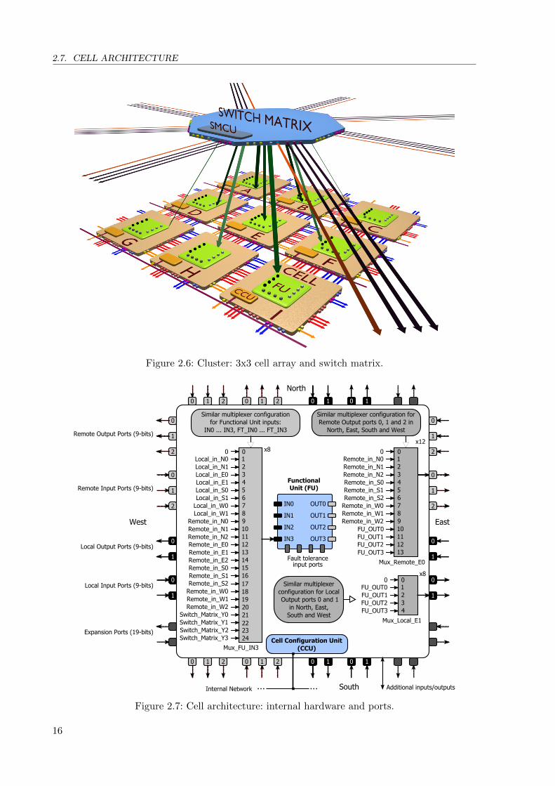
2.7. CELL ARCHITECTURE
Figure 2.6: Cluster: 3x3 cell array and switch matrix.
:
Remote_in_N.
:
.:
..
.A
,T
Local_in_N.Local_in_E:Local_in_E.
Remote_in_N,Remote_in_E:Remote_in_E.Remote_in_E,Remote_in_S:Remote_in_S.
.,
.T
.d
.k
Local_in_S:Local_in_S.
Local_in_W:Local_in_W.
Remote_in_N:
dkA/89
.Local_in_N:
Remote_in_W:Remote_in_W.Remote_in_W,
Remote_in_S,
Switch_Matrix_Y.Switch_Matrix_Y,Switch_Matrix_YT
Switch_Matrix_Y:
./
.8
.9,:,.,,,T,d
RemoteYOutputYPortsY-9Ibitsb
ExpansionYPortsY-.9Ibitsb
Mux_Remote_E:
Mux_FU_INT
Yx8
SimilarYmultiplexerYconfigurationYforYFunctionalYUnitYinputs:Y
IN:YfffYINTUYFT_IN:YfffYFT_INT
SimilarYmultiplexerYconfigurationYforYRemoteYOutputYportsY:UY.YandY,YinY
NorthUYEastUYSouthYandYWest
North
East
South
West
Cell Configuration Unit (CCU)
:
.
,
:
.
:
.
:
.
,
: :
,T
FU_OUT.FU_OUT,FU_OUTT d
.FU_OUT:
:
FU_OUT:
:
.:
..
,T
Remote_in_N.Remote_in_N,Remote_in_S:
FU_OUT.FU_OUT,FU_OUTT
.,
.T
Remote_in_S.Remote_in_S,
Remote_in_W:Remote_in_W.Remote_in_W,
dkA/89
.Remote_in_N:
SimilarYmultiplexerYconfigurationYforYLocalYOutputYportsY:YandY.
inYNorthUYEastUYSouthYandYWest
Functional Unit (FU)
:
.
,
:
.
:
.
:
.
,
: . , : . : .: . ,
: . , : . : .: . ,
Mux_Local_E.
RemoteYInputYPortsY-9Ibitsb
LocalYOutputYPortsY-9Ibitsb
LocalYInputYPortsY-9Ibitsb
Yx.,
Yx8
IN: OUT:
FaultYtoleranceYinputYports
IN.
IN,
INT
OUT.
OUTT
OUT,
InternalYNetwork AdditionalYinputsgoutputs
Figure 2.7: Cell architecture: internal hardware and ports.
16

CHAPTER 2. SYSTEM ARCHITECTURE
one being a 9-bit wide bus, 8-bit for data and 1 bit for Read Enable (RE) flag. Additionally, thecell has four expansion input ports, four expansion output ports, a connection with the INETand additional input/output ports.
The cell includes additional ports interconnected with the SM: four 9-bits input ports, four9-bit output ports (FU output ports), one expansion input port and one expansion output port.
The cell includes 28 multiplexers divided in three groups:
I 8 multiplexers connected to the local output ports. These multiplexers allow connecting theFU output ports with the local output port of the cell. These multiplexers are used exclusivelyto connect neighboring cells.
I 12 multiplexers connected to the remote output ports. These multiplexers allow connectingthe remote output port with: (1) the FU output ports and (2) the remote input ports ofthe other sides of the cell, e.g., if the remote output port is in east, the multiplexer allowsconnecting the remote input ports from north, south and west. The remote port is used forconnecting neighboring or remote cells.
I 8 multiplexers connected to the FU input ports. These multiplexers are used to connect localand remote cell input ports when the connection between two cells is in the same component(inputs 1 to 20). They additionally allow connecting FU ports of two different componentsusing the inputs coming from the SM (inputs 21 to 24).
2.7.1 Functional Unit (FU)
The FU is in charge of executing the processes scheduled to the cell. The FU can be describedas a four-core configurable multicomputer [8]. The FU has four 9-bit input ports and four 9-bitoutput ports. There are four additional input ports (ft input ports) used exclusively for the staticFault Tolerance System (FTS) [33].
The internal architecture of the FU is detailed in chapter 3 and annexes A and B. The FTSis described in section 3.7.
2.7.2 Cell Configuration Unit (CCU)
Using a distributed working principle, the CCUs of the cells in the array are responsible forthe execution of the required algorithms for the implementation of the system self-adaptivecapabilities, specifically the self-placement and self-routing algorithms. These algorithms areexecuted by the CCU using the INET and the expansion ports, and they are explained in detailin chapter 4.
2.8 Switch Matrix
The Switch Matrix (SM) allows connecting cells from two different components. Figure 2.8 showsthe port distribution and the internal hardware that is included in the SM.
The SM is connected to its eight adjacent neighbors, each through three input ports andthree output ports (9 bits each). It additionally includes one input and one output expansionport (8 bits each).
The SM is connected to the nine cells (cell A. . . cell I) belonging to the cluster, each one bymeans of four input ports and four output ports (9 bits each). The input ports correspond to theFU output ports of cells, and the output ports correspond to the output of internal multiplexers.In addition, the SM includes nine input and nine output expansion port (8 bits each) connectedto each cell in the cluster.
17

2.9. PIN INTERCONNECTION MATRIX
The Switch Matrix Configuration Unit (SMCU) participates in the component self-routingprocess (section 4.8). In this process, the FU output port of a cell in a given component isconnected to the FU input port of a cell in a different component. The process configures themultiplexers included in the SM.
The SM includes 60 multiplexers divided in two groups:
I 24 multiplexers connected to the SM output ports. These multiplexers are used as start pointof a connection between two components or when a connection has to cross the SM. Thesemultiplexers allow connecting the output port with: (1) the FU output port of any cell inthe cluster (inputs 1 to 36), and (2) the input ports of other sides of the SM (inputs 37 to57), e.g., if the output port is in east, the multiplexer allows connecting the input ports formnorth, northeast, southeast, south, southwest, west and northwest.
I 36 multiplexers connected to the FU input ports of cells. These multiplexers are used to directthe end point of a connection between two components to one of the nine cells belonging tothe cluster. These multiplexers allow connecting the FU input port with: (1) the FU outputport of other cells in the cluster (inputs 25 to 56), e.g., if the output port is in cell A, themultiplexer allows connecting the output ports form cell B. . . cell I, and (2) the input portsof any side of the SM (inputs 1 to 24).
2.9 Pin Interconnection Matrix
The Pin Interconnection Matrix (PIM) is used exclusively for the port interconnection betweencells of two components in different chips. Figure 2.9 shows the port distribution and the internalhardware that is included in the PIM.
The PIM is connected to its three adjacent clusters, each through three input ports and threeoutput ports (9 bits each). It additionally includes one input and one output expansion port (8bits each). The PIM is connected to the INET.
The Pin Interconnection Matrix Configuration Unit (PIMCU) configures the multiplexers inthe component self-routing process, to allow for the interconnection of the FU port of a cell witha pin of the chip. Previously to this configuration, the GCU undertook a negotiation processwith other chips, with the aim of assigning a pin of the chip to connect these components.
The PIM includes 12 multiplexers divided in two groups:
I 9 multiplexers connected to the PIM output ports. These multiplexers are used to connect ainput pin with an output port. This is the start point of a connection between a input pinand the FU input port of the target cell.
I 3 multiplexers connected to the output pins of the PIM. These multiplexers are used toconnect a input port with an output pin. These multiplexers are the last resource used tointerconnect the FU output port of the source cell with the pin of the chip.
2.10 Expansion Signals
The expansion signals are included in the expansion ports of cells, SMs and PIMs. The expansionsignals are used by self-placement and self-routing processes.
The signals con be divided in three categories as outlined below:
I Cell to Cell: The expansion port between cells includes four 19-bit input ports and four19-bit output ports per cell, distributed in north, east, south and west. Each input and output
18

CHAPTER 2. SYSTEM ARCHITECTURE
Input Ports (9-bits)
Output Ports (9-bits)
Expansion Ports (8-bits)
Mux Y0 for Cell_A
0IN_Matrix_North
01,2,34,5,6
22,23,2425,26,27,28
x36
29,30,31,32OUTS_CELL_BOUTS_CELL_COUTS_CELL_D
IN_Matrix_NorthEastIN_Matrix_EastIN_Matrix_SouthEastIN_Matrix_SouthIN_Matrix_SouthWestIN_Matrix_WestIN_Matrix_NorthWest
7,8,910,11,1213,14,1516,17,1819,20,21
OUTS_CELL_EOUTS_CELL_FOUTS_CELL_GOUTS_CELL_HOUTS_CELL_I
33,34,35,3637,38,39,4041,42,43,4445,46,47,4849,50,51,5253,54,55,56
Mux Switch Matrix West OUT0
0
IN_Matrix_North
0
37,38,3940,41,42
55,56,57
5,6,7,8
x24
9,10,11,12OUTS_CELL_BOUTS_CELL_COUTS_CELL_D
IN_Matrix_NorthEastIN_Matrix_EastIN_Matrix_SouthEastIN_Matrix_SouthIN_Matrix_SouthWestIN_Matrix_NorthWest
43,44,4546,47,4849,50,5152,53,54
OUTS_CELL_EOUTS_CELL_FOUTS_CELL_GOUTS_CELL_HOUTS_CELL_I
13,14,15,1617,18,19,2021,22,23,2425,26,27,2829,30,31,3233,34,35,36
1,2,3,4 OUTS_CELL_A
Similar multiplexer configuration for OUT0,OUT1 and OUT2 for Switch Matrices at
North, NorthEast, East, SouthEast, South, SouthWest, West and NorthWest.
Similar multiplexer configuration for signals Y0, Y1, Y2 and Y3, connected to FU inputs multiplexer
of Cells: A, B, C, D, E, F, G, H and I
0
1
2
0
1
2
01
2
01
2
012012
01
2
01
201
2
01
2
01
2
01
2
0 1 2 0 1 2
0
1
2
0
1
2
North
NorthEast
East
SouthEast
South
SouthWest
West
NorthWest
Switch Matrix Configuration Unit (SMCU)
Figure 2.8: Architecture of Switch Matrix.
Input Ports (9-bits)
Output Ports (9-bits)
Expansion Ports (8-bits)
Mux PIN0
0IN0_Cluster0
selector
012
89
x3
IN2_Cluster2
IN1_Cluster0IN2_Cluster0IN0_Cluster1IN1_Cluster1IN2_Cluster1IN0_Cluster2IN1_Cluster2
34567
Mux Pin Interconnection Matrix Cluster1 OUT2
selector
00
2
x9
3PIN1_INPIN2_IN
1 PIN0_IN
Similar multiplexer configuration for OUT0,OUT1 and OUT2 for connections between Switch and Pin interconnection Matrices in
Cluster_0, Cluster_1 and Cluster_2
Similar multiplexer configuration for
PIN0, PIN1 and PIN2
0
1
2
0
1
2
01
2
01
2
01
2
01
2
0
1
2
0
1
2
Cluster 2
Cluster 1
Cluster 0
Input Pins (9-bits)
Output Pins (9-bits)
Pin Interconnection Matrix Configuration Unit
(PIMCU)
Internal Network Additional inputs/outputs
Figure 2.9: Architecture of Pin Interconnection Matrix.
19

2.11. INTERNAL AND EXTERNAL NETWORKS
port includes 11 signals. Figure 2.10 shows the expansion signals between two cells connectedin east and west ports.
I Cell to Switch Matrix: Each SM includes nine 8-bit input ports and nine 8-bit outputports, for the connection of expansion signals between SM and the cells that belong to thecluster (cell A. . . cell I). Therefore, each cell includes additionally one 8-bit expansion inputport and one 8-bit expansion output port. Figure 2.11 shows the expansion signals betweencell A and SM inside the cluster.
I Switch Matrix to Switch Matrix (or Pin Interconnection Matrix): Each SM includeseight 8-bit expansion input ports and eight 8-bit expansion output ports, for the connectionof expansion signals between SMs across clusters. Figure 2.12 shows the expansion signalsbetween two SMs. The expansion ports between SM and PIMs are the same.
2.10.1 Global Signals for Self-routing Process
Figure 2.13 shows the additional global signals: Routing complete and Enable routing. Thesesignals are the result of a logic OR function between all members of the system that could start orstop a routing process, i.e., CCUs and PIMCUs. When one of these CUs wants to start a routingprocess, it sets its enable routing out signal, enabling the routing capabilities for all members inthe system. Similarly, when any CU wants to terminate the process, it sets the routing completeout signal. The self-routing process is detailed in section 4.6.
2.11 Internal and External Networks
The Internal Network (INET) and External Network (ENET) have been designed to provide thesystem with the necessary functionality to carry out the self-adaptive capabilities, specifically theself-placement and self-routing processes. Since several CUs of the system (CCUs, PIMCUs andGCU) should be able to send and simultaneously receive messages, the interface communicationsystem is based on an adaptation of the I2C Bus Specification [36].
2.11.1 Communication Interface
The INET and ENET are based on two basic signals: serial clock line (SCL) and serial data line(SDA). These signals are the result of a logic AND (organized in rows and columns) betweenthe output signals of all CUs of the system with networking capabilities. When the transmission(tx) process of a CU is in standby, the signals are at high logic level, thus, if all CU are instandby, the result on the SDA and SCL lines will be high. The Figure 2.14 shows the hardwareimplementation for the CUs involved in the INET.
When a CU needs to send a message, the transmission process starts, so that it has toset or clear the appropriate output signals. This way, the message will be visible in SDA andSCL and can be read simultaneously by all CUs of the system, including the transmitter. Thischaracteristic is important in the execution of the self-adaptive algorithms implemented in thesystem. This implies that source cell(s) can get information of other cells without the need totransmit an answer from the target cell(s).
The transmission process could be started by one or more CUs in the chip (simultaneously),this depends on the algorithm that is being executed.
The ENET has a similar configuration to that of the INET. The ENET interconnects theGCUs with the EC.
20

CHAPTER 2. SYSTEM ARCHITECTURE
busy_cell_flag_in_Ecalculate_distance_enable_in_E
distance_in_Eborder_in_E
propagate_in_Elock_in_E
neighbor_in_Eremote_port_in_E
local_port_in_Eid_target_port_in_E
del_connection_in_E
*busy_cell_flag*calculate_distance_enable
*distance*border
propagate_out_Elock_out_E
neighbor_out_Eremote_port_out_E
local_port_out_E*id_target_port_out
del_connection_out_E
6
3
2
6
3
2
busy_cell_flag*calculate_distance_enable*distance*border*propagate_out_Wlock_out_Wneighbor_out_Wremote_port_out_Wlocal_port_out_Wid_target_port_out*del_connection_out_W
busy_cell_flag_in_Wcalculate_distance_enable_in_Wdistance_in_Wborder_in_Wpropagate_in_Wlock_in_Wneighbor_in_Wremote_port_in_Wlocal_port_in_Wid_target_port_in_Wdel_connection_in_W
N19-bitNorth
South
North
South
West East
CELLNA CELLNB
Figure 2.10: Expansion signals between cells1.
propagate_in_matrixlock_in_matrix
id_target_port_in_matrixmux_id_matrix
del_connection_in_matrix
propagate_out_matrixlock_out_matrix
*id_target_port_out*id_source_port_out
del_connection_out_matrix
32
32
propagate_out_cell_Alock_out_cell_Aid_target_port_out*mux_id_cell_Adel_connection_out_cell_A
propagate_in_cell_Alock_in_cell_Aid_target_port_in_cell_Aid_source_port_in_Adel_connection_in_cell_A
8CellIB
CellIC
CellID
CellIE
CellIF
CellIG
CellIH
CellII
CellIASwitchIMatrix
Figure 2.11: Expansion signals between cell and Switch Matrix1.
propagate_in_Elock_in_E
id_target_port_in_Ematrix_port_in_E
del_connection_in_E
propagate_out_Elock_out_E
*id_target_port_outmatrix_port_out_E
del_connection_out_E
32
32
propagate_out_Wlock_out_Wid_target_port_out*matrix_port_out_Wdel_connection_out_W
propagate_in_Wlock_in_Wid_target_port_in_Wmatrix_port_in_Wdel_connection_in_W
8-bit
SwitchBMatrixBA SwitchBMatrixBB
Figure 2.12: Expansion signals between Switch Matrices (including Pin Interconnection Matrix)1.
1Signals marked with * are common for all expansion ports.
21

2.11. INTERNAL AND EXTERNAL NETWORKS
CELLHARRAY Routing_complete
enable_routing_inrouting_complete_in
routing_complete
_out
enable_routing
_out
PIM
00
0
0
enable_routing_inrouting_complete_in
enable_routing_out
routing_complete_out
enable_routing_inrouting_complete_in
enable_routing_out
routing_complete_out
enable_routing_inrouting_complete_in
enable_routing_out
routing_complete_out
0
0
enable_routing_inrouting_complete_in
enable_routing_out
routing_complete_out
enable_routing_inrouting_complete_in
enable_routing_out
routing_complete_out
enable_routing_inrouting_complete_in
enable_routing_out
routing_complete_out
0
0
enable_routing_inrouting_complete_in
enable_routing_out
routing_complete_out
enable_routing_inrouting_complete_in
enable_routing_out
routing_complete_out
enable_routing_inrouting_complete_in
enable_routing_out
routing_complete_out
Enable_routing
PINHINTERCONNECTION
MATRICES
routing_complete_in
SM
routing_complete_in
SMenable_routing_inrouting_complete_in
routing_complete
_out
enable_routing
_out
PIM
SWITCHMATRICES
Figure 2.13: Routing signals implementation.
scl_insda_in
scl_out
sda_out
scl_insda_in
scl_out
sda_out
scl_insda_in
scl_out
sda_out
1
1
scl_insda_in
scl_out
sda_out
scl_insda_in
scl_out
sda_out
scl_insda_in
scl_out
sda_out
1
1
scl_insda_in
scl_out
sda_out
scl_insda_in
scl_out
sda_out
scl_insda_in
scl_out
sda_out
1
1
scl_insda_in
scl_outsda_out
GCU
scl_insda_in
sclout
sdaout
PIM
scl_insda_in
sclout
sdaout
PIM
CELL ARRAYSDA SCL
Figure 2.14: Internal Network implementation.
22

CHAPTER 2. SYSTEM ARCHITECTURE
Figure 2.15: Considerations for Internal and External Networks.
2.11.2 Data Transmission
A transmission consists of three parts: generation of the start condition (or repeated start condi-tion), data bits transmission and generation of the stop condition (or repeated start condition).Figure 2.15 shows necessary considerations for data transmission for INET and ENET, as follows:
I All transactions begin with a start condition and are terminated by a stop condition.I Start condition: a high to low transition on the SDA line while SCL is high.I Stop condition: a low to high transition on the SDA line while SCL is high.I Data validity: The data on the SDA line must be stable during the high period of the clock.
The high or low state of the data line can only change when the clock signal on the SCL lineis low. One clock pulse (SCL) is generated for each data bit transferred.
I The bus stays busy if a repeated start condition is generated instead of a stop condition. Inthis respect, the start and repeated start conditions are functionally identical.
2.11.3 Comparison Process
The algorithms of self-placement and self-routing require the implementation of a data comparisonprocess from one or more cells, to identify the cell with better characteristics for a particularfunction with respect to another cell within the array. The physical implementation of the INETdescribed previously permits this functionality, thus many cells can simultaneously compare thedata while the transmission/reception is being executed. This is possible due to the logic ANDbetween all sda out signals, so that the lowest value will be imposed in a comparison.
An example of a comparison process is shown in Figure 2.16a. Let us assume that four cellssend the following values: sda out1=0x05, sda out2=0x07, sda out3=0x13 and sda out4=0x4B.These values will be compared bit to bit, starting with the most significant bit. The dominantvalue has to be the smallest one. As result of the logic AND, when one of the cells sends a highvalue but on the SDA line it appears a low value, this means that another cell has a better (lower)comparison value. This cell is self-discarded from the comparison and sets its sda out to highvalue for the remaining bits. The cell that terminates the process without being discarded willbe the winner (sda out1 in Figure 2.16a).
If there are two or more cells with the same value for comparison, the winner will be theleftmost uppermost cell in the array. This selection process takes place outside the INET withsome additional bits, by means of the circuit shown in Figure 2.16b. The cells involved in theprocess put a low level in the flip flop, and after a clock pulse, only one of them must continuein low level. This one will be the ”winner cell” of the comparison process.
23

2.12. COMMUNICATION PROTOCOL FOR INTERNAL NETWORK
1 2 3 4 5 6 7 8SCL
sda_out1 = 0x05
sda_out2 = 0x07
sda_out3 = 0x13
SDA
sda_out4 = 0x4B
Forced value imposed by comparison process.
Original value transmited.
(a) Example of the comparison process.1
D Q
1 1 1
D Q D Q
D Q D Q D Q
D Q D Q D Q
(b) Implementation of the cell selection process.
Figure 2.16: Comparison process.
Startcondition Header (40 bits) Arguments depends of
the control field valueStop
condition
Start address32 bits
control2 bits
command6 bits
data0-2056 bits Stop
Start Headercontrol = 01 Stop
Start Headercontrol = 10 Stopack
1 bit
Start Headercontrol = 11 Stop0byte
Start Headercontrol = 00
nBytes8 bits Stop0byte byte1 bytenBytes
Transmission of 1 to 256
data bytes Transmission without
data bytes
Transmission of acknowledge bit
Transmission of comparison byte
(a) Communication protocol for Internal Network.
Startcondition Header (8 bits) Arguments depends of
the control field valueStop
condition
Start control1 bit
command7 bits
data0-2056 bits Stop
Start Headercontro = 0
nBytes8 bits Stop0byte byte1 bytenBytes
Transmission of 1 to 256 data bytes
Start Headercontrol = 1 Stop Transmission without
data bytes
(b) Communication protocol for External Network.
Figure 2.17: Comumnication protocols.
2.12 Communication Protocol for Internal Network
The communication protocol is formed by the grouping of bits that are transmitted and received.This exchange of information for INET takes place between several CUs inside a chip, specificallythe GCU, the PIMCUs and the CCUs. Figure 2.17a shows a detailed description of this protocol.
All bits belonging to the protocol are delimited by the start and stop conditions previouslyexposed. The frame can be divided in two sections: the header and the arguments (or databytes). The 40-bit header is always present in a frame. The arguments sent or received later aredependent on the control bits and the command value. The header fields are described below:
1. address: This 32-bit field is used to identify the cell to which the message is directed. Thisfield includes the id cell and id component, each 16-bit long. The value 0xFFFFFFFF isreserved for broadcasting.
2. control bits: The 2-bit control field specifies the number of data bits after the command.Thus, there may be commands that require or not any additional information, as follows:
I control=00 ⇔ Data bytes: When the command field requires additional information,the 8-bit nBytes field is used. It indicates the number N of bytes that will be sent. Thesebytes may include connection tables, command arguments or information for cells that willbe for program memory and configuration registers.1 ≤ N ≤ 256, nBytes = N − 1
24

CHAPTER 2. SYSTEM ARCHITECTURE
I control=01 ⇔ No data: No additional data bytes are required.I control=10 ⇔ Acknowledge bit: The 1-bit ack field is used as an acknowledgment
mechanism, indicating that the address field sent by a source cell matches with the addressof a target cell.
I control=11 ⇔ Comparison byte: The byte0 is the comparison value that is sent simul-taneously by one or more cells. It is used when required to search the best cell locationwith respect to another to perform a given function (see section 2.11.3 for details).
3. command : The 6-bit command field specifies the action that will take place inside theelement(s) to which the frame is addressed. The commands correspond to the execution ofnecessary algorithms for implementing the self-routing and self-placement processes. The datasent or received later are dependent on the control bits and the command value. The list ofcommands is showed in Table 2.1. The use of this commands and its functionality is explainedin chapter 4.
Command (INET) TX→RX Description
insert first cell GCU→CCUs Commands used for theplacement of the first cell of anew component.
scan first cell CCUs→CCUsend first cell CCU→GCU
insert other cell GCU→CCUs Commands used for theplacement of other cells in acomponent (from the second).Additionally performs the routingof the connections between cellsof the same component alreadyplaced in the array.
scan new cell connections CCUs→CCUsrequest scan affinity value CCU→CCUsscan affinity value CCUs→CCUsset target cell sr CCU→CCUsconnect others to new cell sr CCU→CCUsend other cell CCU→GCU
error routing CCU, PIMCU→GCU Error when there is no routing re-sources available for a connection.
start components connection GCU→CCUsCommands used for theconnection of components.
set target cell sr component CCU→CCUend components connection CCU→GCU, CCUs
configure chip connection CCU→GCU
Additional commands used forthe connection of components indifferent chips. These commandsmust be executed after theplacement and routing of allcomponents.
set target cell sr chip GCU→CCUsearch pin free mb GCU→PIMCUspin free mb PIMCU→GCUset target port mb GCU→PIMCUsstart cell pin connection GCU→CCUscell pin connection conf CCU→GCUstart pin cell connection GCU→PIMCUspin cell connection conf PIMCU→GCUconfigure chip connection conf GCU→CCUs
write configuration registers GCU→CCU Write the ConfigurationRegisters and Program Memoryof Functional Unit processors.
write program memory[0,1,2,3] GCU→CCUwrite FU memory conf CCU→GCU
restart processors GCU→CCUsCommands used for controllingthe Functional Unit processors.
disable processors GCU→CCUsrestart and disable processors GCU→CCUsenable processors GCU→CCUs
Continued on next page
25

2.13. COMMUNICATION PROTOCOL FOR EXTERNAL NETWORK
Command (INET) TX→RX Description
wait GCU→CCUs Commands used for controllingthe Functional Unit processorsincluding ”wait” or ”standby”state.
restart processors wait GCU→CCUsenable processors wait GCU→CCUs
start subprocess[0,1,2,3] CCU→GCU Commands used for execution ofsubprocesses, i.e., run-timeself-configuration.
end subprocess[0,1,2,3] GCU→CCUs
delete component connectionschip
CCU, GCU→CCUsCommands used to delete acomponent in the cell array.delete component connections
confCCU→GCU
delete component chip GCU→CCUsdelete component conf CCUs→GCU
deroute connection other chip PIMCU→GCU Commands used to derouteconnections of component inother chips, which are used fordeleting components.
deroute pin cell connection GCU→PIMCUderoute pin cell connection conf PIMCU→GCUderoute connection other chipconf
GCU→PIMCU
replicate cells CCU→GCUCommands used forself-elimination andself-replication processes.
delete cell connections chip GCU, CCU→CCUsdelete cell connections conf CCU→GCUeliminate cell GCU→CCUeliminate cell conf CCU→GCU
Note: conf = confirmation
Table 2.1: Commands list for Internal Network.
2.13 Communication Protocol for External Network
The comunication protocol for ENET permits to communicate the GCUs in different chips andthe EC. Figure 2.17b shows a detailed description of this protocol.
All bits belonging to the protocol are delimited by the start and stop conditions previouslyexposed. The frame can be divided in two sections: the header and the arguments (or data bytes).The 8-bit header is always present in a frame. The arguments sent or received later are dependenton the control bit and the command value. The header fields are described below:
1. control bit : The 1-bit control field specifies the number of data bits after the command. Thus,there may be commands that require or not any additional information, as follows:
I control=0 ⇔ Data bytes: When the command field requires additional information, the8-bit nBytes field is used. It indicates the number N of bytes that will be sent. These bytesmay include connection tables, command arguments or information for chips that will befor program memory and configuration registers.1 ≤ N ≤ 256, nBytes = N − 1
I control=1 ⇔ No data: No additional data bytes are required.
2. command : The 7-bit command field specifies the action that will take place inside the chip(s).The commands correspond to the execution of necessary algorithms for implementing the
26

CHAPTER 2. SYSTEM ARCHITECTURE
Figure 2.18: 3D representation of the prototype architecture.
self-routing and self-placement processes. The list of commands is showed in Table 2.3. Theuse of these commands and their functionality is explained in chapter 4.
2.14 Prototype architecture
For demonstration purposes, the original architecture previously described has been modified forthe construction of a prototype, due mainly to the physical limitations in the FPGAs used for thesystem implementation. The prototype shown in Figure 2.18 has the following characteristics:
I The prototype has been developed in two chips, each one is a Virtex4 Xilinx FPGA (XC4VLX60),with an utilization rate close to 80% of their capacity.
I Each chip consists of a cluster that was reduced to a 2x2 cell array (this includes the SM),one PIM, one Control Microprocessor (CµP) and the GCU.
I The Internal and External networks were implemented.
I The system supports up to 32 processors working in parallel.
I The system implements all self-adaptive capabilities described in this document.
I All system components are described in VHDL. The CµP was implemented using the EDKdesign tool from Xilinx, which implements the MicroBlaze microprocessor; it is programmed inC language by means of the Xilinx Platform Studio (XPS) and Xilinx Software DevelopmentKit.
I The programming and compilation of a entire project in system is manually performed usingthe SANE Project Developer (SPD) (See chapter 5 and appendix D).
Figure 2.19 shows the block diagram of a chip in the prototype. This design permits to havethe same code description for both chips, the only difference is in the allocation of pins for eachchip (files *.ucf).
The External Controller (EC) was replaced by the Control Microprocessor (CµP) inside chips.It should be noted that CµP is implemented in both chips but only one of them must assume thecontrol for the system configuration (master chip). The CµP of the master chip is responsible
27

2.14. PROTOTYPE ARCHITECTURE
Command (ENET) TX→RX Description
synchronize chips EC→GCUs Initial synchronization between chips
start contest winner chip EC→GCUs Contest for the execution of a processin a chip.
cell number new component EC→GCUs
Insertion of a component in a chip.insert first cell EC→GCUend first cell GCU→ECinsert other cell EC→GCUend other cell GCU→EC
error routing GCU→EC There are no routing resources avail-able for the connection of two cellsin a component.
autoset for components connection EC→GCU
Commands used for connection ofcomponents.
start components connection EC→GCUsearch cell other chip GCU→GCUsrouting cell target chip GCU→GCUsend routing cell target chip GCU→GCUsend components connection GCU→ECerror components connection GCU→EC
set address program memory EC→GCUsWrite the Configuration Registersand Program Memory of FunctionalUnit processors.
write configuration registers EC→GCUswrite program memory[0,1,2,3] EC→GCUswrite FU memory conf GCU→EC
restart processors EC→GCUsCommands used for controlling theFunctional Unit processors.
disable processors EC→GCUsrestart and disable processors EC→GCUsenable processors EC→GCUs
wait EC→GCUs Commands used for controlling theFunctional Unit processorsincluding ”wait” or ”standby” state.
restart processors wait EC→GCUsenable processors wait EC→GCUs
start subprocess[0,1,2,3] GCU→EC Commands used for execution ofsubprocesses, i.e., run-timeself-configuration.
end subprocess[0,1,2,3] EC→GCU
autoset for delete connections EC→GCUs
Commands used to delete acomponent in the cell array.
delete component connections chip EC→GCUderoute connection other chip GCU→GCUsderoute connection other chip conf GCU→GCUsdelete component connections conf GCU→ECdelete component chip EC→GCUsdelete component conf GCU→EC
replicate cells GCU→EC
Commands used forself-elimination andself-replication processes.
delete cell connections chip EC→GCUsdelete cell connections conf GCU→ECeliminate cell EC→GCUseliminate cell conf GCU→ECcell reinsert EC→GCUs
Note: conf = confirmation
Table 2.3: Commands list for External Network.
28

CHAPTER 2. SYSTEM ARCHITECTURE
SCL2_temp 011
CHIP0
SDA2_temp1
SCL2_iniSCL2_out
iSCL2_temp
iSDA2_temp
iSCL2_in
CHIP1
SDA2_iniSDA2_out
iSDA2_in
winning_chip_n_in1
iwinning_chip_n_in
winning_total_n_iniwinning_chip_n_out
iwinning_
total_n_in
MCLR_temp0
iMCLR_temp
MCLR_in
MCLR_totaliMCLR_out iMCLR_total
iMCLR_out
01
01
01
01
01
01
01
GCU
iSCL2_out
iSDA2_out
iwinning_chip_n_out
SCL2_out
SDA2_outwinning_chip_n_out
MCLR_out
cell_00_out0cell_00_out1
cell_11_out3
01
other_signals_for_test
15 LEDs16
63
8
RXTX RSk232
Sim7Test
6
CLUSTER 9
PIN0_outPIN1_outPIN2_out
PIN0_inPIN1_inPIN2_in
DIPkswitch
SW3
SW4
clk_50MHz
PUC
DCMclk_25MHz
12345678
Figure 2.19: Block diagram of a chip in prototype.
(a) Prototype picture. (b) Connector layout
Figure 2.20: Prototype implementation
for implementing the main program for the configuration and execution of system functionality,even during runtime. Because of this, the dip-switch in positions 1 and 2 allows the selection ofthe master and slave chip.
The CµP through the GCU in both chips is responsible for controlling the self-placement,self-routing and the execution of any other self-adaptive processes.
Figure 2.20 shows a picture of the physical implementation of the prototype and the layoutof the connection board.
29

2.15. CONCLUSIONS
The output of cells can be visualized in the leds included in the cards. This output is usefulfor the test of applications in the system. The dip-switch in positions 3 to 8 allows to select theoutput of cells and other internal process for debugging purposes.
2.15 Conclusions
This chapter describes the hardware components involved in the self-adaptive architecture pre-sented in this dissertation.
The chapter starts with the definition of the four conceptual layers defined for the architecture.Afterwards, some details for the configuration of an application are detailed, specifically thedescription of a connection between cells, which is critical in the definition of the architecture.
The system is presented in a top-down approach, starting for a general overview of the entiresystem, which includes several chips interconnected with an External Controller (EC). Afterwards,the two layer architecture of the chip is detailed. This is the physical implementation of thesystem, and includes a cluster array interconnected with a Global Configuration Unit (GCU)and Pin Interconnection Matrices (PIMs). The cluster is composed of a 3x3 cell array and aSwitch Matrix (SM). The input and output ports and the internal hardware of each componentis detailed in the corresponding section.
This chapter also describes in detail the communication protocols for Internal Network (INET)and External Network (ENET). These networks participate actively in the self-adaptive processesas discussed in the following chapters. The general description of the prototype implemented fortesting the architecture is presented at the end of the chapter.
30

Chapter 3
Functional Unit Architecture
Life would be tragic if it weren’t funny.
La vida serıa tragica sino fuera graciosa.
Stephen Hawking (1942)
Abstract: This section shows the functional description of the cell Functional Unit. It
includes description of cores, configuration modes, and details of principal parts of processors
like Data and Program Memories. Appendices A and B provide complementary information
over the functionality of processors, showing details about the Instruction Set and Data
Memory Registers respectively.
3.1 General Description
The Functional Unit (FU) is in charge of executing the processes scheduled to the cell or, fromother point of view, the FU provides the processing capabilities to the cell. The FU can bedescribed as a four-core configurable multicomputer [8]. The FU has twelve configuration modesthat allows implementing between one to four processors, which can be configured for dataprocessing of 8, 16, 24 or 32 bits.
The architecture of the FU could be composed of logic gates, LUTs, ALUs or any configurabledigital system, but due to the hardware necessary to carry out the self-adaptive principles, inorder to balance overhead, it has been decided to include a configurable digital element withgreater complexity. The need for a system with general purpose computation capabilities leadto the design of the FU as a set of configurable processors with Harvard architecture.
Figure 3.1 shows a block diagram of the cell, which includes the FU and the Cell ConfigurationUnit (CCU). Additionally, the cell includes multiplexers that allows the interconnections ofFU ports between cells. The CCU and the multiplexers provide support for the self-adaptivecapabilities of cells. The FU has the following main characteristics:
I Four 9-bit input ports.
I Four 9-bit output ports.
I Four cores: each core contains the digital elements necessary for the construction of a processor.
I Output Multiplexing System (OMS): the OMS permits the cores to write data to the outputports.
31

3.2. FU PORTS
Local Ports
Remote Ports
Expansion Ports
Internal Network
FUNCTIONAL UNIT
InputPorts
OutputPorts
CELL CONFIGURATIONUNIT (CCU)
Fault Tolerance Input Ports
FU
FTCSR
PORTS
CORE1 CORE2 CORE3
Outputs_Multiplexing_System
flags_with_CCU
CORE0
OUT0
OUT1
OUT2
OUT3
IN0
IN1
IN2
IN3
FT_IN0 FT_IN1 FT_IN2 FT_IN3
ft_error_flagFault_Tolerance_System
(FTS)
CELL MODE
SUBPCSR
Figure 3.1: Functional Unit architecture.
I Fault Tolerance System (FTS): the FTS enables the system to continue operating properlyin the event of failure of some of its processors. If the FTS detects a hardware failure in aprocessor, the cell or cells involved in the failure could be self-replicated in another locationinside the array. Therefore the cell will be self-discarded for future self-placement processes.
I Four 9-bit fault-tolerance input ports used exclusively for FTS when enabled.
I PORTS Register: configures the OMS allowing write operations over FU output ports.
I FTCSR Register: configures the FTS and the OMS.
I MODE Register: sets the configuration mode of cell, i.e., configures how the cores are groupedto build from one to four processors in FU.
I SUBPCSR Register: interface between FU and CCU for the execution of subprocesses, i.e., itallows the execution of runtime self-configuration capability of the system.
3.2 FU Ports
The FU input ports can be interconnected with the FU output ports of two cells through thelocal and remote cell ports or through the Switch Matrices. This connection is performed by theself-routing process (Chapter 4).
The 9-bit FU input and output ports are composed of an 1-bit Read Enable (RE) signal and8-bit of data (including the Fault Tolerance input ports). When a data is written to the registerrelated to the output port, it is generated a pulse in the ninth bit of the FU port. The RE pulseis one clock-cycle.
Figure 3.2 shows an example of RE pulse when different data bytes are written in an outputregister. The data (ALU) and the enable signal from a core permits to write the output registerassociated to the FU output, and additionally permits to generate the RE pulse. When two ormore output port register are written simultaneously, i.e., for 16, 24 or 32-bit processors, the REbit in each port of FU has the same behavior.
The RE pulse of an input port is used to detect when a data has been written in the port.For this purpose, the special instruction BLMOV is used.
32

CHAPTER 3. FUNCTIONAL UNIT ARCHITECTURE
From1COREX
FU1Output1PortOUTY1_9-bitG
clk
8-bit1data D0 D1 D2 D3 D4
1-bit1enable1-1enX
8-bit1Register1-1OUTY_REG D011111111111111 D1 D2 D3 D4
1-bit1pulse1-1RE
Figure 3.2: Read Enable pulse example.
3.3 Architecture of Processors
Throughout this document, the terms ”cores” and ”processors” are used frequently. The followingsections clarify its difference from the point of view of the architecture presented.
3.3.1 Cores
The core can be described as a set of digital elements that could be used to build a processor(Figure 3.3). The FU has four cores, and each core includes the next principal components:
I General Purpose Registers (GPRs), 8 bytes, R0 to R7.I 8-bit ALU.I Code Condition Register (CCR).I Program Counter.I Control Memory.I Program Memory (64 instructions capacity).
Most of this components have the same characteristics for all cores, except the ALU andthe Program Counter. Each ALU includes specific hardware that supports the execution ofinstructions depending of the length of the processing data. The length of the Program Counteris different for each core: 8-bit for CORE0, 6-bit for CORE1 and CORE3, and 7-bit for CORE2,this is related to the size of the Program Memory that a core can handle in a specific configurationmode.
3.3.2 Processor
The processor is composed of the elements of one or more cores. Therefore, the FU can havebetween one to four processors. Figure 3.3 shows an example of the construction of threeprocessors: the first is an 8-bit or 16-bit processor based on two cores, the second and thirdare 8-bit processors based in one core each. In this figure, the processor P0 shows the basicarchitecture of any processor in the FU. Note that there are bus lines denoted by ’N’, whichindicated that the data processing capability could be for 8, 16, 24 or 32 bits. The following aresome consideration of processors in FU:
I The cores can be grouped in order to build a processor with more capacity. The programmemories are added always in length, whilst the Data Memory can be added in length and/orwidth.
I The cores are grouped from left to right. The leftmost includes the most significant byte whenthe data processing is for 16, 24 or 32 bits.
I The Program Counter controls the sequence of the program. The processors includes condi-tional and unconditional instructions to modify this sequence.
33
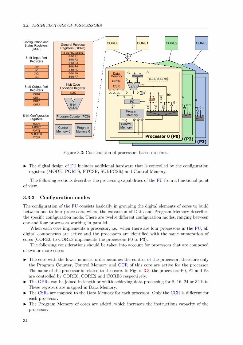
3.3. ARCHITECTURE OF PROCESSORS
8Lbit0Configuration0Registers
8Lbit0Input0PortRegisters
8Lbit0Output0PortRegisters
8-bitALU0
Program5Counter5fPC0d
ControlMemory50
ProgramMemory50
CORE1
N N
N N
8
8666
5-7 8 66
10
bb
DataMemory
GPRs
CSR ALU
Z CPCPC
Cout
z
ProgramMemory
ControlMemory
N 8
Processor 0 (P3)
N0=0[8A016A024A032]
N N
N N
8
8666
5-7 8 66
10
bb
DataMemory
GPRs
CSR ALU
Z CPCPC
Cout
z
ProgramMemory
ControlMemory
N 8
Processor 0 (P2)
N0=0[8A016A024A032]
Configuration5and5Status5Registers5
fCSRd
IN0IN1IN2IN3
OUT0OUT1OUT2OUT3
8Lbit0Code0Condition0Register
CCR0
General5Purpose5Registers5fGPR0d
8Lbit0REGISTER08Lbit0R18Lbit0R28Lbit0R38Lbit0R48Lbit0R58Lbit0R68Lbit0R7
MODEFAMILYPORTS
SUBPCSRFTCSR
CORE0 CORE2 CORE3
N N
N N
8
8
666
5-7 8 66
10
bb
DataMemory
GPRs
CSR ALU
Z CPCPC
Cout
z
ProgramMemory
ControlMemory
N 8
Processor 0 (P0)
N0=0[8A016A024A032]
Figure 3.3: Construction of processors based on cores.
I The digital design of FU includes additional hardware that is controlled by the configurationregisters (MODE, PORTS, FTCSR, SUBPCSR) and Control Memory.
The following sections describes the processing capabilities of the FU from a functional pointof view.
3.3.3 Configuration modes
The configuration of the FU consists basically in grouping the digital elements of cores to buildbetween one to four processors, where the expansion of Data and Program Memory describesthe specific configuration mode. There are twelve different configuration modes, ranging betweenone and four processors working in parallel.
When each core implements a processor, i.e., when there are four processors in the FU, alldigital components are active and the processors are identified with the same numeration ofcores (CORE0 to CORE3 implements the processors P0 to P3).
The following considerations should be taken into account for processors that are composedof two or more cores:
I The core with the lower numeric order assumes the control of the processor, therefore onlythe Program Counter, Control Memory and CCR of this core are active for the processor.The name of the processor is related to this core. In Figure 3.3, the processors P0, P2 and P3are controlled by CORE0, CORE2 and CORE3 respectively.
I The GPRs can be joined in length or width achieving data processing for 8, 16, 24 or 32 bits.These registers are mapped in Data Memory.
I The CSRs are mapped to the Data Memory for each processor. Only the CCR is different foreach processor.
I The Program Memory of cores are added, which increases the instructions capacity of theprocessor.
34
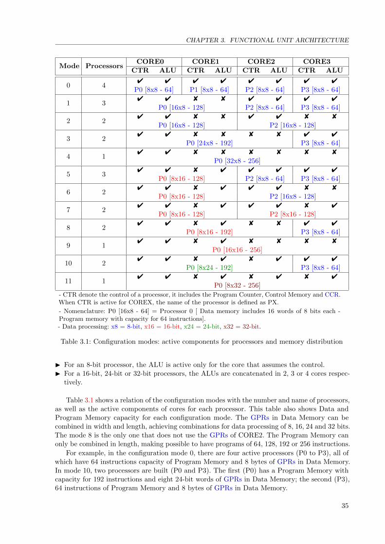
CHAPTER 3. FUNCTIONAL UNIT ARCHITECTURE
Mode ProcessorsCORE0 CORE1 CORE2 CORE3
CTR ALU CTR ALU CTR ALU CTR ALU
0 44 4 4 4 4 4 4 4
P0 [8x8 - 64] P1 [8x8 - 64] P2 [8x8 - 64] P3 [8x8 - 64]
1 34 4 8 8 4 4 4 4
P0 [16x8 - 128] P2 [8x8 - 64] P3 [8x8 - 64]
2 24 4 8 8 4 4 8 8
P0 [16x8 - 128] P2 [16x8 - 128]
3 24 4 8 8 8 8 4 4
P0 [24x8 - 192] P3 [8x8 - 64]
4 14 4 8 8 8 8 8 8
P0 [32x8 - 256]
5 34 4 8 4 4 4 4 4
P0 [8x16 - 128] P2 [8x8 - 64] P3 [8x8 - 64]
6 24 4 8 4 4 4 8 8
P0 [8x16 - 128] P2 [16x8 - 128]
7 24 4 8 4 4 4 8 4
P0 [8x16 - 128] P2 [8x16 - 128]
8 24 4 8 4 8 8 4 4
P0 [8x16 - 192] P3 [8x8 - 64]
9 14 4 8 4 8 8 8 8
P0 [16x16 - 256]
10 24 4 8 4 8 4 4 4
P0 [8x24 - 192] P3 [8x8 - 64]
11 14 4 8 4 8 4 8 4
P0 [8x32 - 256]
- CTR denote the control of a processor, it includes the Program Counter, Control Memory and CCR.When CTR is active for COREX, the name of the processor is defined as PX.
- Nomenclature: P0 [16x8 - 64] = Processor 0 [ Data memory includes 16 words of 8 bits each -Program memory with capacity for 64 instructions].- Data processing: x8 = 8-bit, x16 = 16-bit, x24 = 24-bit, x32 = 32-bit.
Table 3.1: Configuration modes: active components for processors and memory distribution
I For an 8-bit processor, the ALU is active only for the core that assumes the control.I For a 16-bit, 24-bit or 32-bit processors, the ALUs are concatenated in 2, 3 or 4 cores respec-
tively.
Table 3.1 shows a relation of the configuration modes with the number and name of processors,as well as the active components of cores for each processor. This table also shows Data andProgram Memory capacity for each configuration mode. The GPRs in Data Memory can becombined in width and length, achieving combinations for data processing of 8, 16, 24 and 32 bits.The mode 8 is the only one that does not use the GPRs of CORE2. The Program Memory canonly be combined in length, making possible to have programs of 64, 128, 192 or 256 instructions.
For example, in the configuration mode 0, there are four active processors (P0 to P3), all ofwhich have 64 instructions capacity of Program Memory and 8 bytes of GPRs in Data Memory.In mode 10, two processors are built (P0 and P3). The first (P0) has a Program Memory withcapacity for 192 instructions and eight 24-bit words of GPRs in Data Memory; the second (P3),64 instructions of Program Memory and 8 bytes of GPRs in Data Memory.
35

3.4. DATA MEMORY
3.4 Data Memory
The Data Memory is 8, 16, 24 or 32 bit and it is composed of 1, 2, 3 or 4 blocks of General-PurposeRegisters (GPRs) and 14 Configuration and Status Registers (CSRs).
Data memory access is performed through three buses, two for reading and one for writing.This way, a processor could read two registers, perform the desired operation and store the resultin a third register, all in a single clock pulse.
3.4.1 General Purpose Registers (GPRs)
Each core includes eight 8-bit General Purpose Registers (GPRs), which are mapped in DataMemory according to the configuration mode selected. The grouping of these blocks is includedin the Data Memory map shown later in this section.
3.4.2 Configuration and Status Registers (CSRs)
Appendix B includes a detailed description of the CSRs, which can be configured properly forany application designed for the system. All CSRs are 8-bit, below is presented a functionaldescription of these registers.
Output Port Registers (OUT0 . . . OUT3): The 8-bit OUTX register is connected directlyto the 8 less significant bits of FU output port X. The ninth bit of FU corresponds to RE bit asexplained in section 3.2. For a correct write operation of any OUTX register, it is necessary tobe sure that register PORTS is configured properly.
Input Port Registers (IN0 . . . IN3): The 8-bit INX represent the actual data in the 8 lesssignificant bits of FU input port X, or from other point of view, the data in the output portregister of a cell connected to this port. These are read-only registers. The RE pulse in an inputport is used to detect when data has been written in the port. The special instruction BLMOVis used for this purpose.
Code Condition Register (CCR): The CCR is composed of three bits: TA (Thread Active),which indicates if the execution thread has finished or not. The Z and C elements correspondto the flags that indicate when an operation is zero and when the operation has generated acarry respectively. The instruction END is the only one able to stop the execution of the thread(TA ← 0).
Configuration Mode Register (MODE): The 8-bit MODE register is used for the configu-ration mode of the FU. Section 3.3.3 shows the twelve possible configuration modes for FU. Thisis a read only register, therefore a configuration mode can not be modified by a processor.
Famiy Register (FAMILY): The 8-bit FAMILY register was implemented to identify thefamily of the execution thread to which it belongs. The functionality of this register is reservedfor future implementations, where a new programing paradigm [29] [30] [32] could be used toimprove the functionality of the architecture.
Ports Configuration Register (PORTS): The 8-bit PORTS register configures the OutputMultiplexing System in FU. This register configures the path between the ALU of a core andthe OUTX register for a write operation over the FU output port.
Subprocesses Configuration and Status Register (SUBPCSR): The 8-bit SUBPCSRconfigures the execution of subprocesses. Any component in the system can start the executionof one to four subprocesses for dynamic reconfiguration in the system.
36

CHAPTER 3. FUNCTIONAL UNIT ARCHITECTURE
Fault-tolerance Configuration and Status Register (FTCSR): The 8-bit FTCSR config-ures the Fault-tolerance system that permits to detect a hardware failure in desired processorsin the system (See section 3.7 for details).
3.4.3 Data Memory Map
Figure 3.4 shows the memory map for all possible processor in FU. Each memory map has atable that indicates the mode and the processor associated. For 8-bit processors, the GPRs ofcores are joined lengthwise, which allows to increase the user GPRs in Data Memory.
For 16-bit processors in modes 5, 6, 7 and 8, the GPRs are joined widthwise, whereas formode 9 the GPRs are joined lengthwise and widthwise as showed in figure. For 24-bit and 32-bitprocessors the GPRs are joined widthwise.
When there are more than one processor in the FU, it is important to note that all processorscan read any INX register, but only one processor can write a specific OUTX register, thisconfiguration must be performed in the PORTS register. Note that for 16, 24 and 32-bit processors,the ports IN0 and OUT0 represents the most significant byte for data processing.
3.5 Program Memory and Instructions Set
The FU includes four blocks of Program Memory (one on each core). Each block can store upto 64 instructions (64x25 bits). The Program Memory is joined depending on the configurationmode (see Table 3.1) increasing the instructions capacity for a processor.
Each 25-bit word in the Program Memory corresponds to one instruction. This word isdivided in operation code (OPCODE) and the arguments. The OPCODE is 5-bit or 7-bit andthe arguments could use the remaining bits depending on the instructions.
The instruction set is composed of 44 instructions, which includes arithmetic, logic, shift,branch, conditional branch and special instruction for the execution of microthreads [30].
Appendix A includes a detailed description of the instruction set for any processor in theFU.
3.6 Output Multiplexing System
Figure 3.5 shows a block diagram of Output Multiplexing System (OMS). The registers PORTSand FTCSR configure the core that is selected to perform a write operation over a specific OUTregister. Note that any OUT register can be written by only one core.
When the FTS is disabled, the PORTS register allows for configuring the path between thedata bus of a core and the OUT register, and also permits to configure the signal en outX, thatenables the write operation over the register. The enable signals (en outX) are generated by thecore that assumes the control of the processor. These signals are used for loading the outputregister and for the generation of the Read Enable (RE) pulse in the FU output ports.
When the FTS is enabled, the register FTCSR has control priority over PORTS register asshown in Table 3.2. See section 3.7 for details.
3.7 Fault Tolerance System (FTS)
The FTS enables the system to continue operating properly in the event of the failure of some ofits processors. When a failure is detected by the FTS, the FU notifies the problem to the CCU,which starts the appropriate self-adaptive process for the replication of the damaged cells.
37
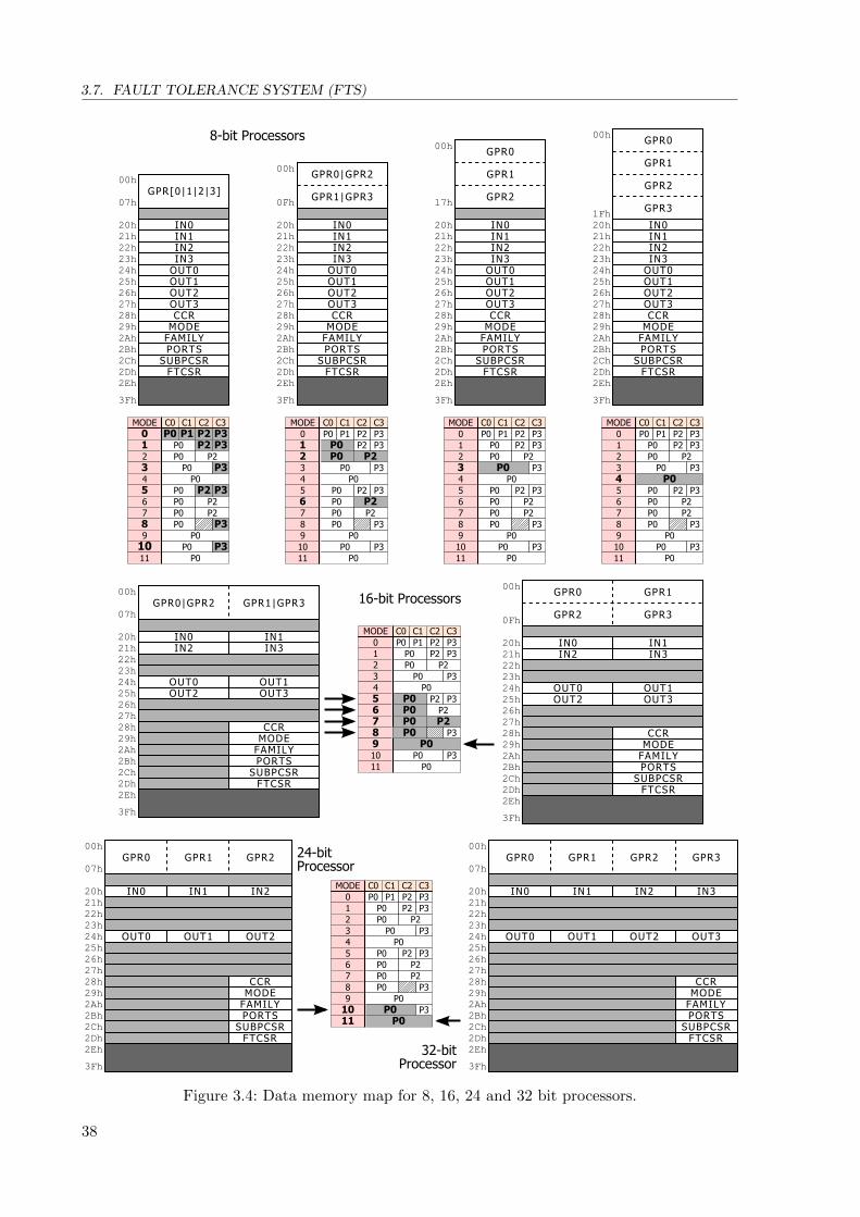
3.7. FAULT TOLERANCE SYSTEM (FTS)
IN020hIN121hIN222hIN323h
OUT024hOUT125hOUT226hOUT327hCCR28h
MODE29hFAMILY2AhPORTS2Bh
SUBPCSR2ChFTCSR2Dh
GPR[0|1|2|3]00h
07h
2Eh
3Fh
IN020hIN121hIN222hIN323h
OUT024hOUT125hOUT226hOUT327hCCR28h
MODE29hFAMILY2AhPORTS2Bh
SUBPCSR2ChFTCSR2Dh
2Eh
3Fh
GPR000h
1Fh
GPR1
GPR2
GPR3
IN020hIN121hIN222hIN323h
OUT024hOUT125hOUT226hOUT327hCCR28h
MODE29hFAMILY2AhPORTS2Bh
SUBPCSR2ChFTCSR2Dh
2Eh
3Fh
GPR0|GPR200h
0Fh GPR1|GPR3
IN020hIN121hIN222hIN323h
OUT024hOUT125hOUT226hOUT327hCCR28h
MODE29hFAMILY2AhPORTS2Bh
SUBPCSR2ChFTCSR2Dh
2Eh
3Fh
GPR000h
17h
GPR1
GPR2
P2C0MODE
01234567891011
C1 C2 C3P0 P1 P3
P3
P3P2
P3
P0P0 P2
P0P0 P2P0 P2
P0
P0P0
P0
P0
P2 P3
P3P0
MODE C0 C1 C2 C3P2P0 P1 P3
P3
P3P2
P3
P0P0 P2
P0P0 P2P0 P2
P0
P0P0
P0
P0
P2 P301234567891011
P3P0
MODE C0 C1 C2 C3P2P0 P1 P3
P3
P3P2
P3
P0P0 P2
P0P0 P2P0 P2
P0
P0P0
P0
P0
P2 P301234567891011
P3P0
MODE C0 C1 C2 C3P2P0 P1 P3
P3
P3P2
P3
P0P0 P2
P0P0 P2P0 P2
P0
P0P0
P0
P0
P2 P301234567891011
P3P0
20h21h22h23h24h25h26h27h28h29h2Ah2Bh2Ch2Dh
GPR0|GPR200h
07h
2Eh
3Fh
IN0 IN1IN2 IN3
OUT0 OUT1OUT2 OUT3
CCRMODE
FAMILYPORTS
SUBPCSRFTCSR
GPR1|GPR3
20h21h22h23h24h25h26h27h28h29h2Ah2Bh2Ch2Dh
GPR2
00h
0Fh
2Eh
3Fh
IN0 IN1IN2 IN3
OUT0 OUT1OUT2 OUT3
CCRMODE
FAMILYPORTS
SUBPCSRFTCSR
GPR3
GPR0 GPR1
MODE C0 C1 C2 C3P2P0 P1 P3
P3
P3P2
P3
P0P0 P2
P0P0 P2P0 P2
P0
P0P0
P0
P0
P2 P301234567891011
P3P0
MODE C0 C1 C2 C3P2P0 P1 P3
P3
P3P2
P3
P0P0 P2
P0P0 P2P0 P2
P0
P0P0
P0
P0
P2 P301234567891011
P3P0
20h21h22h23h24h25h26h27h28h29h2Ah2Bh2Ch2Dh
GPR000h
07h
2Eh
3Fh
OUT2
CCRMODE
FAMILYPORTS
SUBPCSRFTCSR
GPR2GPR1
OUT1OUT0
IN2IN1IN0 20h21h22h23h24h25h26h27h28h29h2Ah2Bh2Ch2Dh
GPR000h
07h
2Eh
3Fh
OUT2
CCRMODE
FAMILYPORTS
SUBPCSRFTCSR
GPR2GPR1
OUT1OUT0
IN2IN1IN0
OUT3
IN3
GPR3
8-bit-Processors
16-bit-Processors
24-bit-Processor
32-bit-Processor
Figure 3.4: Data memory map for 8, 16, 24 and 32 bit processors.
38

CHAPTER 3. FUNCTIONAL UNIT ARCHITECTURE
PORT0
OUT0
OUT0_REG OUT1_REG OUT2_REG OUT3_REG
PORT1 PORT2 PORT3
PORTSERegisterPORT0PORT1PORT2PORT3
01234567
8-bitEdataEfromEALU
1-bitEREEpulseEandE8-bitEdataR
S
Q
en_out0
OUT1
R
S
Q
en_out1
OUT2
R
S
Q
en_out2
OUT3
R
S
Q
en_out3
FTCSR
1 320Mux3
1 320Mux2
1 320Mux1
1 320Mux0
PORT0
CORE0
en_out0_c0en_out1_c0en_out2_c0en_out3_c0
CORE1
en_out0_c1en_out1_c1en_out2_c1en_out3_c1
CORE2
en_out0_c2en_out1_c2en_out2_c2en_out3_c2
CORE3
en_out0_c3en_out1_c3en_out2_c3en_out3_c3
en_out0_c0
1 320Mux00
en_out0_c1en_out0_c2
en_out0_c3
en_out0
PORT0
FTCSR
en_out1_c0
1 320Mux11
en_out1_c1en_out1_c2
en_out1_c3
en_out1
PORT1
FTCSR
en_out2_c0
1 320Mux22
en_out2_c1en_out2_c2
en_out2_c3
en_out2
PORT2
FTCSR
en_out3_c0
1 320Mux33
en_out3_c1en_out3_c2
en_out3_c3
en_out3
PORT3
FTCSR
FALU0 FALU1 FALU2 FALU3
Figure 3.5: Block diagram of Output Multiplexing System.
ft controls en out0 mux0 en out1 mux1 en out2 mux2 en out3 mux3
1 - 1 - 5 1 FALU0 PORT1* PORT2* PORT3*1 - 1 - 6 1 FALU0 1 FALU1 PORT2* PORT3*1 - 1 - 7 1 FALU0 1 FALU1 1 FALU2 PORT3*1 - 1 - 8 1 FALU0 1 FALU1 1 FALU2 1 FALU3
1 - 1 - others PORT0* PORT1* PORT2* PORT3*0 - X - X PORT0* PORT1* PORT2* PORT3*
ft controls ↔ ft enable - ft redundant cell - ft mode
* The value of en outX y muxX depends of PORTX value.
Table 3.2: Output Multiplexing System operating table.
The FTS consists of a specific hardware that allows the comparison of two identical processorseach time that a instruction is executed, that means each clock cycle. This involves the comparisonof 2, 4, 6 or 8 cores, depending of the configuration mode of the FTS (FT mode).
These processors that will be compared are defined as working and redundant. They mustshare the same inputs, but on the other hand, the working processor takes over writing theoutput ports, because two outputs can not be routed to the same location. There may be one ortwo cells participating in the FTS. These cells are called primary and redundant. The primarycell is mandatory and includes working processors. This cell may or may not include redundantprocessors. The redundant cell is optional and includes only redundant processors.
Figure 3.6 shows the block diagram of FTS, which is only active when FTS is enabled and itis the primary cell (signals ft enable and not ft redundant cell). Table 3.3 shows the data buscomparisons available for FTS. Note that FT modes 0 to 4 only perform comparisons with databus from the same cell, whilst FT modes 5 to 8 perform comparison between data buses of thecell with FT input ports, which suppose a connection between the redundant cell and primarycell.
When the redundant cell is used, the OMS allows to write constantly the data bus of coresto the FU output ports as described in Figure3.5 and Table 3.2.
39

3.7. FAULT TOLERANCE SYSTEM (FTS)
1 20Mux0
ft_enable
ft_redundant_cellft_en
CORE0 FALU0
FT_internal_reg0
CORE1 FALU1
FT_internal_reg1
CORE2 FALU2
FT_internal_reg2
CORE3 FALU3
FT_internal_reg3
ft_en
FT_internal_reg1
FT_internal_reg2
FT_IN0(7:0)
10Mux1
FT_internal_reg3
FT_IN1(7:0)
10Mux2
FT_internal_reg3
FT_IN2(7:0)
CMP0
FT_internal_reg0
ft_en CMP1
FT_internal_reg1
ft_en CMP2
FT_internal_reg2
ft_en CMP3
FT_internal_reg3
ft_en
FT_IN3(7:0)30 2 4 5Mux3
1
CMP0 CMP2
CMP2
CMP0 CMP0CMP1
CMP3
CMP0CMP1CMP2
CMP0CMP1CMP2
E
D Q
ft_error_flag
ft_en
Figure 3.6: Fault Tolerance System.
FT mode Comparison Mux0 Mux1 Mux2 Mux3
0 F0⇔F1 0 X X 01 F0⇔F1 & F2⇔F3 0 X 0 12 F2⇔F3 X X 0 23 F0⇔F2 1 X X 04 F0⇔F2 & F1⇔F3 1 0 X 35 F0⇔F0* 2 X X 06 F0⇔F0* & F1⇔F1* 2 1 X 37 F0⇔F0* & F1⇔F1* & F2⇔F2* 2 1 1 48 F0⇔F0* & F1⇔F1* & F2⇔F2* & F3⇔F3* 2 1 1 5
FX denotes a data bus from ALU in COREX (FALUX). ⇔ denotes a comparion between cores. &denotes a logic AND. * denotes a data bus from the redundant cell (a connection between FUs ofprimary and redundant cell is assumed).
Table 3.3: Multiplexers configuration for Fault Tolerance System in primary cell.
3.7.1 Fault Tolerance Input Ports
When the redundant processor is included in the same cell where the working processor is located,the FT input ports are not used, and the FTS only performs comparison between cores of thecell. In this case the redundant cell is not used (FT modes 0 to 4).
Otherwise, when the redundant processor is located in the redundant cell, the FTS of theprimary cell must perform a comparison between cores of different cells, in this case the OMSof the redundant cell must drive the output of the data flow of the core(s) to the output of thecell (RE is set to logic 1), which in turn should be connected to the FT inputs of the FU of theprimary cell that includes the working processor (FT modes 5 to 8).
When the FTS is enabled in the redundant cell, the register FTCSR has priority over PORTSregister to control the OMS as shown in Table 3.2. For example, in FT mode 5 the data bus ofCORE0 is routed directly to the OUT0 REG (mux0=FALU0 and en out0=1 in Figure 3.5). InFT mode 8 all cores are routed directly to the respective OUTX register.
The FU includes four FT input ports. These ports must be interconnected by user with theoutput ports of the redundant cell when the FTS is enabled. The number of ports depends onthe configuration mode of cell and the FT mode.
40

CHAPTER 3. FUNCTIONAL UNIT ARCHITECTURE
FunctionalSUnitSinSPrimarySCell
FunctionalSUnitSinSRedundantSCell
PX WorkingSProcessorSX
RedundantSProcessorSYPY
DB-CX DataSBusSfromSCoreSX
ComparisonSperformedSbySFaultSToleranceSSystemS1FTS6
FT_modeS3S18Nbit6
FT_modeS4S116Nbit6
P0DB-C0,C1,C2,C3
P0DB-C0,C1,C2,C3
FT_modeS8S132Nbit6
FT_modeS7S18Nbit6 FT_modeS2S18Nbit6
FT_modeS1S18Nbit6
P0Data Bus
from CORE0
P1Data Bus
from CORE1
P2Data Bus
from CORE2
P3Data Bus
from CORE3
FT_IN7
IN7 OUT7IN1IN2IN3
OUT1OUT2OUT3
FT_IN1 FT_IN2 FT_IN3
P0
DB-C0
P2
DB-C2
P0
DB-C0,C1
P2
DB-C2,C3
P0DB-C0
P0DB-C0
FT_modeS5S18Nbit6
P0DB-C0,C1
P0DB-C0,C1
FT_modeS6S116Nbit6
P0DB-C0,C1,C2
P0DB-C0,C1,C2
FT_modeS7S124Nbit6
Figure 3.7: FT modes for processors in Functional Unit.
3.7.2 Fault Tolerance Modes
The FTS could be implemented in any processors available in the system. Figure 3.7 shows thepossible comparisons of processors with the same characteristics, whose result is the creation ofa specific fault tolerance configuration mode (FT mode).
Table 3.4 shows the 9 FT modes available and the comparison performed. This table in-dicates the cores that are compared in each FT mode, which could be combined with any ofthe 12 configuration modes available for the system, obtaining 108 possible combinations. It isresponsibility of the developer to configure an appropriate combination between configurationmode of cells (always necessary) and FT mode (if FTS is enabled). This table also shows thesuggested cell configuration modes for each FT mode.
As example lets suppose that it is necessary to implement the FTS to four 8-bit processors.For this purpose you need two cells (cell A and cell B) configured in mode 0, i.e., four 8-bitprocessors each. Therefore, the fault tolerance capability could be implemented with FT modes1 or 8. For option with FT mode 1 you will have in cell A and B two primary processors and tworedundant processors each. For option with FT mode 8 you will have the four primary processorsin cell A and the four redundant processors in cell B.
3.7.3 Configuration of FTS
When a specific application needs to implement a processor with fault tolerance capabilities, thedeveloper has to set the configuration mode (MODE register) and the FT mode by means of theFault Tolerance Configuration and Status Register (FTCSR) (see section B.9 for details).
For configuration of FTS you should keep in mind the following considerations:
1. Enable the FTS for primary and redundant cell (if used). If it is not enabled, the other bitsof FTS are not taken into account. You must set the bit FT enable.
2. Select the FT mode for primary and redundant cell (if used).
3. Indicate if the cell is the redundant cell. The bit FT redundant cell is used for this purpose.It must be set in the redundant cell for the FT modes 5, 6, 7 and 8 only. If a cell is used asredundant, the comparators of FTS are disabled for that cell. The data bus of cores is drivento the output of redundant cell and RE is set to 1. The user must interconnect the outputports of redundant cell with the FT input ports of primary cell.
41
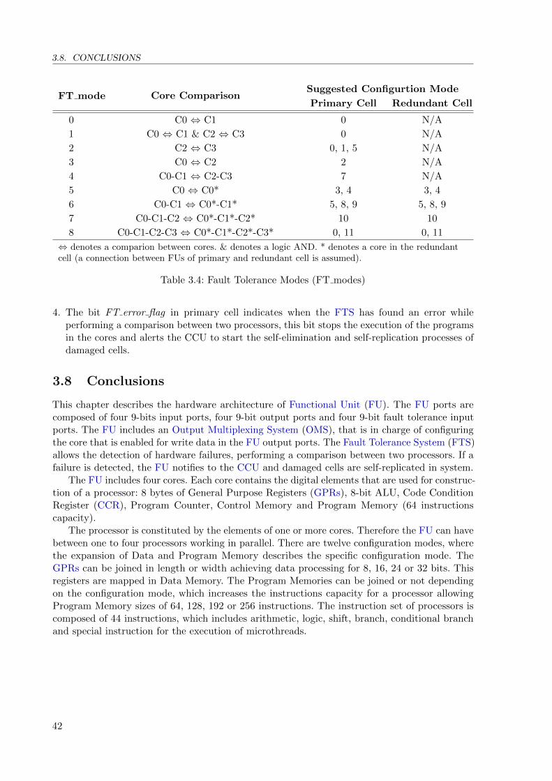
3.8. CONCLUSIONS
FT mode Core ComparisonSuggested Configurtion Mode
Primary Cell Redundant Cell
0 C0 ⇔ C1 0 N/A
1 C0 ⇔ C1 & C2 ⇔ C3 0 N/A
2 C2 ⇔ C3 0, 1, 5 N/A
3 C0 ⇔ C2 2 N/A
4 C0-C1 ⇔ C2-C3 7 N/A
5 C0 ⇔ C0* 3, 4 3, 4
6 C0-C1 ⇔ C0*-C1* 5, 8, 9 5, 8, 9
7 C0-C1-C2 ⇔ C0*-C1*-C2* 10 10
8 C0-C1-C2-C3 ⇔ C0*-C1*-C2*-C3* 0, 11 0, 11
⇔ denotes a comparion between cores. & denotes a logic AND. * denotes a core in the redundantcell (a connection between FUs of primary and redundant cell is assumed).
Table 3.4: Fault Tolerance Modes (FT modes)
4. The bit FT error flag in primary cell indicates when the FTS has found an error whileperforming a comparison between two processors, this bit stops the execution of the programsin the cores and alerts the CCU to start the self-elimination and self-replication processes ofdamaged cells.
3.8 Conclusions
This chapter describes the hardware architecture of Functional Unit (FU). The FU ports arecomposed of four 9-bits input ports, four 9-bit output ports and four 9-bit fault tolerance inputports. The FU includes an Output Multiplexing System (OMS), that is in charge of configuringthe core that is enabled for write data in the FU output ports. The Fault Tolerance System (FTS)allows the detection of hardware failures, performing a comparison between two processors. If afailure is detected, the FU notifies to the CCU and damaged cells are self-replicated in system.
The FU includes four cores. Each core contains the digital elements that are used for construc-tion of a processor: 8 bytes of General Purpose Registers (GPRs), 8-bit ALU, Code ConditionRegister (CCR), Program Counter, Control Memory and Program Memory (64 instructionscapacity).
The processor is constituted by the elements of one or more cores. Therefore the FU can havebetween one to four processors working in parallel. There are twelve configuration modes, wherethe expansion of Data and Program Memory describes the specific configuration mode. TheGPRs can be joined in length or width achieving data processing for 8, 16, 24 or 32 bits. Thisregisters are mapped in Data Memory. The Program Memories can be joined or not dependingon the configuration mode, which increases the instructions capacity for a processor allowingProgram Memory sizes of 64, 128, 192 or 256 instructions. The instruction set of processors iscomposed of 44 instructions, which includes arithmetic, logic, shift, branch, conditional branchand special instruction for the execution of microthreads.
42

Chapter 4
Self-Adaptive Processes
If you want to run, run a mile. If you want toexperience a different life, run a marathon.
Si quieres correr, corre una milla. Si quieresexperimentar una vida diferente, corre un maraton.
Emil Zatopek (1922 – 2000)
Abstract: This chapter describes the self-adaptive capabilities included in the architecture,
mainly the self-placement and self-routing, which due to its intrinsic design, enable the
development of systems with runtime self-configuration, self-repair and/or fault tolerance
capabilities. The self-adaptive capabilities are executed in an autonomous and distributed
way by Configuration Units of Cells, Switch and Pin Interconnection Matrices.
4.1 Summary
The following is a summary of the self-adaptive processes that are supported by the architecturepresented in this document, which will be explained in detail along this chapter. Note that mostof the self-adaptive capabilities are based in self-placement and self-routing processes.
1. Self-placement: it is responsible for finding out the most suitable position in the cell arrayto insert the new cell of a component. This process is divided in two:
I Self-placement for the first cell of a component.I Self-placement for other cells of a component.
2. Self-routing: it allows interconnecting the FU ports of two cells. The interconnection of cellscan be at two levels:
I Cell level, through local and remote cell ports.I Component level, through Switch and Pin Interconnection Matrices.
When a connection between cells must be eliminated, the Self-derouting process permits todisconnect the FU ports of two cells (at cell and component level), i.e., it releases the routingresources of a connection.
3. Self-replication: it permits to replicate the cell of a component to an empty cell in the array.For this purpose, the process includes the execution of the following processes for a specificcell in the order listed: self-derouting, self-placement and self-routing.
43

4.2. PREVIOUS CONSIDERATIONS
4. Self-elimination: it permits to eliminate and discard a specific cell(s) for future self-placementprocess when a hardware failure is detected. Its routing resources continue available and itcan participate in future self-routing processes.
5. Self-configuration: it includes all previous self-adaptive process listed, and could be dividedin two scenarios:
I Self-repair: when the Static Fault Tolerance mechanism is enabled and a hardware failureis detected, the processes for self-replication and self-elimination of damaged cell(s) areexecuted.
I Dynamic reconfiguration: when the execution of subprocesses is enabled for a component.It has the ability of create and eliminate components, among others. Therefore, the self-placement and self-routing processes could be executed.
4.2 Previous Considerations
For the understanding of the proposed algorithms, it is important to note that the ControlMicroprocessor (CµP) includes the high-level instructions in system, which will be executedsequentially for the configuration of a SANE-ASM. These high-level instructions will be definedas SANE Assembler (SASM) instructions.
This is the starting point for the configuration of an application in the system. The SASMinstructions will be detailed in chapter 5. In advance, for the understanding of the followingsections some SASM instructions are introduced:
I create component.I connect component.I delete component.I start subprocess X.I end subprocess X.I ft configuration (Fault Tolerance configuration).
The name of each SASM instruction gives an idea of its functionality. The execution of thisinstructions may require a negotiation process to establish the chip that has to execute a specificprocess. Once the chip is defined, the CµP sends the information to the Global ConfigurationUnit (GCU) of the selected chip to execute the desired action. Thereby, the GCU is the startpoint for the execution of self-placement and self-routing algorithms inside a chip. When theprocesses end, the GCU receives a confirmation command and notifies to the CµP the end ofthe process. Thereafter, the CµP may continue with the execution of other SASM instructions.The communication between Configuration Units (CUs), GCU and CµP is made through theInternal Network (INET) and the External Network (ENET). The labels “ inet” and “ enet”will be added to the commands related with these networks along this chapter.
It is important to note, that the algorithms presented in this chapter are being executed byseveral CUs at the same time in distributed way. Therefore, each CU includes its proper set ofvariables, e.g., the result of the execution of the algorithms is independent for each cell. Theflow diagrams for self-adaptive algorithms in cells and Switch Matrices (SMs) are summarizedin Appendix C and will be introduced along this chapter.
4.3 Initial State, Cell Address and Connection Tables
In the initial state, all cells are free, i.e., they do not belong to any component. The cells belongingto any component have to be placed and connected for data processing and information exchange.
44

CHAPTER 4. SELF-ADAPTIVE PROCESSES
FU
AAAA0002
BBBB0001
FUFU
AAAA0001
CCCC0001
32-bitggAddress
16-bitggid_component 16-bitggid_cell
A A A A 0 0 0 1
InputsgConnectiongTableg-gCellgAAAA0001
SourcegPort TargetgPort SourcegCellNIN0OUT01 BBBB0001IN1OUT12 BBBB0001IN2OUT23 BBBB0001IN3OUT34 BBBB0001
FT_IN0OUT05 AAAA0002FT_IN1OUT16 AAAA0002FT_IN2OUT27 AAAA0002FT_IN3OUT38 AAAA0002
OutputsgConnectiongTableg-gCellgAAAA0001
SourcegPort TargetgPort TargetgCellNIN0OUT01 BBBB0001IN1OUT1 BBBB0001IN2OUT2 BBBB0001IN3OUT3 BBBB0001IN3OUT0 CCCC0001IN2OUT1 CCCC0001IN1OUT2 CCCC0001IN0OUT3 CCCC0001XX 00000000
XX 00000000
23456789
20
FUIN0IN1IN2IN3
OUT0OUT1OUT2OUT3
FT_IN0FT_IN1FT_IN2FT_IN3
FU
Figure 4.1: Address and Connection Tables example for cell AAAA0001.
This is a sequential process where each cell has to be placed and routed in the system. For thispurpose, the cells execute in a distributed way the self-placement and self-routing algorithms.
All cells have a 32-bit unique identifier called address. This field is divided into two 16-bitwords, called id component and id cell . The id component is the component unique identifier,where the value FFFFh is reserved for broadcasting and the value 0000h to indicate that the cellis free and does not belong to any component (initial value). Therefore, it is possible to instantiateup to 65534 different components. The id cell is the cell unique identifier in a component, sothere may be up to 65536 cells in a component and a maximum close to 232 cells in the system.
All cells has two connection tables as detailed below:
I The Input Connection Table store the connections of the eight inputs of FU (includingthe fault tolerance input ports). This table includes the fields source port, target port andsource cell, which corresponds to a connection between the FU output port of another cellwith the FU input of the cell.
I The Output Connection Table can store up to 20 connections, which is limited for thenumber of port of the cell, i.e., 8 local ports plus 12 remote ports. When the cell includesconnections with other components, the number of connections within the same componentsis proportionally reduced. This table includes the fields source port, target port and targetcell, which corresponds to a connection between the FU output port of the cell with the FUinput port of another cell.
Figure 4.1 shows an example of the address and connection tables for the cell AAAA0001 in aSANE with three components.
4.4 Creation of Components in a Chip
The create component and connect component are basic instructions that permit the system tocreate and interconnect new components in the cell array. These SASM instructions require theexecution of two basic self-adaptive processes: self-placement and self-routing. These algorithmsare executed in an autonomous and distributed way by system members (cells, SMs and PIMs).The Cell Configuration Unit (CCU) includes the algorithms for all self-adaptive processes atcell level. It includes an interface with the INET that implements the respective communicationprotocol (see sections 2.11 and 2.12 for details). The Switch Matrix Configuration Unit (SMCU)and Pin Interconnection Matrix Configuration Unit (PIMCU) include the algorithms for self-routing at component level.
45

4.5. SELF-PLACEMENT PROCESS
6
3
6
66
3
3
3
3
3
3
3
3 3 3 3
3 3 3 3
0 0 0
0 0 0 0
0 0 0 0
0 0 0 0
1
0 1
1
1
2 2
22
2
2
3
3
3
3
3
3
4
4
4
4
4
4
4
5 5
5
5
5
5
6
6
6
7
7 8
Distance
10
0
5
5 2
2
4
4
4
6
6
6
6
7
7
8
8
8
9
9
10
10
11
11
11
11
12
13
1316 15 17
17
16
15
22
Congestion Affinity = 2·Distance + Congestion
2
Busy neighbor cells
(a) (b) (c) (d)
2
22
1 1 1 1
1 1 1 1
1
1
1
1
1
1
1
1
0
0
0
0
0
0
0
0
0
0
0
0
0
0
0 00
Figure 4.2: Example of busy neighbor cells, congestion, distance and affinity .
In addition to the communication functionality, the transmission (tx) and mainly the reception(rx) processes participate actively in the self-routing and self-placement algorithms. It is importantto note that tx and rx processes can be executed simultaneously by one or more cells in thearray, even the rx process can modify the data of the tx process if it is necessary, e.g., for thecomparison byte and the acknowledgment bit. The flow diagram for tx and rx processes is shownin Section C.1.
4.5 Self-Placement Process
The self-placement algorithm is responsible for finding out the most suitable position in the cellarray to insert the new cell of a component. For the placement of components in the array itis advisable but not essential to have the cells organized by number of connections with othercells. Therefore, the cell with more connections is first placed in a convenient place, where thereis a large number of free neighboring cells. The following variables are defined for self-placementprocess:
I Busy neighbor cells: This value indicates the number of busy cells around a cell. The cellsin the border of the array includes busy (or not implemented) cells by default.
I Congestion: The routing congestion figure (4.1) is defined as the number of remote outputports that are busy (or not available) in a cell. The cells in the border of the array includebusy (or not implemented) remote ports by default.
congestion = remote ports used (4.1)
I Distance: The distance between two cells is the sum of the absolute differences of theircoordinates (Manhattan distance).
I Affinity: The figure cost affinity indicates the location appropriateness for the placement ofthe new cell of a component with respect to another cell of the same component. The affinityis defined in (4.2).
affinity = 2 · distance+ congestion (4.2)
Figure 4.2 shows an example of these variables. It assumes the initial configuration, i.e., thereare no routing resources used. These variables are modified dynamically, each time that a cell isplaced or a connection is routed. Note that distance and affinity values are relative to a specificcell (highlighted).
46

CHAPTER 4. SELF-ADAPTIVE PROCESSES
4.5.1 Self-Placement of the First Cell of a Component
For the placement of the first cell of a component, a particular procedure is used, different fromother cells. In this case, a good candidate position is defined as one where a free cell has lowrouting congestion and the largest number of free neighboring cells. The procedure includes thenext steps:
1. The GCU broadcasts by means of the INET a message with the new cell identifier (address)and its input and output connection tables.
� tx command=insert first cell inet.� tx address=0xFFFFFFFF.� tx data = new cell address (4 bytes) + connection tables.
2. Free cells send simultaneously through INET, using a comparison process, the addition resultof the number of busy neighbor cells and congestion value ((a) + (b) in Figure 4.2).
3. The winner cell will be the leftmost uppermost cell with the lowest value. This cell stores theaddress and the connection tables. Additionally, it sends a message to the GCU indicatingthe end of the ”self-placement of the first cell of a component” process, e.g., the highlightedcell in Figure 4.2 shows the location of the first cell of a component, when the array is empty.
Section C.2.1 presents a flow diagram of the algorithm implemented by cells for the insertionprocess of the first cell of a component.
4.5.2 Self-Placement of Other Cells of a Component
After inserting the component first cell, the remaining cells of the component are placed as closeas possible to the cell with the largest number of connections with the new cell. For this purpose,the affinity is used. The procedure is as follows:
1. The GCU broadcasts to the cell array a message with the new cell identifier (address) andits connection tables.
� tx command=insert other cell inet.� tx address=0xFFFFFFFF.� tx data = new cell address (4 bytes) + connection tables.
2. The cells belonging to that component send a message by means of the INET indicatingthe one’s complement of the number of connections they share with the new cell, startinga comparison process. The winner cell will be the one which has the largest number ofconnections.
3. This cell starts a process, in which the distance with free cells is calculated. Then, it requeststo the free cells to start a comparison process of their affinity .
4. The winner cell will be the leftmost uppermost cell with the lowest affinity value. This cellstores the address and connection tables, e.g., the cell below the highlighted cell in Figure 4.2(d) corresponds to the second cell placed in the cell array.
Section C.2.2 presents the flow diagram of the algorithm that performs the self-placementof the other cells of the component (from the second). Figure 4.3 shows an example withthree components in an array of two clusters (6x3 cells array). This figure shows the executionsequence of self-placement and self-routing processes for component AAAA. The final locationof component BBBB and CCCC is also shown.
47

4.5. SELF-PLACEMENT PROCESS
C4B2 B1
A1
A2A5
A3
A5A6
A4
A4A3
A1
A2
A6A5
B3
B1
B4
B2
B7
B5
B6
C1
C1
C1
C1
Component AAAA Component BBBB Component CCCC
Placement order: A3, A4, A6, A5, A2, A1
Placement order: B4, B5, B3, B1, B2, B7, B6
Placement order: C4, C1, C2, C3
A3
A3 A4 A3 A4 A6
A2 A4 A6A3 A5
A1
A4 A6A3
A2 A5A4 A6A3
B7 B5 B4 B3
B6
B2 B1
A1
A2 A5A4 A6A3
B7 B5 B4 B3
B6
C3C2C1
1 2
3 4
5 6
7 8
Figure 4.3: Example of the self-placement algorithm implementation for three components in anarray of two clusters (6x3 cell array). The resources used by self-routing algorithm are shownonly for component AAAA.
48

CHAPTER 4. SELF-ADAPTIVE PROCESSES
4.6 Self-Routing Process
The Self-routing allows interconnecting the FU ports of two cells. It can be at cell level, throughthe local and remote cell ports, or at component level, through the Switch Matrices (SMs) andPin Interconnection Matrices (PIMs).
When a cell or a component must be deleted form the array, the self-routing process mustbe executed for disconnecting the FU port of cells previously connected. This process will bedefined as Self-derouting. This process can be at cell level or a component level.
Section C.3 and C.4 presents the flow diagrams of the Self-Routing processes implementedin CCUs and SMCUs respectively. The following section describes these processes.
4.7 Self-Routing at Cell Level
The self-routing algorithm at cell level is executed since the insertion of the second cell of acomponent, each time that the self-placement process ends. The algorithm allows interconnectingthe ports of the functional unit of two cells, in the same component, through the local and remotecell ports. The local input-output ports are used exclusively to interconnect the FU ports oftwo neighbor cells (north, east, south or west). The remote ports are used when the cells to beconnected are not adjacent or when the local ports are already occupied.
This process is divided in two parts. The first consists in locating the source and the targetcell inside the cell array for a specific connection. For this procedure, the INET is used. Thesecond is an expansion process between the source and target cells. This process is executed eachtime that the source and target cells are configured for a new connection. The cell multiplexersare dynamically configured to interconnect the desired ports. In this process, some bits of theexpansion ports are used (see section 2.10 for details).
4.7.1 Configuration of source and target cells for cell connections
The first cell that starts the self-routing process is the newly inserted cell, which activates itssource cell flag .
1. The source cell goes through its output connections table, and sends messages to cells of thesame component.
2. If the address of a busy cell that receives this message matches with the address of the message,this cell activates its target cell flag and sets the acknowledge signal to the source cell . Then,the source cell starts the “Expansion Process at Cell Level” to configure the path.
3. If the source cell does not receive the acknowledge signal, it will continue with its remainingconnections.
4. When the source cell (new inserted cell) ends with its output connections table, it broadcastsa message including its address, asking for cells in the component able to route their outputconnections with this cell. Then, it resets its source cell flag and activates its target cell flag .
Hitherto, the new inserted cell tried to route all its output connections, which depends ofthe cells already placed. The output connections that has not been routed, will be made later,when cells that are inserted later complete the whole process. The algorithm continues with therouting of the input ports of the new inserted cell.
5. The cells of the component that have at least one output connection to be routed to thetarget cell start an elimination process, where the winner is the leftmost uppermost cell.
49

4.7. SELF-ROUTING AT CELL LEVEL
Signal name Description
neighbor out X Used in the Search Phase. These signals are used to find the target cellin neighboring cells.neighbor in X
propagate out X Used in the Search Phase. These signals are used to find the target cellin the cell array.propagate in X
lock out X Used in the Configuration Phase. These signals are used in the reverseprocess of the Search Phase, to configure the multiplexers in the cellsincluded in the path.
lock in X
local port out XUsed in both phases, the Search and Configuration. These signals areused to indicate the local or remote port that will be used in case toconfigure the path.
local port in X
remote port out X
remote port in X
id target port out Used in the Search Phase. These signals are used to indicate theconnection target port of the target cell .id target port in X
Table 4.1: Description of expansion port signals used by the Expansion Process at Cell Level.
6. The winner cell activates its source cell flag . This new source cell looks up its output connec-tions table and starts the “Expansion Process at Cell Level” to configure all connection pathsbetween source and target cells.
7. When the source cell ends routing all possible connections with the target cell , it broadcastsa message asking for other cells in the component able to make their output connections withthe target cell .
8. Steps 5., 6. and 7. are repeated until all connections are completed with the target cell . Whenthe process ends, the last source cell sends a message to the GCU indicating the end ofself-routing and self-placement process for the inserted cell.
Section C.3.1 shows the algorithm used for the selection of source and target cells. When thiscells are selected, the “Expansion Process at Cell Level” can be executed. The total time of theself-placement and self-routing processes of the new inserted cell depends on some factors, likethe placement order and the component interconnections that includes the number of connectionsbetween cells (inputs and outputs).
4.7.2 Expansion Process at Cell Level
Once the source and target cells of a component are ready, the expansion process starts, config-uring the cell multiplexers to interconnect the FU ports between those cells. The signals thatparticipate in this process are explained in Table 4.1.
When a cell has to be connected to another one, the system first checks if the cells areneighbors. In that case, and if a free local port exists between them, they get connected by meansof the local ports, otherwise the connection is tried with a remote connection resource.
The path configuration is divided in two phases. The first one is the Search Phase at CellLevel. This starts from the source cell and looks for the target cell in the array. During theprocess some information is stored, in a distributed way, in every cell that has been visited. Thephase ends when the target cell has been found. If the first phase exhausted any possibility tofind the target cell without reaching it, then no path exists between the source cell and the
50

CHAPTER 4. SELF-ADAPTIVE PROCESSES
target cell , and there is no reason to continue with the second phase. Then, the source cell sendsan error message to the GCU and the self-routing process ends.
The second phase recovers the information generated by the first one for the path configuration.This is called the Configuration Phase at Cell Level, it starts from the target cell to thesource cell using the propagation information stored during the first phase of the algorithm.
Sections C.3.2, C.3.3 and C.3.4 presents the flow diagrams related with the expansion processat cell level.
Search Phase at Cell Level
The Search Phase is started by the source cell . This is an expansion process that propagatessignals in the sides of the cell that have available routing resources, like local and/or remote freeports. The propagation process includes the configuration of signals for each side (north, east,south and west) of the cell as follows:
a Configuration of propagation signals:
I This condition is valid only for the source cell : If the side of the cell has any free localport, then that side sets the neighbor out signal and configures the local port id out signalin the expansion port.
I For propagation of any cell (including the source cell): If the side of the cell has any freeremote port, then that side sets the propagate out signal and configures the remote portid out signal in the expansion port.
b The cell assigns to the signal id target port out the value:
I For source cell , the identification number of the Functional Unit target port for the con-nection with the target cell . This number is read from the output connections table of thesource cell .
I For other cells, the signal id target port in read from the port that receives the propagationsignal.
c After the configuration of the signals previously mentioned, the cell goes to the state lockcell, where it waits for the activation of any lock in signal.
The propagation previously explained is executed by each cell that reads the propagatein signal. When a cell receives more than one propagate in signal simultaneously it follows apriority order (NORTH, EAST, SOUTH and WEST) and it serves only the highest priority signalreceived. The cell receiving the propagate in signal stores the side from which the expandingcell accessed it by means of the origin register. The propagation process explores the entire cellarray until finding the target cell , if possible.
It is important to mention that busy cells also participate in the expansion process since theremote connections can also cross busy cells. Nevertheless, this process is completely transparentto the internal cell operation since it is executed using dedicated resources, at the placement androuting layer.
Configuration Phase at Cell Level
The Configuration Phase starts when the Search Phase finds the target cell . This occurs whenany propagation signal in any side of the target cell is activated, then the target cell proceeds inpriority order as follows:
51

4.7. SELF-ROUTING AT CELL LEVEL
SOURCE
TARGET
SOURCESOURCE
TARGET TARGET
SOURCE
TARGET
SOURCE
TARGET
SOURCE
TARGET
SOURCE
TARGET
SOURCE
TARGET
SOURCE
TARGET
SOURCE
TARGET
SOURCE
TARGET
1 2 3
4 5
6 7 8
9 10 11
ExpansiongProcessgatgCellgLevel
Stepsg1gtog5:gSearchgPhase
Stepsg6gtog11:ConfigurationgPhase
Figure 4.4: Example of Expansion Process at Cell Level.
1. If the target cell detects in any of its sides the activation of a neighbor in signal, it will knowthat the source cell is its neighbor and also its position (If not, go to step 2.). At that moment,the local connection is established. The connection is configured taking into account thesignals id target port in and local port id in. Then the cell activates the signal lock out andneighbor out in the side where the neighbor in signal was received, and it goes to idle state.
2. If the target cell detects in any of its sides the activation of a propagate in signal, it willknow its position. At that moment, the remote connection is established. The connection isconfigured taking into account the signals id target port in and remote port id in. Then thecell activates the signal lock out in the side where the propagate in signal was received, andgoes to idle state.
The Configuration Phase that was started by the target cell goes backward over the pathpreviously configured in the Search Phase until it arrives to the source cell . This process configuresthe multiplexers of the corresponding cells to fix the path. The cells that participate in thisprocess are in the state lock cell and perform the following actions when the signal lock in inthe corresponding side is activated:
1. If it is the source cell : the cell configures the local or remote port taking into account thesource port of the Functional Unit included in the connection table and the signal local portid or remote port id previously configured. The local port is used if the signal neighbor in isactive. The cell activates the signal routing complete (shared by all the cells) in order to reset
52
CHAPTER 4. SELF-ADAPTIVE PROCESSES
all the signals related to the expansion process, and the Expansion Process for a connectionends.
2. If it is not the source cell: the cell configures the remote port of the side where the lockin signal was read taking into account the origin register and the remote port id previouslyconfigured. The cell goes to idle state and the signal lock out is activated in the side thatindicates the register origin.
3. The next cell that receives the signal lock in starts the process again from step 1.
Figure 4.4 shows an example of the Search and Configuration Phases of the Expansion Processat Cell Level. This example assumes that routing resources of all cells are available. Step 1 to 5represents the Search Phase, that starts from the source cell propagating signals until it findsthe target cell , then the Configuration Phase starts (steps 6 to 11). Note that the propagation ofsignals continue in steps 6 and 7, since the Expansion Process is finalized by source cell in step11. Note that the distance between source cell and target cell is 5, the connection is establishedthrough six routing resources (or multiplexers), five in remote port of cells and one in FU inputof target cell , this resources are represented with the head of the arrows in step 11.
Figure 4.3 shows a sequence that illustrate the execution of self-placement and self-routingalgorithms for the component AAAA (steps 1 to 6). Note that a connection can cross a free cell(step 5). Equation (4.3) represents the execution time of the expansion process implemented forthe prototype. This time is proportional to the distance between cells and the clock period, T .
TEP = (4 · distance+ 2)T (4.3)
4.8 Self-Routing at Component Level
When the creation of all components in system is completed, the self-routing process at componentlevel can be executed by means of the SASM instruction connect component. This algorithmimplements the interconnection of cells belonging to different components through SMs (andPIMs if chip-to-chip connection is necessary).
The process is divided into two parts, the first configures the source and target cells of aconnection between different components, and the second is the “Expansion Process at Compo-nent Level” that is performed through the SMs, where the Switch Matrix Configuration Unit(SMCU) and eventually Pin Interconnection Matrix Configuration Unit (PIMCU) are responsibleof the configuration of the multiplexers to connect the desired ports. The interconnection ofcomponents can be done in the same cluster or in different clusters. In the latter case the SMwill be interconnected with one of its eight neighbors and so on, until reaching the target cell ofthe connection.
The self-routing process at component level is similar to the self-routing process at cell levelpreviously described. The process is started and completed by the cells with the difference thatthe expansion process is performed in the Switching Matrices, using a similar algorithm that isused by cells in the expansion process. The main difference is that matrices have eight neighbors,while cells have only four. This allows interconnecting distant cells using less routing resources(multiplexers) in comparison with routing hardware resources for cells.
If in the search process of the target cell the acknowledge signal is not received, it may bebecause the target cell is in another chip. In this case, the pins through which the connectionbetween source and target will be made are configured by the GCUs of the corresponding chips,initiating self-routing processes at the component level in the chips through which the connectiongoes through. This process will involve the PIMCU–in addition to the SMCUs– configuring themultiplexers required to perform the desired connection.
53

4.8. SELF-ROUTING AT COMPONENT LEVEL
4.8.1 Configuration of Source and Target Cells for Components Connections
The procedure is as follows:
1. The GCU of a chip starts the execution of the algorithm sending to the cell array the commandstart components connection inet.
2. All cells with at least one pending connection with a cell of other component participate inthe elimination process, where the leftmost uppermost is the winner cell. If there is a winnercell, it activates its source cell flag (goto step 3). If there is not a winner the GCU receivesthe command end components connection inet and the process ends.
3. The source cell looks up its output connections table. If there is a non-routed connectionwith a cell belonging to other component, the source cell sends a message to find the targetcell by means of command set target cell sr component inet (goto step 4). If there is no moreconnections to route goto step 2.
4. If the target cell of a connection is in the same chip, this cell activates its target cell flag andsets the acknowledge signal to the source cell . Then, the source cell starts the “ExpansionProcess at Component Level” to configure the path with the target cell , the process continuesin step 3. If the source cell does not receive the acknowledge signal, it is possible that thetarget cell is located in another chip. Then, the following additional steps must be executed:
a. The chip that contains the source cell is marked as source chip. The source cell sends tothe GCU the command configure chip connection inet for the configuration of a connectionbetween chips.
b. The GCU broadcasts to chips the command search cell other chip enet with the addressof the target cell and the FU target port of the connection.
c. The chips broadcast internally the information. The chip that contains the target cell ismarked as target chip. The target cell activates its target cell flag . The target chip selectsa free pin of its PIM and sends the information to the source chip.
d. The source chip starts the “Expansion Process at Component Level” between the sourcecell and the target pin of the PIM. When the process ends, the source cell sends to theGCU the confirmation command cell pin connection confirmation inet. The GCU sends tothe target chip the command routing cell target chip enet requesting the routing process.
e. The GCU of the target chip broadcasts internally the command start pin cell connectioninet. The target chip performs an ”Expansion Process at Component Level” between thesource pin of the PIM and the target cell . When the process ends, the PIM sends to theGCU the confirmation command pin cell connection confirmation inet.
f. The GCU of the target chip broadcasts the confirmation message end routing cell targetchip enet, later the GCUs broadcast internally the command configure chip connectionconfirmation inet.
g. The connection between source cell and target cell at component level using PIMs hasbeen performed, the source cell continues the process from step 3.
4.8.2 Expansion Process at Component Level
The expansion process at component level can be executed for three scenarios:
I Between source cell and target cell when the components belong to the same chip.
54

CHAPTER 4. SELF-ADAPTIVE PROCESSES
Signal name Description
propagate out matrix (cell)
Used in the Search Phase. These signals are used tofind the target cell or target pin in the chip.
propagate in matrix (cell)
propagate out cell X (SM)
propagate in cell X (SM)
propagate out X (SM, PIM)
propagate in X (SM, PIM)
lock out matrix (cell)
Used in the Configuration Phase. These signals are usedin the reverse process of the Search Phase, to configurethe multiplexers in the matrices included in the path.
lock in matrix (cell)
lock out cell X (SM)
lock in cell X (SM)
lock out X (SM, PIM)
lock in X (SM, PIM)
id source port out (cell) Used in the Search Phase. These signals are used toindicate the FU source port of a connection.id source port in X (SM)
mux id matrix (cell) Used when the Search Phase finds the target . Thesesignals are used to indicate the multiplexer used by SMfor configures a connection.
mux id cell X (SM)
matrix port out (SM, PIM) Used in both phases, the Search and Configuration.These signals are used to indicate the matrix port thatwill be used for the path configuration.
matrix port in (SM, PIM)
id target port out (cell, SM, PIM) Used in the search phase of the target cell. Thesesignals are used to indicate the FU target port of thetarget cell or the target pin of the PIM.
id target port in matrix (cell)
id target port in X (SM, PIM)
Table 4.2: Description of expansion port signals used by the Expansion Process at componentlevel.
I Between source cell and target pin when the components belongs to different chips (partialconfiguration of a connection).
I Between source pin and target cell when the components belongs to different chips (partialconfiguration of a connection).
For the description of the process, the term source may refer to source cell or source pin, whilstthe term target my refer to target cell or target pin. Once the source and target are ready, theexpansion process starts, configuring the multiplexers of SMs (and PIMs) for a connection. Thesignals that participate in this process are explained in Table 4.2.
The path configuration is divided in two phases. The first one is the Search Phase atComponent Level. This starts from the source and looks for the target in the chip. During theprocess some information is stored, in a distributed way, in every SM or PIM that has been visited.The phase ends when the target has been found. If the first phase exhausted any possibility tofind the target without reaching it, then no path exists between the source and the target , andthere is no reason to continue with the second phase. Then, the source sends an error messageto the GCU and the self-routing process ends.
The second phase recovers the information generated by the first one for the path configuration.This is called the Configuration Phase at Component Level, it starts from the target tothe source using the propagation information stored during the first phase of the algorithm.
55

4.8. SELF-ROUTING AT COMPONENT LEVEL
Sections C.3.2, C.4, C.4.1 and C.4.2 present the flow diagrams related with the expansionprocess at component level. Note that the source (CCU for presented flow diagrams) is the startand end point of the process.
Search Phase at Component Level
This is an expansion process that propagates signals in cells and the sides of the SMs or PIMsthat have available routing resources. The Search Phase is started by the source as follows:
a. If the source is a cell: the cell sets its propagation out matrix signal. The cell reads the FUsource port from output connections table and assigns the value to the signal id source portout. If the target cell is in the chip, the cell reads the FU target port from output connectionstable and assigns the value to the signal id target port out. If the target cell is in anotherchip, the cell reads the target pin from a previous configured value and assigns it to the signalid target port out
b. If the source is a PIM: whether the side of the PIM has any free output port, then that sidesets the propagate out signal. The PIM configures the id target port out that contains theFU target port from the data read in a previous configuration.
c. After the configuration of the signals previously mentioned, the cell or PIM goes to the statelock component, where it waits for the activation of any lock in signal.
The SM receiving the propagate in cell X signal stores the side from which the expandingcell accessed it by means of the origin cell register. Thereafter, the propagation process continuesconfiguring the propagation signals for SMs in each side (north, northeast, east, southeast, south,southwest, west and northwest) as follows:
d. If the side of the SM has any free port, then that side sets the propagate out signal.
e. The SM assigns to the signal id target port out the value read from the cell, SM or PIM,depending of the port that receives the propagation signal.
f. After the configuration of the signals previously mentioned, the SM goes to the state lockcomponents, where it waits for the activation of any lock in signal.
The propagation previously explained (from d.) is executed by each SM that reads thepropagate in signal. When a SM receives more than one propagate in signal simultaneously itfollows a priority order (NORTH, NORTHEAST, EAST, SOUTHEAST, SOUTH, SOUTHWEST,WEST and NORTHWEST) and it serves only the highest priority signal received. The SMreceiving the propagate in signal stores the side from which the expanding SM accessed it bymeans of the origin matrix register. The propagation process explores the entire chip until findingthe target , if possible.
Configuration Phase at Component Level
The Configuration Phase starts when the Search Phase finds the target . This occurs when anypropagation signal in any side of the target is activated, then the target proceeds as follows:
I If the target is a cell: when the target cell detects the activation of the signal propagate inmatrix, the connection with the SM is established. The connection is configured taking intoaccount the signals mux id matrix and id target port in matrix. Then the cell activates thesignal lock out matrix, and it goes to idle state.
56
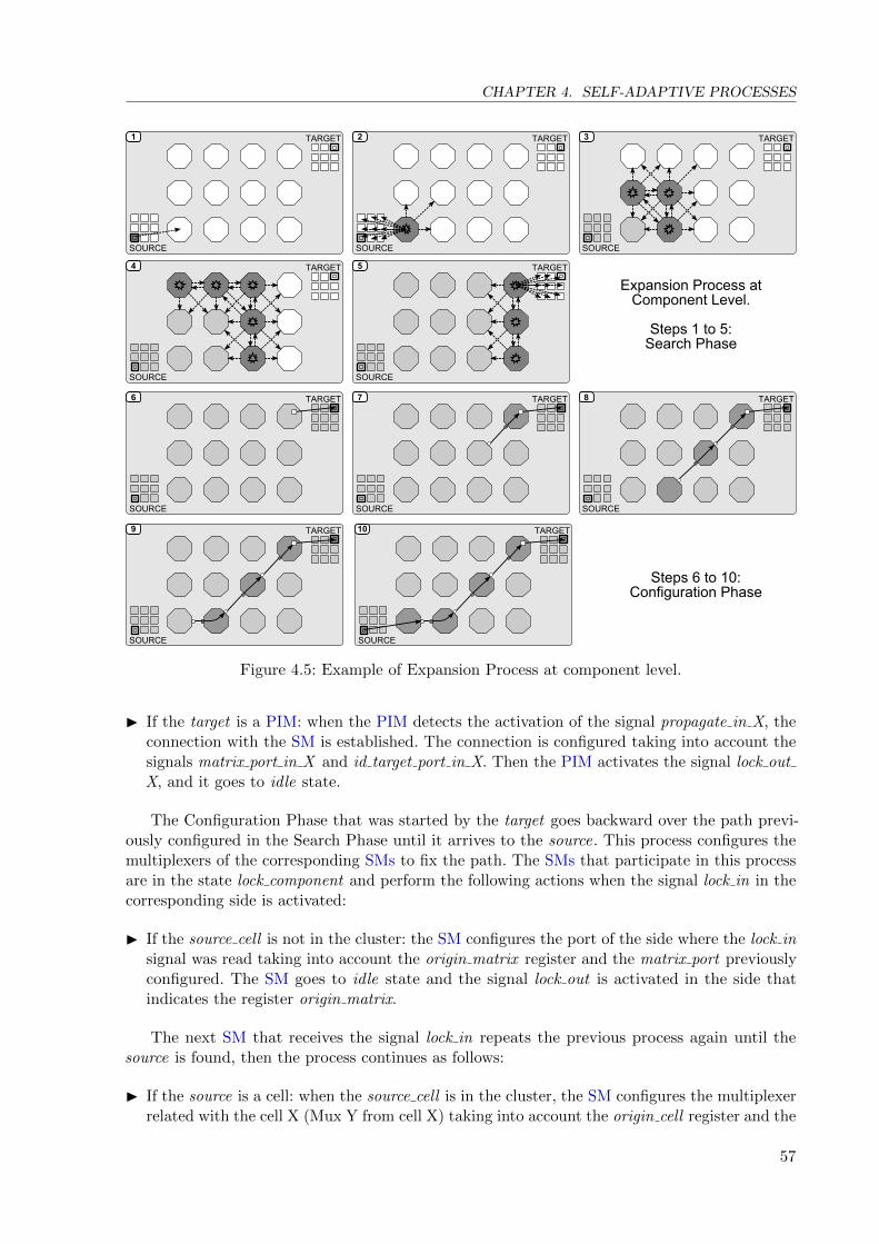
CHAPTER 4. SELF-ADAPTIVE PROCESSES
SOURCE
TARGET1
SOURCE
TARGET2
SOURCE
TARGET3
SOURCE
TARGET4
SOURCE
TARGET5
SOURCE
TARGET6
SOURCE
TARGET7
SOURCE
TARGET8
SOURCE
TARGET9
SOURCE
TARGET10
Expansion6Process6atComponent6Level.
Steps616to65:Search6Phase
Steps666to610:Configuration6Phase
Figure 4.5: Example of Expansion Process at component level.
I If the target is a PIM: when the PIM detects the activation of the signal propagate in X, theconnection with the SM is established. The connection is configured taking into account thesignals matrix port in X and id target port in X. Then the PIM activates the signal lock outX, and it goes to idle state.
The Configuration Phase that was started by the target goes backward over the path previ-ously configured in the Search Phase until it arrives to the source. This process configures themultiplexers of the corresponding SMs to fix the path. The SMs that participate in this processare in the state lock component and perform the following actions when the signal lock in in thecorresponding side is activated:
I If the source cell is not in the cluster: the SM configures the port of the side where the lock insignal was read taking into account the origin matrix register and the matrix port previouslyconfigured. The SM goes to idle state and the signal lock out is activated in the side thatindicates the register origin matrix.
The next SM that receives the signal lock in repeats the previous process again until thesource is found, then the process continues as follows:
I If the source is a cell: when the source cell is in the cluster, the SM configures the multiplexerrelated with the cell X (Mux Y from cell X) taking into account the origin cell register and the
57

4.9. SELF-ELIMINATION AND SELF-REPLICATION
signals id source port in X and matrix port in X previously configured. The SM activates thesignal lock out cell X and it goes to the idle state. Thereafter, the cell that receives the signallock in matrix activates the signal routing complete (shared by all CUs), and the “ExpansionProcess at Component Level” ends.
I If the source is a PIM (it includes the source pin): the PIM configures the port taking intoaccount the signals id source port in X and matrix port in X previously configured. There-after, the PIM activates the signal routing complete (shared by all CUs), and the “ExpansionProcess at Component Level” ends.
Figure 4.5 shows an example of the Search and Configuration Phases of the Expansion Processat Component Level. This example assumes that routing resources of all SMs are available. Step1 to 5 represents the Search Phase, that starts from the source cell propagating signals untilfinds the target cell , then the Configuration phase starts (steps 6 to 10). Note that the distancebetween source cell and target cell is 19, however the connection is established through five routingresources (or multiplexers), four in SMs and one in target cell , this resources are representedwith the head of the arrows in step 10.
4.9 Self-Elimination and Self-Replication
The Static Fault Tolerance mechanism included in the system may require the execution ofprocesses for elimination and replication of cells. This mechanism is a combination between theFault Tolerance System (FTS) and the SASM instruction ft configuration, which is used forconfiguring the cell or cells involved in the process. Note that previous to the elimination of acell, all its connections must be derouted as detailed in section 4.11.
When a hardware failure is detected by the FTS, the damaged cell(s) request to the CµP toexecute the processes for self-eliminate and self-replicate the cell (or cells) involved in the failure.The SASM instruction ft configuration executes the process as detailed in section 5.3.8. Thecell data registers and its processing capacity is lost (probably corrupted). However, the routingresources and some adaptive capabilities of the cell (included in the CCU) are still working. Thisis due to routing resources of cell are independent of processing capabilities of cell, where thefailure was detected. This means that the cell continues participating in the self-placement (asbusy cell) and self-routing processes. This allows the interconnection of two distant cells in acomponent using the routing resources of a cell with damage in its FU.
4.9.1 Elimination of a Cell inside a Chip
The elimination of a cell is executed when the GCU sends the command eliminate cell inet. Then,the cell whose address matches with the address of frame executes the following actions:
1. Deletes the input and output connection tables.2. Disables FU processors.3. Deletes FU Program Memories.4. Sets the cell as busy. Therefore, the cell will not participate in future self-placement process.5. Sets the address as 0xFFFF0001. This is a special reserved address used for identification of
cells that have been eliminated by the Static Fault Tolerance mechanism.
Subsequently, the cell sends the confirmation command eliminate cell confirmation inet andthe process ends.
58

CHAPTER 4. SELF-ADAPTIVE PROCESSES
4.10 Self-Configuration by means of Subprocesses
Any SANE application can be assumed to be a self-adaptive processing system with the MIMDarchitecture advantages, like multiple parallel processing [7]. The runtime self-configurationcapability of the system is present when a SANE application requests the execution of at leastone subprocess.
Any component in the system has the ability to start up to four subprocesses in executiontime. The SASM instructions start subprocess X and end subprocess X are used for this pur-pose. Each subprocess may includes others SASM instructions like create component, connectcomponent and delete component among others, i.e., a subprocess could create, interconnector delete components between others.
The creation and interconnection of components are capabilities that has been described inprevious sections. The delete component capability will be detailed in the following section. Notethat before deleting a component, all its connections must be derouted as detailed in section 4.11.
4.10.1 Delete a Component inside a Chip
The runtime Self-configuration mechanism included in the system may require to start a processfor deleting components. The deletion of a component is executed when the GCU sends thecommand delete component chip inet. Then, the cells whose id component matches with the idcomponent included in the command execute the following actions:
1. Deletes the input and output connection tables.2. Disables FU processors.3. Deletes FU Program Memories.4. Sets the cell as free. Therefore, the cell can participate in future self-placement process.5. Sets the address as 0x00000000. This is a special reserved address used for identification of
free cells.
Subsequently, the cells send the confirmation command delete component confirmation inetand the process ends. Note that when a component is deleted, the cells that belonged to thecomponent can participate in future self-placement and self-routing processes. The routingresources of cells that will be deleted in this process are not altered, i.e, if a connection betweentwo cells crosses a cell that will be deleted, the connection remains configured after cell deletion.
4.11 Self-Derouting Process
The Self-derouting process permits to release all routing resources used to interconnect cells.This process can be executed for a single cell or a entire component. For cells, the process isexecuted taking into account the address of a specific cell (cell X ). For components, the processrequires the identification of a component (component X ).
The self-derouting algorithm for a single cell is executed by the Static Fault Tolerancemechanism, before starting the processes for eliminating and replicating cells. The cell thatwill be eliminated is the cell X . The algorithm permits to release all routing resources used tointerconnect the cell X , i.e., it permits to disconnect the cell X .
The self-derouting algorithm for a entire component is executed when a component willbe deleted, this is normally used by the runtime self-configuration mechanism by means ofsubprocesses in the high-level configuration file. The component that will be deleted is thecomponent X . The algorithm permits to release all routing resources used to interconnect thecomponent X , i.e., it allows to disconnect the component X .
59

4.11. SELF-DEROUTING PROCESS
This process is divided in two parts. The first consists in locating the cells that have at leastone connection with the cell X or with the component X . For this procedure, the INET is used.The second is the Release Process between the interconnected cells, i.e., the source and target ofa connection. This process is executed for each connection with the cell X or the component X .
Unlike the expansion processes at cell or component level, the Release Process has only onephase, that goes from the target to the source of a connection. When a connection betweencomponents uses PIMs, the source of a connection can be a source cell or a source pin, whilstthe target can be a target cell or a target pin. The Release Process is the same for target cell ortarget pin.
Sections C.3.2, C.3.5 and C.4.3 present the flow diagrams related with the release processesat cell and component level. Note that the CCU in the target cell and CCU in the source cell(for presented flow diagrams) are the start and end point of the process respectively.
4.11.1 Cell Selection for Derouting Process of a Single Cell
The process is described below:
1. The GCU starts the self-derouting process sending the command delete cell connections chipinet with the address of cell X as argument.
2. The cells look up their input connections table. The cell X and the cells that have at leastone input connection with the cell X participate in an elimination process, where the leftmostuppermost cell will be the winner, which will be the target for the Release Process. If there isnot a winner cell, there are no more connections with cell X , the process ends and the GCUreceives the command delete cell connections confirmation inet.
3. The winner cell (target) starts the “Release Process” for disconnecting all its input connectionswith the cell X . If the winner is the cell X , this starts the “Release Process” for disconnectingall its inputs connections with other cells.
4. When the winner cell ends looking up its inputs connections table, this sends the commanddelete cell connections chip inet with the address of cell X as argument and the process isrepeated again from step 2.
4.11.2 Cell Selection for Derouting Process of a Entire Component
The process is described below:
1. The GCU starts the self-derouting process sending the command delete components connectionschip inet with the identifier of component X as argument (id component).
2. The cells look up their input connections table. The cells that belongs to the component X ,and the cells that have at least one input connection with the component X participates in anelimination process, where the leftmost uppermost cell will be the winner, which will be thetarget for the “Release Process”. If there is not a winner cell, there are no more connectionswith component X , the process ends and the GCU receives the command delete componentsconnections confirmation inet.
3. The winner cell (target) starts the “Release Process” for disconnecting all its input connectionswith the component X . If the winner cell belongs to the component X , this starts the “ReleaseProcess” for disconnecting all its inputs.
60

CHAPTER 4. SELF-ADAPTIVE PROCESSES
TARGETTARGETTARGET
321
TARGET
4
TARGET
5
TARGET
6
TARGET1 TARGET2 TARGET3
TARGET4 TARGET5 TARGET6
SOURCE SOURCE SOURCE
SOURCESOURCESOURCE
SOURCE SOURCE SOURCE
SOURCESOURCESOURCE
Figure 4.6: Example of Release Process at Cell and Component Level.
4. When the winner cell ends looking its input connections table, this sends the commanddelete component connections chip inet with the identifier of component X as argument (idcomponent) and the process is repeated again from step 2.
4.11.3 Release Process
This process releases the routing resources used for a interconnection between cells, or between acell and a PIM. In this process, the multiplexers of cells, SMs and PIMs are dynamically releasedto disconnect the desired ports. If the connection is at cell level, the multiplexers of FU inputs,local and remote cell ports are released. If the connection is at component level, the multiplexersof FU inputs, SMs and PIMs are released. Figure 4.6 shows an example of the Release Processat cell and component level.
For this process some bits of the expansion ports are used (see section 2.10 for details). Thesignals that participate in this process are explained in Table 4.3.
The Release Process has only one phase, that goes from the target to the source of a connection.When a connection between components use PIMs, the source of a connection could be a sourcecell or a source pin, whilst the target could be a target cell or a target pin. The Release Process isthe same for target cell or target pin, so the following procedures assume the source and target ascells. Once the FU input port of the target cell is selected, the release process starts, configuringthe multiplexers to their initial state.
61

4.11. SELF-DEROUTING PROCESS
Signal name Description
del connection out X (cell, SM)Used to indicate the port that must be released. Thesignal used is propagated only in one side of the cell orSM.
del connection out cell X
del connection out matrix
del connection out cell
neighbor out XUsed to indicate that the connection is with a local port.
neighbor in X
local port out X
Used to indicate the local or remote cell port that wasused to configure the path.
local port in X
remote port out X
remote port in X
matrix port out X Used to indicate the SM port that was used to configurethe path.matrix port in X
id source port out Used to indicate to SM the FU input port that was usedto configure the path.id source port in X
Table 4.3: Description of expansion port signals used by the Release Process.
The Release Process starts from the FU input port of the target cell an go backwards tothe origin of a connection, i.e., the FU output port of the source cell . This process reads themultiplexers configuration and propagate the signal del connection out X in the direction wherethe connection was previously established by Expansion Process. The process is described bellow:
1 The target cell reads the configuration of the FU input port multiplexer selected for the ReleaseProcess and performs one of the following actions:
I If the FU input port is connected to a local port, the target cell propagates the signal delconnection out X in the side where the connection was established. It also propagates thesignals neighbor out X and local port out X that permits to the neighboring cell to identifythe local port used for a connection.
I If the FU input port is connected to a remote port, the target cell propagates the signaldel connection out X in the side where the connection was established. It also propagatesthe signal remote port out X that permits to the neighboring cell to identify the remoteport used for a connection.
I If the FU input port is connected to SM, the target cell propagates the signal del connectionout matrix. It also propagates the signal id source port out that permits to the matrix toidentify the multiplexer used for a connection.
2 The target cell releases the FU input port multiplexer, and goes to idle state.
3 The process continues at cell level or component level as follows:
a. At cell level: when a cell receives the signal del connection in X proceeds as follows:
i. If the signal neighbor in X is received: it confirms that this cell is the origin of aconnection, the local port multiplexer is released and the process ends.
ii. If the remote port is connected to a FU output port of the cell: it confirms that thiscell is the origin of a connection, the remote port multiplexer is released and theprocess ends.
62

CHAPTER 4. SELF-ADAPTIVE PROCESSES
iii. If the remote port is connected to another remote port: the cell propagates thesignal del connection out X in the side where the connection was established. Italso propagates the signal remote port out X that permits to the neighboring cell toidentify the remote port used for a connection. The process continues from a.
b. At component level: when a SM receives the signal del connection in cell X :
i. If the SM multiplexer is connected to a cell: it confirms that this cell is the originof a connection. The SM propagates the signal del connection out cell X, the SMmultiplexer is released and the process is finalized by the cell.
ii. If the SM multiplexer is connected to a SM port. The SM propagates the signal delconnection out X in the side where the connection was established. It also propagatesthe signal matrix port out X that permits to the neighboring SM to identify the portused for a connection. The process continues from b.
When the process is completed, the source activates the signal routing complete (sharedby all CUs), and the “Release Process” ends. It is important to mention that busy cells alsoparticipate in the Release Process since the connections can also cross busy cells. Nevertheless,this process is completely transparent to the internal cell operation since it is executed usingdedicated resources, at the routing layer.
4.12 Conclusions
This chapter describes the self-adaptive processes implemented in the system. The algorithmspresented are te base for the implementation of the high-level instructions in system. Thesealgorithms are implemented in the Configuration Units of Cells, Switch and Pin interconnectionMatrices.
The self-placement algorithm is responsible for finding out the most suitable position to insertthe new cell of a component. For the placement of the first cell of a component, a particularprocedure is used, different from other cells. In this case, a good candidate position is defined asone where a free cell has low routing congestion and the largest number of free neighboring cells.After the insertion of the component first cell, the next cells to be inserted are placed as close aspossible to the cell with the largest number of connections with the new cell.
The self-routing algorithm allows interconnecting the Functional Unit ports of two cells.This process can be executed at cell or component level. The self-routing process at cell level isexecuted since the insertion of the second cell of a component, each time that the self-placementprocess ends. The algorithm allows interconnecting the ports of the functional unit of twocells, in the same component, through the local and remote cell ports. After the insertion ofall components, the self-routing process at component level can be executed. This algorithmimplements the interconnection of two cells belonging to different components through Switchand Pin Interconnection Matrices.
The self-derouting process permits to release all routing resources used for interconnect cells orcomponent. This process can be executed for a single cell or a entire component. For this purpose,the Release Process is implemented. This process releases the routing resources (multiplexers)used for a interconnection between cells.
The elimination of a single cell and the deletion of a entire component are processes used bythe runtime self-configuration capabilities included in the system: (1) the Static Fault Tolerancemechanism is able to execute the self-replication and self-elimination of cells, and, (2) the dynamicreconfiguration by means of subprocess can execute the creation, connection and deletion ofcomponents, among others.
63


Chapter 5
Development and Implementation ofSelf-adaptive Applications withParallel Processing Capabilities.
Being honest may not get you a lot of friends butit‘ll always get you the right ones.
Ser honesto puede que no te de muchos amigos, perote dara los amigos adecuados.
John Lennon (1940 – 1980)
Abstract: This chapter presents the main features for the creation of the SANE Assembler
(SASM) configuration file, which is used for configuring any SANE-ASM application that could
be implemented by a user. Consequently, a detailed description of format and syntax of SASM
instructions is presented. Additionally, two application examples with “Dynamic” and “Static”
Fault Tolerance capabilities are presented. This chapter is complemented with the appendixes
D and E, which respectively present the generalities of the software tool implemented for
configuring applications, and the listings of the application examples described in this chapter.
5.1 SANE ASSEMBLY Development System
One of the main inconveniences in the design phase of the architecture was the creation ofapplications that permit to test the system. This process consisted in the creation of a SANEASSEMBLY (SANE-ASM), that includes a specific number of interconnected components, andinterconnected cells inside each component. This functionality involved, for each cell in theapplication, the creation of inputs and outputs connection tables, the configuration of specialregisters, and the generation of hexadecimal instructions code for each processor (between 1 and4 per cell) from programs written in the native assembler language created for the FunctionalUnit (FU) (Appendix A). Any modification in the application implies a lot of time rewriting thedata for its configuration. Similar to any commercial general purpose device a software tool isfundamental for improving the capacity of a designer when developing applications.
The SANE Project Developer (SPD) is an Integrated Development Environment (IDE) thatallows generating the memory initialization data for the Control Microprocessor (CµP) insidethe prototype. The SPD allows the creation and edition of files that describe the configuration
65

5.2. OVERVIEW FOR THE CONFIGURATION OF AN APPLICATION
of a SANE-ASM. This file includes high-level instructions that are defined as SANE Assembler(SASM) instructions. The file that includes these instructions is called the SASM file.
The SPD allows the insertion and edition of all related information of the SANE-ASM, thisinvolves the configuration of the following parameters: i) the identification number of cells andcomponents; ii) the configuration registers; iii) the input and output connection tables; iv) textdescriptions of cells and components; v) text aliases for cells; and vi) creation and edition ofAssembler (ASM) and SASM files. For writing the Program Memories of the processors, ASMfiles will be created, this permits to execute the functionality of a processor in the cell.
The SPD supports building of the hexadecimal files (SHEX and SXM) with the configurationof the SANE-ASM that will be implemented in the FPGA. This process includes the compilationof the files involved in the process according to the SASM file. The SPD generates a list of errors,warnings and infos for all files involved in the building process and guides the user to make theappropriate corrections if required. The SPD also supports the compilation of individual ASMfiles.
Appendix D shows a general description of the SANE Project Developer (SPD).
5.2 Overview for the Configuration of an Application
Any application scheduled to the SANE-ASM has to be organized in components, where eachcomponent is composed by one or more interconnected cells. The interconnection of cells insideof a component is made at cell level, while the physical interconnections of components are madein another layer, at the Switch Matrix (SM) level. The connections between components canbe inside a chip or may span several chips. The interconnection of SANEs is just conceptual,because it takes place at the same layer of components.
Once the application has been defined and the components are ready for implementation,the main configuration file has to be created. This includes a sequence of high-level instructionsand their corresponding data arguments relative to the application. The high-level instructionsare called the SANE Assembler (SASM) instructions and are included in the SASM file (*.SASMfile).
The Control Microprocessor (CµP)1 is responsible for implementing the main configuration filethat includes the SASM instructions for the configuration and execution of system functionality,even during runtime. This program is stored in a section of memory dedicated to this purpose.The CµP is able to execute the instructions shown in Table 5.1. Note that each instruction hasassigned a unique identifier or Instruction Code (IC). Additionally, these instructions may or maynot include other words in memory concerning to the execution of the instruction (arguments),as detailed in following sections.
The CµP executes sequentially the main program starting with the first word stored inmemory, which is interpreted as a instruction. Afterwards, each word read is interpreted accordingto the instruction format, i.e, a word in memory could be interpreted as a SASM instruction oran argument related with an instruction. The instructions format is detailed in Section 5.3. TheCµP includes a pointer that permits to read sequentially each word in memory. The CµP alsoincludes a stack that stores temporally the value of the pointer when some special instructionscall for it.
The algorithms for the execution of SASM instructions may require that CµP sends throughthe External Network (ENET) frames to Global Configuration Units (GCUs), which are responsi-ble for controlling the self-adaptive processes inside the chips. A specific protocol is used for thispurpose. Then, the chips start a negotiation process to establish the chip that has to start the
1The CµP replaces the External Controller (EC) in prototype.
66

CHAPTER 5. DEVELOPMENT AND IMPLEMENTATION OF SELF-ADAPTIVE APPLICATIONSWITH PARALLEL PROCESSING CAPABILITIES.
Instructions IC Context
create component 0x00 Create, interconnect or delete components in orderto built dynamically a SANE that best fits theapplications goals.
connect components 0x01delete component 0x02
write fu memory cr 0x03Write configuration registers and memories ofprocessors in the Functional Unit (FU) of the Cell,in order to configure the configuration registers andthe application of their processors.
write fu memory pm0 0x04write fu memory pm1 0x05write fu memory pm2 0x06write fu memory pm3 0x07
restart processors 0x08Manipulation of program counters of the FUprocessors in order to restart, disable and enable theprocessors of the cells.
disable processors 0x09restart and disable processors 0x0Aenable processors 0x0B
wait 0x0C Manipulation of program counters of FU processors,and to set the system in wait mode for SANErequirements like execution of subprocesses or theStatic Fault Tolerance mechanism.
restart processors wait 0x0Denable processors wait 0x0E
end 0x0F End of SANE-ASM configuration
start subprocess 0 0x10
Denotes the start and end of a subprocess.
end subprocess 0 0x11start subprocess 1 0x12end subprocess 1 0x13start subprocess 2 0x14end subprocess 2 0x15start subprocess 3 0x16end subprocess 3 0x17
ft configuration 0x18 Configuration of original and redundant cells for staticfault tolerance.
IC = Instruction CodeNote = The arguments of the instructions are not shown in this table.
Table 5.1: List of SASM or high-level instructions for initial and run-time configuration.
process to execute the command. This depends of a priority order assigned to the chips, and theutilization rate inside every chip. The selection process uses the circuit presented in Figure 2.3b.
Remember that ENET allows to interconnect the CµP with the chips by means of its GCU.Similarly, the Internal Network (INET) connects the Configuration Units (CUs) inside the chips,it includes the GCU, the Cell Configuration Units (CCUs) and the Pin Interconnection MatrixConfiguration Units (PIMCUs). These networks give support to all self-adaptive process in thesystem. The sections 2.12 and 2.13 show details about the protocols implemented for INET andENET respectively.
For the execution of the self-adaptive capabilities, the CµP, the GCUs and the CUs inside thechips implement low-level commands relative to the specific algorithm needed for the executionof these instructions. These commands are included in frames that go through the ENET and theINET. The description of SASM instructions in following sections include the terms “ enet” and
“ inet”, which are used to discriminate the network by which the command (or process requested)is included.
67

5.3. DESCRIPTION OF SASM INSTRUCTIONS
5.3 Description of SASM Instructions
The SASM instructions that CµP is able to execute are shown in Table 5.1. Note that all instruc-tions in this table have an equivalent instruction for the implementation of the main configurationfile in the SPD. However, the SPD includes an additional instruction called write_FU_memory,which automatically includes the instructions of the table that are related with writing the FUmemory (write_FU_memory_XXX) for a specific cell.
The following sections present a detailed description of the SASM instructions included insystem. Each section presents one or more instructions depending on the context. Note thateach section presents a table that shows the instruction syntax related with the SPD and theinstruction format that must be included in the corresponding memory section in CµP. TheBuilt Project option in SPD compiles the main configuration file included in the SASM file(*.sasm), as well as all ASM files (*.asm) that includes the task scheduled for processors in cells.The result is the creation of two files. The first is the SHEX file (*.shex ), which includes theinstructions format shown in following sections. The other is the SXM file (*.sxm), which is arepresentation of the hexadecimal value that will be downloaded to the CµP in prototype usingthe Write Memory option in the SPD.
5.3.1 Creation of Components
The SASM instruction create_component is used for the creation of new components in the sys-tem. Table 5.2 shows its syntax and instruction format. Note that each word of the input/outputconnection table is 37-bit width, therefore it is implemented in two memory positions in CµP.The eight words of the input connection table will be included in memory, whilst the number ofoutputs could be between 0 and 20.
SPD Syntax create_component id_component
and arguments
Instruction format create_component_IC, //Start the creation of a component
in CµP memory id_component, //16-bit component identifier
comp_cells_number, //Zero-based num cells in component
num_outputs_cell_1, //Number of outputs cell_1 (0 to 20)
address_cell,1 //32-bit address, first cell in component
0x00, //bits(36:32) connection table for IN0
0x00000000, //bits(31:0) connection table for IN0
··· //similar for IN1...IN3, FT_IN0...FT_IN3
0x00, //bits(36:32) Output connection table #1
0x00000000, //bits(31:0) Output connection table #1
··· //similar for other outputs depending on
··· //num_outputs value (0 to 20 outputs)
num_outputs_cell_2, //Number of outputs cell_2 (0 to 20)
address_cell_2, //32-bit address of second cell
··· //input/output connection tables, cell_2
··· //similar for other cells in component
Table 5.2: Syntax and format for create component instruction.
When the CµP executes the create_component instruction, it follows the next steps:
1. The CµP sends a message to the GCUs (chips) with a command and the value relative to thenumber of cells in the component (cell number new component enet + comp cells number).
68

CHAPTER 5. DEVELOPMENT AND IMPLEMENTATION OF SELF-ADAPTIVE APPLICATIONSWITH PARALLEL PROCESSING CAPABILITIES.
2. Each GCU calculates if the component fits into the chip. The GCU knows the number of busycells in the chip and the number of cells of the new component. If the chip has the capacityto insert the new component, it participates in the selection process.
3. The CµP starts the selection process using the command start contest winner chip enet. Thisdetermines which chip should make the placement of the new component. If there is not awinner chip, the CµP shows an error message and the process ends (system full).
4. The CµP sends to chips commands that start a specific process for the insertion of a new cell.Thereafter, the CµP waits for a confirmation command and continues with the next cell, asfollows:
a. First cell: The CµP sends the command and arguments: insert first cell enet + address +connection tables. The GCU of the winner chip translates the command insert first cellenet to the insert first cell inet and broadcasts the message inside the chip. The algorithm“Self-placement of the first cell of a component” is executed (Section 4.5.1). Whenthe process ends the GCU receives the command end first cell inet, which is translatedand sent to the CµP as end first cell enet. The CµP continues with the next cell.
b. Other cells: The CµP sends the command and arguments: insert other cell enet + address+ connection tables. The GCU of the winner chip translates the command insert other cellenet to insert other cell inet and broadcasts the message inside the chip. The algorithms“Self-placement of other cells of a component” and “Self-routing at cell level” areexecuted (Sections 4.5.2 and 4.7). When the process ends the GCU receives the commandend other cell inet, which is translated and sent to the CµP as end other cell enet. TheCµP continues with the next cell.
5. When the self-placement and self-routing processes for all cells of a component have finalized,the CµP continues with the next SASM instruction.
Each time that a cell is inserted, the GCU of the chip sets to high two flags: componentsconnection enable and delete components or cells enable. These flags are used for instructionsconnect_component, delete_component and ft_configuration to indicate that a chip is ableto connect components, delete components and eliminate cells respectively.
5.3.2 Connection of Components
After creation of all components in a SANE-ASM, the SASM instruction connect_component
must be executed. This instruction permits to interconnect all components, i.e., performs theinterconnection of cells at component level through Switch Matrices (SMs). This command doesnot include arguments. Table 5.3 shows their syntax and instruction format.
SPD Syntax connect_componentand arguments
Instruction format connect_component_IC, //Interconnecting cells at component level
in CµP memory
Table 5.3: Syntax and format for connect component instruction
Each time that a cell has been inserted inside a chip using the instruction create_component,the GCU sets to high the flag components connection enable. This flag indicates to the chip that
69
5.3. DESCRIPTION OF SASM INSTRUCTIONS
it is able to execute the algorithm related with the components connection: “Self-Routing atComponent Level” (Section 4.8)
For the understanding of the following steps, let us assume that in at least two chips in systemhave been inserted new components, i.e, these chips have the flag components connection enableactivated.
1. The CµP sends a message to the GCUs (chips) with the command autoset for componentsconnection enet. Each GCU that has active the flag components connection enable is enabledto participate in the selection process.
2. The CµP starts the selection process using the command start contest winner chip enet. Thisdetermines which chip will start the algorithm. If there is not a winner chip the process ends,therefore the CµP executes the next SASM instruction.
3. The CµP sends to chips the command start components connection enet. The winner chiptranslates and broadcasts the command inside the chip: start components connection inet. Thewinner chip executes the “Self-Routing at Component Level” algorithm (Section 4.8). Itgoes through the output connection tables of cells inside the chip and performs all possibleinterconnections at component level.
4. When there are no more possible connections at component level for the winner chip, theflag components connection enable is cleared. This chip will not participate in future selectionprocess. The GCU receives the command end components connection inet, which is traslatedand sent to CµP using the command end components connection enet. The CµP repeats theprocess from step 1. until all connections at component level will be performed. Note thatloop is broken in step 2.
5.3.3 Delete Components
The SASM instruction delete_component is implemented when the deletion of a component isrequired. This is useful for runtime self-configuration, where the dynamic creation and deletionof components could be required by subprocesses. Table 5.4 presents their syntax and instructionformat. This instruction requires the component identifier as argument (id component).
SPD Syntax delete_component id_componentand arguments
Instruction format connect_component_IC, //Start process to delete a component
in CµP memory id_component, //16-bit component identifier
Table 5.4: Syntax and format for delete component instruction
Each time that a cell has been inserted inside a chip using the instruction create_component,the GCU sets to high the flag delete component or cell enable. This flag indicates to the chipthat it is able to execute the algorithms related with the component deletion: “Self-DeroutingProcess” and “Delete a Component inside a Chip” (Sections 4.11 and 4.10.1).
For the understanding of the following steps, lets assume that in at least two chips in systemhas been inserted new components, i.e, these chips has the flag delete component or cell enableactivated. When the CµP executes this instruction, it follows the next steps.
1. The CµP sends a message to the GCUs (chips) with the command autoset for delete connectionsenet. Each GCU that has active the flag delete component or cell enable is enabled to partici-pate in the selection process.
70

CHAPTER 5. DEVELOPMENT AND IMPLEMENTATION OF SELF-ADAPTIVE APPLICATIONSWITH PARALLEL PROCESSING CAPABILITIES.
2. The CµP starts the selection process using the command start contest winner chip enet. Thisdetermines the chip that will execute the algorithm to disconnect the component. If there isa winner chip, goto next step. If there is not a winner chip goto step 5.
3. The CµP sends to chips the command delete component connections chip enet. The winnerchip translates and broadcasts the command inside the chip: delete component connectionschip inet. The winner chip executes the “Self-Derouting Process” (Section 4.11). It goesthrough the input connection tables of cells inside the chip and releases all routing resourcesrelated with the interconnection of a specific component.
4. When all connections of a component have been released for the winner chip the flag deletecomponent or cell enable is cleared. In this case, The chip will not participate in future se-lection process. The GCU receives the command delete components connection confirmationinet, which is translated and sent to CµP using the command delete component connectionsconfirmation enet. The CµP repeats the process from step 1. until all connections of a com-ponent are released. Note that loop is broken in step 2.
5. The CµP sends a frame with the information of the component to delete: delete componentchip enet + id component . The GCUs broadcast the frame internally, the chip that includes thecomponent executes the algorithm “Delete a Component inside a Chip” (Section 4.10.1).The chips that have at least one component activate the flag delete component or cell enablefor future deletion processes. The appropriate confirmation command is sent to the GCU,which translates and transmits the command to the CµP and the process ends. Therefore,the CµP will be able to execute the next SASM instruction.
5.3.4 Write Functional Unit Program Memories and Configuration Registers
The Functional Unit (FU) of each cell includes four cores (CORE0 to CORE3), which can beconfigured to build between one to four processors as detailed in section 3.3. Each core includesa Program Memory that is identified with the same numeric order of the core (PM0, PM1, PM2and PM3). Therefore, the SASM instructions write_FU_memory_PM0, write_FU_memory_PM1,write_FU_memory_PM2 and write_FU_memory_PM3 are used for writing the Program Memory ofthe correspondent core. Note that depending on the cell configuration mode, the PMX may ormay nor correspond with the processor PX. For example in mode 0, there are four processors(P0 to P3) with 64 instructions capacity each; it corresponds with the PM of each core (PM0 toPM3). In mode 4, there is only one processor (P0) with 256 instructions capacity, which requiresthe concatenation of the PMs of all cores.
The FU includes some configuration registers (CRs), which could be written similarly toProgram Memories since they are mapped in memory. These registers are: MODE, FAMILY,PORTS and FTCSR. The SASM instruction write_FU_memory_CR is used for this purpose.Table 5.5 shows the syntax and instructions format of these instructions, which requires theaddress of cell as argument.
It is important to note, that SPD includes an additional instruction called write_FU_memory,which automatically includes the instructions of the table that are related with writing the FUmemory (write_FU_memory_XXX) for a specific cell. The SPD performs this action by readingthe MODE register and the ASM files associated with the processors of cells. This instructionpermits to reduce the length of the SASM file when multiple write_FU_memory_XXX instructionsmust be used.
The execution of these instructions is similar, so it will be explained jointly. However, notethat each instruction is executed independently. The CµP executes these instructions as follows:
71

5.3. DESCRIPTION OF SASM INSTRUCTIONS
SPD Syntax write_FU_memory_CR addressand arguments write_FU_memory_PM0 address
write_FU_memory_PM1 addresswrite_FU_memory_PM2 addresswrite_FU_memory_PM3 address
write_FU_memory address1
Instruction format write_FU_memory_CR_IC, //Write Configuration Regsters
in CµP memory address, //32-bit address of cell
0x04, //number of registers to write
0x00, //data for MODE register
0x00, //data for FAMILY register
0x00, //data for PORTS register
0x00, //data for FTCSR register
write_FU_memory_PMX_IC, //Write Program Memory [0,1,2,3]
address, //32-bit address of cell
asm_instructions_number, //Y number of asm instructions (1-64)
0x00000000, //asm instruction 1
0x00000000, //asm instruction 2
··· //
0x00000000, //asm instruction Y
1 Instruction of the SPD that automatically includes other write FU memory XXX instructions fora specific cell; it depends on the configuration mode and the length of the assembler code(s) for theprocessor(s) in the cell.
Table 5.5: Syntax and format for instruction related to writing Function Unit Program Memoriesand Configuration Register
1. The CµP sends a message to the GCUs (chips) with the address of the cell to which the datais directed: set address program memory enet + address.
2. The CµP sends a message to the GCUs (chips) with the data as follows:
I To write PM0: write program memory0 enet + data for PM0.I To write PM1: write program memory1 enet + data for PM1.I To write PM2: write program memory2 enet + data for PM2.I To write PM3: write program memory3 enet + data for PM3.I To write CRs: write configuration registers enet + data for CRs.
3. The GCU of each chip translates the command from ENET to INET and broadcasts theinformation internally as follows:
I To write PM0: write program memory0 inet + address + data for PM0.I To write PM1: write program memory1 inet + address + data for PM1.I To write PM2: write program memory2 inet + address + data for PM2.I To write PM3: write program memory3 inet + address + data for PM3.I To write CRs: write configuration registers inet + address + data for CRs.
4. The cell whose address matches with the address of the frame performs the write operationof the data frame to FU program memory or Configuration Registers. This cell sends theappropriate confirmation command to the GCU, which translates and transmits the commandto the CµP and the process ends. The CµP starts the execution of the next SASM instruction.
72
CHAPTER 5. DEVELOPMENT AND IMPLEMENTATION OF SELF-ADAPTIVE APPLICATIONSWITH PARALLEL PROCESSING CAPABILITIES.
SPD Syntax restart_processors
and arguments disable_processors
restart_and_disable_processors
enable_processors
Instruction format restart_processors_IC, //Restart all processors
in CµP memory disable_processors_IC, //Disable all processors
restart_and_disable_processors_IC,//Restart & disable all proc...
enable_processors_IC, //Enable all processors
Table 5.6: Syntax and format for instructions related to management of processors in the SASMfile.
5.3.5 Restart, Enable and Disable Processors
The initial state of all processors in system is disabled. The processors of a specific cell are enabledautomatically when any instruction that write the FU memory is executed (write_FU_memory_XXX).The SASM instructions presented in Table 5.6 permit to restart, disable or enable all processorsin system.
The instruction restart_processors could be used to restart the processors after the con-figuration of a SANE-ASM. Therefore, all processors restart the execution of their scheduledprocess at the same time. The threads start their execution from origin 0x0.
The instruction disable_processors is used to disable the execution of processors in system.This could be implemented before the execution of other SASM instructions to ensure thatprocessors do not executes an undesirable action, e.g., if a processor executes a subprocess beforethe configuration of the entire SANE-ASM, or, if the user wants to disable processors whilst theexecution of a subprocess.
The instruction restart_and_disable_processors is similar to disable_processors. Ad-ditionally, this instruction permits to restart the processors in system at the same time that theyare disabled. The threads start their execution from origin 0x0 when they are enabled again.
The instruction enable_processors is used to enable the execution of threads in the FUprocessors. The threads start their execution from origin 0x0 or any other, depending on previousinstruction used (restart_and_disable_processors or disable_processors).
The execution of these instructions is similar, therefore it will be explained jointly. However,note that each instruction is executed independently as presented bellow:
1. The CµP sends a frame to the GCUs with the corresponding command:
I To restart the processors: restart processors enetI To disable the processors: disable processors enetI To restart and disable the processors: restart and disable processors enetI To enable the processors: enable processors enet
2. The GCU of each chip translates the command from ENET to INET and broadcasts theinformation internally as follows:
I To restart the processors: restart processors inetI To disable the processors: disable processors inetI To restart and disable the processors: restart and disable processors inetI To enable the processors: enable processors inet
3. The cells perform the appropriate operation for the FU processors. These instructions do notsend any confirmation command, therefore the CµP may continue with the next instruction.
73

5.3. DESCRIPTION OF SASM INSTRUCTIONS
5.3.6 System in “Wait” State for Runtime Self-configuration
Remember that runtime Self-configuration is possible when the Static Fault Tolerance mechanismor when the execution of subprocesses are included in the SASM file. Therefore, when the systemrequires the execution of one of these features, the CµP must be in a special state, where it waitsfor an event coming from any cell in the system, which requests the execution of special SASMinstructions: ft_configuration, start_subprocess_X and end_subprocess_X. This specialstate is called “wait” state, and it is included in the instructions presented in Table 5.7. Notethat some of the instructions presented include additional functionalities like the option to restartor enable the processor in system, which were described in the previous section.
SPD Syntax wait
and arguments restart_processors_wait
enable_processors_wait
Instruction format wait_IC, //CMP goto wait state: CMP->wait
in CµP memory restart_processors_wait_IC, //CMP->wait, processors are restarted
enable_processors_wait_IC, //CMP->wait, processors are enabled
Table 5.7: Syntax and format for instruction regarding configuration of system in “wait” state.
The execution of these instructions is similar, therefore it will be explained jointly. However,note that each instruction is executed independently as follows:
1. The CµP stores the position where the pointer is located (stack ⇐ pointer). Afterwards, theCµP sends a frame to the GCUs with the corresponding command:
I Only for wait state: wait enet.I For wait state and restart processors: restart processors wait enet.I For wait state and enable processors: enable processors wait enet.
2. The CµP goes to wait state. The CµP waits for an event (or request) coming from any cell insystem (this request implies the runtime self-configuration, which could be for the execution of asubprocess using the instructions start_subprocess_X and end_subprocess_X, or for the ex-ecution of a process to replicate and eliminate cells using the instruction ft_configuration).
3. The GCU of each chip translates the command form ENET to INET and broadcasts theinformation internally as follows:
I Only for wait state: wait inet.I For wait state and restart processors: restart processors wait inet.I For wait state and enable processors: enable processors wait inet.
4. The cells in the system sets to high the bit System Wait State, which belongs to the registerSUBPCSR (this register is closely tied with the execution of subprocesses). Each cell performsthe corresponding action as follows:
I Only for wait state: the cells goes to standby state.I For wait state and restart processors: the cells restart their processors and goes to standby
state.I For wait state and enable processors: the cells enable their processors and goes to standby
state.
5. The processors continue (or restart) the execution of their scheduled task.
74

CHAPTER 5. DEVELOPMENT AND IMPLEMENTATION OF SELF-ADAPTIVE APPLICATIONSWITH PARALLEL PROCESSING CAPABILITIES.
Afterwards, any cell in the state standby (current) could make a request for starting any of thefollowing process: (i) Start a dynamic reconfiguration of the system by means of subprocesses.(Section 5.3.7) (ii) Start the self-elimination and self-replication of cell(s) when a failure isdetected by the Fault Tolerance System (FTS). (Section 5.3.8).
5.3.7 Runtime Self-configuration by means of Subprocesses
Table 5.5 shows the syntax and instructions format for execution of subprocesses. The instructionsstart_subprocess_X and end_subprocess_X permit to group other SASM instructions withinthem, which will be executed when any cell in system requests it. This cell must be properlyconfigured for this purpose. Note that start_subprocess_X instruction requires the componentidentifier as argument. It is not permitted to include a subprocess between other subprocess,neither to include the configuration of a static Fault Tolerance mechanism (ft_configurationinstruction) inside a subprocess.
SPD Syntax start_subprocess_X1 id_componentand arguments ···
end_subprocess_X2
Instruction format start_subprocess_X_IC, //Start subprocess X
in CµP memory id_component, //16-bit id_component for subprocess X
··· //SASM instructions
end_subprocess_X_IC, //end of subprocess X
1 start_subprocess_0, start_subprocess_1, start_subprocess_2 or start_subprocess_3.
2 end_subprocess_0, end_subprocess_1, end_subprocess_2 or end_subprocess_3.
Table 5.8: Syntax and format for instruction related with execution of subprocesses.
In the initial configuration or when the system is not in wait state, the instructions relatedwith a subprocess are ignored, this condition includes the instructions inside the subprocess.
The runtime self-configuration mechanism by means of subprocesses is closely tied with theexecution of the following instructions: i) wait; ii) restart processors wait; and iii) enableprocessors wait. After the execution of any of these instructions, the CµP is in wait state,which means that it is waiting for a message from a cell to start a subprocess. Remember thatCµP saves the location of the current instruction (stack ⇐ pointer), which corresponds with anyinstructions that includes the label (wait).
Some bits of the register SUBPCSR must be configured appropriately for the execution of sub-processes. Therefore, the CCU of a cell whose processor sets the bit EXECUTE SUBPROCESS(EXSP) starts the procedure detailed bellow for the execution of a subprocess.
The following procedure is detailed for a subprocess X, where X could be any of the fourinstructions available for subprocesses (0, 1, 2 or 3). The process starts when the bit EXSP isset to high for any processor. The FU notifies to the CCU the activation of this bit, an the CCUrequests to the CµP the execution of a subprocess as follows:
1. The CCU sends a frame with the corresponding information: command start subprocessXinet + id component .
2. The GCU translates and broadcasts the information through ENET by means of the commandstart subprocessX enet.
75

5.3. DESCRIPTION OF SASM INSTRUCTIONS
3. The CµP searches in the code the instruction related with the subprocess requested (startsubprocess X). Note that the argument of the instruction must match with the data received,which is the identifier of the component (id component).
4. The CµP executes sequentially the SASM instructions inside subprocess X.
5. The subprocess ends when the CµP executes the instruction end_subprocess_X. The CµPsends a frame with the confirmation of the end of the subprocess X by means of the com-mand end subprocessX enet and the id component as argument, which is forwarded inside thechips by the GCU using the command end subprocessX inet. The CCUs whose id componentmatches with the data in frame notifies it to the FU, which sets to high the bit ENDSSUBPROCESS X that indicated the end of the execution of the subprocess X.
6. The CµP recovers the value of the pointer (pointer⇐ stack). The CµP executes the instructiondenoted by pointer that contains a SASM instruction with the label wait and the processcontinues normally.
Note that cell processors may continue their scheduled task normally whilst subprocess Xis executed. It is responsibility of the user to include the appropriate validation in the ASMprogram of cells, or disable and enable the processors in the subprocess X using the appropriateSASM instructions.
5.3.8 Static Fault Tolerance Configuration
The Static Fault Tolerance mechanism is a combination between the Fault Tolerance System(FTS) included in the Functional Unit (FU) of cells and the SASM instruction ft_configuration,which is used for indicating to CµP the cells involved in the process. Table 5.9 shows the syntaxand instruction format of this instruction, which configures the primary and redundant cells forthe self-elimination and self-replication of damaged cells when a hardware failure is detected. Ifthe redundant cell is not implemented, the parameter must be set to 0x00.
SPD Syntax ft_configuration addressPrimaryCell,addressRedundantCell
and arguments
Instruction format ft_configuration_IC, //Static Fault Tolerance IC
in CµP memory addressPrimaryCell, //32-bit address of primary cell
addressRedundantCell, //32-bit address of redundant cell if
··· //implemented, 0x00000000 if redundant
··· //cell is not implemented
Table 5.9: Syntax and format for instruction related to Static Fault Tolerance mechanism
In the initial configuration or when the system is not in wait state, the instruction ft
configuration is ignored, the CµP continues with the execution of other SASM instructions.The primary and redundant cells (configured as arguments) involved in the Static Fault Tolerancemechanism must be properly configured by means of register FTCSR.
The ft configuration instruction is closely tied with the execution of the following in-structions: i) wait; ii) restart processors wait; and iii) enable processors wait. After theexecution of any of these instructions, the CµP is in wait state, which means that it is waitingfor a message from a cell to start the elimination and replication of damaged cells. Rememberthat CµP saves the location of the current instruction (stack ⇐ pointer), which corresponds withany instructions that includes the label (wait).
The CCU of a cell where the hardware failure is detected starts the process detailed bellow:
76

CHAPTER 5. DEVELOPMENT AND IMPLEMENTATION OF SELF-ADAPTIVE APPLICATIONSWITH PARALLEL PROCESSING CAPABILITIES.
1. The processors of primary cell are disabled, i.e., no more instructions will be executed. TheCCU of the primary cell starts the process for replication of cells. This CCU sends to GCUthe command replicate cells inet with the address of the primary cell as argument. This isforwarded to CµP with the command replicate cells enet.
2. The CµP searches in memory the instruction (ft_configuration) whose first argumentmatches with the address included in the message (primary cell).
3. The CµP start a process for eliminating the primary and redundant cells. The eliminationterm implies that cells will not participate in future self-placement processes. The procedureis as follows:
a. The CµP sends a message to the GCUs (chips) with the command autoset for deleteconnections enet. Each GCU that has active the flag delete component or cell enable isenabled to participate in the selection process.
b. The CµP starts the selection process using the command start contest winner chip enet.This determines the chip that will execute the algorithm to disconnect the primary cell.If there is a winner chip, goto step c. for disconnecting the primary cell. If there is not awinner chip goto step e. for eliminating the primary cell.
c. The CµP sends to chips the command delete cell connections chip enet with the address ofthe primary cell. The winner chip translates and broadcasts the command inside the chip:delete cell connections chip inet. The winner chip executes the “Self-derouting Process”(Section 4.11). It goes through the input connection tables of primary cell inside the chipand releases all routing resources related with the interconnection of this cell.
d. When all connections with the primary cell have been released for the winner chip theflag delete component or cell enable is cleared. In this case, the chip will not partici-pate in future selection process. The GCU receives the command delete cell connectionsconfirmation inet, which is translated and sent to CµP using the command delete cellconnections confirmation enet. The CµP repeats the process from step a. until all connec-tions with the primary cell are released. Note that loop is broken in step b.
e. The CµP sends a frame with the information of the primary cell: eliminate cell chip enet+ address. The GCUs broadcast the frame internally, the cell whose address matchesexecutes the algorithm “Elimination of a Cell inside a Chip” (Section 4.9.1), whichconfigures the damaged cell as busy cell and its address will be fixed to 0xFFFF0001 toavoid future use.
f. The chips that have at least one component activate the flag delete component or cellenable for future elimination processes. The appropriate confirmation command is sent tothe GCU, which translates and transmits the command to the CµP and the process ofelimination of the primary cell ends.
g. If the address of the redundant cell is different to 0x00, the process of elimination mustbe executed again from step a. This time for the Redundant Cell. When elimination ofprimary and redundant cells is finalized, the process continues with the insertion of primaryand redundant cells in different location.
4. The CµP starts the process for inserting the primary and redundant cells (replication process).
a. The CµP sets the pointer to zero and starts searching the cells in the configurationmemory. That means finding the instruction create_component that includes the primaryor redundant cells.
77

5.4. DEVELOPMENT OF APPLICATIONS
b. When the configuration data of the primary or redundant cell is found, one of the followingprocesses is executed, which depends on the features of the component that includes thecell:
I Self-placement of First Cell of a Component (Section 4.5.1).I Self-placement of Others Cell of a Component (Section 4.5.2).
c. The previous step is repeated for the remaining cell (primary or redundant). Afterwards,the process continues with the configuration of program memories of these cells.
5. The CµP starts the process for writing the Configuration Registers or Program Memories ofprimary and redundant cells (replication process).
a. The CµP sets the pointer to zero and starts searching all instructions related with writingthe FU memory (write_FU_memory_XXX).
b. The instruction write_FU_memory_XXX is executed if the address of the primary or redun-dant cells matches with the address configured for the instruction.
c. The process ends when the instruction end is found.
6. The GCU asks to the system to start the process “Self-routing at Component Level” toroute the missing connections in the system (Section 4.8).
7. The CµP recovers the value of the pointer (pointer⇐ stack). The CµP executes the instructiondenoted by pointer that contains a SASM instruction with the label wait and the processcontinues normally.
When elimination and replication processes ends, the processors in the system are enabledagain and continue working (start working for replicated cells). It is user responsibility to restartthe software application scheduled to the SANE, or to recover a known starting point.
5.4 Development of Applications
Remember that any SANE application can be assumed to be a self-adaptive processing systemwith the MIMD architecture advantages, like multiple parallel processing. The runtime self-configuration capability of the system is present when a SANE application requests the executionof at least one subprocess. For this case, Listing 5.1 shows an example of the syntax of the high-level configuration file (or SASM file)2. Despite this example does not represent the solution of aproblem and only shows the structure of an application with subprocesses, the following featurescould be abstracted from the code:
I The SPD permits to simplify the instructions for writing the configuration registers andprogram memories of FU. Note that lines 8 to 12 could be simplified using the instructionwrite FU memory, which is used along this listing.
I The subprocesses are ignored (or skipped) the first time the code is executed, i.e., the initialconfiguration starts from the line 49.
I From line 49 to line 56, the basic configuration of the system is performed. It includes a instruc-tion to restart and disable the processors, creation of components, writing of configurationregisters and program memories for processors, and the connection of components.
2The special characters semicolon (;) or double-slash (//) are used to include comments in the code.
78

CHAPTER 5. DEVELOPMENT AND IMPLEMENTATION OF SELF-ADAPTIVE APPLICATIONSWITH PARALLEL PROCESSING CAPABILITIES.
I The execution of threads starts when the instruction of line 57 permits to enable the processors.In this moment, the CµP remains in wait state. The cell(s) that includes the appropriatefunctionality can request to the CµP to start the execution of a subprocess. For this example,the cells AAAA0001 and BBBB0001 could start subprocesses for the component to which thecell belongs, i.e., the components AAAA and BBBB respectively. Note that a component canrequest the execution up to four subprocesses, which are identified with the id component .
I Note that any cell in component AAAA may execute a dynamic reconfiguration as follows: thesubprocess 0 and subprocess 2 permits to create and delete dynamically the component DDDD.Similarly, subprocess 1 and subprocess 3 permits to create and delete components EEEE, FFFFand AABB.
I Any cell in component BBBB may execute the subprocess 0 in line 42 to restart the processorsin system.
I The instruction end denotes the last instruction of the SASM file.
Listing 5.2 presents the structure of a SANE-ASM that includes other case for dynamicreconfiguration, the Static Fault Tolerance mechanism. This mechanism permits to self-repairthe system when a hardware failure is detected in the Fault Tolerance System (FTS) configuredfor the working or the redundant processor, which are located in primary and redundant cells(cell A primary and cell A redundant) . This listing includes the following features:
I The SPD lets users make definition of variables with the reserved word equ. Lines 4 to 11show the syntax of these definitions.
I From line 20 to line 30, the basic configuration of the system is performed. It includesinstructions to disable the processors, creation of components, writing of configuration registers,writing of program memories for processors, connection of components and enable processors.
I The cells denoted as cell A primary and cell A redundant must enable and configure ap-propriately the FTS.
I The execution of threads starts when the instruction of line 31 permits to restart the processors.In this moment, the CµP remains in wait state. If a hardware failure occurs in the WorkingProcessor or Redundant Processor, the primary cell starts the processes for self-eliminationand self-replication of damaged cells. This process is executed by the CµP, which starts theexecution of the elimination and replication of primary and redundant cells. For this example,the cells AAAA0001 and AAAA0002 (cell_A_primary and cell_A_redundant) are configuredfor this processes with the instruction ft configuration.
When an application does not include the instructions that include the self-configurationcapabilities previously explained, the system executes a general purpose application with ca-pacity for parallel processing. The dynamic reconfiguration is enabled when the SASM fileends with a instruction that includes the option to put the system in wait state, i.e., whenthe program ends with any of the following instructions: wait, restart_processors_wait orenable_processors_wait.
Many applications were implemented and tested in the prototype using the SPD. However notall can be presented because of space. The following sections presents two application examplesthat include Dynamic and Static Fault Tolerance capabilities.
79

5.4. DEVELOPMENT OF APPLICATIONS
Listing 5.1: Example of a SANE-ASM with Subprocesses for dynamic reconfiguration.
1 ;*******************************************************
2 ;* Subprocesses are ignored in the initial configuration
3 ;*******************************************************
4 ;* Subprocesses for component 0xAAAA
5 ;******************************************************
6 start_subprocess_0 0xAAAA // Subprocess 0 for component 0xAAAA
7 create_component 0xDDDD
8 write_FU_memory_CR 0xDDDD0001; These instructions
9 write_FU_memory_PM0 0xDDDD0001; are equivalent
10 write_FU_memory_PM1 0xDDDD0001; to the instruction
11 write_FU_memory_PM2 0xDDDD0001; ’write_FU_memory 0xDDDD0001 ’
12 write_FU_memory_PM3 0xDDDD0001; for the SANE Project Developer
13 connect_component
14 end_subprocess_0
15 ;******************************************************
16 start_subprocess_1 0xAAAA // Subprocess 1 for component 0xAAAA
17 create_component 0xEEEE
18 create_component 0xFFFF
19 create_component 0xAABB
20 write_FU_memory 0xEEEE0000
21 write_FU_memory 0xEEEE0001
22 write_FU_memory 0xEEEE0002
23 write_FU_memory 0xFFFF0000
24 write_FU_memory 0xFFFF0001
25 write_FU_memory 0xAABB0000
26 write_FU_memory 0xAABB0001
27 connect_component
28 end_subprocess_1
29 ;******************************************************
30 start_subprocess_2 0xAAAA // Subprocess 2 for component 0xAAAA
31 delete_component 0xDDDD
32 end_subprocess_2
33 ;******************************************************
34 start_subprocess_3 0xAAAA // Subprocess 3 for component 0xAAAA
35 delete_component 0xEEEE
36 delete_component 0xFFFF
37 delete_component 0xAABB
38 end_subprocess_3
39 ;******************************************************
40 ;* Subprocesses for component 0xBBBB
41 ;******************************************************
42 start_subprocess_0 0xBBBB // Subprocess 0 for component 0xBBBB
43 restart_processors
44 end_subprocess_2
45
46 ;******************************************************
47 ;* Start of SANE -ASM configuration
48 ;******************************************************
49 restart_and_disable_processors
50 create_component 0xAAAA
51 write_FU_memory 0xAAAA0001
52 create_component 0xBBBB
53 write_FU_memory 0xBBBB0001
54 create_component 0xCCCC
55 write_FU_memory 0xCCCC0001
56 connect_component
57 enable_processors_wait ;CMP waits a request from a Cell
58 ;for the execution of a subprocess
59 end ;End of SASM configuration file
80

CHAPTER 5. DEVELOPMENT AND IMPLEMENTATION OF SELF-ADAPTIVE APPLICATIONSWITH PARALLEL PROCESSING CAPABILITIES.
Listing 5.2: Example of a SANE-ASM with Subprocesses for dynamic reconfiguration.
1 ;***************
2 ;* Definitions
3 ;***************
4 component_A equ 0xAAAA // Component with four cells
5 cell_A_primary equ 0xAAAA0001
6 cell_A_redundant equ 0xAAAA0002
7 cell_A_function3 equ 0xAAAA0003
8 cell_A_function4 equ 0xAAAA0004
9 component_B equ 0xBBBB // Component with two cells
10 cell_B_function1 equ 0xBBBB0000
11 cell_B_function2 equ 0xBBBB0001
12 ;************************************************************************
13 ;* Fault Tolerance configuration is ignored in the initial configuration
14 ;* If the redundant cell is not inplemented , the argument 2 must be 0x0
15 ;************************************************************************
16 ft_configuration cell_A_primary ,cell_A_redundant
17 ;*********************************
18 ;* Start of SANE -ASM configuration
19 ;*********************************
20 disable_processors
21 create_component component_A
22 write_FU_memory cell_A_primary
23 write_FU_memory cell_A_redundant
24 write_FU_memory cell_A_function3
25 write_FU_memory cell_A_function4
26 create_component component_B
27 write_FU_memory cell_B_function1
28 write_FU_memory cell_B_function2
29 connect_component
30 enable_processors
31 restart_processors_wait ;CMP waits a request from a Cell for the
32 ;elimination and replicacion of primary
33 ;and redundat cells
34 end ;End of SASM configuration file
5.5 Application Example: Dynamic Fault-Tolerance Scaling
As previously described, any component in the system has the ability to start up to four subpro-cesses in execution time. Each subprocess is a group of any number of SASM instructions, e.g.,a subprocess could create, eliminate or interconnect components between others. The DynamicFault-Tolerance Scaling technique uses this functionality for its purpose.
Lets us say that a component in a specific SANE is used for monitoring another componentthat is used for computing purposes (Monitor and Compute sections respectively). The Monitorcould use two subprocesses to create exact copies of the Compute and the remaining two sub-processes to eliminate it. This way the Monitor section has the ability to create and eliminateredundant copies of the Compute section when a specific condition in execution time is achieved.This principle is used for the demonstration application explained in this section.
5.5.1 Dynamic Fault-Tolerance Structure
The SANE developed for any Dynamic Fault-Tolerance application can be divided in four parts,the Compute, Monitor , Control and Interface sections.
The Compute section executes the functionality scheduled to the SANE. This section is
81
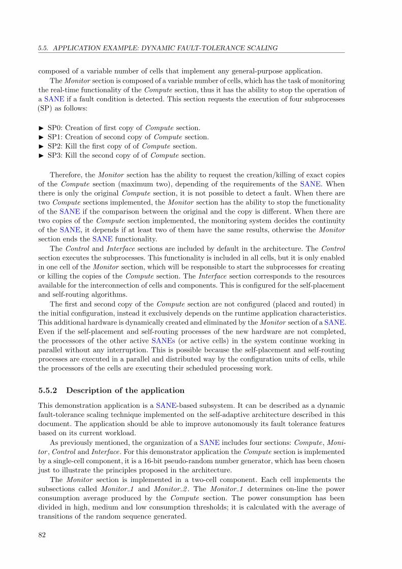
5.5. APPLICATION EXAMPLE: DYNAMIC FAULT-TOLERANCE SCALING
composed of a variable number of cells that implement any general-purpose application.
The Monitor section is composed of a variable number of cells, which has the task of monitoringthe real-time functionality of the Compute section, thus it has the ability to stop the operation ofa SANE if a fault condition is detected. This section requests the execution of four subprocesses(SP) as follows:
I SP0: Creation of first copy of Compute section.I SP1: Creation of second copy of Compute section.I SP2: Kill the first copy of of Compute section.I SP3: Kill the second copy of of Compute section.
Therefore, the Monitor section has the ability to request the creation/killing of exact copiesof the Compute section (maximum two), depending of the requirements of the SANE. Whenthere is only the original Compute section, it is not possible to detect a fault. When there aretwo Compute sections implemented, the Monitor section has the ability to stop the functionalityof the SANE if the comparison between the original and the copy is different. When there aretwo copies of the Compute section implemented, the monitoring system decides the continuityof the SANE, it depends if at least two of them have the same results, otherwise the Monitorsection ends the SANE functionality.
The Control and Interface sections are included by default in the architecture. The Controlsection executes the subprocesses. This functionality is included in all cells, but it is only enabledin one cell of the Monitor section, which will be responsible to start the subprocesses for creatingor killing the copies of the Compute section. The Interface section corresponds to the resourcesavailable for the interconnection of cells and components. This is configured for the self-placementand self-routing algorithms.
The first and second copy of the Compute section are not configured (placed and routed) inthe initial configuration, instead it exclusively depends on the runtime application characteristics.This additional hardware is dynamically created and eliminated by the Monitor section of a SANE.Even if the self-placement and self-routing processes of the new hardware are not completed,the processors of the other active SANEs (or active cells) in the system continue working inparallel without any interruption. This is possible because the self-placement and self-routingprocesses are executed in a parallel and distributed way by the configuration units of cells, whilethe processors of the cells are executing their scheduled processing work.
5.5.2 Description of the application
This demonstration application is a SANE-based subsystem. It can be described as a dynamicfault-tolerance scaling technique implemented on the self-adaptive architecture described in thisdocument. The application should be able to improve autonomously its fault tolerance featuresbased on its current workload.
As previously mentioned, the organization of a SANE includes four sections: Compute, Moni-tor , Control and Interface. For this demonstrator application the Compute section is implementedby a single-cell component, it is a 16-bit pseudo-random number generator, which has been chosenjust to illustrate the principles proposed in the architecture.
The Monitor section is implemented in a two-cell component. Each cell implements thesubsections called Monitor 1 and Monitor 2 . The Monitor 1 determines on-line the powerconsumption average produced by the Compute section. The power consumption has beendivided in high, medium and low consumption thresholds; it is calculated with the average oftransitions of the random sequence generated.
82
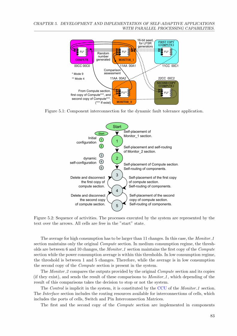
CHAPTER 5. DEVELOPMENT AND IMPLEMENTATION OF SELF-ADAPTIVE APPLICATIONSWITH PARALLEL PROCESSING CAPABILITIES.
FU* FU* FU*
FU** FU*
COMPUTE
11AA--00A1
MONITOR_1
00CC-00C0 11CC--00C1
11AA--00A2 22CC--00C2
MONITOR_2
FIRST COPY(COMPUTE)
SECOND COPY(COMPUTE)
From-Compute-section,-first-copy-of-Compute***,-and-second-copy-of-Compute***.
4***-If-exist)
16-bit-seed,-for-LFSR
generators
Randomnumber
generated
Comparisonassessment*-Mode-9
**-Mode-4
Figure 5.1: Component interconnection for the dynamic fault tolerance application.
1
StartSelf-placementIofMonitor_1Isection.
2
Self-placementIandIself-routingofIMonitor_2Isection.
3
Self-placementIofIComputeIsection.Self-routingIofIcomponents.
4
5
Self-placementIofItheIfirstIcopyofIcomputeIsection.Self-routingIofIcomponents.
Self-placementIofItheIsecondcopyIofIcomputeIsection.Self-routingIofIcomponents.
DeleteIandIdisconnecttheIsecondIcopy
ofIcomputeIsection.
DeleteIandIdisconnecttheIfirstIcopyIof
computeIsection.
Initialconfiguration
dynamicself-configuration
1
2
3
4
5
Start
Figure 5.2: Sequence of activities. The processes executed by the system are represented by thetext over the arrows. All cells are free in the ”start” state.
The average for high consumption has to be larger than 11 changes. In this case, the Monitor 1section maintains only the original Compute section. In medium consumption regime, the thresh-olds are between 6 and 10 changes, the Monitor 1 section maintains the first copy of the Computesection while the power consumption average is within this thresholds. In low consumption regime,the threshold is between 1 and 5 changes. Therefore, while the average is in low consumptionthe second copy of the Compute section is present in the system.
The Monitor 2 compares the outputs provided by the original Compute section and its copies(if they exist), and sends the result of these comparisons to Monitor 1 , which depending of theresult of this comparisons takes the decision to stop or not the system.
The Control is implicit in the system, it is constituted by the CCU of the Monitor 1 section.The Interface section includes the routing resources available for interconnections of cells, whichincludes the ports of cells, Switch and Pin Interconnection Matrices.
The first and the second copy of the Compute section are implemented in components
83

5.6. APPLICATION EXAMPLE: STATIC FAULT-TOLERANCE
Address:(id component
+ id cell)
CellConfiguration
Mode
Description
00CC 00C0 4 Compute section. Generator of a 16-bit pseudo-random number sequence
11AA 00A1 9 Monitor 1 section. Calculates the average consump-tion of the Compute section
11AA 00A2 9 Monitor 2 section. Comparisons of all compute sec-tions.
11CC 00C1 9 First copy of Compute section.
22CC 00C2 9 Second copy of Compute section.
Table 5.10: Description of components for the example application: Dynamic Fault ToleranceScaling.
composed of a single cell. The application for this Compute copies is exactly the same, thepseudo-random number generation. The components developed for this application and theirinterconnections are shown in Figure 5.1 and Table 5.10. The cells in mode 9 have one 16-bitprocessor with capacity for 256 instructions in program memory and 16x16 data memory. Thecell in mode 4 has one 8-bit processor with 32-bytes data memory and 256 instructions capacity.
Figure 5.2 shows the processes executed in the SANE, where it is important to note thedynamic creation and kill processes of copies depending on the changing power consumption ofthe Compute section. Steps “start”, 1 and 2 constitute the initial configuration of basic hardwarerequired for the execution of the application, the Monitor and original Compute section.
Steps 3 to 5 are executed alternately and controlled by the Monitor 1 section, which createsand kills copies of the Compute section depending on its average power consumption.
In the appendix E, Table E.1 presents a relation of the files created and generated by SPDregarding this application. Listings presented in section E.1 show these files.
5.6 Application Example: Static Fault-Tolerance
Lets suppose a 8-bit sequence of data that has to be generated by a processor with a capacity for250 instructions, which has to include a Fault Tolerance System (FTS) to protect the reliabilityof the sequence. The sequence has to be generated at a low speed, much lower than the clockavailable, so it is necessary to implement a delay in the sequence. This could be implemented inthe processor of another cell with a capacity for 50 instructions.
The problem can be solved in many ways, the figure 5.3 shows a specific solution. This SANEincludes three components (AAAA, BBBB and CCCC). The cell identified as AAAA0001 includes theprimary processor, which generates the sequence, and the cell BBBB0002 includes the redundantprocessor that generates the same sequence. These cells are configured in configuration mode 4and in FT mode 5, that allows the FTS of the primary cell making the comparison of 2 cores(Core 0 in primary and redundant cells). The cell CCCC0003 contains a processor that performsthe delay. This will be in mode 0, and its FTS will be disabled (only one processor is used, theother three could be used for future implementations).
When the primary and redundant cells generate one data of the sequence, the OUT0 portof the primary cell is written, producing the Read Enable (RE) flag. This is conducted to thecell CCCC0003, which waits this RE pulse from cell AAAA0001 to start the generation of a delay
84

CHAPTER 5. DEVELOPMENT AND IMPLEMENTATION OF SELF-ADAPTIVE APPLICATIONSWITH PARALLEL PROCESSING CAPABILITIES.
FU
FUFU
AAAAi666hSequenceigenerator,PRIMARY_
BBBBi6662
CCCCi66638ybitisequence
Sequenceigenerator,REDUNDANT_
Modei4liFT_modei5Modei6liFTSiDisabled
DelayModei4:ihiprocessorli
256iinstructionsicapacityiiniprogrami
memoryiandi32ibytesinidataimemoryi Modei6:i4iprocessorsli
64iinstructionsiiniprogramimemoryi
andi8ibytesiinidatamemoryieachione
Figure 5.3: Components configuration for Static Fault Tolerance application example.
(this RE is received by means of the special instruction called BLMOV ”Blocked Move”, whichreads the port, saves the data in a memory location and follows with the next instruction whena RE pulse is produced). The data read is not important for the cell that produces the delay(CCCC0003). This cell executes the delay algorithm, and then writes any data in its OUT0 port,which produces a RE pulse that has to be conducted to the inputs of the primary and redundantcells. When these cells receive the RE pulse they generate the next data of the special sequence,and so on. While the delay is performed, the primary and redundant processors could calculatethe next data of the sequence in a parallel way.
If the primary or redundant processor have a hardware failure, the cells AAAA0001 andBBBB0002 are self-eliminated, the address FFFF0001 will be fixed in both cells, and they will notbe used in subsequent self-placement operations. Its routing resources continue available. Next,the cells AAAA0001 and BBBB0002 start the self-replication process, it involves the self-placementand self-routing of these cells in another location inside the cell array. Once this process ends,the sequence starts the generation again.
In the appendix E, Table E.2 presents a relation of the files created and generated by SPDregarding this application. Listings presented in section E.2 show these files.
5.7 Conclusions
The high-level configuration file for the description of a SANE ASSEMBLY (SANE-ASM) hasbeen defined as the SANE Assembler (SASM) file. This file is composed of a sequence of SASMinstructions that describes the configuration of the SANE-ASM. The syntax and instructionformat for all SASM instructions has been presented. There are 25 instructions that permits theexecution of the following process:
I Create, delete and interconnect components.I Write the Functional Unit (FU) memory of cells, including the Configuration registers.I Restart, disable or enable the processors in system.I Configuration of system in wait state, which permits the execution of runtime self-configuration
processes in system.I Execution of one to four subprocess, which provides the system with dynamic reconfiguration
capabilities.I Configuration of Static Fault Tolerance mechanism, which provides the system with self-healing
capability.I Instruction to denote the end of the SASM configuration file.
85

5.7. CONCLUSIONS
Two application examples have been presented. The first is the Dynamic Fault ScalingTechnique, which permits to check the dynamic reconfiguration of the system by means ofsubprocesses. This application is able to improve autonomously its fault tolerance features basedon its current workload. Therefore, depending on a specific condition in the functional section ofan application, the system dynamically either creates or kills one or two copies of its functionalsection. The fault tolerance subsystem compares the redundant copies of the functional section,if they exist, so as to decide the continuity of the system depending on eventual failures in thecomparison.
The other mechanism of fault tolerance is a dedicated or Static Fault Tolerance mechanism.It provides redundant processing capabilities that are working continuously. In the applicationexample, when a failure in the execution of a binary sequence in the Primary or Redundantprocessors is detected, the processors in Primary cell are stopped and the self-elimination andself-replication processes start for the cells involved in the failure. These cells will be self-discardedfor future self-placement processes.
86

Chapter 6
Publications and Results
When you have the running spirit,you look forward to life.
Cuando se tiene espıritu de atleta,se tiene ilusion por la vida.
Max Popper (1893 – 1976)
Abstract: This chapter presents the publications performed during the elaboration of
this thesis. Additionally, this chapter shows a summary of the files generated for the appli-
cation , which are divided in three sections: hardware, firmware and software. The synthesis
implementation results of the hardware architecture are presented at the final of the chapter.
6.1 Publications
The following is the list of publications organized from latest to oldest.
6.1.1 Neurocomputing Journal
Title: A self-adaptive hardware architecture with fault tolerance capabilities.
Authors: Javier Soto, Juan Manuel Moreno, Joan Cabestany.
Journal: Neurocomputing, Volume 121, 9 December 2013, Pages 25-31. Advances in Arti-ficial Neural Networks and Machine Learning.
Abstract: This paper describes a Fault Tolerance System (FTS) implemented in a newself-adaptive hardware architecture. This architecture is based on an array ofcells that implements in a distributed way self-adaptive capabilities. The cellincludes a configurable multiprocessor, so it can have between one and fourprocessors working in parallel, with a programmable configuration mode thatallows selecting the size of program and data memories. The self-elimination andself-replication capabilities of cell(s) are performed when the FTS detects a failurein any of the processors that include it, so that this cell(s) will be self-discarded forfuture implementations. Other adaptive capabilities of the system are self-routing,self-placement and runtime self-configuration. Additionally, it is described as anexample application and a software tool that has been implemented to facilitatethe development of applications to test the system.
DOI: http://dx.doi.org/10.1016/j.neucom.2012.10.038
ISSN: 0925-2312
87

6.1. PUBLICATIONS
6.1.2 Advances in Computational Intelligence - IWANN 2011
Title Description of a Fault Tolerance System Implemented in a Hardware Ar-chitecture with Self-adaptive Capabilities
Authors Javier Soto, Juan Manuel Moreno, Joan Cabestany.
Book Title Advances in Computational Intelligence
Book Subtitle 11th International Work-Conference on Artificial Neural Networks confer-ence, IWANN 2011, Torremolinos-Malaga, Spain, June 8-10, 2011, Proceed-ings, Part II.
Other Publisher: Springer Berlin Heidelberg, 2011.Series Volume: 6692, pp 557-564.
Abstract: This paper describes a Fault Tolerance System (FTS) implemented in anew self-adaptive hardware architecture. This architecture is based on anarray of cells that implements in a distributed way self-adaptive capabilities.The cell includes a configurable multiprocessor, so it can have between oneand four processors working in parallel, with a programmable configurationmode that allows selecting the size of program and data memories. Theself-elimination and self-replication capabilities of cell(s) are performedwhen the FTS detects a failure in any of the processors that include it, sothat this cell(s) will be self-discarded for future implementations. Otherself-adaptive capabilities of the system are self-routing, self-placement andruntime self-configuration.
DOI http://dx.doi.org/10.1007/978-3-642-21498-1_70
Print ISBN 978-3-642-21497-4
Online ISBN 978-3-642-21498-1
6.1.3 International Conference - Reconfig’09
Title Implementation of a Dynamic Fault-Tolerance Scaling Technique on a Self-adaptive Hardware Architecture
Authors Javier Soto, Juan Manuel Moreno, Jordi Madrenas, Joan Cabestany.
Publication International Conference on Reconfigurable Computing and FPGAs, 2009.ReConFig ’09, Cancun, Quintana Roo, Mexico, December 9-11, 2009. Pages445-450.
Abstract: The purpose of this paper is to describe a dynamic fault tolerance scaling tech-nique that is supported by the self-adaptive features of a hardware architecturedeveloped within the framework of the AETHER project. The architecture iscomposed of an array of cells that support dynamic and distributed self-routingand self-placement of components in the system. The combination of a largearray of cells together with component-level routing ultimately constitutes aSANE (self-adaptive networked entity). The dynamic fault tolerance scalingtechnique proposed in this paper permits a given subsystem to modify au-tonomously its structure in order to achieve fault detection and fault recovery.The decision to modify or not its organization is based on the actual powerconsumption of the system.
DOI http://dx.doi.org/10.1109/ReConFig.2009.45
Print ISBN 978-1-4244-5293-4
E-ISBN 978-0-7695-3917-1
88

CHAPTER 6. PUBLICATIONS AND RESULTS
6.1.4 International Conference - DCIS 2008
Title Design of a Configurable Multiprocessor for a Self-Adaptive Hardware Archi-tecture
Authors Javier Soto, Juan Manuel Moreno, Jordi Madrenas, Joan Cabestany.
Publication XXIII Conference on Design of Circuits and Integrated Systems (DCIS 2008).ISBN: 978-2-84813-124-5.Grenoble, France. November 12-14, 2008.
Abstract: The purpose of this paper is to describe the design of a configurable multipro-cessor used as a functional unit of a cell that is able to perform self-placementand self-routing. An array of such cells ultimately constitutes a SANE (Self-Adaptive Networked Entity). The Functional Unit includes one to four pro-cessors working in parallel, with a programmable configuration mode thatallows selecting the size of program and data memories. Data processing canbe done in modes of 8, 16, 24 and 32 bits. The architecture includes specialinstructions and specific hardware designed to be compatible with a model ofcomputation based on microthreads.
6.1.5 International Conference - JCRA 08
Title Diseno de un Multiprocesador Configurable y de la Interfaz de Comunicacionespara una Arquitectura de Hardware Auto-Adaptable (Design of a ConfigurableMultiprocessor and the Communication Interface for a Self- Adaptive Hard-ware Architecture)
Authors Javier Soto, Juan Manuel Moreno, Jordi Madrenas, Joan Cabestany.
Publication VIII Jornadas de Computacion Reconfigurables y aplicaciones (JCRA 08)(Universidad Rey Juan Carlos – URJC).ISBN: 978-84-612-5635-8.Pages 295-304.Madrid, Spain, September 18-19, 2008.
Abstract: El proposito de este artıculo es describir el diseno de un multiprocesador con-figurable usado como unidad funcional de una celula que es capaz de realizarprocesos de auto-enrutamiento y auto-emplazamiento. La unidad funcionalincluye de uno a cuatro procesadores trabajando en paralelo, cuyo modo deconfiguracion programable permite seleccionar el tamano de las memorias dedatos (8, 16, 24 o 32 bits) y programa. Este procesador incluye hardware einstrucciones especıficas para ser compatible con un modelo de computacionbasado en microthreads. Se describe tambien el diseno de la interfaz de comu-nicaciones necesaria para la ejecucion de los procesos de auto-emplazamientoy auto-enrutamiento.
89

6.2. CODE GENERATED
6.1.6 International Conference - ReCoSoC’08
Title Communication Infrastructure for a Self-Adaptive Hardware Architecture
Authors Javier Soto, Juan Manuel Moreno, Jordi Madrenas, Joan Cabestany.
Publication Proceedings of the Reconfigurable Communication-centric Systems-on-ChipWorkshop (ReCoSoC’08), ISBN: 978-84-691-3603-4, pp. 175-180, Barcelona,Spain, July 9-11, 2008.
Abstract: The purpose of this paper is to describe the design of a communication interfacebetween a cell array and a global configuration unit to support self-placementand self-routing capabilities. The interface is based on the I2C bus specification.The combination of a large array of such cells together with component-levelrouting ultimately constitutes a SANE (Self-Adaptive Networked Entity).
6.2 Code Generated
This section presents a relation of the code generated for the implementation of the self-adaptivearchitecture presented in this document. This code represents only the final prototype imple-mented. The system developed includes different types of technologies divided in three scenarios:hardware, firmware and software, which are detailed in following sections.
6.2.1 Hardware
The hardware section represents the self-adaptive hardware architecture with parallel processingcapabilities presented along this document. This section was developed in two Virtex4 XilinxFPGAs (XC4VLX60), each one includes the same configuration and hardware description writtenin VHDL code. Some differences has been implemented in the design for differentiating the masterand slave chips in prototype. The FPGA pins configuration is different for these chips, thereforetwo projects were built for the implementation of the prototype. Table 6.1 presents a relationof files, code lines and a brief description of each file generated for prototype. Note that thehardware definition of the Control Microprocessor (CµP) is not included in the list, since it wasgenerated with the Xilinx Platform Studio.
It is important to note that these files only represent the final prototype, which is a reducedapproach of the architecture presented in this dissertation. This is due mainly to the physicallimitations in the FPGAs used for the system implementation. It is worth noting the followingconsideration: in prototype the cell (without CCU) and the SM have 1558 and 1912 code linesrespectively. A previous version of the prototype without FU and with two clusters (3x3 cell arrayeach) was implemented for testing of self-routing and self-placement algorithms. For this case thecell (without CCU) and the SM have 2300 and 11900 code lines respectively. The comparisonof the code lines of a cluster with 2x2 cell array (prototype) and the cluster with 3x3 cell arrayis a reference of the hardware complexity for these approaches, and the main reason for theimplementation of the prototype described in section 2.14.
File Name Lines Description
CCU.vhd 1945 Cell Configuration Unit. Implements all self-adaptive algo-rithms for a cell, mainly for self-placement and self-routingprocesses.
cell NE.vhd1 1558 Routing resources for cell North-East.
cell NW.vhd1 1558 Routing resources for cell North-West.
Continued on next page
90

CHAPTER 6. PUBLICATIONS AND RESULTS
File Name Lines Description
cell SE.vhd1 1558 Routing resources for cell South-East.
cell SW.vhd1 1558 Routing resources for cell South-West.
Cluster array.vhd 833 Instantiation of GCU, cells, SM and PIM.
Commands.vhd 207 Library for global definition of special addresses, com-mands for INET and ENET, and other definitions.
dcm1.vhd 107 Clock divider for obtaining 25 MHz clock.
GCU.vhd 1960 Global Configuration Unit. Interface between CµP andCUs inside chips. Controls the self-adaptive processes in-side a chip.
Matrix.vhd2 1912 Switch Matrix. It includes the routing resources of SM andthe SMCU, which implements the self-adaptive processesinside the SM.
Matrix border.vhd 1172 Pin Interconnection Matrix. It includes the routing re-sources of PIM and the PIMCU, which implements theself-adaptive processes inside the PIM.
System chip.vhd 281 Top module. Instantiation of CµP, cluster array and clockdivider (dcm1).
table.vhd 62 Input/output connection tables.
winning column box.vhd 50 Part of the circuit for cell selection process: leftmost up-permost cell.
Mux15x1.vhd 61 Multiplexer 15x1 for 9-bit data bus. FU inputs.
Mux19x1.vhd 66 Multiplexer 19x1 for 9-bit data bus. Connects the SM portwith the FU inputs in cell.
Mux20x1.vhd 67 Multiplexer 20x1 for 9-bit data bus. SM ports
Mux4x1.vhd 47 Multiplexer 4x1 for 9-bit data bus. Chip ports (PIMports).
Mux5x1.vhd 50 Multiplexer 5x1 for 9-bit data bus. Cell local ports.
Mux7x1.vhd 52 Multiplexer 7x1 for 9-bit data bus. PIM ports.
Mux8x1.vhd 52 Multiplexer 8x1 for 9-bit data bus. Cell remote ports.
alu0.vhd 390 ALU for CORE0.
alu1.vhd 391 ALU for CORE1.
alu2.vhd 391 ALU for CORE2.
alu3.vhd 385 ALU for CORE3.
CM.vhd 115 Control Memory. Same for all cores.
DM.vhd 102 General purpose registers. Same for all cores.
DM4.vhd 316 Configuration and status registers mapped in Data Mem-ory: IN0. . . IN3, OUT0. . . OUT3.
DM5.vhd 385 Configuration and status registers mapped in Data Mem-ory: MODE FAMILY, PORTS, SUBPCSR and FTCSR.
FTS.vhd 143 Description of Fault Tolerance System.
FU.vhd 1211 Functional Unit top module. Instantiation and logic forall modules that belongs to the FU.
PC0.vhd 70 Program Counter for CORE0.
PC1.vhd 67 Program Counter for CORE1.
Continued on next page
91

6.3. FIRMWARE
File Name Lines Description
PC2.vhd 70 Program Counter for CORE2.
PC3.vhd 67 Program Counter for CORE3.
PM.vhd 121 Program memory. Same for all cores.
sum com.vhd 45 Full Adder for design of ALUs.
Total 19425 Total number of VHDL code lines for prototype.
1 Cell with routing resources for two sides (1560 lines approximately). For comparative purposes, ageneric cell with routing resources for four sides may have 2300 lines approximately.2 Switch Matrix with routing resources for two sides and four cells (1900 lines approximately). For
comparative purposes, a SM with routing resources for eight sides and nine cells may have 11900lines approximately.
Table 6.1: List of VHDL files for hardware implementation of prototype.
6.3 Firmware
The firmware section of the application is represented by the control program implemented inthe Control Microprocessor (CµP), which was implemented in the same FPGAs used for thehardware prototype. This firmware was implemented using the microprocessor MicroBlaze, whichwas generated by Xilinx Platform Studio (XPS). It is programmed in C language by means ofthe Xilinx Software Development Kit.
Table 6.2 presents a relation of files, code lines and a brief description of the firmwaredeveloped for the system.
File name Code Lines Description
main.c 1898 Main program implemented in CµP.
print.h 69 Functions for writing data in UART. This information is pre-sented in the communication tab of SPD.
uart.h 602 Uart configuration and algorithms for coomunication with SPDby means of XMODEM-based protocol.
commands.h 217 Definitions of commands and generic values.
Total 2786 Total number of code lines implemented for CµP in prototype.
Table 6.2: List of C files for firmware section of prototype (Control Microprocessor).
6.4 Software
The software section of the system represents the SANE Project Developer (SPD), which isa software tool developed for the creation and edition of projects that can be downloaded toprototype (See appendix D for details). This software was developed in C Sharp (C#) using theMicrosoft Visual C# 2008.
Table 6.3 presents the files, code lines and a brief description of the classes created for theimplementation of the SPD. Note that the list only presents the code created for the application;it is not included the code generated by the developed tool, i.e., it is not included the code thatcontains the configuration of the forms, which is normally created in the files FormX.Designer.cs.
92

CHAPTER 6. PUBLICATIONS AND RESULTS
File Name Lines Description
AppData/ApplicationData.cs 586 Object for serialization of application data.
AppData/FormAppData.cs 736 Form events management for edition of applicationdata.
AppData/FormSaneApps.cs 68 Form events management for configuration of defaultlocation of projects.
AppData/SerializableColor.cs 59 Color object with XML serialization.
AppData/SerializableFont.cs 77 Font object with XML serialization.
Compiler/AsmCodeLine.cs 138 Object used for discrimination of instructions, argu-ments and others when a ASM file is compiled.
Compiler/AsmInstructions.cs 84 Object used for definition of ASM instructions.
Compiler/Compile.cs 1493 Object used for compiling ASM files. Generation ofHEX files.
Compiler/Output.cs 69 Object used for generation of output results for com-piling and building processes.
Compiler/Build.cs 1717 Object used for building the project. Generation ofSHEX and SXM files.
Compiler/SasmCodeLine.cs 162 Object used for discrimination of instructions, argu-ments and others when a SASM files is built.
Compiler/SasmInstructions.cs 74 Object used for definition of SASM instructions.
Figure/Figure.cs 1086 Object for generation of a Figure of prototype.
Form/Form1.cs 1213 Management of events for main Form.
Form/Form2.Tree.cs 435 Partial class Form1. Management of events left tree.
Form/Form3.ProjectTab.cs 1850 Partial class Form1. Management of events forProject Tab.
Form/MenuCommunication.cs 156 Partial class Form1. Management of events for menucommunications.
Form/MenuFile.cs 1488 Partial class Form1. Managements of events for Filemenu.
Form/MenuProject.cs 394 Partial class Form1. Management of events forProject menu.
Form/MenuTools.cs 129 Partial class Form1. Management of events for Toolsmenu.
Form/Tab.cs 93 Object for management of Tab pages.
Other/FormAbout.cs 47 Management of About form for credits in SPD.
Project/Cell.cs 165 Object with the parameters of a cell.
Project/CellsArray.cs 1895 Object for management of the cell array.
Project/Project.cs 985 Object for management of the project.
Comm.cs 1372 Partial class Form1. Management of communica-tions ports and threads.
Common.cs 231 Definition of constant values and static methodscommon for the application.
FindAndReplaceForm.cs 475 Management of events and methods for find andreplace action in text editor.
Continued on next page
93

6.5. SYNTHESIS PROCESS FOR PROTOTYPE
File Name Lines Description
FormNewFileTemplate.cs 530 Management of events and methods for creation ofa new file with template wizard.
FormNewProject.cs 140 Management of events and methods for creation ofnew projects.
FormRenameCell.cs 48 Management of events for edition of cells.
FormSelFileProgFPGA.cs 137 Management of events for selection of file whenWrite process is executed.
Globals.cs 27 Static class with global values for text editormanagement.
Program.cs 29 Main program. Start the execution of SPD, call formain Form - Form1.cs.
SerialPortFixer 207 Solve compatibility problems for communicationports when used alternately with hyperterminal andothers.
Total 18395 Total number of C# code lines for SANE ProjectDeveloper (SPD). This number does not includesthe code generated automatically for configurationof Forms.
Note: Automatic files created for configuration of Forms are not included in this table.
Table 6.3: List of C# files developed for implementation of SANE Project Developer.
6.5 Synthesis Process for Prototype
The results of the synthesis process that shows the usage rate for elements of the architectureare detailed in Table 6.4 (hardware section). The Xilinx Synthesis Technology (XST) was usedfor the system implementation in the device selected. This table shows the usage rate for theFU, a cell, a cluster and a complete chip, this permits to have an idea of the system granularity.The program memory of the FU and the connection table have been implemented by means ofthe RAM blocks available in the FPGA used. After generation of bitstream the total utilizationrate was 80%.
6.6 Conclusions
The publications developed during the elaboration of this thesis project have been presented.They encompass one article in the Journal Neurocomputing and five international conferences,two of which are referenced in electronic publications in Springer Berlin Heidelberg and IEEEXplore Digital Library.
The code generated for the final prototype includes approximately 40.000 code lines dis-tributed in hardware, firmware and software, this code has been developed respectively in thefollowing languages: VHDL, C and C#.
The results of the synthesis processes are presented for the main components of the hardwarearchitecture, this gives an idea of the granularity of the hardware prototype implemented.
94

CHAPTER 6. PUBLICATIONS AND RESULTS
Part (Description) SlicesSlice Flip
Flops4 inputLUTs
RAMB16
FPGA: chip resources, for comparison26624100%
53248100%
53248100%
160100%
Functional Unit: Four-core configurablemulticomputer
19277%
4021%
37156%
42%
cell: the routing resources of two sides wereeliminated
353713%
9921%
677112%
63%
cluster: 2x2 cell array + switch matrix15920
59%4086
7%30315
56%2415%
chip: cluster + GCU + µP of control + pininterconnection matrix
1956073%
963818%
3641868%
5635%
Note: the total utilization rate was 80% after generation of bitstream.
Table 6.4: Results of the synthesis process for the proposed prototype.
95


Chapter 7
Conclusions and Future Work
Somewhere, something incredible is waitingto be known.
En algun sitio algo increıble espera ser descubierto.
Carl Sagan (1934 – 1996)
Abstract: This chapter presents general conclusions related with the architecture devel-
oped. Additionally, some research lines are suggested as future work in this research area.
7.1 Conclusions
A novel self-adaptive hardware architecture with parallel processing capability has been developed.Basically, this is an unconventional MIMD hardware architecture with self-adaptive capabilitiesincluding self-placement and self-routing, which due to its intrinsic design, enable the developmentof systems with runtime self-configuration, self-repair and/or fault tolerance capabilities.
The self-adaptive capabilities of the architecture are executed autonomously and in a dis-tributed way by cells. One of the main features of this architecture is its high degree of parallelism.The major drawback is the configuration of complex applications, where many processors haveto be programmed and synchronized in order to accomplish a specific task. A new high-levelprogramming paradigm has to be implemented, with the purpose of obtaining the maximumperformance of the architecture.
The architecture presented includes a dedicated or static Fault Tolerance mechanism. Itprovides redundant processing capabilities that are working continuously. When a failure in theexecution of a program is detected, the processors of the cell are stopped and the self-eliminationand self-replication processes starts for the cell (or cells) involved in the failure. This cell(s) willbe self-discarded for future self-placement processes.
The runtime self-configuration capability of the system is possible with the execution ofsubprocesses, which can be started by any cell in the system. This dynamic reconfigurationcapability permits the implementation of a Dynamic Fault Tolerance Scaling Technique, whichpermits a given subsystem to modify autonomously its structure in order to achieve fault detectionand fault recovery. It has the ability to create and eliminate the redundant copies of the functionalsection of a specific application.
A software tool and a hardware prototype that checks the functionality of the system have beendeveloped. The SANE Project Developer (SPD) is an Integrated Development Environment thatpermits in a friendly way the management of projects that will be implemented in the hardware
97

7.1. CONCLUSIONS
prototype. The applications developed provides parallel processing capabilities, and may includeFault Tolerance mechanisms and runtime self-configuration.
7.1.1 About System Architecture
The proposed architecture consists of four conceptual layers:
I First Layer - Cells: the cells implement the self-adaptive capabilities and provide thecomputing capacity of the system.
I Second Layer - Components: the components are composed of interconnected cells.
I Third Layer - SANE: The Self-Adaptive Networked Entity (SANE) layer consists of agroup of interconnected components. The SANE is the basic self-adaptive computing system;it has the ability of monitoring its local environment and its internal computation process.
I Fourth Layer - SANE-ASM: The top layer, the SANE ASSEMBLY (SANE-ASM) iscomposed of a group of interconnected SANEs.
The proposed architecture is composed of one or more chips and an External Controller(EC), which are interconnected by means of an External Network (ENET). Each chip includes atwo-layers implementation with interconnected cells in the first level and interconnected SMs inthe second level. The SANE and SANE-ASM are just conceptual and are implemented in thesame layer of components. The chip includes a cluster array, a Global Configuration Unit (GCU)and Pin Interconnection Matrices (PIMs). The main features of these components are describedbellow:
I Cluster: The cluster is composed of a 3x3 cell array and a Switch Matrix (SM).
• Cell: The cell is the basic element of the proposed self-adaptive architecture. The cellconsists of the Functional Unit (FU), the Cell Configuration Unit (CCU) and additionalhardware that allows the interconnection between FU ports of two cells.
* Functional Unit: The FU is in charge of executing the processes scheduled to the cell,i.e, it includes the processing capabilities of the cell. The FU includes four cores. Eachcore contains the digital elements that are used for the construction of a processor. Theprocessor is constituted by the elements of one or more cores. Therefore the FU can havebetween one to four processors working in parallel. There are twelve configuration modes,where the expansion of Data and Program Memory describes the specific configurationmode. Therefore, the data processing of FU could be configured for 8, 16, 24 or 32 bitsand the Program Memories can be joined or not depending on the configuration mode,allowing Program Memory sizes of 64, 128, 192 or 256 instructions. The instruction set ofprocessors is composed of 44 instructions, which includes arithmetic, logic, shift, branch,conditional branch and special instruction for the execution of microthreads.
* Cell Configuration Unit: the CCUs are responsible for the execution of the requiredalgorithms for the implementation of the system self-adaptive capabilities, mainly theself-placement and self-routing algorithms.
• Switch Matrix: The SMs permit to connect cells from two different components. The SMis connected to its eight adjacent neighbors; it is also connected to the nine cells belonging tothe cluster. The Switch Matrix Configuration Unit (SMCU) participates in the componentself-routing process. In this process, the FU output port of a cell in a given component isconnected to the FU input port of a cell in a different component.
98

CHAPTER 7. CONCLUSIONS AND FUTURE WORK
I Global Configuration Unit: The GCU is in charge of controlling the self-adaptive processesinside the chip. The GCU is interconnected with the EC through the ENET and with theinternal components of the chip through the INET. The GCU is the interface between the ECand CUs inside the chip. The GCU receives and translates information related to self-adaptiveprocesses or configuration data.
I Pin Interconnection Matrix: The PIMs are used exclusively for the port interconnectionbetween cells of two components in different chips. The PIM is connected to its three adjacentclusters. The Pin Interconnection Matrix Configuration Unit (PIMCU) participates in thecomponent self-routing process, to allow for the interconnection of the FU port of a cell witha pin of the chip. Previously to this configuration, the GCU undertook a negotiation processwith other chips, with the aim of assigning a pin of the chip to connect these components.
The INET, ENET and Configuration Units (CUs) participate actively in all self-adaptiveprocesses implemented in the architecture.
7.1.2 About the Self-Adaptive Processes
All self-adaptive processes described in this dissertation have been implemented and tested inthe hardware prototype. The algorithms presented are te base for the implementation of thehigh-level instructions in the system. These algorithms are executed by the Configuration Unitsand are presented bellow:
I The self-placement algorithm: it is responsible for finding out the most suitable positionto insert the new cell of a component. For the placement of the first cell of a component, aparticular procedure is used, different from other cells. In this case, a good candidate positionis defined as one where a free cell has low routing congestion and the largest number of freeneighboring cells. After the insertion of the component first cell, the next cells to be insertedare placed as close as possible to the cell with the largest number of connections with the newcell.
I The self-routing algorithm: it permits to connect the Functional Unit ports of two cells.This process can be executed at cell or component level. The self-routing process at celllevel is executed since the insertion of the second cell of a component, each time that theself-placement process ends. The algorithm allows interconnecting the ports of the functionalunit of two cells, in the same component, through the local and remote cell ports. Afterthe insertion of all components, the self-routing process at component level can be executed.This algorithm implements the interconnection of two cells belonging to different componentsthrough Switch and Pin Interconnection Matrices.
I The self-derouting algorithm: it permits to release all routing resources used to in-terconnect cells or components. This process can be executed for a single cell or a entirecomponent. For this purpose, the Release Process is implemented. This process releases therouting resources (multiplexers) used for an interconnection between cells.
I Self-configuration: The elimination of a single cell and the deletion of a entire componentare processes used by the runtime self-configuration capabilities included in the system: (1) theStatic Fault Tolerance mechanism is able to execute the self-replication and self-elimination ofcells, and, (2) the dynamic reconfiguration by means of subprocess can execute the creation,connection and deletion of components, among others.
99

7.2. FUTURE WORK
7.1.3 About Integrated Development System
The proposed hardware architecture has been implemented and tested in a hardware prototypedeveloped in VHDL for two chips (boards with Virtex 4 Xilinx FPGAs). Additionally, an Inte-grated Development Environment has been developed. This software tool called SANE ProjectDeveloper (SPD) permits the implementation of general purpose applications that include allcapabilities presented along the document.
The hardware and software tools constitute the Integrated Development System, whichpermits to create projects that implement the self-adaptive and parallel processing capabilitiespresented in this dissertation. The following are some features supported by the system:
I The high-level configuration file for the description of a SANE ASSEMBLY (SANE-ASM)has been defined as the SANE Assembler (SASM) file.
I The SASM file is composed of a sequence of SASM instructions that describe the configurationof the SANE-ASM. The syntax and instruction format for all SASM instructions have beenpresented. There are 25 instructions that permit the execution of the following processes:
• Create, delete and interconnect components.• Write the Functional Unit (FU) memory of cells, including the Configuration registers.• Restart, disable or enable the processors in system.• Configuration of system in a special state called wait, which permits the execution of runtime
self-configuration processes in system.• Execution of one to four subprocesses, which provides the system with dynamic reconfigu-
ration capabilities.• Configuration of Static Fault Tolerance mechanism, which provides the system with self-
healing capability.• Instruction to denote the end of the SASM configuration file.
Two application examples have been presented. These applications has been selected becausethey include all self-adaptive, parallel processing and fault tolerance capabilities developed forthe architecture.
I The first is the Dynamic Fault Tolerance Scaling Technique, which permits to check thedynamic reconfiguration of the system by means of subprocesses. This application is able toimprove autonomously its fault tolerance features based on its current workload. Therefore,depending on a specific condition in the functional section of an application, the systemdynamically either creates or kills one or two copies of its functional section. The faulttolerance subsystem compares the redundant copies of the functional section, if they exist, soas to decide the continuity of the system depending on eventual failures in the comparison.
I The other mechanism of fault tolerance is a dedicated or Static Fault Tolerance mechanism. Itprovides redundant processing capabilities that are working continuously. In the applicationexample, when a failure in the execution of a binary sequence in the Primary or Redundantprocessors is detected, the processors in Primary cell are stopped and the self-eliminationand self-replication processes start for the cells involved in the failure. These cells will beself-discarded for future self-placement processes.
7.2 Future Work
Some research topics that can be studied in the future are discussed as follows:
100

CHAPTER 7. CONCLUSIONS AND FUTURE WORK
I Integration or development of a new high-level programming paradigm that permits thedevelopment of complex application with the features of the architecture presented in thisdissertation. The purpose of this is obtaining the maximum performance of the architecture.References [29] [30] [31] [32] present relevant information about this point.
I A software model for self-adaptive architectures has been developed for the AETHER project [30].The SANE Virtual Processor (SVP) is a thread-based model of concurrent program compo-sition as a basis for designing and programming many-core chips. The model is based inmicrothreads, which are small code fragments that can be run concurrently to gain increasedperformance in the proposed self-adaptive hardware architecture. As mentioned previously, theintegration of a new high-level software model like this and the proposed hardware architectureconstitutes an important advance for the development of complex applications.
I Depending of the programming paradigm exposed in the previous items, it must be consideredthe implementation of a C compiler, which involves the creation of a back-end for the FunctionalUnits processors in the cell.
I Implementation of a larger array of elements in both scenarios: chips and cell. If a prototypewith more cells is implemented inside a chip, the architecture and self-adaptive algorithmshould not be modified unless mew capabilities will be implemented. If more than two chipsare included in a prototype, some negotiation processes must be redesigned to achieve thenegotiation between chips, which is mainly used for interconnection of components in differentchips.
I If a larger array of clusters inside a chip is achieved, the interface between chips currentlyimplemented with Pin Interconnections Matrices must be redefined. Similarly, an externalinterface must be defined for chips, with the purpose of implementing general purpose ap-plications that control external devices, or in general terms that permit to communicate thesystem with another digital device.
101


Appendix A
Instructions Set for Functional UnitProcessors
The integrity of men is to be measured by theirconduct, not by their professions.
La integridad del hombre se mide por suconducta, no por sus profesiones.
Decimo Junio Juvenal (60 – 128)
Abstract: This section shows all relevant information related with the instruction set for
Functional Unit processor(s). The instructions are summarized in a table and described in
alphabetical order for easy reference.
A.1 Instructions Format
Each instruction is a 25-bit word divided into an opcode and operands. The opcode representsthe unique identifier of the instruction. The remaining bits of the instructions represents theoperands that specifies the operation of the instruction. The instruction formats are presentedin Figure A.1, while their fields are summarized in Table A.1.
The FU instruction formats are divided in the next categories:
I Operations with literal and registers: W and F represent data memory registers and’k’ represents a 8-bit literal or constant value. For processors with data length greater than8 bits, the other bits of ’k’ must be assumed as 0’s. The destination selector ’d’ is useful toassign a byte in a specific position of the entire word without modifying the other bytes, e.g.,a 32-bit constant value could be assigned using four instructions MOVLF.
I Operations with three registers: W and Y represent data source resisters, while F repre-sents the operation destination register. It is important to note that there is not restrictionin the use of source and destination registers i.e. the source and destination registers couldbe the same, any combination is possible.
I Operations with two registers: W and F represent source and destination register respec-tively. These registers could be the same, therefore the source register could be modified inthe same operation. INP represents a register located between address 0x20 and 0x23, wichrepresents different combination of input ports which depends on configuration mode andprocessor used.
103

A.2. INSTRUCTIONS SET
Operations with Literal and Registers
Operations with three Registers
Operations with two Register
OPCODE k W F
OPCODE k x x x x Fd d
0561112192024
56712192024 0
OPCODE Y0561112171824
056111824
x x x x x x1217
1 0 0 0 P P
W F
W FOPCODE
Fx x x x x xOPCODE
Bit-oriented operations056111824
x b b b b b1217
0561112192024
F FOPCODE
x b b b b bWkOPCODE
Conditional/Unconditional branch operations
x x x x x x x x x x x x 01112192024
0561112192024
0561112192024
kOPCODE
YWkOPCODE
FWkOPCODE
Miscelaneous operations0561824
x x x x x x x x x x x x17
01824
x x x x x x x x x x x x x x x x x x17
FOPCODE
OPCODE056111824 1217
Figure A.1: Instructions format.
I Bit-oriented operations: F represents the register that will be affected in a set or clearbit operation, i.e., F is the source and destination register at the same time. W representsthe source register used for a conditional branch to address k that depends on a bit value. ’b’represents a bit field designator which selects the bit affected by the operation. Some of theseoperations include conditional operations.
I Operations with conditional and unconditional branches: W and Y represent datasource resisters, these registers will not be affected during comparison operations. F representsthe operation destination register. ’k’ represents the absolute destination address for thisoperations.
I Miscellaneous operations: In these operations F represents the destination register.
A.2 Instructions Set
The nomenclature shown in Table A.2 is used in the instruction descriptions throughout thissection. Table A.3 shows the assembler instructions for the FU processors. Thereafter, all in-structions are organized alphabetically and detailed individually. Each instruction is executedin one single clock. The oscillator frequency for processors in the prototype is 25 MHz, thereforeeach instruction is executed in 40 ns.
104
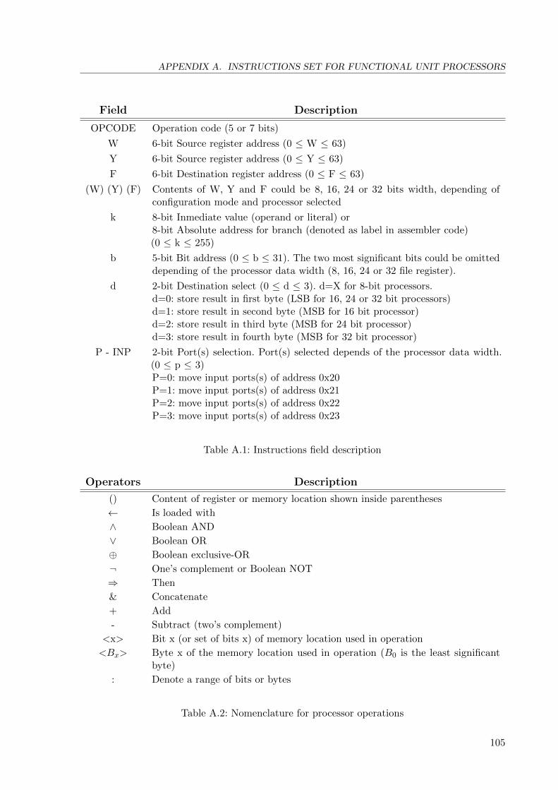
APPENDIX A. INSTRUCTIONS SET FOR FUNCTIONAL UNIT PROCESSORS
Field Description
OPCODE Operation code (5 or 7 bits)
W 6-bit Source register address (0 ≤ W ≤ 63)
Y 6-bit Source register address (0 ≤ Y ≤ 63)
F 6-bit Destination register address (0 ≤ F ≤ 63)
(W) (Y) (F) Contents of W, Y and F could be 8, 16, 24 or 32 bits width, depending ofconfiguration mode and processor selected
k 8-bit Inmediate value (operand or literal) or8-bit Absolute address for branch (denoted as label in assembler code)(0 ≤ k ≤ 255)
b 5-bit Bit address (0 ≤ b ≤ 31). The two most significant bits could be omitteddepending of the processor data width (8, 16, 24 or 32 file register).
d 2-bit Destination select (0 ≤ d ≤ 3). d=X for 8-bit processors.d=0: store result in first byte (LSB for 16, 24 or 32 bit processors)d=1: store result in second byte (MSB for 16 bit processor)d=2: store result in third byte (MSB for 24 bit processor)d=3: store result in fourth byte (MSB for 32 bit processor)
P - INP 2-bit Port(s) selection. Port(s) selected depends of the processor data width.(0 ≤ p ≤ 3)P=0: move input ports(s) of address 0x20P=1: move input ports(s) of address 0x21P=2: move input ports(s) of address 0x22P=3: move input ports(s) of address 0x23
Table A.1: Instructions field description
Operators Description
() Content of register or memory location shown inside parentheses
← Is loaded with
∧ Boolean AND
∨ Boolean OR
⊕ Boolean exclusive-OR
¬ One’s complement or Boolean NOT
⇒ Then
& Concatenate
+ Add
- Subtract (two’s complement)
<x> Bit x (or set of bits x) of memory location used in operation
<Bx> Byte x of the memory location used in operation (B0 is the least significantbyte)
: Denote a range of bits or bytes
Table A.2: Nomenclature for processor operations
105

A.2. INSTRUCTIONS SET
Mnemonic,Operands
Description 25-bit Instruction CodeCCR
Afected
LITERAL AND REGISTERS ORIENTED OPERATIONS
ADDLW W,k,F Add Literal and W 00000 kkkkkkkk wwwwww ffffff C,Z
SUBLW W,k,F Subtract Literal and W 00001 kkkkkkkk wwwwww ffffff C,Z
ANDLW W,k,F AND Literal with W 00010 kkkkkkkk wwwwww ffffff Z
IORLW W,k,F Inclusive OR Literal with W 00011 kkkkkkkk wwwwww ffffff Z
XORLW W,k,F Exclusive OR Literal with W 00100 kkkkkkkk wwwwww ffffff Z
MOVLF k,F,d Move Literal to F 00101 kkkkkkkk xxxxdd ffffff -
THREE REGISTERS ORIENTED OPERATIONS
ADDWY W,Y,F Add W and Y 00110 00yyyyyy wwwwww ffffff C,Z
SUBWY W,Y,F Subtract W and Y 00110 01yyyyyy wwwwww ffffff C,Z
ANDWY W,Y,F AND W with Y 00110 10yyyyyy wwwwww ffffff Z
IORWY W,Y,F Inclusive OR W with Y 00110 11yyyyyy wwwwww ffffff Z
XORWY W,Y,F Exclusive OR W with Y 00111 00yyyyyy wwwwww ffffff Z
TWO REGISTER ORIENTED OPERATIONS
MOVW W,F Move W to F 00111 01xxxxxx wwwwww ffffff Z
BLMOV INP,F Blocked Move of INP to F 00111 10xxxxxx 1000pp ffffff Z
COMW W,F One’s complement of W 00111 11xxxxxx wwwwww ffffff Z
NEGW W,F Two’s complement of W 01000 00xxxxxx wwwwww ffffff C,Z
INCW W,F Increment W 01000 01xxxxxx wwwwww ffffff Z
DECW W,F Decrement W 01000 10xxxxxx wwwwww ffffff Z
SWAPW W,F Swap halves in W 01000 11xxxxxx wwwwww ffffff -
RLW W,F Rotate left through Carry 01001 00xxxxxx wwwwww ffffff C,Z
RRW W,F Rotate right through Carry 01001 01xxxxxx wwwwww ffffff C,Z
LSL W,F Logical shift left (Same as ASL) 01001 10xxxxxx wwwwww ffffff C,Z
LSR W,F Logical shift right 01001 11xxxxxx wwwwww ffffff C,Z
ASL W,F Arithmetic shift left (Same as LSL) 01001 10xxxxxx wwwwww ffffff C,Z
ASR W,F Arithmetic shift right 01010 00xxxxxx wwwwww ffffff C,Z
MISCELANEOUS OPERATIONS
CLRF F Clear F 01010 01xxxxxx xxxxxx ffffff Z
CLC Clear carry bit 01010 10xxxxxx xxxxxx xxxxxx C
SEC Set carry bit 01010 11xxxxxx xxxxxx xxxxxx C
END End of execution 01011 00xxxxxx xxxxxx xxxxxx TA
NOP No operation 01011 01xxxxxx xxxxxx xxxxxx -
BIT-ORIENTED (CONDITIONAL) OPERATIONS
BCLR F,b Clear bit b in F 01011 10-bbbbb ffffff ffffff -
BSET F,b Set bit b in F 01011 11-bbbbb ffffff ffffff -
BRCLR W,b,k Branch if bit b in W clear 01100 kkkkkkkk wwwwww -bbbbb -
BRSET W,b,k Branch if bit b in W set 01101 kkkkkkkk wwwwww -bbbbb -
CONDITIONAL AND UNCONDITIONAL BRANCH OPERATIONS
GOTO k Go to address 01110 kkkkkkkk xxxxxx xxxxxx -
BZ k Branch if Z bit set 01111 kkkkkkkk xxxxxx xxxxxx -
BNZ k Branch if Z bit clear 10000 kkkkkkkk xxxxxx xxxxxx -
BC k Branch if Carry bit set 10001 kkkkkkkk xxxxxx xxxxxx -
BNC k Branch if Carry bit clear 10010 kkkkkkkk xxxxxx xxxxxx -
CBEQ W,Y,k Compare and Branch if Equal 10011 kkkkkkkk wwwwww yyyyyy -
CBGE W,Y,k Compare and Branch if greater than 10100 kkkkkkkk wwwwww yyyyyy -
or equal to
CBGT W,Y,k Compare and Branch if greater than 10101 kkkkkkkk wwwwww yyyyyy -
CBNE W,Y,k Compare and Branch if not Equal 10110 kkkkkkkk wwwwww yyyyyy -
DBNZ W,F,k Decrement and Branch if Not Zero 10111 kkkkkkkk wwwwww ffffff -
IBNZ W,F,k Increment and Branch if Not Zero 11000 kkkkkkkk wwwwww ffffff -
Table A.3: Instructions set summary106

APPENDIX A. INSTRUCTIONS SET FOR FUNCTIONAL UNIT PROCESSORS
ADDLW Add Literal and register W
Syntax: ADDLW W,k,F
Operation: (F) ← (W) + k
Description: The contents of the register W are added to the eight-bit literal ’k’ and theresult is placed in the register F. For modes of 16, 24 and 32 bits, the mostsignificant bits of ’k’ must be assumed as 0’s.
ADDWY Add registers W and Y
Syntax: ADDWY W,Y,F
Operation: (F) ← (W) + (Y)
Description: The contents of the register W are added to the contents of register Y and theresult is placed in the register F.
ANDLW AND Literal with register W
Syntax: ANDLW W,k,F
Operation: (F) ← (W) ∧ k
Description: Performs the logical AND between the contents of register W and literal ’k’and places the result in register F. For modes of 16, 24 and 32 bits, the mostsignificant bits of ’k’ must be assumed as 0’s.
ANDWY AND register W with register Y
Syntax: ANDWY W,Y,F
Operation: (F) ← (W) ∧ (Y)
Description: Performs the logical AND between the contents of register W and register Yand places the result in register F.
ASL Arithmetic shift left
Syntax: ASL W,F
Operation: 8-bit: C ← (W)<7>, (F) ← (W)<6:0> & 016-bit: C ← (W)<15>, (F) ← (W)<14:0> & 024-bit: C ← (W)<23>, (F) ← (W)<22:0> & 032-bit: C ← (W)<31>, (F) ← (W)<30:0> & 0
Description: The contents of register W are shifted one bit to the left, bit 0 is loaded with a0, the result in placed in register F. The C bit in the CCR is loaded from themost significant bit of W. This is mathematically equivalent to multiplicationby two.
ASR Arithmetic shift right
Syntax: ASR W,F
Operation: 8-bit: (F) ← (W)<7> & (W)<7:1>, C ← (W)<0>16-bit: (F) ← (W)<15> & (W)<15:1>, C ← (W)<0>24-bit: (F) ← (W)<23> & (W)<23:1>, C ← (W)<0>32-bit: (F) ← (W)<31> & (W)<31:1>, C ← (W)<0>
Description: The contents of register W are shifted one bit to the right, most significant bitheld constant, the result in placed in register F. The C bit in the CCR is loadedfrom bit 0 of W. This operation effectively divides a signed value by 2 withoutchanging its sign. The carry bit can be used to round the result.
107

A.2. INSTRUCTIONS SET
BC Branch if Carry bit set
Syntax: BC k
Operation: if (C) = 1 ⇒ PC ← k
Description: Tests the state of the C bit in the CCR and causes a branch if C is set. BC canbe used after any instructions that affect the C bit in register CCR.
BCLR Clear bit b in F
Syntax: BCLR F,b
Operation: (F)<b> ← 0
Description: Bit ’b’ in register F is cleared. Bits b<2:0> are used for 8-bit processors. Bitsb<3:0> are used for 16-bit processors. All bits of b are used for 24-bit and32-bit processors. If the value used in ’b’ is out of appropriate range of valuesfor 8, 16 and 24 bit processors, the result might not be as expected.
BLMOV Blocked Move of INP to F
Syntax: BLMOV INP,F
Operation: if (RE) = 1 ⇒ (F) ← (0x20 + INP), (PC)++else ⇒ (PC) ← (PC)
Description: Moves INP to register F when Read Enable pulse(s) is(are) active. INP=[0,1,2,3]represents any address between 0x20 and 0x23 respectively, each address cancontain one or more input ports, depending on the data processing width. REis set during a clock pulse when a processor writes any output port(s) (address0x24 to 0x27). Examples:8-bit: for INP=3, (F)←(0x23) when RE pulse at IN3; for INP ∈ [0,1,2,3]16-bit: for INP=1, (F)←(0x21) when RE pulses at IN2 IN3; for INP ∈ [0,1]24-bit: for INP=0, (F)←(0x20) when RE pulses at IN0 IN1 IN2; INP ∈ [0]32-bit: for INP=0, (F)←(0x20) when RE pulses at IN0 IN1 IN2 IN3; INP∈[0]
BNC Branch if Carry bit clear
Syntax: BNC k
Operation: if (C) = 0 ⇒ PC ← k
Description: Tests the state of the C bit in the CCR and causes a branch if C is clear. BCcan be used after any instructions that affects the C bit in register CCR.
BNZ Branch if Z bit clear
Syntax: BNZ k
Operation: if (Z) = 0 ⇒ PC ← k
Description: Tests the state of the Z bit in the CCR and causes a branch if Z is clear. BZcan be used after any instructions that affects the Z bit in register CCR.
BRCLR Branch if bit b in W clear
Syntax: BRCLR W,b,k
Operation: if (W)<b> = 0 ⇒ PC ← k
Description: Test bit n of register W and branches if the bit is clear. Bits b<2:0> are usedfor 8-bit processors. Bits b<3:0> are used for 16-bit processors. All bits ofb are used for 24-bit and 32-bit processors. If the value used in ’b’ is out ofappropriate range of values for 8, 16 and 24 bit processors, the result might notbe as expected.
108

APPENDIX A. INSTRUCTIONS SET FOR FUNCTIONAL UNIT PROCESSORS
BRSET Branch if bit b in W set
Syntax: BRSET W,b,k
Operation: if (W)<b> = 1 ⇒ PC ← k
Description: Test bit n of register W and branches if the bit is set. Bits b<2:0> are usedfor 8-bit processors. Bits b<3:0> are used for 16-bit processors. All bits ofb are used for 24-bit and 32-bit processors. If the value used in ’b’ is out ofappropriate range of values for 8, 16 and 24 bit processors, the result might notbe as expected.
BSET Set bit b in F
Syntax: BSET F,b
Operation: (F)<b> ← 1
Description: Bit ’b’ in register F is set. Bits b<2:0> are used for 8-bit processors. Bitsb<3:0> are used for 16-bit processors. All bits of b are used for 24-bit and32-bit processors. If the value used in ’b’ is out of appropriate range of valuesfor 8, 16 and 24 bit processors, the result might not be as expected.
BZ Branch if Z bit set
Syntax: BZ k
Operation: if (Z) = 1 ⇒ PC ← k
Description: Tests the state of the Z bit in the CCR and causes a branch if Z is set. BZ canbe used after any instructions that affects the Z bit in register CCR.
CBEQ Compare and branch if equal
Syntax: CBEQ W,Y,k
Operation: if (W) = (Y) ⇒ PC ← k
Description: Compares the contents of register W against the contents of register Y andcauses a branch if the contents are equal.
CBGE Compare and branch if greater than or equal to
Syntax: CBGE W,Y,k
Operation: if (W) ≥ (Y) ⇒ PC ← k
Description: The instruction causes a branch if the contents of register W is greater than orequal to the contents of register Y. The instruction assumes unsigned values inthe registers.
CBGT Compare and branch if greater than
Syntax: CBGT W,Y,k
Operation: if (W) > (Y) ⇒ PC ← k
Description: The instruction causes a branch if the contents of register W is greater than thecontents of register Y. The instruction suppose unsigned values in the registers.
CBNE Compare and branch if not equal
Syntax: CBNE W,Y,k
Operation: if (W) 6= (Y) ⇒ PC ← k
Description: Compares the contents of register W against the contents of register Y andcauses a branch if the contents are not equal..
109

A.2. INSTRUCTIONS SET
CLC Clear Carry bit
Syntax: CLC
Operation: C ← 0
Description: Clears the C bit in the CCR. CLC may be used to set up the C bit prior to ashift or rotate instruction that involves the C bit. The C bit can also be usedto pass status information between subroutines.
CLRF Increment W
Syntax: CLRF F
Operation: (F) ← 0
Description: The contents of register F is cleared, the Z bit in CCR is set.
COMW One’s complement of W
Syntax: COMW W,F
Operation: (F) ← ¬(W)
Description: Performs the one’s complement of the contents of register W and places theresult in register F.
DBNZ Decrement and branch if not Zero
Syntax: DBNZ W,F,k
Operation: (F) ← (W) - 1, if (Z) = 0 ⇒ PC ← k
Description: The contents of register W is decremented, the result in placed in register F.The instruction causes a branch if the result is not 0.
DECW Decrement W
Syntax: DECW W,F
Operation: (F) ← (W) - 1
Description: The contents of register W is decremented, the result in placed in register F.
END End of execution
Syntax: END
Operation: PC ← PC, TA ← 0
Description: Ends the execution of instructions by the processor. Clears the TA bit in theCCR.
GOTO Go to address
Syntax: GOTO k
Operation: PC ← k
Description: GOTO is an unconditional branch. The 8-bit immediate value is loaded intoPC bits.
IBNZ Increment and branch if not Zero
Syntax: IBNZ W,F,k
Operation: (F) ← (W) + 1, if (Z) = 0 ⇒ PC ← k
Description: The contents of register W is incremented, the result in placed in register F.The instruction causes a branch if the result is not 0.
110

APPENDIX A. INSTRUCTIONS SET FOR FUNCTIONAL UNIT PROCESSORS
INCW Increment W
Syntax: INCW W,F
Operation: (F) ← (W) + 1
Description: The contents of register W is incremented, the result in placed in register F.
IORLW Inclusive OR Literal with register W
Syntax: IORLW W,k,F
Operation: (F) ← (W) ∨ k
Description: Performs the logical inclusive-OR between the contents of register W and literal’k’ and places the result in register F. For modes of 16, 24 and 32 bits, the mostsignificant bits of ’k’ must be assumed as 0’s.
IORWY Inclusive OR register W with register Y
Syntax: IORWY W,Y,F
Operation: (F) ← (W) ∨ (Y)
Description: Performs the logical inclusive-OR between the contents of register W and registerY and places the result in register F.
LSL Logical shift left
Syntax: LSL W,F
Operation: 8-bit: C ← (W)<7>, (F) ← (W)<6:0> & 016-bit: C ← (W)<15>, (F) ← (W)<14:0> & 024-bit: C ← (W)<23>, (F) ← (W)<22:0> & 032-bit: C ← (W)<31>, (F) ← (W)<30:0> & 0
Description: The contents of register W are shifted one bit to the left, bit 0 is loaded with a0, the result in placed in register F. The C bit in the CCR is loaded from themost significant bit of W.
LSR Logical shift right
Syntax: LSR W,F
Operation: 8-bit: (F) ← 0 & (W)<7:1>, C ← (W)<0>16-bit: (F) ← 0 & (W)<15:1>, C ← (W)<0>24-bit: (F) ← 0 & (W)<23:1>, C ← (W)<0>32-bit: (F) ← 0 & (W)<31:1>, C ← (W)<0>
Description: The contents of register W are shifted one bit to the right, most significant bitis loaded with a 0, the result in placed in register F. The C bit in the CCR isloaded from the bit 0 of W.
MOVLF Move Literal to F
Syntax: MOVLF k,F,d
Operation: (F)<d> ← k
Description: Moves the literal ’k’ to any byte of register F, depending of destination ’d’.8-bit: (F)←k for any value of ’d’.16-bit: for d=1, (F)<B1 >←k, (F)<B0>←(F)<B0>. If d6=[0,1], (F)←(F).24-bit: for d=2, (F)<B2>←k, (F)<B1:B0>←(F)<B1:B0>. If d6=[0,1,2], F←F.32-bit: for d=3, (F)<B3>←k, (F)<B2:B0>←(F)<B2:B0>
111

A.2. INSTRUCTIONS SET
MOVW Move W to F
Syntax: MOVW W,F
Operation: (F) ← (W)
Description: Moves the contents of register W to register F.
NEGW Two’s complement of W
Syntax: NEGW W,F
Operation: (F) ← ¬(W) + 1
Description: Performs the two’s complement of the contents of register W and places theresult in register F.
NOP No operation
Syntax: NOP
Operation: None (PC ← PC + 1)
Description: This is an instruction that does nothing except to consume one CPU clock cyclewhile the program counter is advanced to the next instruction. No register ormemory contents are affected by this instruction.
RLW Rotate Left through Carry
Syntax: RLW W,F
Operation: 8-bit: C ← (W)<7>, (F) ← (W)<6:0> & C16-bit: C ← (W)<15>, (F) ← (W)<14:0> & C24-bit: C ← (W)<23>, (F) ← (W)<22:0> & C32-bit: C ← (W)<31>, (F) ← (W)<30:0> & C
Description: The contents of register W are rotated one bit to the left through the Carry,the result in placed in register F.
RRW Rotate Right through Carry
Syntax: RRW W,F
Operation: 8-bit: (F) ← C & (W)<7:1>, C ← (W)<0>16-bit: (F) ← C & (W)<15:1>, C ← (W)<0>24-bit: (F) ← C & (W)<23:1>, C ← (W)<0>32-bit: (F) ← C & (W)<31:1>, C ← (W)<0>
Description: The contents of register W are rotated one bit to the right through the Carry,the result in placed in register F.
SEC Set Carry bit
Syntax: SEC
Operation: C ← 1
Description: Clears the C bit in the CCR. CLC may be used to set up the C bit prior to ashift or rotate instruction that involves the C bit. The C bit can also be usedto pass status information between subroutines.
SUBLW Subtract Literal from register W
Syntax: SUBLW W,k,F
Operation: (F) ← (W) - k
Description: Subtracts the contents of literal ’k’ from register W and places the result inregister F (2’s complement method). For modes of 16, 24 and 32 bits, the mostsignificant bits of ’k’ must be assumed as 0’s.
112

APPENDIX A. INSTRUCTIONS SET FOR FUNCTIONAL UNIT PROCESSORS
SUBWY Subtracts registers W and Y
Syntax: SUBWY W,Y,F
Operation: (F) ← (W) - (Y)
Description: Subtracts the contents of register Y from register W and places the result inregister F (2’s complement method).
SWAPW Swap halves of W
Syntax: SWAPW W,F
Operation: 8-bit: (F)<7:4> ← (W)<3:0>, (F)<3:0> ← (W)<7:4>16-bit: (F)<15:8> ← (W)<7:0>, (F)<7:0> ← (W)<15:8>24-bit: (F)<23:12> ← (W)<11:0>, (F)<11:0> ← (W)<23:12>32-bit: (F)<31:16> ← (W)<15:0>, (F)<15:0> ← (W)<31:16>
Description: Swaps upper and lower halves of the contents of register W, the result in placedin register F.
XORLW Exclusive OR Literal with register W
Syntax: XORLW W,k,F
Operation: (F) ← (W) ⊕ k
Description: Performs the logical exclusive-OR between the contents of register W and literal’k’ and places the result in register F. For modes of 16, 24 and 32 bits, the mostsignificant bits of ’k’ must be assumed as 0’s.
XORWY Exclusive OR register W with register Y
Syntax: XORWY W,Y,F
Operation: (F) ← (W) ⊕ (Y)
Description: Performs the logical exclusive-OR between the contents of register W andregister Y and places the result in register F.
113


Appendix B
Data Memory Registers ofFunctional Unit Processors
Don’t walk in front of me; I may not follow.Don’t walk behind me; I may not lead.Just walk beside me and be my friend.
No camines delante de mı, puede que no te siga.No camines detras de mı, puede que no te guıe.
Camina junto a mı y se mi amigo.
Albert Camus (1913 – 1960)
Abstract: This section presents a detailed description of Data Memory registers of FU
processors for all configuration modes and data sizes. The registers are shown in order
according to their address and separated by pages for easy reference.
B.1 Abbreviations
Table B.1 shows the abbreviations used for description of bit registers throughout this section.
Abbreviations
r = Readable bit w = Writable bit u = Unimplemented bit, read as 0
-n = Value at POR/R 1 = Bit is set 0 = Bit is cleared x = Bit is unknown
R = Readable byte W = Writable byte U = Unimplemented byte, read as 00h
-N=Value at POR/R 00-FFh = 8-bit value X = Byte is unknown
POR/R = Power-On Reset or manual reset with push-button.
Table B.1: Abbreviations for bits of Data Memory registers
115

B.2. INPUT PORTS REGISTERS
B.2 Input Ports Registers
The input ports registers are between addresses 20h and 23h. Its configuration is showed below.Note that input ports in a specific address depends of the processors data size.
8-bit ProcessorsInput Ports - IN0, IN1, IN2 and IN3 (ADDRESS 20h, 21h, 22h and 23h)
bit 7 bit 0
INX
r-x r-x r-x r-x r-x r-x r-x r-x
bit 7:0 Value in the input port X (read only registers).IN0 when address is 20hIN1 when address is 21hIN2 when address is 22hIN3 when address is 23h
16-bit ProcessorsInput Ports - IN0 IN1, IN2 IN3 (ADDRESS 20h, 21h)
bit 15 bit 8 bit 7 bit 0
INX INY
R-X R-X
bit 15:0 Value in the concatenation of two 8-bits input ports INX INY(read only registers).IN0 IN1 when address is 20hIN2 IN3 when address is 21hRead 0x0000 for address 22h and 23h
24-bit ProcessorsInput Ports - IN0 IN1 IN2 (ADDRESS 20h)
bit 23 bit 16 bit 15 bit 8 bit 7 bit 0
IN0 IN1 IN2
R-X R-X R-X
bit 23:0 Value in the concatenation of three 8-bits input ports IN0 IN1 IN2 (read onlyregisters). Read 0x000000 for address 21h, 22h and 23h
32-bit ProcessorsInput Ports - IN0 IN1 IN2 IN3 (ADDRESS 20h)
bit 31 bit 24 bit 23 bit 16 bit 15 bit 8 bit 7 bit 0
IN0 IN1 IN2 IN3
R-X R-X R-X R-X
bit 31:0 Value of the concatenation of four 8-bits input ports IN0 IN1 IN2 IN3 (read onlyregisters). Read 0x00000000 for address 21h, 22h and 23h
116
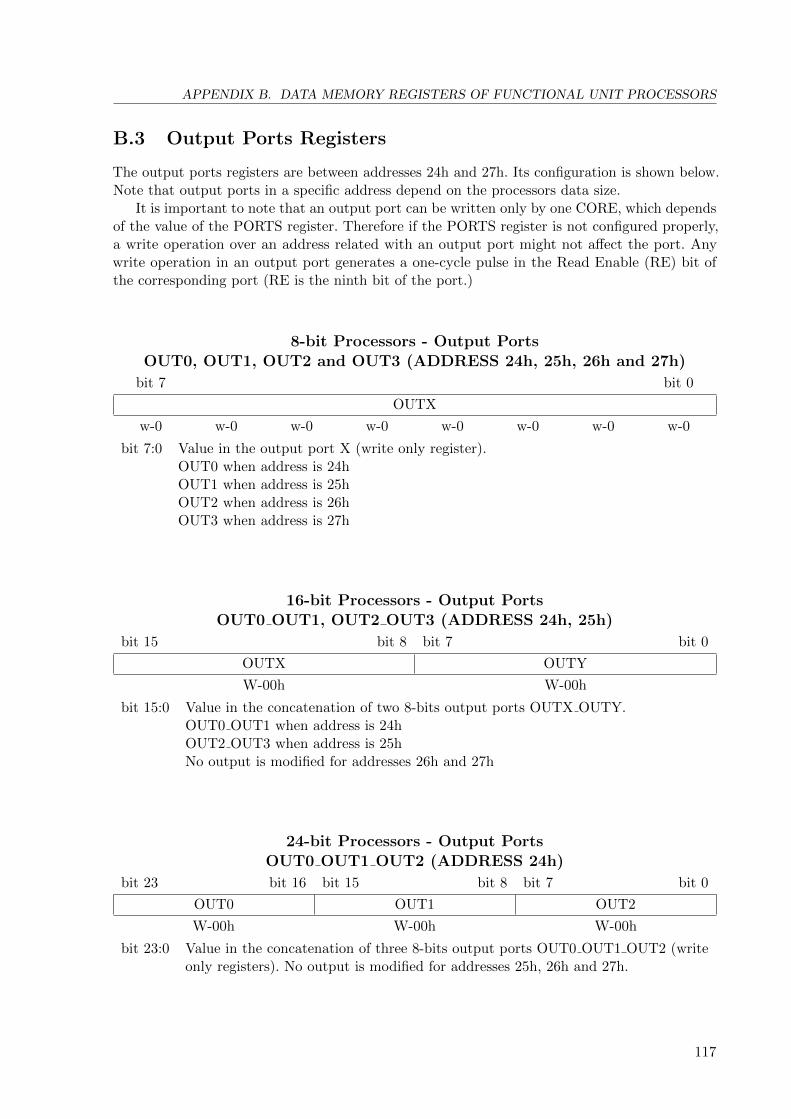
APPENDIX B. DATA MEMORY REGISTERS OF FUNCTIONAL UNIT PROCESSORS
B.3 Output Ports Registers
The output ports registers are between addresses 24h and 27h. Its configuration is shown below.Note that output ports in a specific address depend on the processors data size.
It is important to note that an output port can be written only by one CORE, which dependsof the value of the PORTS register. Therefore if the PORTS register is not configured properly,a write operation over an address related with an output port might not affect the port. Anywrite operation in an output port generates a one-cycle pulse in the Read Enable (RE) bit ofthe corresponding port (RE is the ninth bit of the port.)
8-bit Processors - Output PortsOUT0, OUT1, OUT2 and OUT3 (ADDRESS 24h, 25h, 26h and 27h)
bit 7 bit 0
OUTX
w-0 w-0 w-0 w-0 w-0 w-0 w-0 w-0
bit 7:0 Value in the output port X (write only register).OUT0 when address is 24hOUT1 when address is 25hOUT2 when address is 26hOUT3 when address is 27h
16-bit Processors - Output PortsOUT0 OUT1, OUT2 OUT3 (ADDRESS 24h, 25h)
bit 15 bit 8 bit 7 bit 0
OUTX OUTY
W-00h W-00h
bit 15:0 Value in the concatenation of two 8-bits output ports OUTX OUTY.OUT0 OUT1 when address is 24hOUT2 OUT3 when address is 25hNo output is modified for addresses 26h and 27h
24-bit Processors - Output PortsOUT0 OUT1 OUT2 (ADDRESS 24h)
bit 23 bit 16 bit 15 bit 8 bit 7 bit 0
OUT0 OUT1 OUT2
W-00h W-00h W-00h
bit 23:0 Value in the concatenation of three 8-bits output ports OUT0 OUT1 OUT2 (writeonly registers). No output is modified for addresses 25h, 26h and 27h.
117

B.3. OUTPUT PORTS REGISTERS
32-bit Processors - Output PortsOUT0 OUT1 OUT2 OUT3 (ADDRESS 24h)
bit 31 bit 24 bit 23 bit 16 bit 15 bit 8 bit 7 bit 0
OUT0 OUT1 OUT2 OUT3
W-00h W-00h W-00h W-00h
bit 31:0 Value in the concatenation of four 8-bits output ports OUT0 OUT1 OUT2 OUT3(write only registers). No output is modified for addresses 25h, 26h and 27h. PORTSregister must be set to E4h.
118

APPENDIX B. DATA MEMORY REGISTERS OF FUNCTIONAL UNIT PROCESSORS
B.4 Code Condition Register
The Code Condition Register (CCR) contains the arithmetic status of the ALU and the statusof the thread executed. The CCR register can be read by any instruction, as with any otherregister.
The Z and C elements correspond to the flags that indicate when an operation is zero andwhen the operation has a carry respectively. These bits indicate the results of the instructionjust executed. The Carry bit can be modified using the instructions CLC and SEC.
The bit TA (Thread Active) indicates if the execution thread has finished or not. Theinstruction END is the only one able to stop the execution of the thread (TA ← 0).
For 16, 24 and 32 bit processors, the most significant bits of CCR (from the bit 8) must beassumed as unimplemented, a read operation will return 0’s.
Condition Code Register - CCR (ADDRESS 28h)
bit 7 bit 0
- - - - - TA Z C
u-0 u-0 u-0 u-0 u-0 r-0 r-0 r-0
bit 7:3 Unimplemented.
bit 2 TA - Thread Active1 = Thread is active.0 = Thread not active. The END instruction is the only that can stop a thread(TA← 0).
bit 1 Z - Zero bit1 = The result of a logic or arithmetic operation is zero.0 = The result of a logic or arithmetic operation is not zero.
bit 0 C - Carry bit1 = The result of a shift, logic or arithmetic operation generates a carry bit.0 = No carry.
119

B.5. MODE REGISTER
B.5 Mode Register
The Mode register configures the operation mode of the FU. In other words, it configuresthe number of processors in the cell and specifies the configuration of the Data and ProgramMemories.
The FU may have 1 to 4 processors. The FU can be configured for data processing of 8, 16,24 and 32 bits, and the thread capacity can be for 64, 128, 192 or 256 instructions.
This register is loaded for the CµP in prototype when a new cell is inserted. For 16, 24and 32 bit processors, the most significant bits of MODE (from the bit 8) must be assumed asunimplemented, a read operation will return 0’s.
Mode Register - MODE (ADDRESS 29h)
bit 7 bit 0
- - - - mode
u-0 u-0 u-0 u-0 r-0 r-0 r-0 r-0
bit 7:4 Unimplemented.
bit 3:0 mode: Specifies the Configuration Mode (CM) of cores in Functional Unit.
0000 = CM 0: four processors [P0: 8x8, 64] [P1: 8x8, 64] [P2: 8x8, 64] [P3: 8x8, 64]
0001 = CM 1: three processors [P0: 16x8, 128] [P2: 8x8, 64] [P3: 8x8, 64]
0010 = CM 2: two processors [P0: 16x8, 128] [P2: 16x8, 128]
0011 = CM 3: two processors [P0: 24x8, 192] [P3: 8x8, 64]
0100 = CM 4: one processors [P0: 32x8, 256]
0101 = CM 5: three processors [P0: 8x16, 128] [P2: 8x8, 64] [P3: 8x8, 64]
0110 = CM 6: two processors [P0: 8x16, 128] [P2: 16x8, 128]
0111 = CM 7: two processors [P0: 8x16, 128] [P2: 8x16, 128]
1000 = CM 8: two processors [P0: 8x16, 192] [P2: 16x8, 64]
1001 = CM 9: one processors [P0: 16x16, 256]
1010 = CM 10: two processors [P0: 8x24, 192] [P3: 8x8, 64]
1011 = CM 11: one processors [P0: 8x32, 256]
others = Configuration mode not implemented
Note: [P0: 16x8, 64] = [Processor 0: General Purpose Registers with 16 words of 8 bits eachmapped in Data Memory, Program Memory with capacity for 64 instructions]
120

APPENDIX B. DATA MEMORY REGISTERS OF FUNCTIONAL UNIT PROCESSORS
B.6 Family Register
The Family register is reserved for future implementations. This register has been reserved forsupporting the implementation of microthreads.
This register is loaded for the CµP in prototype when a new cell is inserted.
Family Register- FAMILY (ADDRESS 2Ah)
bit 7 bit 0
FAMILY
r-0 r-0 r-0 r-0 r-0 r-0 r-0 r-0
bit 7:0 Family ID of thread.
121

B.7. OUTPUT PORTS CONFIGURATION REGISTER (PORTS)
B.7 Output Ports Configuration Register (PORTS)
This register configures the CORE that may perform a write operation over any output portof the FU i.e. select the ALU of a CORE that writes the result of any operation to the OUTXregister.
For 16, 24 and 32 bit processors, the most significant bits of PORTS (from the bit 8) mustbe assumed as unimplemented, a read operation will return 0’s.
The value of some PORTX field could be disabled when the FTS is enabled in the redundantcell (see FTCSR in section B.9).
This register is loaded for the CµP in prototype when a new cell is inserted.
Output Ports Configuration Register - PORTS (ADDRESS 2Bh)
bit 7 bit 0
PORT3 PORT2 PORT1 PORT0
r-1 r-1 r-1 r-0 r-0 r-1 r-0 r-0
bit 7:6 PORT3: Sets the core that can performs write operations in the OUT3.
00 = OUT3 can be written from CORE0
01 = OUT3 can be written from CORE1
10 = OUT3 can be written from CORE2
11 = OUT3 can be written from CORE3
bit 5:4 PORT2: Sets the core that can performs write operations in the OUT2.
00 = OUT2 can be written from CORE0
01 = OUT2 can be written from CORE1
10 = OUT2 can be written from CORE2
11 = OUT2 can be written from CORE3
bit 3:2 PORT1: Sets the core that can performs write operations in the OUT1.
00 = OUT1 can be written from CORE0
01 = OUT1 can be written from CORE1
10 = OUT1 can be written from CORE2
11 = OUT1 can be written from CORE3
bit 1:0 PORT0: Sets the core that can performs write operations in the OUT0.
00 = OUT0 can be written from CORE0
01 = OUT0 can be written from CORE1
10 = OUT0 can be written from CORE2
11 = OUT0 can be written from CORE3
122

APPENDIX B. DATA MEMORY REGISTERS OF FUNCTIONAL UNIT PROCESSORS
The next are sample values for PORTS register, each value depends of configuration mode,e.g., if MODE=00h and PORTS=E4h, the processor 0 (P0) can write any value to OUT0, P1 toOUT1, P2 to OUT2 and P3 to OUT3. In this case, if P0 performs a write operation over OUT1,OUT2 or OUT3, these registers will not be affected.
MODE PORTS P0 P1 P2 P3
00h E4h OUT0 OUT1 OUT2 OUT3
01h E0h OUT0, OUT1 - OUT2 OUT3
02h A0h OUT0, OUT1 - OUT2, OUT3 -
03h C0h OUT0, OUT1, OUT2 - - OUT3
04h 00h OUT0, OUT1, OUT2, OUT4 - - -
05h E4h OUT0 OUT1 - OUT2 OUT3
06h A4h OUT0 OUT1 - OUT2, OUT3 -
07h E4h OUT0 OUT1 - OUT2 OUT3 -
08h F4h OUT0 OUT1 - - OUT2, OUT3
09h 44h OUT0 OUT1, OUT2 OUT3 - - -
0Ah E4h OUT0 OUT1 OUT2 - - OUT3
0Bh E4h OUT0 OUT1 OUT2 OUT3 - -
- Denotes that the processor is unimplemented.
, Denotes output registers in different addresses.
Denotes concatenation of two or more output registers.
123

B.8. SUBPROCESS CONFIGURATION AND STATUS REGISTER (SUBPCSR)
B.8 Subprocess Configuration and Status Register (SUBPCSR)
This register controls the execution of subprocesses in the system.For 16, 24 and 32 bit processors, the most significant bits of SUBPCSR (from the bit 8) must
be assumed as unimplemented, a read operation will return 0’s.
Subprocess Configuration and Status RegisterSUBPCSR (ADDRESS 2Ch)
bit 7 bit 0
SWS ESP3 ESP2 ESP1 ESP0 SUBPID EXSP
r-0 w/r-0 w/r-0 w/r-0 w/r-0 w/r-0 w/r-0 w/r-0
bit 7 SWS - SYSTEM WAIT STATE: The SYSTEM is in wait state. The GCU ofthe master chip could receive subprocess instructions. This bit is controlled by CCU.1 = SYSTEM in wait state. This bit is set when the CCU receives a frame thatcontains a command related to the state wait.0 = SYSTEM is not in wait state. When a processor sets EXSP bit to high level orwhen a cell receives any data from INET, this bit is set to zero automatically.
bit 6 ESP3 - ENDS SUBPROCESS 3: The execution of the subprocess 3 has ended.The CCU sets this bit, but must be cleared by software.1 = Creation of subprocess 3 end.0 = No creation.
bit 5 ESP2 - ENDS SUBPROCESS 2: The execution of the subprocess 2 has ended.The CCU sets this bit, but must be cleared by software.1 = Creation of subprocess 2 end. CCU sets this bit. It must be cleared by software.0 = No creation.
bit 4 ESP1 - ENDS SUBPROCESS 1: The execution of the subprocess 1 has ended.The CCU sets this bit, but must be cleared by software.1 = Creation of subprocess 1 end.0 = No creation.
bit 3 ESP0 - ENDS SUBPROCESS 0: The execution of the subprocess 0 has ended.The CCU sets this bit, but must be cleared by software.1 = Creation of subprocess 0 end.0 = No creation.
bit 2:1 SUBPID - SUBPROCESS ID: ID of the subprocess to execute.00 = Subprocess 0.01 = Subprocess 1.10 = Subprocess 2.11 = Subprocess 3.
bit 0 EXSP - EXECUTE SUBPROCESS: Executes a subprocess for a specific com-ponent.1 = The FU sends a command indicating to execute a subprocess of the componentto which the cell belongs.0 =No execute.
Note: when using the instruction MOVLF for writing this register, be sure to configure appro-priately the destination (d=0), otherwise you may modify the register value.
124

APPENDIX B. DATA MEMORY REGISTERS OF FUNCTIONAL UNIT PROCESSORS
B.9 Fault Tolerance Configuration and Status Register (FTCSR)
This register configures the Fault Tolerance System (FTS).
For 16, 24 and 32 bit processors, the most significant bits of FTCSR (from the bit 8) mustbe assumed as unimplemented, a read operation will return 0’s.
This register is loaded for the CµP in prototype when a new cell is inserted.
Fault Tolerance Configuration and Status RegisterFTCSR (ADDRESS 2Dh)
bit 7 bit 0
FTEF FTE - FTRC ft mode
r-0 r-0 u-0 r-0 r-0 r-0 r-0 r-0
bit 7 FTEF - FAULT TOLERANCE ERROR FLAG: The FT error flag indicateswhen the FTS found an error while performing the comparison between two processors.1 = A FT error was detected, self-elimination and self-replication processes start.0 = no FT error.
bit 6 FTE - FAULT TOLERANCE ENABLE: Enables or disables the FTS.1 = FTS enabled.0 = FTS disabled.
bit 5 Unimplemented.
bit 4 FTRC - FAULT TOLERANCE REDUNDANT CELL: Indicates if the cellis the redundant cell, this bit should be set in ft modes = 5, 6, 7 and 8. The databus of a core is connected to output ports directly i.e. some bits of PORTS registerare disabled, RE is set to ’1’.1 = Redundant cell. It automatically disables the comparators of FTS for this cell.
FT mode 5: The CORE0 writes permanently the OUT0 (C0⇒OUT0).PORT0 disabled (P0-D).
FT mode 6: C0⇒OUT0, C1⇒OUT1. [P0,P1]-D.FT mode 7: C0⇒OUT0, C1⇒OUT1, C2⇒OUT2. [P0,P1,P2]-D.
FT mode 8: C0⇒OUT0, C1⇒OUT1, C2⇒OUT2, C3⇒OUT3. [P0,P1,P2,P3]-D.
0 = Primary cell.
bit 3:0 FT MODE: Specifies the fault tolerance configuration mode.
0000 = FT mode 0: [C0 ⇔ C1]
0001 = FT mode 1: [C0 ⇔ C1] & [C2 ⇔ C3]
0010 = FT mode 2: [C2 ⇔ C3]
0011 = FT mode 3: [C0 ⇔ C2]
0100 = FT mode 4: [C0 ⇔ C2] & [C1 ⇔ C3]
0101 = FT mode 5: [C0 ⇔ C0*]
0110 = FT mode 6: [C0 ⇔ C0*] & [C1 ⇔ C1*]
0111 = FT mode 7: [C0 ⇔ C0*] & [C1 ⇔ C1*] & [C2 ⇔ C2*]
1000 = FT mode 8: [C0 ⇔ C0*] & [C1 ⇔ C1*] & [C2 ⇔ C2*] & [C3 ⇔ C3*]
others = FT configuration mode not implemented
Note: Symbol ⇔ indicates comparison between CORES (C). *Denote a CORE in the redundantcell. The connections must be implemented by user.
125


Appendix C
Flow Diagrams for Self-adaptiveProcesses in System
Sports do not build character. They reveal it.
El deporte no construye el caracter. Lo revela.
Haywood Hale Broun (1918 – 2001)
Abstract: This chapter presents the flow diagrams of self-adaptive algorithms included in
the system. These algorithms are implemented in the Configuration Units of Cell and Switch
Matrix. The flow diagrams presented include the algorithms for self-placement, self-routing
and self-derouting processes.
Along this chapter, the labels “ inet” and “ enet” will be added to differentiate frames thatincludes commands related with the Internal Network (INET) and External Network (ENET)respectively.
C.1 Transmission and Reception in Cell
The transmission and reception processes used for the Cell Configuration Unit (CCU) are shownin Figure C.1. The CCU implements these algorithms for the communication with the GlobalConfiguration Unit (GCU) thought INET. The communication protocol and interface communi-cation are explained in detail in sections 2.11 and 2.12. These processes participate actively inthe self-routing and self-placement algorithms.
The data in frames is divided in four groups. The first group (tx control = 00) sends between1 and 256 bytes of information, using the nBytes field for specifying the number of bytes. Thesecond group (tx control = 01) only sends the command, it does not send arguments. The thirdgroup are the commands that use the acknowledge bit (tx control = 10) and the last group(tx control = 11) use the transmission and reception to perform a comparison process of data(8-bits).
When the CCU requires the acknowledge bit, the transmission process always sends a logic‘1’ in the time space of the acknowledge bit, and the reception process performs simultaneouslythe read and write of the acknowledge bit. It is important to note that all the cells in the arrayparticipate in this process, but only one can write the acknowledge bit with a logic ‘0’, the cellwhich address match with the address field of the frame.
It is possible that several CCUs require the comparison of a special number to take anyaction, in this case the CCUs send the control bits (11), the associated command (scan . . . ) and
127

C.2. SELF-PLACEMENT PROCESSES IN CCU
Stanby
yes
no
yestx_controlh=h00?
no
tx_controlh=h10?
Sendhbytehtx_nByteshand1htoh256hbyteshofhdata.
tx_controlh=h01,hnoharguments
Thehrxhprocesshsetsthehacknowledgementhbit
Sendhonehbit:hlogichH1H
no
no
tx_controlh=h11?Sendshonehbyte,hthatcorrespondshtohthecomparisonhbyte.
yes
yes
tx_starth=h1?
Startshatransmissionhprocess
Sendhstarthcondition.SendhHeader.
Sendhstophcondition.
Thehbitshtransmitedhcouldhbesethtoh1hbyhthehcomparison
processhthathishbeingsimultanouslyhexecuted
inhthehrxhprocess.
(a) TX process.
ReceiveGheaderM
Stanby
yes
no
Data
AcknowledgeGbit
Comparisonbyte
yes no
TheGsourceGcellGreadstheGacknowledgeGbitM
,targetGcellFGeneratesGthe
acknowledgmentGbitM
startconditiondetected?
yes
no
rx_controlG=GPP?yes
no
no
stopconditiondetected?
no
no
yes
no
ReceivesGandGstoresGdatadependingGofGtheGcommandM
Data:Gaddress_temp2GconnectionGtable2FU_program_memories_,P2G12G22G3F2cofigurationsGregistersGorGotherGdataM
MainlyGforGtheGcommands:insert_first_cell2Ginsert_otherGcell2
write_program_memory_,P2G12G22G3FandGwrite_configuration_register
ExecutionGofGtheComparisonGProcessM
ForGcommands:compare_first_cell2
compare_new_cell_connections2andGcompare_affinity_valueM
addressmatches?
rx_controlG=G11?
rx_controlG=G1P?
rx_controlG=G1P?
yes
yes
(b) RX process
Figure C.1: Transmission and reception processes in Cell Configuration Unit.
the comparison byte. The reception process performs the simultaneous comparison of the data.The winner is the cell that has the lowest comparison value, in case of a tie, the winner will bethe leftmost uppermost cell in the array.
C.2 Self-Placement Processes in CCU
C.2.1 Flow Diagram for Insertion of First Cell of a Component
Figure C.2 shows a detailed description of the algorithm implemented by cells for the insertionprocess of the first cell of a component. The process is started by GCU who sends the commandinsert first cell inet with the address and connection tables of the new cell as arguments. Theprocess ends when the GCU receives the command end first cell inet.
C.2.2 Flow Diagram for Insertion of Other Cells of a Component
The process is started by GCU who sends the command insert other cell inet with the addressand connection tables of the new cell as arguments. The flow diagram of the algorithm thatperforms the self-placement of the other cells of the component (from the second) is shown inFigure C.3.
It is important to note, that after the placement process, the self-routing process at cell levelstarts. The self-placement and self-routing processes ends when the GCU receives the commandend other cell inet (Figure C.4).
128

APPENDIX C. FLOW DIAGRAMS FOR SELF-ADAPTIVE PROCESSES IN SYSTEM
Read,Command-cmdp
busy,cell?yes
no
Stanby
yes
Winningcell?
Set,as,busy,cell.Send,confirmation:
tx,command,<=,end_first_cellItx_byte-0:3p,<=,address.
yes
Delete,addressand
connection,tables.
Receivenew,data?
yes
no
no
The,SelfAplacement,of,the,first,cellof,a,component,ends,succesfully.
store,adddress:,rx_byte-0:3p.Start,a,comparison,process:
tx_control,<=,3comparison,byte3Itx,command,<=,compare_first_cellI
tx_byte0,<=,congestion,+,busy,neighbor,cells.
Congestion,is,thenumber,of,remote,ports
busy,or,not,available
yes
busy,cell?
yesyes
If,is,nota,busy,cellI
the,connectiontables,was
stored,by,therx,process.
no
no
cmd,=compare_first
_cell?
cmd,=insert_first_cell?
cmd,=end_first_cell
no
no
A,stop,condition,wasreceived,in,rx_process. broadcast
Figure C.2: Self-placement algorithm for the insertion of the first cell of a component.
ReadxCommand,cmdB
Stanby
busyxcell?yes yes
cellxofxsamecomponent?
calculatexthexnumberxofxconnectionswithxthexnewxcell:
new_cell_connections_numberyes
addressx<=address_temp
no
Calculatexthemanhatanxdistancewithxothersxcells.yes
no
busyxcell?no
,StartxaxcomparisonxprocessB.tx_controlx<=xvcomparisonxbytev.
txxcommandx<=xcompare_affinity_value.tx_byte0:xaffinity.
Winningxcell?
Setxasxbusyxcell.SetxasxsourcexcellxforxselfProutingxprocess.
deletexaddressxandconnectionxtable
yes
no
yes
yes
no
Ifxisxnotxaxbusycellkxthe
rxxprocessstoresxthe
connectionxtable.
,StartxaxcomparisonxprocessBtx_controlx<=xvcomparisonxbytev.
txxcommandx<=xcompare_new_cell_connectionstx_byte0x<=xnew_cell_connections_number
,BroadcastxaxmessageBtxxcommandx<=xrequest_compare_affinity_value.
yes
yes
yes
EndsxsuccesfullyxthexSelfPplacementxprocessxforxthexnewxcellxofxaxcomponent.
busyxcell?no
yes
nono
Winningcell?
Receivenewxdata?
Checksxthexid_componentfieldxofxthexaddress
cmdx=insert_other
_cell?
cmdx=request_compare_
affinity_value?
cmdx=compare_affinity
_value?
broadcast
broadcast
no
no
no
cmdx=compare_new_cell_
connections?
Processxtoxconfigurexthexsourceandxtargetxcellskxforxroutingxallxpossibleconnectionsxwithxthexnewxinsertedxcell.
Figure C.3: Self-placement algorithm for other cells of a component (from the second).
129

C.3. SELF-ROUTING PROCESSES IN CCU
C.3 Self-Routing Processes in CCU
C.3.1 Flow Diagram to select the Source and Target cells before the Expan-sion Process at Cell Level
The algorithm presented in Figure C.4 is executed after the insertion of the remaining cells of acomponent (from the second). Note that the process starts when the self-placement algorithmpresented in Figure C.3 ends.
When the source cell and target cell are ready to configure a connection, the source cellstarts the “Expansion Process at Cell Level”. For this purpose the flag Starts Cell Propagationis used.
Read_Command,cmdp
Stanby
yes
no
no
x_<=_x_P_W
no
Set_as_target_cell
yes
no
yes
no
Reset_as_target_cell
x_<=_Lno
yes
End_of_table?
no
Reset_as_source_cellA_tx_control_<=_DDataDAtx_command_<=_connect_others_to_new_celltx_byte,LAA3p_<=_address_of_new_inserted_cell
yes
yes
If_the_address_matchesTthe_Data_Reception
process_generates_theacknowledgement_bit
yes
Set_as_target_cellyes
Reset_as_target_cell
no
yesPossibles
source_cellsA
Start_theelimination
process
yes
yes
tx_control_<=_DDataDtx_command_<=_end_other_cellAtx_byte,LAA3p_<=_rx_byte,LAA3pA
no
no
The_Self-placement_andself-routing_processesof_the_new_inserted_cell
of_a_component_wascompleted_succesfully
The_new_inserted_cellwas_set_as_source_cellfor_self-routing_process
Set_as_source_cellAx_<=_L
x_<=_x_P_W
End_of_table?
yes
no
Reset_as_source_cellAtx_control_<=_DDataDA
tx_command_<=_connect_others_to__new_celltx_byte,LAA3p_<=_address_of_new_inserted_cell
yes
no
tx_control_<=_DAcknowledge_bitDAtx_command_<=_set_target_cell_srAtx_address_<=_output_connection,xpReceive
new_data?
cmd_=set_target_cell_sr?
sourcecell?
cell_of_samecomponent?
Any_cell_has_at_leastone_connection_not-routed_with
the_new_inserted_cell?
output_connection,xpis_with_the_new_inserted
cell?
output_connection,xpbelong_to_same
component?
acknowledgereceived?
cmd_=connect_others_to
_new_cell?
cmd_=end_other
_cell?
no
yes
address_=rx_address
Leftmostuppermost
cellA
Winningcell?
broadcast
broadcast
Process_to_configure_the_sourceand_target_cellsT_for_routing_all_possibleconnections_with_the_new_inserted_cellA
address_=rx_byte,LAA3p
yes
no
no
Starts_Cell_Propagation,Starts_the_ExpansionProcess_at_Cell_Levelp
Starts_Cell_Propagation,Starts_the_ExpansionProcess_at_Cell_Levelp
Figure C.4: Configuration of source and target cell for execution of Expansion Process at CellLevel.
130

APPENDIX C. FLOW DIAGRAMS FOR SELF-ADAPTIVE PROCESSES IN SYSTEM
C.3.2 Main Flow Diagram in CCU
Figure C.5 shows the flow diagram for the Expansion and Release processes in Cell ConfigurationUnit (CCU). This is the start point for the execution of any process in system that requiresthe propagation of signals using the expansion ports of cells, SMs and PIMs. It includes theExpansion at Cell or Component level and the Release processes.
The flow diagram remains in standby state until the CCU of a cell in the array starts one ofthe following process:
1. Expansion Process at Cell Level (Search Phase): this process is started by the source cellwhen the signal start cell propagation is set.
2. Expansion Process at Component Level (Search Phase): this process is started by the sourcecell when the signal start component propagation is set.
3. Expansion Process at Component Level (Search Phase): this process is started by the sourcecell when the signal start component propagation pin is set.
4. Release Process: this process is started by the target cell when the signal start delete cellconnection is set.
The cells on the array that receive any propagation signals can execute any of the processdenoted with a box in the figure, as follows:
1. Neighbor [NORTH, EAST, SOUTH or WEST]: The process is executed when a neighbor in Xsignal is received. These boxes represent the transition between the Search and ConfigurationPhases of the Expansion Process at Cell Level when the target cell is reached in a neighborcell.
2. Propagate [NORTH, EAST, SOUTH or WEST]: The process is executed when a propagate inX signal is received. These boxes represent the transition between the Search and ConfigurationPhases of the Expansion Process at Cell Level when the target cell is reached.
3. Propagate Matrix: The process is executed when a propagate in matrix signal is received. Thisbox represents the transition between the Search and Configuration Phases of the ExpansionProcess at Component Level when the target cell is reached.
4. Delete [NORTH, EAST, SOUTH or WEST]: The process is executed when a del connectionin X signal is received. These boxes represent a step in the Release Process at Cell Level.
5. Delete Matrix: The process is executed when a del connection in matrix signal is received.This box represents the end of the Release Process at Component Level.
6. Expansion Process at Cell Level - Configuration Phase [NORTH, EAST, SOUTH or WEST]:The process is executed when the cell is in lock cell state and a lock in X signal is received.These boxes represent the Configuration Phase of the Expansion Process at Cell Level.
131

C.3. SELF-ROUTING PROCESSES IN CCU
stateR=standby?
yesno
EvaluateRState
startRcellpropagation?
yes
no
ExpansionRProcessatRCellRLevel
kSearchRPhaseD
NeighborNORTH
PropagateNORTH
startRcomponetpropagation?
yes
no
id_target_port_outR<=RCT_target_port;id_source_port_outR<=RCT_source_port;
propagate_out_matrixR<=RF;
stateR<=Rlock_component
startRcomponetpropagationRpin?
yes
no
id_target_port_outR<=Rid_target_pin;id_source_port_outR<=RCT_source_port;
propagate_out_matrixR<=RF;
stateR<=Rlock_component
startRdeletecellRconnection?
yes
StartRReleaseProcess
DeleteNORTH
DeleteEAST
DeleteSOUTH
DeleteWEST
NeighborEAST
NeighborSOUTH
NeighborWEST
PropagateEAST
PropagateSOUTH
PropagateWEST
PropagateMATRIX
no
stateR=lock_cell?
yesno
ExpansionRProcessatRCellRLevel
kConfigurationRPhaseDNORTH
stateR=lock_component?
yes
no
lock_in_matrix=F? stateR<=Rset_routing_complete
stateR=idle? yes
no
stateR<=Rstandbyrouting_complete_in=F?
yes
yes
no
no
stateR=set_routing_complete?
yes
no
stateR<=Rstandbyrouting_complete_outR<=RF
SELF_ROUTINGRinRCCU
SetRflagRforRconnectionkxDinROutputRConnectionRTable
stateR=set_derouting_complete?
yes
no
stateR<=Rstandbyrouting_complete_outR<=RF
ExpansionProcess
ComponentLevel
ReleaseRProcessIsignalRreceived:
del_connection_in_X
ExpansionRProcessRatCellRLevelRkSearchRPhaseD
signalRreceived:neighbor_in_X
ExpansionRProcessRatCellRLevelRkSearchRPhaseD
signalRreceived:propagate_in_X
ExpansionRProcessatRCellRLevel
kConfigurationRPhaseDEAST
ExpansionRProcessatRCellRLevel
kConfigurationRPhaseDSOUTH
ExpansionRProcessatRCellRLevel
kConfigurationRPhaseDWEST
signalRreceived:Rlock_in_X
del_connection_in_matrix=F?
stateR<=Rset_derouting_complete
yes
no
DeleteMATRIX
Figure C.5: Main flow diagram for Expansion and Release processes in Cell Configuration Unit.
132

APPENDIX C. FLOW DIAGRAMS FOR SELF-ADAPTIVE PROCESSES IN SYSTEM
C.3.3 Expansion Process at Cell Level - Search Phase
The search phase is started by the source cell . This is an expansion process that propagatessignals in the sides of the cell that have available routing resources, like local and/or remote freeports. The propagation process includes the configuration of signals for each side (north, east,south and west) of the cell as shown in Figure C.6.
West
local2portN02used?
local_port_out_N2<=20;neighbor_out_N2<=21;
local_port_out_N2<=20;neighbor_out_N2<=21;
no
no
yes
yes
local2portN12used?
source2cellflag2=21?
yes
South
local2portN02used?
local_port_out_N2<=20;neighbor_out_N2<=21;
local_port_out_N2<=20;neighbor_out_N2<=21;
no
no
yes
yes
local2portN12used?
East
local2portN02used?
local_port_out_N2<=20;neighbor_out_N2<=21;
local_port_out_N2<=20;neighbor_out_N2<=21;
no
no
yes
yes
local2portN12used?
North
local2portN02used?
local_port_out_N2<=20;neighbor_out_N2<=21;
local_port_out_N2<=20;neighbor_out_N2<=21;
no
no
yes
yes
local2portN12used?
West
remote2portN02used?
remote_port_out_N2<=20;propagate_out_N2<=21;
remote_port_out_N2<=21;propagate_out_N2<=21;
no
yes
yes
remote2portN12used?
no
yes
remote2portN22used?
no
remote_port_out_N2<=22;propagate_out_N2<=21;
South
remote2portN02used?
remote_port_out_N2<=20;propagate_out_N2<=21;
remote_port_out_N2<=21;propagate_out_N2<=21;
no
yes
yes
remote2portN12used?
no
yes
remote2portN22used?
no
remote_port_out_N2<=22;propagate_out_N2<=21;
East
remote2portN02used?
remote_port_out_N2<=20;propagate_out_N2<=21;
remote_port_out_N2<=21;propagate_out_N2<=21;
no
yes
yes
remote2portN12used?
no
yes
remote2portN22used?
no
remote_port_out_N2<=22;propagate_out_N2<=21;
North
remote2portN02used?
remote_port_out_N2<=20;propagate_out_N2<=21;
remote_port_out_N2<=21;propagate_out_N2<=21;
no
yes
yes
remote2portN12used?
no
yes
remote2portN22used?
no
remote_port_out_N2<=22;propagate_out_N2<=21;
id_target_port_out2<=2CT_target_portLxv
state2<=2lock_cell
no
Expansion2Process2at2Cell2Level2LSearch2Phasev
Figure C.6: Flow diagram for the propagation of Signals in the Search Phase of the ExpansionProcess at Cell Level.
Note that propagation of neighbor out X signal is only available for source cell when localports are available. The source cell and the other cells that participate in the Search Phase usethe propagate out X signal when remote ports are available.
When the target cell is a neighbor cell, the Search Phase ends and the Configuration Phasestarts as shown in Figures C.7a and C.7c. Note that these figures show the case for a propagationsignal received from NORTH. Similar functionality must be assumed for EAST, SOUTH andWEST.
When the target cell is not a neighbor cell, the propagation (C.6) is executed by each cellthat reads the propagate in X signal as shown in Figure C.7c. The priority order for propagationsignals is NORTH, EAST, SOUTH and WEST. The origin register stores the side from whichthe propagation signal was received. The propagation process explores the entire cell array untilfinding the target cell , if possible. The Configuration Phase starts when the Search Phase findsthe target cell .
133

C.3. SELF-ROUTING PROCESSES IN CCU
SimilarpforpEast,pSouthpandpWest
neighbor_in_N=1pandtarget_cell_flag=1?
yes
lock_out_Np<=p1;neighbor_out_Np<=p1;
local_port_out_Np<=plocal_port_in_N;
ConfigurepmuxpforpanyFUpinputpdependingpof:
local_port_in_Npandid_target_port_in_N
statep<=pidle
no
Neighborp-pNORTH
(a) Propagation signal at cell level for a neighbor cell.
propagate_in_matrix=1?
yes
lock_out_matrix-<=-1;
Configure-mux-for-anyFU-input-depending-of:
mux_id_matrix-andid_target_port_in_matrix
state-<=-idle
target_cell_flag=1?
yesno
no
Propagate---MATRIX
(b) Propagation signal at component level.
propagate_in_N=1?
yes
lock_out_N"<="1;remote_port_out_N"<="remote_port_in_N;
Configure"mux"for"anyFU"input"depending"of:remote_port_in_N"and
id_target_port_in_N
state"<="idle
target_cell_flag=1?
id_target_port_out"<="id_target_port_in_N;origin"<="RNORTHR;
Expansion"Processat"Cell"Level
vSearch"Phase(
yes
no
no
Similar"for"East)South"and"West
Propagate","NORTH
(c) Propagation signal at cell level.
Figure C.7: Flow diagrams for Expansion Process when propagation input signals is received inCell Configuration Unit.
134

APPENDIX C. FLOW DIAGRAMS FOR SELF-ADAPTIVE PROCESSES IN SYSTEM
C.3.4 Expansion Process at Cell Level - Configuration Phase
The Configuration Phase at Cell Level starts when the Search Phase finds the target cell (Fig-ures C.7a and C.7c).
The Configuration Phase that was started by the target cell goes backward over the pathpreviously configured in the Search Phase until it arrives to the source cell . This process configuresthe multiplexers of the corresponding cells to fix the path. The cells that participate in thisprocess are in the state lock cell and perform the actions described in Figure C.8 when thesignal lock in X in the corresponding side is activated. Similar functionality must be assumedfor EAST, SOUTH and WEST.
lock_in_N=1?
yes
lock_out_Ed<=d1;remote_port_out_Ed<=dremote_port_in_E;
Configuredmuxdforlocaldportdatdnorthdusign:
CT_source_portdandlocal_port_in_N
stated<=dset_routing_complete
source_cell_flag=1?
yes
no
no
SimilardfordEastHSouthdanddWest
ExpansiondProcessdatdCelldLeveld)ConfigurationdPhase-dbdNORTH
neighbor_in_N=1?
yes
Configuredmuxdforremotedportdatdnorthdusign:
CT_source_portdandremote_port_in_N
no
origin=,East,?
ConfiguredmuxdforremotedportdatdNORTHdusign:
remote_port_in_Edandremote_port_in_N
stated<=didle
OrigindbdEAST
OrigindbdSOUTH OrigindbdWEST
yesno
Figure C.8: Flow diagram for Configuration Phase of the Expansion Process at Cell Level.
135

C.3. SELF-ROUTING PROCESSES IN CCU
C.3.5 Release Process at Cell Level
This process releases the routing resources used for a interconnection between cells. The ReleaseProcess goes from the target to the source of a connection.
yes
no
STARTIRELEASEIPROCESS
stateI<=Iidle;
no
SetIfreeMux_FU_IN2
LocalIPortING
yes
no
LocalIPortIE2
LocalIPortIEG
LocalIPortIS2
LocalIPortISG
LocalIPortIW2
LocalIPortIWG
Mux_FU_IN2IisIconnectedwithIlocal_port_N2?
del_connection_out_NI<=IG;neighbor_out_NI<=IG;
local_port_OUT_NI<=I2;I[2[G]
LocalIPortIN2
Mux_FU_IN2IisIconnectedwithIremote_port_N2?
del_connection_out_NI<=IG;remote_port_OUT_NI<=I2;I[2[G[-]
RemoteIPortIN2
yes
no
RemoteIPortING
RemoteIPortIN-
RemoteIPortIE2
RemoteIPortIEG
RemoteIPortIE-
RemoteIPortIS2
RemoteIPortISG
RemoteIPortIS-
RemoteIPortIW2
RemoteIPortIWG
RemoteIPortIW-
FUITARGETIPORTI,IIN2
FUITARGETIPORTI,IING
FUITARGETIPORTI,IIN-
FUITARGETIPORTI,IIN3
FUITARGETIPORTI,IFT_IN2
FUITARGETIPORTI,IFT_ING
FUITARGETIPORTI,IFT_IN-
FUITARGETIPORTI,IFT_IN3
MatrixIMuxIYG
Mux_FU_IN2IisIconnectedwithImatrix_mux_Y2?
del_connection_out_matrixI<=IG;id_source_port_outI<=I2;I[2[G[-[3]
MatrixIMuxIY2
yes
noMatrixIMuxIY-
MatrixIMuxIY3
FUItarget_portI=IIN2?
Figure C.9: Flow digram of the start point of Release Process at Cell and Component Level.
136

APPENDIX C. FLOW DIAGRAMS FOR SELF-ADAPTIVE PROCESSES IN SYSTEM
If the connection is at cell level, the multiplexers of FU inputs, local and remote cell portsare released. In this case, the Release Process starts from the FU input port of the target cellan go backwards to the FU output port of the source cell . This process reads the multiplexersconfiguration and propagate the signal del connection out X in the direction where the connectionwas previously established by the self-routing process.
The target cell starts the process presented in Figure C.5 when the flag start delete cellconnection is set. Then, the target cell executes the algorithm presented in Figure C.9. There-after, each cell that receives the signal del connection in X executes the algorithm presented inFigure C.10 until it finds the source cell , which goes to the state set derouting complete and theprocess ends.
EvaluatebRemotebNORTHb:
EvaluatebRemotebNORTHbL
del_connection_in_N=L?
yes
stateb<=bset_derouting_complete
neighbor_in_N=L?
noSimilarbforbNFUbNLbandbN:
DeletebIbNORTH
remote_port_in_N=F?
no
yes
remote_port_in_N=L? remote_port_in_N=:?
yes yes yes
no no
stateb<=bERROR
SimilarbforbEastUbSouthbandbWest
no
Mux_Remote_NFconnectedbtoba
remotebportbatbEAST? yes
Setbremote_port_out_E;del_connection_out_Eb<=bL;
Mux_Remote_NFconnectedbtoba
remotebportbatbSOUTH?
Setbremote_port_out_S;del_connection_out_Sb<=bL;
SetbfreeMux_Remote_NF
Mux_Remote_NFconnectedbtoba
remotebportbatbWEST?
Setbremote_port_out_W;del_connection_out_Wb<=bL;
stateb<=bidle
stateb<=bset_derouting_complete
yes
yes
EvaluatebRemotebNORTHbF
no
no
no
Itbisbthebsourcebcell.Mux_Remote_NF
wasbconnectedtobabFUbOUTbport
local_port_in_N=F?
SetbfreeMux_Local_NF
SetbfreeMux_Local_NL
yes
no
Itbisbthebsourcebcell.Setbfreebmuxbfor
localbportbatNORTHbusign:local_port_in_N
Figure C.10: Flow digram of Release Process at Cell Level.
137

C.4. SELF-ROUTING PROCESSES IN SMCU
C.4 Self-Routing Processes in SMCU
When the Expansion or Release processes are at component level, the propagation of signalsis made between cells and SMs. Note that the process must be started and finalized by cells(Figure C.5) that propagate signals to the SM that belongs to the cluster, which in turn propagatessignals to the SMs of neighboring clusters until it finds the destination cell of a process.
Figure C.11 shows the flow diagram for the Expansion and Release processes in SwitchMatrix Configuration Unit (SMCU). It includes the Expansion at Cell or Component level andthe Release processes.
stateO=standby?
yesno
EvaluateOStatePropagate
CELLOA
DeleteCELLOA
DeleteCELLOB
DeleteCELLOC
DeleteCELLOI
PropagateCELLOB
PropagateCELLOC
PropagateOMatrixNORTH
stateO=lock_component?
yes
no
ExpansionOProcessatOComponentOLevel
(ConfigurationOPhasefCELLOA
stateO=idle? yes
no
stateO<=Ostandbyrouting_complete_in=.?
yes
no
SELF_ROUTINGOinOSMCU
ReleaseOProcessFsignalOreceived:
del_connection_in_cell_XorOdell_connection_in_X
ExpansionOProcessOatComponentOLevel(SearchOPhasefsignalsOreceived:
propagate_in_cell_XorOpropagate_in_X
ExpansionOProcessatOComponentlOLevel
(ConfigurationOPhasefCELLOB
ExpansionOProcessatOComponentlOLevel
(ConfigurationOPhasefCELLOC
ExpansionOProcessatOComponentlOLevel
(ConfigurationOPhasefCELLOI
signalOreceived:Olock_in_cell_X
PropagateCELLOI
PropagateOMatrixNORTHEAST
PropagateOMatrixEAST
PropagateOMatrixNORTHWEST
DeleteOMatrixNORTH
DeleteOMatrixNORTHEAST
DeleteOMatrixEAST
DeleteOMatrixNORTHWEST
ExpansionOProcessatOComponentOLevel
(ConfigurationOPhasefNORTH
ExpansionOProcessatOComponentlOLevel
(ConfigurationOPhasefNORTHEAST
ExpansionOProcessatOComponentOLevel
(ConfigurationOPhasefEAST
ExpansionOProcessatOComponentOLevel
(ConfigurationOPhasefNORTWEST
signalOreceived:Olock_in_X
Figure C.11: Main flow diagram for Expansion and Release processes in Switch Matrix Configu-ration Unit.
The SMCU remains in standby state until the CCU of a cell in the array starts one of thefollowing process:
1. Expansion Process at Component Level: this process is started by the source cell when thesignal start component propagation is set.
2. Expansion Process at Component Level: this process is started by the source cell when thesignal start component propagation pin is set.
138

APPENDIX C. FLOW DIAGRAMS FOR SELF-ADAPTIVE PROCESSES IN SYSTEM
3. Release Process at Component Level: this process is started by the target cell when the signalstart delete cell connection is set.
The SM that receives any propagation signals can execute any of the process denoted with abox in the figure, as follows:
1. Propagate CELL [A, B, C, D, E, F, G, H or I]: The process is executed when a propagate incell X signal is received. These processes correspond with the Search Phase of the ExpansionProcess at Component Level.
2. Propagate Matrix [NORTH, NORTHEAST, EAST, SOUTHEAST, SOUTH, SOUTHWEST,WEST or NORTHWEST]: The process is executed when a propagate in X signal is received.These processes correspond with the Search Phase of the Expansion Process at ComponentLevel.
3. Delete Cell [A, B, C, D, E, F, G, H or I]: The process is executed when a del connectionin cell X signal is received. These boxes correspond with the Release Process at componentlevel.
4. Delete Matrix [NORTH, NORTHEAST, EAST, SOUTHEAST, SOUTH, SOUTHWEST, WESTor NORTHWEST]: The process is executed when a del connection in X signal is received.These boxes correspond with the Release Process at component level.
5. Expansion Process at Component Level - Configuration Phase [A, B, C, D, E, F, G, H or I]:The process is executed when the SM is in lock component state and a lock in cell X signalis received.
6. Expansion Process at Component Level - Configuration Phase [NORTH, NORTHEAST,EAST, SOUTHEAST, SOUTH, SOUTHWEST, WEST or NORTHWEST]: The process isexecuted when the SM is in lock component state and a lock in X signal is received.
C.4.1 Expansion Process at Component Level - Search Phase
The search phase is started by the source cell (Figure C.5) with the signal propagate out matrix.The source cell goes to the lock component state waiting for the Configuration Phase. Theprocess continues at component level when the SM reads the signal propagate in cell X as shownin Figure C.12a, then the SM propagate signals until it finds the target cell . If the target cell isnot in the same cluster, the SM continues the Search Phase when it receives the propagationsignal propagate in X as shown in Figure C.12b. Note that these figures show the case for apropagation signal received from Cell A and SM at NORTH. Similar functionality must beassumed for other cells and other sides of SM.
The expansion process propagates signals in the sides of the SM that has available routingresources. The propagation process includes the configuration of signals for each side (north,northeast, east, southeast, south, southwest, west and northwest) of the SM and for each cell ofthe cluster (Cell A, Cell B, . . . Cell I ) as shown in Figure C.13.
The priority order for propagation signals is NORTH, NORTEAST, EAST, SOUTHEAST,SOUTH, SOUTHWEST, WEST and NORTHWEST. The origin cell and origin matrix registerstores the cell or the side from which the propagation signal was received. The propagationprocess explores the entire cell array until finding the target cell , if possible. The ConfigurationPhase starts when the Search Phase finds the target cell .
139

C.4. SELF-ROUTING PROCESSES IN SMCU
propagate_in_cell_A=1?
yes
id_target_port_out(<=(id_target_port_in_cell_A;origin_cell(<=(hCELL(Ah;
Expansion(Processat(Componet(Level
FSearch(PhaseG
no
Similar(for(Cells(B-(C-(D-(E-(F-(G-(H(and(I
Propagate(-(CELL(A
(a) Propagation signal from a Cell.
propagate_in_N=1?
yes
id_target_port_outC<=Cid_target_port_in_N;origin_matrixC<=CvNORTHv;
ExpansionCProcessatCComponetCLevel
fSearchCPhaseA
no
SimilarCforCConnectionCatCNORTEASTWCEASTWCSOUTHEASTSOUTHWCSOUTHWESTWCWESTCandCNORTHWEST
PropagateCMatrixCNORTH
(b) Propagation signal from a Switch Matrix.
Figure C.12: Flow diagrams for propagation input signals at component level in Switch MatrixConfiguration Unit.
CELLnI
CELLnH
CELLnG
CELLnF
CELLnE
CELLnD
CELLnC
CELLnB
NORTHWEST
WEST
SOUTHWEST
SOUTH
SOUTHEAST
EAST
NORTHEAST
staten<=nlock_component
no
ExpansionnProcessnatnComponentnLeveln)SearchnPhaseM
CELLnA
MuxnA1used?
mux_id_cell_An<=n1;propagate_out_cell_An<=ny;
noyes
MuxnAyused?
mux_id_cell_An<=ny;propagate_out_cell_An<=ny;
noyes
MuxnA2used?
mux_id_cell_An<=n2;propagate_out_cell_An<=ny;
noyes
MuxnA3used?
mux_id_cell_An<=n3;propagate_out_cell_An<=ny;
noyes
NORTH
matrixnportN1nused?
matrix_port_out_Nn<=n1;propagate_out_Nn<=ny;
rmatrix_port_out_Nn<=ny;propagate_out_Nn<=ny;
no
yes
yes
matrixnportNynused?
no
yes
matrixnportN2nused?
no
matrix_port_out_Nn<=n2;propagate_out_Nn<=ny;
Figure C.13: Flow diagram for the propagation of Signals in the Search Phase of the ExpansionProcess at Component Level.
140

APPENDIX C. FLOW DIAGRAMS FOR SELF-ADAPTIVE PROCESSES IN SYSTEM
C.4.2 Expansion Process at Component Level - Configuration Phase
The Configuration Phase at Component Level starts when the Search Phase finds the target cell(Figure C.5), in the process denoted as Propagate Matrix (Figure C.7b), then the multiplexer ofthe appropriate FU input port is configured (FU target port).
The Configuration Phase that was started by the target cell goes backward over the pathpreviously configured in the Search Phase until it arrives to the source cell . This process configuresthe multiplexers of the corresponding SMs to fix the path.
lock_in_cell_A=G?
yes
lock_out_cell_BL<=LG;
no
SimilarLforLCellLBLtoLCellLI
ExpansionLProcessLatLComponentLLevelLMConfigurationLPhaseXL:LCELLLA
origin_cell=(CellLB(?
ConfigureLMux_AXLforLconnectionbetweenLCellLALandLBLusign:
id_source_port_in_BLandmux_id_cell_A;
stateL<=Lidle
OriginL:LCellLB
yes
no
OriginL:LCellLC
OriginL:LCellLD
OriginL:LCellLE
OriginL:LCellLF
OriginL:LCellLG
OriginL:LCellLH
OriginL:LCellLI
OriginLinLCluster
originLisLfromLSMLport?
RegisterLorigin_cellinLvalueLFxF
isLusedLasLflag
matrix_port_out_NL<=Lmatrix_port_in_Nlock_out_NL<=LG;
origin_matrix=(NORTH(?
ConfigureLMux_AXLforLconnectionbetweenLCellLALand
SMLportLatLNORTHLusign:matrix_port_in_NLand
mux_id_cell_A;
OriginL:LNORTH
yes
no
OriginLisLnotLinLCluster
yes
no
OriginL:LNORTHEAST
OriginL:LEAST
OriginL:LSOUTHEAST
OriginL:LSOUTH
OriginL:LSOUTHWEST
OriginL:LWEST
OriginL:LNORTHWEST
Figure C.14: Flow diagram for Configuration Phase of the Expansion Process at ComponentLevel when the lock in signal comes from a Cell.
141

C.4. SELF-ROUTING PROCESSES IN SMCU
The process continues as follows:
1. The target cell sets the signal lock out matrix. Therefore, the SM that receives the signallock in cell X performs the action described in Figure C.14. Similar functionality must beassumed for other cells in cluster. If the source cell belongs to the same cluster the processends, otherwise the process continues in step 2.
2. The SMs that participate in this process are in the state lock component. The SMs in this stateperform the actions described in Figure C.15 when the signal lock in X in the correspondingside is activated. Similar functionality must be assumed for other sides of SM. This processis repeated until it finds the source cell , which ends the process by setting the global signalrouting complete.
lock_in_N=G?
yes
lock_out_cell_AE<=EG;
no
SimilarEforESMEportsENORTHEAST:EEAST:ESOUTHEAST:ESOUTH:ESOUTHWEST:EWEST:ENORTHWEST
origin_cell=UCellEAU?
ConfigureEMux_NFEforEconnectionbetweenESMEportEatENORTH
andEcellEAEusign:id_source_port_in_AEand
matrix_port_in_N;
stateE<=Eidle
OriginE-ECellEA
yes
no
OriginE-ECellEB
OriginE-ECellEC
OriginE-ECellED
OriginE-ECellEE
OriginE-ECellEF
OriginE-ECellEG
OriginE-ECellEH
OriginEinECluster
originEisEfromESMEport?
RegisterEorigin_cellinEvalueEFxF
isEusedEasEflag
matrix_port_out_NEE<=Ematrix_port_in_NElock_out_NEE<=EG;
origin_matrix=UNORTHEASTU?
ConfigureEMux_NFEforEconnectionbetweenESMEportEatENORTHEandSMEportEatENORTHEASTEusign:
matrix_port_in_NEEandmatrix_port_in_N;
OriginE-ENORTHEAST
yes
no
OriginEisEnotEinECluster
yes
no
OriginE-EEAST
OriginE-ESOUTHEAST
OriginE-ESOUTH
OriginE-ESOUTHWEST
OriginE-EWEST
OriginE-ENORTHWEST
ExpansionEProcessEatEComponentELevelE0ConfigurationEPhasebENORTH
OriginE-ECellEI
Figure C.15: Flow diagram for Configuration Phase of the Expansion Process at ComponentLevel when the lock in signal comes from a Switch Matrix.
142
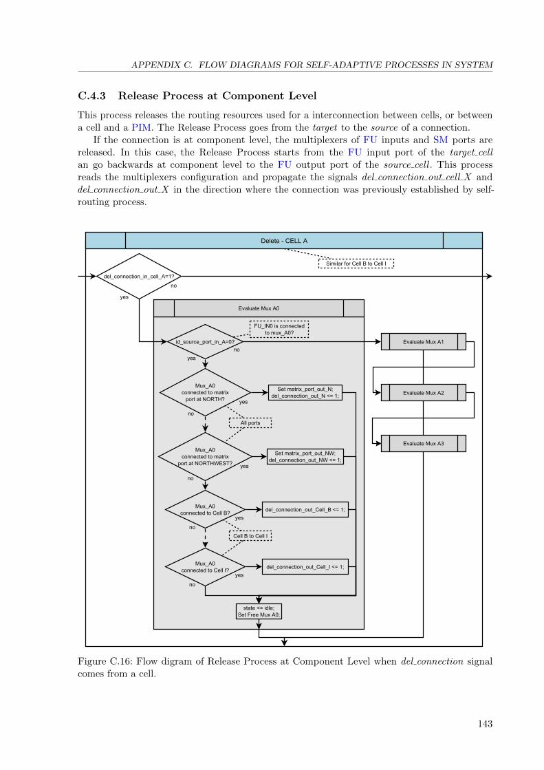
APPENDIX C. FLOW DIAGRAMS FOR SELF-ADAPTIVE PROCESSES IN SYSTEM
C.4.3 Release Process at Component Level
This process releases the routing resources used for a interconnection between cells, or betweena cell and a PIM. The Release Process goes from the target to the source of a connection.
If the connection is at component level, the multiplexers of FU inputs and SM ports arereleased. In this case, the Release Process starts from the FU input port of the target cellan go backwards at component level to the FU output port of the source cell . This processreads the multiplexers configuration and propagate the signals del connection out cell X anddel connection out X in the direction where the connection was previously established by self-routing process.
del_connection_in_cell_A=1?
yes
no
Delete020CELL0A
Similar0for0Cell0B0to0Cell0I
Mux_A0connected0to0matrix
port0at0NORTH? yes
Set0matrix_port_out_N;del_connection_out_N0<=01;
Set0matrix_port_out_NW;del_connection_out_NW0<=01;
del_connection_out_Cell_B0<=01;
state0<=0idle;Set0Free0Mux0A0;
yes
yes
Evaluate0Mux0A0
no
no
no
Mux_A0connected0to0matrix
port0at0NORTHWEST?
no
yes
id_source_port_in_A=0?
FU_IN00is0connectedto0mux_A0?
Mux_A0connected0to0Cell0B?
del_connection_out_Cell_I0<=01;
yes
no
Mux_A0connected0to0Cell0I?
All0ports
Cell0B0to0Cell0I
Evaluate0Mux0A1
Evaluate0Mux0A2
Evaluate0Mux0A3
Figure C.16: Flow digram of Release Process at Component Level when del connection signalcomes from a cell.
143

C.4. SELF-ROUTING PROCESSES IN SMCU
The target cell starts the process presented in Figure C.5 when the flag start delete cellconnection is set. Then, the target cell executes the flow diagram presented in Figure C.9.Thereafter, the SM that receives the signal del connection in cell X executes the algorithmpresented in Figure C.16.
The process continues at component level. The SMs propagate the appropriate del connectionsignal. If the source cell does not belong to the cluster, the SM propagates the signal delconnection out X and the process continues in other cluster as shown in Figure C.17.
The process continues until it reaches the source cell , which ends the process setting theglobal signal routing complete as shown in Figure C.5 in the box denoted as “Delete Matrix”.
del_connection_in_N=1?
yes
no
Similar;for;NORTHEASTD;EASTD;SOUTHEASTD;SOUTHD;SOUTHWESTD;WESTD;NORTHWEST
yes
state;<=;idle;Set;Free;Mux_SM_N0;
yes
yes
Evaluate;Mux;NORTH;0
no
no
no
no
yes
matrix_port_in_N=0?
SM;at;NORTH;isconnected;usign;port;N0?
yes
no
All;Cells
From;port;NORTHEAST;to;NORTHWEST
Evaluate;Mux;NORTH;1
Evaluate;Mux;NORTH;2
Mux_N0connected;to;matrix
port;at;NORTHEAST?
Mux_A0connected;to;matrix
port;at;NORTHWEST?
Mux_N0connected;to;Cell;A?
Mux_N0connected;to;Cell;I?
del_connection_out_Cell_A;<=;1;
Set;matrix_port_out_NE;del_connection_out_NE;<=;1;
del_connection_out_Cell_I;<=;1;
Set;matrix_port_out_NW;del_connection_out_NW;<=;1;
Delete;Matrix;NORTH
Figure C.17: Flow digram of Release Process at Component Level when del connection signalcomes from a Switch Matrix.
144

APPENDIX C. FLOW DIAGRAMS FOR SELF-ADAPTIVE PROCESSES IN SYSTEM
C.5 Conclusions
This section presents the flow diagrams of self-adaptive algorithms implemented in the Configu-ration Units of Cells and Switch Matrices.
The Cell Configuration Unit (CCU) is the start point for the execution of any process in systemthat requires the propagation of signals using the expansion ports of cells, SMs and PIMs. TheCCU includes the following algorithms:
I The self-placement algorithm is divided in two. The first is the algorithm for the insertion ofthe first cell of a component, and the second is the algorithm for the insertion of other cellsof a component (from the second).
I Since the insertion of the second cell of a component the self-routing at cell level algorithmis executed. This is implemented with the following process: first, the selection of sourceand target cells for the connections to be routed, and later the Expansion Process at CellLevel, which is divided in Search and Configuration Phases. This process is repeated for allconnections that can be routed for the new inserted cell.
I The flow diagrams for the Release Process at Cell Level are presented. These algorithmspermits to release the routing resources at cell level used for the interconnection of the FUports of two cells. These algorithms are used for self-derouting process, before eliminating asingle cell or deleting an entire component.
The Switch Matrix Configuration Unit (SMCU) includes the following algorithms:
I The Expansion Process at Component Level, which is divided in Search and ConfigurationPhases. This process is repeated for all connections that can be routed for the components.
I The flow diagrams for the Release Process at Component Level are presented. These algorithmspermit to release the routing resources at component level used for the interconnection ofthe FU ports of two cells belonging to different components. These algorithms are used forself-derouting process, before eliminating a single cell or deleting an entire component.
145

Appendix D
SANE Project Developer (SPD)
You only live once, but if you do it right,once is enough.
Solo se vive una vez, pero si lo haces bien,una vez puede ser suficiente
Mae West (1893 – 1980)
Abstract: This section describes the main features of the software tool SANE Project
Developer (SPD). It presents all functions included in the software. Additionally, it is presented
the basic syntax consideration for most common files that will be edited in SPD. The protocol
for downloading files to prototype is shown at the end of this chapter.
D.1 Description
In the design phase of the architecture, one of the the main inconveniences was the creation ofapplications that permit to test the system. This process consisted in the creation of a SANEASSEMBLY (SANE-ASM), that includes a specific number of interconnected components, andinterconnected cells inside each component. Additionally, multiple processors had to be manuallyprogrammed and compiled. Any modification in the application implies a lot of time rewritingthe data for its configuration. Similar to any commercial general purpose device a software toolis fundamental for improving the capacity of a designer when developing applications.
The SANE Project Developer (SPD) is an Integrated Development Environment (IDE)developed in C Sharp with Microsoft Visual C# 2008. The SPD permits the user –in a friendlyway– the creation and edition of projects that describe any SANE-ASM application designed. TheSPD includes an adaptation of the project ICSharpCode.TextEditor[37], which is a feature-richtext editor control that provides the SPD with a powerful tool for edition of files in a project1.The text editor for SPD includes a specific configuration for syntax highlight of files related withthe project, as well as other basic features for an advanced edition of files.
The SPD allows generating and downloading the memory initialization data for the controlmicroprocessor inside the prototype. The SPD allows the creation of files that describe theconfiguration of a SANE-ASM. This files are called SASM files, which includes the high-level (orSASM) instructions described in Chapter 5. For writing the Program Memories of the processors,
1ICSharpCode.TextEditor is licensed under The MIT License.
147

D.1. DESCRIPTION
12
53
4
6
7
Figure D.1: Screen capture of SANE Project Developer.
Assembler (ASM) files will be created, this permits to execute the functionality of a processorin the cell (between 1 and 4 per cell depending of operation mode).
The SPD supports building of the final hexadecimal file with the configuration of the SANE-ASM that will be implemented in the FPGA. This process includes the compilation of the filesinvolved in the process according to the SASM file. The SPD generates a list of errors, warningsand infos for all files involved in the building process and guides the user to make the appropriatecorrections if required. The SPD also supports the compilation of individual ASM files.
Figure D.1 shows a screen capture of the SPD, which shows the SASM file for the DynamicFault Tolerance Application presented in Section 5.5. It is also shown the structure of the solutionin the left tree and the output of the result of building process in the bottom section. Below arethe features of the main form presented in the figure by means of numeric labels:
1 Menu Strip: it includes the following menus: File, Edit, Project, Tools, View, Communica-tion, Help and Admin (only available for developer). All actions that SPD is able to executeare included in these menus, which will be detailed later in this chapter.
2 Top Tool Strip: it includes buttons for easy access to most common functions in SPD. All
148

APPENDIX D. SANE PROJECT DEVELOPER (SPD)
this functions are included in the Menu Strip.
3 Left panel: it includes a Tree View object that contains the hierarchical organization ofthe project. This tree could be shown in Cell View or Folders View. The figure shows thetree for a Cell View, which shows the project organized in components and cells. Cell Viewincludes all files associated with the project, whilst Folders View includes all files in projectfolder.
4 Buttons for Left Panel: these buttons permit the configuration the Tree View objectin Left Panel. It includes the option to alternate between Cell View and Folder View,visualization of full path of files, visualization of tooltip text and option to force a Refreshover the tree.
5 Main Tab Control: it includes the Tab Pages that could be edited by SPD. These tabsare divided in three categories:
(a) Project Tab: This tab permits to configure specific options for a project created bySPD. The configuration of components and cells in a project will be detailed later inthis chapter.
(b) Communication Tab: This tab represents the data that is sent and received fromprototype by means of serial port connections (RS-232). The SPD permits to config-ure between one and two communication panels. This tab is used for two purposes:the visualization of data downloaded to prototype using an adaptation of XMODEMprotocol, and the visualization of the execution of a SANE-ASM in the prototype fordebugging purposes (for two chips in prototype).
(c) Text Editor. The tabs that includes any file could be edited using the text editoradapted for the application. This editor includes a specific configuration for syntaxhighlight of files with the following extensions: *.ASM, *.HEX, *.INC, *.SASM and *.SHEX.
6 Output Tab Control: it includes two tab pages:
(a) Console Tab: this tab shows information of all functions that are being executed inthe SPD. This tab s mainly used for debugging purposes.
(b) Output Tab: this tab is updated each time that a ASM file is compiled or the projectis built. This tab shows Warnings, Informations, Errors and the result of the processexecuted. It permits to navigate in a friendly way to the file associated with the message,and presents the appropriate information related with the message.
7 Status Bar: This bar shows the status of some features of SPD as follows:
(a) Status and configuration of communication ports.
(b) Result of a single file compilation, or built of a project.
(c) Progress of a process that spends time, like downloading of data to the prototype andothers.
D.2 Files Edition
Table D.1 shows a description of files that SPD is able to edit. The ASM and SASM files are themost frequent files that will be edited in a project using the text editor. The SPD is not casesensitive for reserved words.
149

D.2. FILES EDITION
FileExtension
Description
*.SP SANE Assembly Project. This file is automatic configured for the SPD.It is advisable does not edit manually this file because the project might becorrupted.
*.SASM 4 SANE Assembler file. It corresponds to the high-level configuration file,which includes the SASM instructions.
*.SHEX 4 SANE Hexadecimal File. This file is generated when the project is built.The file is generated taking into account the active *.sasm file.
*.SXM SANE XMODEM File. This file is generated when the project is built.The file is generated taking into account the active *.sasm file. It is used fordownloading the project to prototype memory.
*.ASM 4 Assembler file. It corresponds to the code implemented in processors of cells.
*.INC 4 Include file. It corresponds to libraries for *.asm files.
*.HEX 4 Hexadecimal File. This file is generated when an individual *.asm file iscompiled.
*.LOG Communication LOG Files. It corresponds to the communication activitiesrelated with the RS-232 ports.
*.TXT Text Files. It corresponds to plain text for general purpose.
*.* Any Files. The SPD allows the creation of any editable file in plain text.
4 The files with this extension includes syntax highlight.
Table D.1: Relation of files for SANE Project Developer.
D.2.1 Assembler Files
The Assembler (ASM) files correspond to the code implemented in the processors of cells. De-pending on configuration mode, it is possible to have between one to four ASM files per cell. TheSPD includes the following features for ASM files:
I Reserved words for instructions:
ADDLW , SUBLW , ANDLW , IORLW , XORLW , MOVLF , ADDWY , SUBWY ,
ANDWY , IORWY , XORWY , MOVW , BLMOV , COMW , NEGW , INCW , DECW ,
SWAPW , RLW , RRW , LSL , LSR , ASL , ASR , CLRF , CLC , SEC , END ,
NOP , BCLR , BSET , BRCLR , BRSET , GOTO , BZ , BNZ , BC , BNC ,
CBEQ , CBGE , CBGT , CBNE , DBNZ , IBNZ.
I Reserved words for directives:
EQU , ORG , MODE_CORE , #INCLUDE
I Numbers format:
• Hexadecimal (default): 0xe9, 0XE9, e9, h’E9’, H’e9’
• Decimal: d’233’, D’233’, .233
• Octal: o’351’, O’351’
• Binary: b’11101001’, B’11101001’
150

APPENDIX D. SANE PROJECT DEVELOPER (SPD)
• ASCII: a’G’, A’k’ (one alphanumeric character, from ASCII 20h to 7Eh).
I Comments and labels: The labels must start with a letter or underscore (a-z,A-Z,_),later may include any other alphanumeric character. The comments can be included with anysequence of text after semicolon or double-slash:
label1 ;This is a label
movlf .255,bin8 ,0 ;Example 1 of a comment
cycle_38 //This is another label
BLMOV BL_IN0 ,0x3F // Example 2 of a comment
D.2.2 SANE Assembler Files
The SANE Assembler (SASM) files corresponds to the high-level configuration file for theimplementation of a SANE-ASM in the system. The SPD includes the following features forSASM files:
I Reserved words for instructions:
CREATE_COMPONENT , CONNECT_COMPONENT , DELETE_COMPONENT ,
WRITE_FU_MEMORY , WRITE_FU_MEMORY_CR , WRITE_FU_MEMORY_PM0 ,
WRITE_FU_MEMORY_PM1 , WRITE_FU_MEMORY_PM2 ,
WRITE_FU_MEMORY_PM3 , RESTART_PROCESSORS ,
DISABLE_PROCESSORS , RESTART_AND_DISABLE_PROCESSORS ,
ENABLE_PROCESSORS , WAIT , RESTART_PROCESSORS_WAIT ,
ENABLE_PROCESSORS_WAIT , END , START_SUBPROCESS_0 ,
END_SUBPROCESS_0 , START_SUBPROCESS_1 , END_SUBPROCESS_1 ,
START_SUBPROCESS_2 , END_SUBPROCESS_2 , START_SUBPROCESS_3 ,
END_SUBPROCESS_3 , FT_CONFIGURATION.
I Reserved words for directives:
EQU
I Numbers format:
• Hexadecimal (default): 0xe9, 0XE9, e9, h’E9’, H’e9’
• Decimal: d’233’, D’233’, .233
• Octal: o’351’, O’351’
• Binary: b’11101001’, B’11101001’
• ASCII: a’G’, A’k’ (one alphanumeric character, form ASCII 20h to 7Eh).
I Comments: The comments can be included with any sequence of text after semicolon ordouble-slash:
primary_cell equ 0xAAAA0001 ;cell definition - hexa
redundant_cell equ d’8613’ //cell definition - decimal
comp_A equ 0xAAAA // component definition hexa
ft_configuration primary_cell ,redundant_cell ;Comment style 1
create_component comp_A // Comment style 2
151

D.3. FUNCTIONS
D.3 Functions
The SPD includes all necessary tools for developing and executing applications in the prototype.Any SANE-ASM application is implemented by means of a Project, which includes all files relatedwith the application. The main characteristics of the SPD are included in the Main Menu, whichpermits the user to execute the corresponding action as shown bellow. In many cases the nameof the option selected denotes the action that will be executed and does not require additionalexplanation.
D.3.1 File Menu
It includes tools for management of projects and files. The options included in this menu arepresented bellow:
1. New Project. Starts a template for creation of a new project.2. Open Project.3. Close Project.4. Save Project As...5. Save File As...6. Save ‘*.*’. Save current file or tab selected in Main Panel (Ctlr+S).7. Save All. Save all files (Ctlr+Shift+S).8. Close ‘*.*’. Close current file or tab selected in Main Panel.9. Close all except selected tab. Close all files except the selected tab in Main Panel.
10. New File. Start a template wizard for creation of a new file. The new file could be createdwith a basic configuration template for files *.asm, *.sasm and *.txt.
11. Open File.12. Rename File.13. Delete File.14. Recent Projects. List of recent projects for quick access.15. Recent Files. List of recent files for quick access.16. Exit.
D.3.2 Edit Menu
This menu includes basic and advanced tools for edition of files. The options included in thismenu are presented bellow:
1. Split text area. This options permits visualization of a file in two different segments of code.2. Cut (Ctlr+X).3. Copy (Ctlr+C).4. Paste (Ctlr+V).5. Delete.6. Select All (Ctrl+A).7. Find ... (Ctrl+F).8. Find and replace ... (Ctrl+H).9. Find again (F3).
10. Find again reverse (May+F3)11. Display. This is a sub-menu that permits the following actions over text editor:
I Show line numbers.I Show end of line markers.I Highlight current line.
152

APPENDIX D. SANE PROJECT DEVELOPER (SPD)
I Show spaces and tabs.I Highlight matching brackets when cursor is after.I Allow cursor past end of line.
12. Bookmark. This is a sub-menu that permits the following action over text editor:I Toogle bookmark. (Ctrl+F2).I Goto next bookmark. (F2).I Go to previous bookmark. (May+F2).I Clear all bookmark.
13. Uppercase/Lowercase. This is a sub-menu that permits the following actions over texteditor:I Convert to uppercase. (Ctrl+Shift+U).I Convert to lowercase. (Ctrl+U).
14. Advanced. This is a sub-menu that permits the following actions over text editor:I Toggle line comments. (Alt+Q).I Convert spaces to tabs.I Convert tabs to spaces.
D.3.3 Project Menu
This menu includes tools for the current project opened as follows:
1. Component Editor (F5). Tool that permits to edit the components configuration in project.Figure D.2 shows the tool implemented fo this purpose. Note that there are two differentviews, one for addition and the other for edition. This tool permits the user configure thecomponents and cells for a specific project.
2. Cell Editor (F6). Tool that permits to edit the cells configuration in project. Figure D.3shows the tool implemented for this purpose. This tool permits the user to configure the cellspreviously included in the project. Thus, the user is able to edit the Configuration Registers,Connection Tables and the ASM files associated to each CORE.
3. SASM Configuration Files (F7). Tool that permits to add and select the SASM files toproject. Figure D.4 shows the tool implemented for this purpose. This tool permits to addand/or activate the SASM file that will be used when “Built Project” tool is executed. Notethat SPD permits to have many different SASM files, but only one can be activated.
4. Compile File (F9). Compile the selected ASM file. This tool generates a *.HEX file withthe same name of the correspondent *.ASM file. This function could be executed previouslyto built the project for detecting error or warnings in ASM files. In this case, the softwareguides the user to find the source of the correspondent message.
5. Built Project (F10). Bulit the project taking into account the active SASM file. This toolgenerate the files *.SASM and *.SXM with the same name of the active *.SASM file. This is thelast function that must be executed before downloading the configuration file (SXM) to CµPmemory in prototype. If there are errors or warnings in this process, the software guides theuser to find the source of the correspondent message.
6. Add copy of source. This tool permits to make a copy of any file to the project folder.
153

D.3. FUNCTIONS
(a) Add mode.
(b) Edit mode.
Figure D.2: Component editor tool.
D.3.4 Tool Menu
This menu includes the following options:
1. Export. This is a sub-menu that permits the user perform the following actions:
I Figure. Exports a figure that represents the architecture implemented in the prototype.I Screen Capture. Exports a screen capture of the current view of SPD (formats *.png,
*.jpg, *.gif or *.bmp).I Console. Exports the console as a *.txt file.
2. Clear Console.
3. Options. This is a form that permits the user to configure several option for SPD. This formincludes five tabs as follows:
(a) General: configuration of general options for SPD.(b) Text Editor: configuration of text editor.(c) Compiler: configuration for compilation tools.(d) Tree: configuration of project visualization tree in Left Panel.(e) Communications: configuration of serial ports (RS-232) connected with prototype.(f) Figure: configuration of figure that represents the system architecture.
154

APPENDIX D. SANE PROJECT DEVELOPER (SPD)
Figure D.3: Cell editor tool.
Figure D.4: Tool for addition/activation of SANE assembler files.
155

D.3. FUNCTIONS
D.3.5 View Menu
This menu is used for accessing some special Page Tabs object. Note that project and commu-nication tabs could be closed in the same way of a text editor tab. It includes the followingoptions:
1. Project Tab. Permits to open the project tab for edition of components, cells and addi-tion/activation of SASM files.
2. Communication Tab. Permits to open the communication tab for visualization of processesexecuted in serial ports.
3. Console Tab. Permits to open the console tab for debugging purposes.
D.3.6 Communication Menu
This menu includes the tools related with the serial port communication, which are used tosend/receive information to FPGAs in prototype. Some of the functions listed bellow are detailedin section D.4. This menu includes the following options:
1. Open/close Communication Ports. This tool opens or closes the serial ports configuredfor communication with FPGAs in prototype. Additionally, this tool starts or stops threadsthat permits the correct management and visualization of data in communication panels.
2. Clear Communication Panles.
3. Save copy of communication logs.
4. Communication Test. Execute a communication test between the SPD and the CµP inthe prototype. It permits to check the correct configuration of serial ports for the executionof other functions over CµP memory.
5. Clear Memory. Execute a process to clear all section of memory in CµP dedicated for theSASM configuration file.
6. Write Memory. Execute a process to write the SXM file that was previously generatedwith the “Built Project” function. This file is written in section of memory dedicated for thehigh-level configuration file.
7. Read Memory. Execute a process to read the entire section of memory dedicated for thehigh-level configuration file.
8. Cancel FPGA communication process. This function permits to cancel in a safe wayany process that has been started for a communication between the SPD and the CµP.
D.3.7 Help and Admin Menus
The Help menu presents the credits of the SPD (About). Note that this chapter can be used asa User Manual for the software implemented. The Admin menu is only available for debuggingor developer options. It is activated executing the SPD with the argument: /admin.
156

APPENDIX D. SANE PROJECT DEVELOPER (SPD)
Field Name Description
<CB> Control Byte Define the process that will be executed:<CB> = 0x01: Communication test.<CB> = 0x02: Clear Memory.<CB> = 0x03: Write Memory.<CB> = 0x04: Read Memory.
<DB> Data Bytes Denote the zero-based number of bytes send or received inthe frame (0x00 to 0xFF represents 1 to 256 bytes)
<AAA1> Address 1 Initial address for write/read operations (2 bytes).
<AAA2> Address 2 Final address for read operations (2 bytes).
<D0 D1···D255> Data Bytes Bytes sent or received in frame. The amount of data bytesdepends on the Data Bytes field.
<CKS> Checksum Two’s complement of the arithmetic sum of the bytes inframe except the <SOH> and <CRC>. Final carry is discarded.
Table D.2: Description of fields for XMODEM based protocol.
D.4 Downloading Project to Prototype
The SPD and the CµP implements an adaptation of the XMODEM protocol for downloadingprojects to prototype. XMODEM, like most file transfer protocols, breaks up the original data intoa series of “packet” or “frames“ that are sent to the receiver, along with additional informationallowing the receiver to determine whether that packet was correctly received. Xmodem is a half-duplex communication protocol. The following bytes are defined for the protocol implemented:
I <SOH> = 0x01: Start of Heading.I <EOT> = 0x04: End of Transmission.I <ACK> = 0x06: Acknowledge.I <NACK>= 0x15: Negative Acknowledge.I <CAN> = 0x18: Cancel.
The frames sent or received have the structure presented below. Note that additional fieldsare only used when the frame starts with the byte <SOH>. The description of additional fields isshown in Table D.2.
<SOH> [<CB>] [<DB>] [<AAA1>] [<AAA2>] [<D0 D1 ... D255>] <CKS>
There are four basic functions implemented in SPD, which corresponds to the four values ofthe field “Control Byte”. These functions are described in Sections D.4.1 to D.4.4. Note that thereceiver, after receiving a packet, will either acknowledge (ACK) or not acknowledge (NACK) thepacket. If a NACK is received five times, the sender cancel the process sending the correspondentbyte (CAN). These sections present data flow examples including error recovery, which in normalconditions is not present in frames. The normal data flow is interrupted when an unexpectedevent is produced as follows:
1. A <NACK> is sent when there is a checksum error. On any <NACK>, the sender will re-transmitthe last packet.
2. A <CAN< is sent when there is a format error or five <NACK> has been received.
3. When a <CAN> is received, the process is finalized and no more bytes are sent.
157

D.4. DOWNLOADING PROJECT TO PROTOTYPE
D.4.1 Communication Test
This function permits the user to ensure that communication with the prototype is configuredproperly. Table D.3 shows the data flow executed for communication test (<CB>=0x01).
SANE Project Developer ↔ Prototype
<SOH><01><CKS> →← <NACK>1
<SOH><01><CKS> →← <ACK>
<EOT> →← <ACK>
1 Framing error on any byte.
Table D.3: Example of data flow for Communication Test with prototype.
D.4.2 Clear Memory
This function permits to clear the entire section of memory dedicated to the configuration file inthe prototype. Table D.4 shows the data flow executed for clear memory (<CB>=0x02).
SANE Project Developer ↔ Prototype
<SOH><02><CKS> →← <NACK>1
<SOH><02><CKS> →← <ACK>
<EOT> →← <ACK>
1 Framing error on any byte.
Table D.4: Example of data flow for Clear Memory in prototype.
D.4.3 Write Memory
This function permits to write a portion of the memory in prototype, which corresponds to thehigh-level configuration file (SASM file). The format of the first frame sent by SPD is shownbellow:
<SOH> <CB=0x03> <DB> <AAA1> <D0 D1 ... D255> <CKS>
Table D.5 shows an example of the data flow executed for write five 32-bit words in memory,i.e., from address 0x0000 to 0x0004 (<CB>=0x03).
Note that words in prototype memory are 32-bit width. Therefore, the Data Bytes must be amultiple of 4 in zero-based range, e.g., 0x03, 0x07, 0x0B. This implies that address is incrementedeach four data bytes as shown in the example. If the SPD receives NACK five times, the SPDsends the byte <CAN> and the process ends.
158
APPENDIX D. SANE PROJECT DEVELOPER (SPD)
SANE Project Developer ↔ Prototype
<SOH><03><07><0000><00 01 02 03 04 05 06 07><CKS> →← <ACK>
<SOH><03><07><0002><08 09 0A 0B 0C 0D 0E 0F><CKS> →← <NACK>1
<SOH><03><07><0002><08 09 0A 0B 0C 0D 0E 0F><CKS> →← <ACK>
<SOH><03><03><0004><10 11 12 13><CKS> →← <ACK>
<EOT> →← <ACK>
1 Framing error on any byte.
Table D.5: Example of data flow for Write Memory in prototype.
D.4.4 Read Memory
This function permits to read a portion of the memory in prototype, which corresponds to thehigh-level configuration file (SASM file). The format of the first frame sent by SPD is shownbellow:
<SOH> <CB=0x04> <DB> <AAA1> <AAA2> <CKS>
The format of the frame with data bytes sent by CµP is shown bellow:
<SOH> <DB> <AAA1> <D0 D1 ... D255> <CKS>
Table D.6 shows an example of the data flow executed for read five 32-bit words in memory,i.e., form address 0x0000 to 0x0004 (<CB>=0x04).
Note that words in prototype memory are 32-bit width. Therefore, the Data Bytes must be amultiple of 4 in zero-based range, e.g., 0x03, 0x07, 0x0B. This implies that address is incrementedeach four data bytes as shown in the example. If the SPD receives NACK five times, the SPDsends the byte <CAN> and the process ends.
The size of the data sent by CµP depends on the Data Bytes argument received the firsttime. Only the last Data Bytes field is modified by CµP, when the number of bytes does notcorrespond with the remaining bytes that will be sent.
159
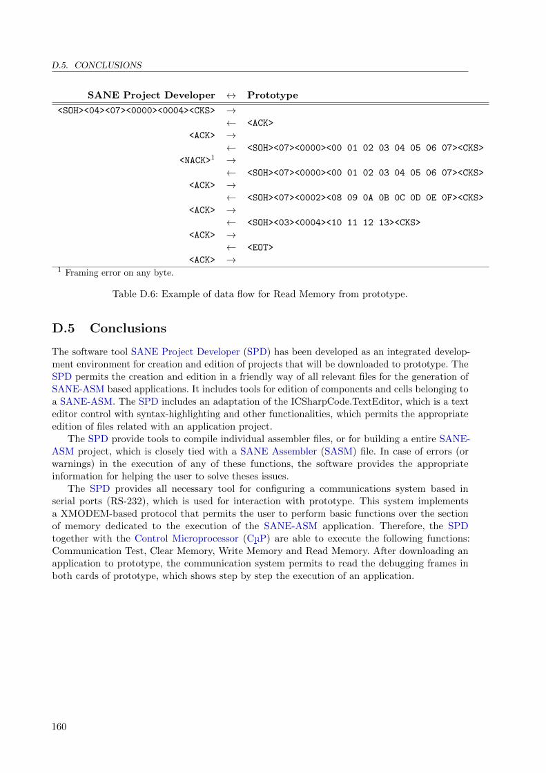
D.5. CONCLUSIONS
SANE Project Developer ↔ Prototype
<SOH><04><07><0000><0004><CKS> →← <ACK>
<ACK> →← <SOH><07><0000><00 01 02 03 04 05 06 07><CKS>
<NACK>1 →← <SOH><07><0000><00 01 02 03 04 05 06 07><CKS>
<ACK> →← <SOH><07><0002><08 09 0A 0B 0C 0D 0E 0F><CKS>
<ACK> →← <SOH><03><0004><10 11 12 13><CKS>
<ACK> →← <EOT>
<ACK> →1 Framing error on any byte.
Table D.6: Example of data flow for Read Memory from prototype.
D.5 Conclusions
The software tool SANE Project Developer (SPD) has been developed as an integrated develop-ment environment for creation and edition of projects that will be downloaded to prototype. TheSPD permits the creation and edition in a friendly way of all relevant files for the generation ofSANE-ASM based applications. It includes tools for edition of components and cells belonging toa SANE-ASM. The SPD includes an adaptation of the ICSharpCode.TextEditor, which is a texteditor control with syntax-highlighting and other functionalities, which permits the appropriateedition of files related with an application project.
The SPD provide tools to compile individual assembler files, or for building a entire SANE-ASM project, which is closely tied with a SANE Assembler (SASM) file. In case of errors (orwarnings) in the execution of any of these functions, the software provides the appropriateinformation for helping the user to solve theses issues.
The SPD provides all necessary tool for configuring a communications system based inserial ports (RS-232), which is used for interaction with prototype. This system implementsa XMODEM-based protocol that permits the user to perform basic functions over the sectionof memory dedicated to the execution of the SANE-ASM application. Therefore, the SPDtogether with the Control Microprocessor (CµP) are able to execute the following functions:Communication Test, Clear Memory, Write Memory and Read Memory. After downloading anapplication to prototype, the communication system permits to read the debugging frames inboth cards of prototype, which shows step by step the execution of an application.
160

Appendix E
Listings of Example Applications
Just as iron rusts from disuse,even so does inaction spoil the intellect.
Ası como el hierro se oxida por falta de uso,tambien la inactividad destruye el intelecto.
Leonardo Da Vinci (1452 – 1519)
Abstract: This chapter presents a set of listings related with application examples devel-
oped for testing the self-adaptive hardware architecture described in this document. These
listings include *.SASM and *.ASM files, which represents the high-level configuration file for
the configuration of an application, and the threads scheduled for processors in cells.
The listings shown in this chapter are related with two projects with example applications:
I The first is a Dynamic Fault Tolerance Scaling application, which demonstrates the correctexecution of runtime self-configuration by means of subprocesses (Section 5.5).
I The second is related with the Static Fault Tolerance mechanism, which demonstrates theself-repair ability of the system by means of self-elimination and self-replications of damagedcells when a hardware failure is detected (Section 5.6).
Tables E.1 and E.2 show a relation of listings presented in this section. Each listing isexplained by means comments in code, therefore no additional explanation will be added alongthis chapter.
161

References Listing Description
Application descriptionin Section 5.5.
Listings in Section E.1
E.1 SASM file with high-level configuration of application.
E.2 ASM file with code for Monitor 1 Section.
E.3 ASM file with code for Monitor 2 Section.
E.4 ASM file with code for original copy of Compute Section(copy0). The code for first copy (copy1) and second copy(copy2) of Compute Section is the same.
E.5 SHEX file generated after building project. This listingshows the instructions code implemented in section ofmemory of CµP dedicated to SANE-ASM configuration.
E.6 SXM file generated after building project. For visualiza-tion purposes, the SXM file was generated with eight32-bit word per line. However, the SPD could be config-ured to write between 1 to 32 words per line (defaultvalue is 16).
Table E.1: Listings for Dynamic Fault Tolerance Scaling application example.
References Listing Description
Application descriptionin Section 5.6.
Listings in Section E.2
E.7 SASM file with high-level configuration of application.
E.8 ASM file with code for Working Processor in Primarycell. The code for Redundant Processor in RedunadntCell is the same. A modification in the sequence must beperformed manually in one of this files to test the StaticFault Tolerance mechanism as shown in listing.
E.9 ASM file with delay function for visualization of sequencein leds.
E.10 SHEX file generated after building project. This listingshows the instructions code implemented in section ofmemory of CµP dedicated to SANE-ASM configuration.
E.11 SXM file generated after building project. For visualiza-tion purposes, the SXM file was generated with eight32-bit word per line. However, the SPD could be config-ured to write between 1 to 32 words per line (defaultvalue is 16).
Table E.2: Listings for Static Fault Tolerance application example.
162

APPENDIX E. LISTINGS OF EXAMPLE APPLICATIONS
E.1 Listings for Dynamic Fault Tolerance Scaling ApplicationExample
Listing E.1: SASM file for configuration of Dynamic Fault Tolerance Scaling application.
1 ; ----------------------------------------------------------------------------------
2 ;-- SANE assembly file template for Project DFT_APP_TESIS
3 ;-- Created by: SANE Project Developer - v 2.20 - Javier Soto Vargas
4 ;-- Engineer: JSV
5 ;--
6 ;-- Create Date: 22/02/2013 17:12:19
7 ;-- Project Name: DFT_APP_TESIS
8 ;-- Filename: ConfFile_1 .3. sasm
9 ;-- Description : SASM file for Dynamic Fault Tolerace example application .
10 ;--
11 ;-- Revision 0.01 - File created.
12 ;-- Additional Comments:
13 ;--
14 ; ----------------------------------------------------------------------------------
15 ; ************************************
16 ;Final configuration after execution
17 ; ************************************
18 ;CHIP0 |-----| |-----| CHIP1 |-----| |-----|
19 ; | C00 | | C10 | | C00 | | C10 |
20 ; |-----| |-----| |-----| |-----|
21 ;
22 ; |-----| |-----| |-----| |-----|
23 ; | C01 | | C11 | | C01 | | C11 |
24 ; |-----| |-----| |-----| |-----|
25
26 ; c00_CHIP0: address =0 x00CC00C0 , MODE =0x09 , PORTS =0x44 , FTCSR =0 x00.
27 ; Pseudo -random number generator (PRNG) using a linear
28 ; feedback shift register (LFSR). Compute Section (PRNG_0).
29 ; c01_CHIP0: address =0 x11AA00A1 , MODE =0x09 , PORTS =0x44 , FTCSR =0 x00.
30 ; Monitor_1 : monitor.
31 ; c10_CHIP0: address =0 x11AA00A2 , MODE =0x04 , PORTS =0x00 , FTCSR =0 x00.
32 ; Monitor_2 : comparator .
33 ; c11_CHIP0: address =0 x11CC00C1 , MODE =0x09 , PORTS =0x44 , FTCSR =0 x00.
34 ; First copy of Compute section (PRNG_1).
35 ; This component (1 cell) is dinamically created and deleted.
36 ; c00_CHIP1: address =0 x22CC00C2 , MODE =0x09 , PORTS =0x44 , FTCSR =0 x00.
37 ; Second copy of Compute section (PRNG_2).
38 ; This component (1 cell) is dinamically created and deleted.
39 ;others : empty.
40
41 ; **********************************
42 ; Difinitions
43 ; **********************************
44 comp_compute equ 0x00CC
45 comp_compute_copy_1 equ 0x11CC
46 comp_compute_copy_2 equ 0x22CC
47 comp_monitor equ 0x11AA
48 cell_lfsr equ 0x00CC00C0
49 cell_lfsr_copy_1 equ 0x11CC00C1
50 cell_lfsr_copy_2 equ 0x22CC00C2
51 cell_monitor_1 equ 0x11AA00A1
52 cell_monitor_2 equ 0x11AA00A2
53 ; **********************************
54 ; subprocess 0 for Monitor component
55 ; **********************************
56 start_subprocess_0 comp_monitor
57 create_component comp_compute_copy_1 ;Create Compute section , copy 1
58 write_FU_memory cell_lfsr_copy_1 ;Write FU memories for cell
59 connect_component ;connect component
60 end_subprocess_0
61 ; **********************************
62 ; subprocess 1 for Monitor component
63 ; **********************************
163

E.1. LISTINGS FOR DYNAMIC FAULT TOLERANCE SCALING APPLICATION EXAMPLE
64 start_subprocess_1 comp_monitor
65 create_component comp_compute_copy_2 ;Create Compute section , copy 2
66 write_FU_memory cell_lfsr_copy_2 ;Write FU memories for cell
67 connect_component ;connect component
68 end_subprocess_1
69 ; **********************************
70 ; subprocess 2 for Monitor component
71 ; **********************************
72 start_subprocess_2 comp_monitor
73 delete_component comp_compute_copy_1 ;delete copy 1 of Compute section
74 end_subprocess_2
75 ; **********************************
76 ; subprocess 3 for Monitor component
77 ; **********************************
78 start_subprocess_3 comp_monitor
79 delete_component comp_compute_copy_2 ;delete copy 2 of Compute section
80 end_subprocess_3
81
82 ; ************************
83 ;* Initial Configurtion *
84 ; ************************
85 create_component comp_monitor ;Create Monitor component
86 restart_and_disable_processors
87 write_FU_memory cell_monitor_1 ;write FU program memories for Monitor_1
88 write_FU_memory cell_monitor_2 ;write FU program memories for Monitor_2
89 create_component comp_compute ;Create Compute component
90 write_FU_memory cell_lfsr ;Write FU program memories for cell
91 connect_component ;Connect component
92 enable_processors_wait ;Enable processors and wait for
93 ;an event to start a subprocess .
94 end ;End of SASM configuration file
Listing E.2: ASM code for Monitor 1 section.
1 ; --------------------------------------------------------------------------
2 ;-- Assembler template for Processor Core 0 in Mode 9
3 ;-- Created by: SANE Project Developer - v 2.20 - Javier Soto Vargas
4 ;-- Engineer: Javier Soto
5 ;--
6 ;-- Date Created: 22/02/2013 17:12:03
7 ;-- Project Name: DFT_APP_TESIS
8 ;-- Filename: Monitor_1 .asm
9 ;-- Description : One 16-bit processor (P0) with 16 x16 data memory and 256
10 ;-- instructions . Monitor_1 section , measure the power
11 ;-- consumpsion of PRNGs , and start the creation/killing of
12 ;-- copies of compute sections.
13 ;-- Revision 0.01 - File created.
14 ;-- Additional Comments: Cell address: 0 x11AA00A1. MODE = 0x09
15 ; --------------------------------------------------------------------------
16 #include <pMode9Core0.inc > ; Definition of Configuration and Status
17 ;Registers including inputs and outputs.
18 ;16-bit General purpose Registers
19 ; Definitions for meassuring the compute section.
20 new_data equ 0x0
21 old_data equ 0x1
22 threshold equ 0x2
23 average equ 0x3
24 m1_status equ 0x4
25 cont_changes equ 0x5
26 comparison equ 0x6
27 ;FIFO for average of last eigth values
28 FIFO_0 equ 0x8
29 FIFO_1 equ 0x9
30 FIFO_2 equ 0xA
31 FIFO_3 equ 0xB
32 FIFO_4 equ 0xC
33 FIFO_5 equ 0xD
34 FIFO_6 equ 0xE
35 FIFO_7 equ 0xF
36 ; **************************************************************
164

APPENDIX E. LISTINGS OF EXAMPLE APPLICATIONS
37 ;* Description of register with status of MONITOR_1: m1_status
38 ; **************************************************************
39 ;m1_status <0> : 1 -> first copy active , 0-> no active
40 ;m1_status <1> : 1 -> second copy active , 0-> no active
41 ;m1_status <2> : 1 -> creation first copy in progress , 0-> no started
42 ;m1_status <3> : 1 -> creation second copy in progress , 0-> no started
43 ;m1_status <4> : 1 -> killing first copy in progress , 0-> no started
44 ;m1_status <5> : 1 -> killing seconf copy in progress , 0-> no started
45 ; ************************************
46 ; Description of register: comparison
47 ; ************************************
48 ;comparison <0> : 1 -> PRNG_copy_0_original == PRNG_copy1
49 ; 0 -> PRNG_copy_0_original /= PRNG_copy1
50 ;comparison <1> : 1 -> PRNG_copy_1 == PRNG_copy2
51 ; 0 -> PRNG_copy_1 /= PRNG_copy2
52 ; ************************************
53 ; Directives
54 ; ************************************
55 MODE_CORE 0x9 ,0 ;Directive for MODE and CORE
56 ORG 0x0 ;Origin of first instruction
57 ; ************************************
58 ;Start of program - initialization
59 ; ************************************
60 start
61 MOVLF 0x05 ,old_data ,1 ;Seed for LFSR 0x05F3
62 MOVLF 0xF3 ,old_data ,0
63 MOVLF 0x00 ,FIFO_0 ,1 ;Set FIFO registers to 0x000F
64 MOVLF 0x0F ,FIFO_0 ,0 ;initial value for high consumption regime ,
65 MOVW FIFO_0 ,FIFO_1 ;there are not COMPUTE sections copies
66 MOVW FIFO_0 ,FIFO_2
67 MOVW FIFO_0 ,FIFO_3
68 MOVW FIFO_0 ,FIFO_4
69 MOVW FIFO_0 ,FIFO_5
70 MOVW FIFO_0 ,FIFO_6
71 MOVW FIFO_0 ,FIFO_7
72 CLRF threshold ;Set threshold to 0x0000
73 CLRF m1_status ;Set m1_status to 0x0000
74 cycle
75 MOVW old_data ,OUT_01 ;Move old_data to OUT_01 Port two times
76 MOVW old_data ,OUT_01 ;for metaestability issues with two chips.
77 BLMOV IN_01 ,new_data ;Wait pseudo -random data from COMPUTE section
78 BLMOV IN_23 ,comparison ;Wait comparison value from MONITOR_2 section
79 GOTO calculate_average ; Calculate average
80 ret_calc_average
81 MOVW new_data ,old_data ;old_data <= new_data
82 MOVW average ,OUT_23 ;Move average to OUT_23 Port - average in leds
83 review_progress
84 BRCLR m1_status ,2,next1 ;next1 if creation copy_1 is not in progess
85 BRCLR SUBPCSR ,3,nextLast ;nextLast if ends creation of copy_1
86 ;(nextlast if ends execution of subprocess0 )
87 BCLR m1_status ,2 ;clear flag creation_first_copy_in_progess
88 BCLR SUBPCSR ,3 ;clear subprocess0 ends flag
89 BSET m1_status ,0 ;set flag copy_1 of COMPUTE section active
90 GOTO nextLast
91 next1
92 BRCLR m1_status ,3,nextLast ;nextLast if create copy_2 is not in progess
93 BRCLR SUBPCSR ,4,nextLast ;nextLast if ends creation of copy_2
94 ;(nextlast if ends execution of subprocess1 )
95 BCLR m1_status ,3 ;clear flag creation_second_copy_in_progess
96 BCLR SUBPCSR ,4 ;clear subprocess1 ends flag
97 BSET m1_status ,1 ;set flag copy_2 of COMPUTE section active
98 GOTO nextLast
99 next2
100 BRCLR m1_status ,4,next3 ;next3 if killing copy_1 is not in progess
101 BRCLR SUBPCSR ,5,nextLast ;nextLast if ends killing of copy_1
102 ;(nextlast if ends execution of subprocess2 )
103 BCLR m1_status ,4 ;clear flag kill_first_copy_in_progess
104 BCLR SUBPCSR ,5 ;clear subprocess2 ends flag
105 GOTO nextLast
106 next3
165

E.1. LISTINGS FOR DYNAMIC FAULT TOLERANCE SCALING APPLICATION EXAMPLE
107 BRCLR m1_status ,5,nextLast ;nextLast if killing copy_2 is not in progess
108 BRCLR SUBPCSR ,6,nextLast ;nextLast if ends killing of copy_2
109 ;(nextlast if ends execution of subprocess3 )
110 BCLR m1_status ,5 ;clear flag kill_second_copy_in_progess
111 BCLR SUBPCSR ,6 ;clear subprocess3 ends flag
112 nextLast
113 BRSET m1_status ,1, second_copy_active ;process when copy_2 is active
114 BRSET m1_status ,0, first_copy_active ;process when copy_1 is active
115 none_copy_active ;process when none copy is active
116 MOVLF 0x0B ,threshold ,0 ;for high consumption regime
117 CBGE average ,threshold ,cycle ;goto cycle if average >= 11
118 MOVLF 0x01 ,threshold ,0 ;for low consumption regime (copy_1)
119 CBGE average ,threshold ,pre_create_first_copy ;jump if average >= 1
120 MOVLF 0xF1 ,OUT_23 ,1 ;set error code 1 (leds)
121 END ;End with error
122 pre_create_first_copy
123 BRCLR SUBPCSR ,7,cycle ;goto cycle if system is not in wait state
124 create_first_copy
125 BSET m1_status ,2 ;set flag creation_first_copy_in_progress
126 BCLR SUBPCSR ,2 ;configure creation of first copy
127 BCLR SUBPCSR ,1 ;subprocess0 , SUBPCSR <2:1 > <= 00
128 BSET SUBPCSR ,0 ;start creation of first copy
129 BCLR SUBPCSR ,0 ;(start execution of subprocess_0 )
130 GOTO cycle
131
132 org 0x40 ;Optional , for locating code in PM1
133 ; ************************************
134 ;Process when first copy is active
135 ; ************************************
136 first_copy_active
137 BRSET comparison ,0,$+3 ;jump 3 positions if copy_original == copy_1
138 MOVLF 0xF2 ,OUT_23 ,1 ;set error code 2 (leds)
139 END ;End with error
140 MOVLF 0x0B ,threshold ,0 ;for high consumption regime
141 CBGE average ,threshold ,pre_delete_first_copy ;jump if average >= 11
142 MOVLF 0x06 ,threshold ,0 ;for medium consumption regime
143 CBGE average ,threshold ,cycle ;jump if average >= 6
144 MOVLF 0x01 ,threshold ,0 ;for low consumption regime
145 CBGE average ,threshold ,pre_create_second_copy ;jump if average >= 1
146 MOVLF 0xF3 ,OUT_23 ,1 ;set error code 3 (leds)
147 END ;End with error
148 pre_delete_first_copy
149 BRCLR SUBPCSR ,7,cycle ;goto cycle if system is not in wait state
150 delete_first_copy
151 BCLR m1_status ,0 ;clear flag first_copy_active
152 BSET m1_status ,4 ;set flag kill_first_copy_in_progress
153 BSET SUBPCSR ,2 ;configure subprocess for killing first copy
154 BCLR SUBPCSR ,1 ;subprocess2 , SUBPCSR <2:1 > <= 10
155 BSET SUBPCSR ,0 ;start killing of copy_1
156 BCLR SUBPCSR ,0 ;(start execution of subprocess_2 )
157 GOTO cycle
158 pre_create_second_copy
159 BRCLR SUBPCSR ,7,cycle ;goto cycle if system is not in wait state
160 create_second_copy
161 BSET m1_status ,3 ;set flag creation_second_copy_in_progress
162 BCLR SUBPCSR ,2 ;configure subprocess for create second copy
163 BSET SUBPCSR ,1 ;subprocess_1 , SUBPCSR <2:1 > <= 01
164 BSET SUBPCSR ,0 ;start creation of copy_2
165 BCLR SUBPCSR ,0 ;(start execution of subprocess_1 )
166 GOTO cycle
167 ; ************************************
168 ;Process when second copy is active
169 ; ************************************
170 second_copy_active
171 BRSET comparison ,1,$+3 ;jump 3 positions if copy_1 == copy_2
172 MOVLF 0xF4 ,OUT_23 ,1 ;set error code 4 (leds)
173 END ;End with error
174 MOVLF 0x06 ,threshold ,0 ;for medium consumption regime
175 CBGE average ,threshold ,pre_delete_second_copy ;jump if average >= 6
176 MOVLF 0x01 ,threshold ,0 ;for low consumption regime
166

APPENDIX E. LISTINGS OF EXAMPLE APPLICATIONS
177 CBGE average ,threshold ,cycle ;jump if average >= 1
178 MOVLF 0xF5 ,OUT_23 ,1 ;set error code 5 (leds)
179 END ;End with error
180 pre_delete_second_copy
181 BRCLR SUBPCSR ,7,cycle ;goto cycle if system is not in wait state
182 delete_second_copy
183 BCLR m1_status ,1 ;clear flag second_copy_active
184 BSET m1_status ,5 ;set flag kill_second_copy_in_progress
185 BSET SUBPCSR ,2 ; configure subprocess for killing second copy
186 BSET SUBPCSR ,1 ;subprocess_3 , SUBPCSR <2:1 > <= 11
187 BSET SUBPCSR ,0 ;start killing of copy_2
188 BCLR SUBPCSR ,0 ;(start execution of subprocess_3 )
189 GOTO cycle
190
191 org 0x80
192 ; *********************************
193 ;Calculate average of changes
194 ; *********************************
195 calculate_average
196 CLRF cont_changes ;counter of changes between old_data
197 bit0 ;and new_data
198 XORWY new_data ,old_data ,old_data ; commparison of old_data and new_data
199 BRCLR old_data ,0,$+2 ;Increment counter when a transition
200 INCW cont_changes ,cont_changes ;ocurrs
201 BRCLR old_data ,.1,$+2 ;Same for all bits
202 INCW cont_changes ,cont_changes
203 BRCLR old_data ,.2,$+2
204 INCW cont_changes ,cont_changes
205 BRCLR old_data ,.3,$+2
206 INCW cont_changes ,cont_changes
207 BRCLR old_data ,.4,$+2
208 INCW cont_changes ,cont_changes
209 BRCLR old_data ,.5,$+2
210 INCW cont_changes ,cont_changes
211 BRCLR old_data ,.6,$+2
212 INCW cont_changes ,cont_changes
213 BRCLR old_data ,.7,$+2
214 INCW cont_changes ,cont_changes
215 BRCLR old_data ,.8,$+2
216 INCW cont_changes ,cont_changes
217 BRCLR old_data ,.9,$+2
218 INCW cont_changes ,cont_changes
219 BRCLR old_data ,.10,$+2
220 INCW cont_changes ,cont_changes
221 BRCLR old_data ,.11,$+2
222 INCW cont_changes ,cont_changes
223 BRCLR old_data ,.12,$+2
224 INCW cont_changes ,cont_changes
225 BRCLR old_data ,.13,$+2
226 INCW cont_changes ,cont_changes
227 BRCLR old_data ,.14,$+2
228 INCW cont_changes ,cont_changes
229 BRCLR old_data ,.15,$+2
230 INCW cont_changes ,cont_changes
231 MOVW FIFO_6 ,FIFO_7 ;Shift FIFO registers one position
232 MOVW FIFO_5 ,FIFO_6
233 MOVW FIFO_4 ,FIFO_5
234 MOVW FIFO_3 ,FIFO_4
235 MOVW FIFO_2 ,FIFO_3
236 MOVW FIFO_1 ,FIFO_2
237 MOVW FIFO_0 ,FIFO_1
238 MOVW cont_changes ,FIFO_0 ;Set new value of changes
239 MOVW FIFO_0 ,average ;to FIFO_0 register and
240 ADDWY FIFO_1 ,average ,average ;calculate average
241 ADDWY FIFO_2 ,average ,average
242 ADDWY FIFO_3 ,average ,average
243 ADDWY FIFO_4 ,average ,average
244 ADDWY FIFO_5 ,average ,average
245 ADDWY FIFO_6 ,average ,average
246 ADDWY FIFO_7 ,average ,average
167

E.1. LISTINGS FOR DYNAMIC FAULT TOLERANCE SCALING APPLICATION EXAMPLE
247 LSR average ,average
248 LSR average ,average
249 LSR average ,average
250 GOTO ret_calc_average
Listing E.3: ASM code for Monitor 2 section.
1 ; --------------------------------------------------------------------------
2 ;-- Assembler template for Processor Core 0 in Mode 4
3 ;-- Created by: SANE Project Developer - v 2.20 - Javier Soto Vargas
4 ;-- Engineer: JSV
5 ;--
6 ;-- Date Created: 22/02/2013 17:12:47
7 ;-- Project Name: DFT_APP_TESIS
8 ;-- Filename: Monitor_2.asm
9 ;-- Description : Monitor_2 section: comparison of PRNGs
10 ;--
11 ;-- Revision 0.01 - File created.
12 ;-- Additional Comments: address: 11 AA00A2
13 ;--
14 ; --------------------------------------------------------------------------
15 #include <pMode4Core0.inc >
16
17 ;8-Bit General Purpose Registers
18 data0_L equ 0x0 ;LSB read from original COMPUTE section (copy0)
19 data0_H equ 0x1 ;MSB read from original COMPUTE section (copy0)
20 data1_L equ 0x2 ;LSB read from COMPUTE section (copy1)
21 data1_H equ 0x3 ;MSB read from COMPUTE section (copy1)
22 data2_L equ 0x4 ;LSB read from COMPUTE section (copy2)
23 data2_H equ 0x5 ;MSB read from COMPUTE section (copy2)
24 comparison equ 0x6
25 ;comparison <0> : 1 -> PRNG_copy_0_original == PRNG_copy1
26 ; 0 -> PRNG_copy_0_original /= PRNG_copy1
27 ;comparison <1> : 1 -> PRNG_copy_1 == PRNG_copy2
28 ; 0 -> PRNG_copy_1 /= PRNG_copy2
29 ; **************************************
30 ;* Directives
31 ; **************************************
32 MODE_CORE 0x4 ,0
33 ORG 0x0
34 ; **************************************
35 ;*Start of program
36 ; **************************************
37 start
38 BLMOV IN0 ,data0_L ;Wait for a new pseudo -random number from
39 NOP ;COMPUTE section (original or copy_0).
40 NOP ;Read low byte first.
41 NOP ;Delay due metaestability between chips
42 NOP
43 NOP
44 MOVW IN1 ,data1_L ;Read low byte from COMPUTE section(copy_1)
45 MOVW IN2 ,data2_L ;Read low byte from COMPUTE section(copy_2)
46 BLMOV IN0 ,data0_H ;Read high byte from COMPUTE section
47 NOP ;Delay because metaestability between chips
48 NOP
49 NOP
50 NOP
51 NOP
52 MOVW IN1 ,data1_H ;Read high byte from COMPUTE section(copy_1)
53 MOVW IN2 ,data2_H ;Read high byte from COMPUTE section(copy_2)
54 CLRF comparison ;Clear comparison register
55 compare_1_2
56 CBNE data0_L ,data1_L ,write_port ;Jump if copy_0 /= copy_1 (low bytes)
57 CBNE data0_H ,data1_H ,write_port ;Jump if copy_0 /= copy_1 (high bytes)
58 BSET comparison ,0 ;Set flag copy_0 == copy_1
59 compare_2_3
60 CBNE data1_L ,data2_L ,write_port ;Jump if copy_1 /= copy_2 (low bytes)
61 CBNE data1_H ,data2_H ,write_port ;Jump if copy_1 /= copy_2 (high bytes)
62 BSET comparison ,1 ;Set flag copy_1 == copy_2
63 write_port
168

APPENDIX E. LISTINGS OF EXAMPLE APPLICATIONS
64 MOVW comparison ,OUT0 ;Write comparison register to port OT0
65 GOTO start
Listing E.4: ASM code for Compute sections (original, first and second copy).
1 ; --------------------------------------------------------------------------
2 ;-- Assembler template for Processor Core 0 in Mode 9
3 ;-- Created by: SANE Project Developer - v 2.20 - Javier Soto Vargas
4 ;-- Engineer: JSV
5 ;--
6 ;-- Date Created: 22/02/2013 17:12:55
7 ;-- Project Name: DFT_APP_TESIS
8 ;-- Filename: PRNG0_OriginalCompute .asm
9 ;-- Description : Pseudo -random number generator , 16-bits ,
10 ;-- output port OUT0_OUT01 (original compute section)
11 ;--
12 ;-- Revision 0.01 - File created.
13 ;-- Additional Comments: Mode 9, address: 00 CC00C0 , 16-bit processor
14 ;-- with 16 x16 bits in memory data , 256 instructions
15 ;-- (Linear feedback shift register) PRNG_0 generator
16 ; --------------------------------------------------------------------------
17 #include <pMode9Core0.inc >
18 ; ******************************************************************/
19 ; Polynomial for LFSR 16-bit: x11 + x13 + x14 + x16 + 1
20 ;
21 ; -> x1 x1 x2 x3 x4 x5 x6 x7 x8 x9 x10 x11 x12 x13 x14 x15 x16 ->
22 ; | | | | |
23 ; | | | XOR <-----
24 ; | | | |
25 ; | | XOR <-
26 ; | | |
27 ; |<-----------------------------------XOR <------
28
29 ;16-Bit General Purpose Registers
30 data equ 0x0 ;pseudo -random data generted
31 seed equ 0x1 ;seed for calculate data
32 cont_taps equ 0x2 ;counter of taps
33 none equ 0x3F ;empty address
34 ; *********************************************
35 ;* Directives
36 ; *********************************************
37 MODE_CORE 0x9 ,0
38 ORG 0x0
39 ; *********************************************
40 ;* Start of program
41 ; *********************************************
42 start
43 BLMOV IN_01 ,seed ;read 16-bit seed from Monitor_1
44 NOP
45 MOVW IN_01 ,seed ;read again for LFSR_2 ( metaestability )
46 GOTO next_data ;calculate next data
47 ret_next_data
48 MOVW seed ,OUT_23 ;move seed to output ports OUT2 and OUT3 (leds)
49 MOVW data ,OUT_01 ;move 16-bit pseudo -random data to Monitor_1
50 NOP ;Monitor_2 read low byte.
51 NOP ;Delay implemented to Monitor_2 , which needs time
52 NOP ;to read data from Compute sections:
53 NOP ;PRNG_0 , PRNG_1 (if exist) and PRNG_2 (if_exist)
54 NOP
55 NOP
56 NOP
57 NOP
58 NOP
59 NOP
60 NOP
61 NOP
62 NOP
63 NOP
64 NOP
65 NOP
169

E.1. LISTINGS FOR DYNAMIC FAULT TOLERANCE SCALING APPLICATION EXAMPLE
66 NOP
67 NOP
68 SWAPW data ,OUT_01 ;SWAP and write data to port OUT0 -OUT1 ,
69 GOTO start ; Monitor_2 read high byte.
70 ; *********************************************
71 ;* Calculation of pseudo -random data
72 ; *********************************************
73 org 0x40 ;used for allocate code in Program memory 1 (optional).
74 next_data
75 CLRF cont_taps ;clear taps counter
76 BRCLR seed ,0,jump1 ;evaluate x16
77 INCW cont_taps ,cont_taps ;increment taps counter
78 jump1
79 BRCLR seed ,2,jump2 ;evaluate x14
80 INCW cont_taps ,cont_taps ;increment taps counter
81 jump2
82 BRCLR seed ,3,jump3 ;evaluate x13
83 INCW cont_taps ,cont_taps ;increment taps counter
84 jump3
85 BRCLR seed ,5,jump4 ;evaluate x11
86 INCW cont_taps ,cont_taps ;increment taps counter
87 jump4
88 SEC ;Set carry
89 BRSET cont_taps ,0,$+2 ;Jump 2 positions if cont_taps is odd (XOR =1)
90 CLC ;Clear carry
91 RRW seed ,data ;Rotate right through carry for
92 GOTO ret_next_data ; generation of new pseudo -random data.
Listing E.5: SHEX file generated by SANE Project developer after execute Build Project option.
1 unsigned int memoria [] =
2 {
3 start_subprocess0_IC , //0x10
4 0x11AA , // id_comp
5 create_component_IC , //0x00
6 0x11CC , // id_comp
7 0, //Zero -based num cells in component
8 1, // num of outputs
9 0x11CC00C1 , // address
10 0x00 ,
11 0x11AA00A1 , // Input 0
12 0x09 ,
13 0x11AA00A1 , // Input 1
14 0x00 ,
15 0x00000000 , // Input 2
16 0x00 ,
17 0x00000000 , // Input 3
18 0x00 ,
19 0x00000000 , //FT Input 0
20 0x00 ,
21 0x00000000 , //FT Input 1
22 0x00 ,
23 0x00000000 , //FT Input 2
24 0x00 ,
25 0x00000000 , //FT Input 3
26 0x01 ,
27 0x11AA00A2 , // Output 0
28 write_FU_memory_CR_IC , //0x03
29 0x11CC00C1 , // address
30 4, // register number
31 0x09 , // MODE
32 0x00 , // FAMILY
33 0x44 , // PORTS
34 0x00 , // FTCSR
35 write_FU_memory_PM0_IC ,//0x04
36 0x11CC00C1 , // address
37 26, // register number
38 0x0780801 , //0 BLMOV IN_01 ,seed ,
39 0x0B40000 , //1 NOP ,,
40 0x0740801 , //2 MOVW IN_01 ,seed ,
170

APPENDIX E. LISTINGS OF EXAMPLE APPLICATIONS
41 0x0E40000 , //3 GOTO next_data ,,
42 0x0740065 , //4 MOVW seed ,OUT_23 ,
43 0x0740024 , //5 MOVW data ,OUT_01 ,
44 0x0B40000 , //6 NOP ,,
45 0x0B40000 , //7 NOP ,,
46 0x0B40000 , //8 NOP ,,
47 0x0B40000 , //9 NOP ,,
48 0x0B40000 , //10 NOP ,,
49 0x0B40000 , //11 NOP ,,
50 0x0B40000 , //12 NOP ,,
51 0x0B40000 , //13 NOP ,,
52 0x0B40000 , //14 NOP ,,
53 0x0B40000 , //15 NOP ,,
54 0x0B40000 , //16 NOP ,,
55 0x0B40000 , //17 NOP ,,
56 0x0B40000 , //18 NOP ,,
57 0x0B40000 , //19 NOP ,,
58 0x0B40000 , //20 NOP ,,
59 0x0B40000 , //21 NOP ,,
60 0x0B40000 , //22 NOP ,,
61 0x0B40000 , //23 NOP ,,
62 0x08C0024 , //24 SWAPW data ,OUT_01 ,
63 0x0E00000 , //25 GOTO start ,,
64 write_FU_memory_PM1_IC ,//0x05
65 0x11CC00C1 , // address
66 14, // register number
67 0x0A40002 , //64 CLRF cont_taps ,,
68 0x0C43040 , //65 BRCLR seed ,0, jump1
69 0x0840082 , //66 INCW cont_taps ,cont_taps ,
70 0x0C45042 , //67 BRCLR seed ,2, jump2
71 0x0840082 , //68 INCW cont_taps ,cont_taps ,
72 0x0C47043 , //69 BRCLR seed ,3, jump3
73 0x0840082 , //70 INCW cont_taps ,cont_taps ,
74 0x0C49045 , //71 BRCLR seed ,5, jump4
75 0x0840082 , //72 INCW cont_taps ,cont_taps ,
76 0x0AC0000 , //73 SEC ,,
77 0x0D4C080 , //74 BRSET cont_taps ,0,$+2
78 0x0A80000 , //75 CLC ,,
79 0x0940040 , //76 RRW seed ,data ,
80 0x0E04000 , //77 GOTO ret_next_data ,,
81 connect_component_IC , //0x01
82 end_subprocess0_IC , //0x11
83 start_subprocess1_IC , //0x12
84 0x11AA , // id_comp
85 create_component_IC , //0x00
86 0x22CC , // id_comp
87 0, //Zero -based num cells in component
88 1, // num of outputs
89 0x22CC00C2 , // address
90 0x00 ,
91 0x11AA00A1 , // Input 0
92 0x09 ,
93 0x11AA00A1 , // Input 1
94 0x00 ,
95 0x00000000 , // Input 2
96 0x00 ,
97 0x00000000 , // Input 3
98 0x00 ,
99 0x00000000 , //FT Input 0
100 0x00 ,
101 0x00000000 , //FT Input 1
102 0x00 ,
103 0x00000000 , //FT Input 2
104 0x00 ,
105 0x00000000 , //FT Input 3
106 0x02 ,
107 0x11AA00A2 , // Output 0
108 write_FU_memory_CR_IC , //0x03
109 0x22CC00C2 , // address
110 4, // register number
171

E.1. LISTINGS FOR DYNAMIC FAULT TOLERANCE SCALING APPLICATION EXAMPLE
111 0x09 , // MODE
112 0x00 , // FAMILY
113 0x44 , // PORTS
114 0x00 , // FTCSR
115 write_FU_memory_PM0_IC ,//0x04
116 0x22CC00C2 , // address
117 26, // register number
118 0x0780801 , //0 BLMOV IN_01 ,seed ,
119 0x0B40000 , //1 NOP ,,
120 0x0740801 , //2 MOVW IN_01 ,seed ,
121 0x0E40000 , //3 GOTO next_data ,,
122 0x0740065 , //4 MOVW seed ,OUT_23 ,
123 0x0740024 , //5 MOVW data ,OUT_01 ,
124 0x0B40000 , //6 NOP ,,
125 0x0B40000 , //7 NOP ,,
126 0x0B40000 , //8 NOP ,,
127 0x0B40000 , //9 NOP ,,
128 0x0B40000 , //10 NOP ,,
129 0x0B40000 , //11 NOP ,,
130 0x0B40000 , //12 NOP ,,
131 0x0B40000 , //13 NOP ,,
132 0x0B40000 , //14 NOP ,,
133 0x0B40000 , //15 NOP ,,
134 0x0B40000 , //16 NOP ,,
135 0x0B40000 , //17 NOP ,,
136 0x0B40000 , //18 NOP ,,
137 0x0B40000 , //19 NOP ,,
138 0x0B40000 , //20 NOP ,,
139 0x0B40000 , //21 NOP ,,
140 0x0B40000 , //22 NOP ,,
141 0x0B40000 , //23 NOP ,,
142 0x08C0024 , //24 SWAPW data ,OUT_01 ,
143 0x0E00000 , //25 GOTO start ,,
144 write_FU_memory_PM1_IC ,//0x05
145 0x22CC00C2 , // address
146 14, // register number
147 0x0A40002 , //64 CLRF cont_taps ,,
148 0x0C43040 , //65 BRCLR seed ,0, jump1
149 0x0840082 , //66 INCW cont_taps ,cont_taps ,
150 0x0C45042 , //67 BRCLR seed ,2, jump2
151 0x0840082 , //68 INCW cont_taps ,cont_taps ,
152 0x0C47043 , //69 BRCLR seed ,3, jump3
153 0x0840082 , //70 INCW cont_taps ,cont_taps ,
154 0x0C49045 , //71 BRCLR seed ,5, jump4
155 0x0840082 , //72 INCW cont_taps ,cont_taps ,
156 0x0AC0000 , //73 SEC ,,
157 0x0D4C080 , //74 BRSET cont_taps ,0,$+2
158 0x0A80000 , //75 CLC ,,
159 0x0940040 , //76 RRW seed ,data ,
160 0x0E04000 , //77 GOTO ret_next_data ,,
161 connect_component_IC , //0x01
162 end_subprocess1_IC , //0x13
163 start_subprocess2_IC , //0x14
164 0x11AA , // id_comp
165 delete_component_IC , //0x02
166 0x11CC , // id_comp
167 end_subprocess2_IC , //0x15
168 start_subprocess3_IC , //0x16
169 0x11AA , // id_comp
170 delete_component_IC , //0x02
171 0x22CC , // id_comp
172 end_subprocess3_IC , //0x17
173 create_component_IC , //0x00
174 0x11AA , // id_comp
175 1, //Zero -based num cells in component
176 6, // num of outputs
177 0x11AA00A1 , // address
178 0x00 ,
179 0x00CC00C0 , // Input 0
180 0x09 ,
172

APPENDIX E. LISTINGS OF EXAMPLE APPLICATIONS
181 0x00CC00C0 , // Input 1
182 0x02 ,
183 0x11AA00A2 , // Input 2
184 0x03 ,
185 0x11AA00A2 , // Input 3
186 0x00 ,
187 0x00000000 , //FT Input 0
188 0x00 ,
189 0x00000000 , //FT Input 1
190 0x00 ,
191 0x00000000 , //FT Input 2
192 0x00 ,
193 0x00000000 , //FT Input 3
194 0x00 ,
195 0x00CC00C0 , // Output 0
196 0x09 ,
197 0x00CC00C0 , // Output 1
198 0x00 ,
199 0x11CC00C1 , // Output 2
200 0x09 ,
201 0x11CC00C1 , // Output 3
202 0x00 ,
203 0x22CC00C2 , // Output 4
204 0x09 ,
205 0x22CC00C2 , // Output 5
206 2, // num of outputs
207 0x11AA00A2 , // address
208 0x00 ,
209 0x00CC00C0 , // Input 0
210 0x01 ,
211 0x11CC00C1 , // Input 1
212 0x02 ,
213 0x22CC00C2 , // Input 2
214 0x00 ,
215 0x00000000 , // Input 3
216 0x00 ,
217 0x00000000 , //FT Input 0
218 0x00 ,
219 0x00000000 , //FT Input 1
220 0x00 ,
221 0x00000000 , //FT Input 2
222 0x00 ,
223 0x00000000 , //FT Input 3
224 0x02 ,
225 0x11AA00A1 , // Output 0
226 0x03 ,
227 0x11AA00A1 , // Output 1
228 restart_and_disable_processors_IC ,//0x0A
229 write_FU_memory_CR_IC , //0x03
230 0x11AA00A1 , // address
231 4, // register number
232 0x09 , // MODE
233 0x00 , // FAMILY
234 0x44 , // PORTS
235 0x00 , // FTCSR
236 write_FU_memory_PM0_IC ,//0x04
237 0x11AA00A1 , // address
238 56, // register number
239 0x0505041 , //0 MOVLF 0x05 ,old_data ,1
240 0x05F3001 , //1 MOVLF 0xF3 ,old_data ,0
241 0x0500048 , //2 MOVLF 0x00 ,FIFO_0 ,1
242 0x050F008 , //3 MOVLF 0x0F ,FIFO_0 ,0
243 0x0740209 , //4 MOVW FIFO_0 ,FIFO_1 ,
244 0x074020A , //5 MOVW FIFO_0 ,FIFO_2 ,
245 0x074020B , //6 MOVW FIFO_0 ,FIFO_3 ,
246 0x074020C , //7 MOVW FIFO_0 ,FIFO_4 ,
247 0x074020D , //8 MOVW FIFO_0 ,FIFO_5 ,
248 0x074020E , //9 MOVW FIFO_0 ,FIFO_6 ,
249 0x074020F , //10 MOVW FIFO_0 ,FIFO_7 ,
250 0x0A40002 , //11 CLRF threshold ,,
173

E.1. LISTINGS FOR DYNAMIC FAULT TOLERANCE SCALING APPLICATION EXAMPLE
251 0x0A40004 , //12 CLRF m1_status ,,
252 0x0740064 , //13 MOVW old_data ,OUT_01 ,
253 0x0740064 , //14 MOVW old_data ,OUT_01 ,
254 0x0780800 , //15 BLMOV IN_01 ,new_data ,
255 0x0780846 , //16 BLMOV IN_23 ,comparison ,
256 0x0E80000 , //17 GOTO calculate_average ,,
257 0x0740001 , //18 MOVW new_data ,old_data ,
258 0x07400E5 , //19 MOVW average ,OUT_23 ,
259 0x0C1A102 , //20 BRCLR m1_status ,2, next1
260 0x0C29B03 , //21 BRCLR SUBPCSR ,3, nextLast
261 0x0B82104 , //22 BCLR m1_status ,2,
262 0x0B83B2C , //23 BCLR SUBPCSR ,3,
263 0x0BC0104 , //24 BSET m1_status ,0,
264 0x0E29000 , //25 GOTO nextLast ,,
265 0x0C29103 , //26 BRCLR m1_status ,3, nextLast
266 0x0C29B04 , //27 BRCLR SUBPCSR ,4, nextLast
267 0x0B83104 , //28 BCLR m1_status ,3,
268 0x0B84B2C , //29 BCLR SUBPCSR ,4,
269 0x0BC1104 , //30 BSET m1_status ,1,
270 0x0E29000 , //31 GOTO nextLast ,,
271 0x0C25104 , //32 BRCLR m1_status ,4, next3
272 0x0C29B05 , //33 BRCLR SUBPCSR ,5, nextLast
273 0x0B84104 , //34 BCLR m1_status ,4,
274 0x0B85B2C , //35 BCLR SUBPCSR ,5,
275 0x0E29000 , //36 GOTO nextLast ,,
276 0x0C29105 , //37 BRCLR m1_status ,5, nextLast
277 0x0C29B06 , //38 BRCLR SUBPCSR ,6, nextLast
278 0x0B85104 , //39 BCLR m1_status ,5,
279 0x0B86B2C , //40 BCLR SUBPCSR ,6,
280 0x0D5A101 , //41 BRSET m1_status ,1, second_copy_active
281 0x0D40100 , //42 BRSET m1_status ,0, first_copy_active
282 0x050B002 , //43 MOVLF 0x0B ,threshold ,0
283 0x140D0C2 , //44 CBGE average ,threshold ,cycle
284 0x0501002 , //45 MOVLF 0x01 ,threshold ,0
285 0x14310C2 , //46 CBGE average ,threshold , pre_create_first_copy
286 0x05F1065 , //47 MOVLF 0xF1 ,OUT_23 ,1
287 0x0B00000 , //48 END ,,
288 0x0C0DB07 , //49 BRCLR SUBPCSR ,7, cycle
289 0x0BC2104 , //50 BSET m1_status ,2,
290 0x0B82B2C , //51 BCLR SUBPCSR ,2,
291 0x0B81B2C , //52 BCLR SUBPCSR ,1,
292 0x0BC0B2C , //53 BSET SUBPCSR ,0,
293 0x0B80B2C , //54 BCLR SUBPCSR ,0,
294 0x0E0D000 , //55 GOTO cycle ,,
295 write_FU_memory_PM1_IC ,//0x05
296 0x11AA00A1 , // address
297 43, // register number
298 0x0D43180 , //64 BRSET comparison ,0,$+3
299 0x05F2065 , //65 MOVLF 0xF2 ,OUT_23 ,1
300 0x0B00000 , //66 END ,,
301 0x050B002 , //67 MOVLF 0x0B ,threshold ,0
302 0x144B0C2 , //68 CBGE average ,threshold , pre_delete_first_copy
303 0x0506002 , //69 MOVLF 0x06 ,threshold ,0
304 0x140D0C2 , //70 CBGE average ,threshold ,cycle
305 0x0501002 , //71 MOVLF 0x01 ,threshold ,0
306 0x14530C2 , //72 CBGE average ,threshold , pre_create_second_copy
307 0x05F3065 , //73 MOVLF 0xF3 ,OUT_23 ,1
308 0x0B00000 , //74 END ,,
309 0x0C0DB07 , //75 BRCLR SUBPCSR ,7, cycle
310 0x0B80104 , //76 BCLR m1_status ,0,
311 0x0BC4104 , //77 BSET m1_status ,4,
312 0x0BC2B2C , //78 BSET SUBPCSR ,2,
313 0x0B81B2C , //79 BCLR SUBPCSR ,1,
314 0x0BC0B2C , //80 BSET SUBPCSR ,0,
315 0x0B80B2C , //81 BCLR SUBPCSR ,0,
316 0x0E0D000 , //82 GOTO cycle ,,
317 0x0C0DB07 , //83 BRCLR SUBPCSR ,7, cycle
318 0x0BC3104 , //84 BSET m1_status ,3,
319 0x0B82B2C , //85 BCLR SUBPCSR ,2,
320 0x0BC1B2C , //86 BSET SUBPCSR ,1,
174

APPENDIX E. LISTINGS OF EXAMPLE APPLICATIONS
321 0x0BC0B2C , //87 BSET SUBPCSR ,0,
322 0x0B80B2C , //88 BCLR SUBPCSR ,0,
323 0x0E0D000 , //89 GOTO cycle ,,
324 0x0D5D181 , //90 BRSET comparison ,1,$+3
325 0x05F4065 , //91 MOVLF 0xF4 ,OUT_23 ,1
326 0x0B00000 , //92 END ,,
327 0x0506002 , //93 MOVLF 0x06 ,threshold ,0
328 0x14630C2 , //94 CBGE average ,threshold , pre_delete_second_copy
329 0x0501002 , //95 MOVLF 0x01 ,threshold ,0
330 0x140D0C2 , //96 CBGE average ,threshold ,cycle
331 0x05F5065 , //97 MOVLF 0xF5 ,OUT_23 ,1
332 0x0B00000 , //98 END ,,
333 0x0C0DB07 , //99 BRCLR SUBPCSR ,7, cycle
334 0x0B81104 , // 100 BCLR m1_status ,1,
335 0x0BC5104 , // 101 BSET m1_status ,5,
336 0x0BC2B2C , // 102 BSET SUBPCSR ,2,
337 0x0BC1B2C , // 103 BSET SUBPCSR ,1,
338 0x0BC0B2C , // 104 BSET SUBPCSR ,0,
339 0x0B80B2C , // 105 BCLR SUBPCSR ,0,
340 0x0E0D000 , // 106 GOTO cycle ,,
341 write_FU_memory_PM2_IC ,//0x06
342 0x11AA00A1 , // address
343 54, // register number
344 0x0A40005 , // 128 CLRF cont_changes ,,
345 0x0701001 , // 129 XORWY new_data ,old_data ,old_data
346 0x0C84040 , // 130 BRCLR old_data ,0,$+2
347 0x0840145 , // 131 INCW cont_changes ,cont_changes ,
348 0x0C86041 , // 132 BRCLR old_data ,.1,$+2
349 0x0840145 , // 133 INCW cont_changes ,cont_changes ,
350 0x0C88042 , // 134 BRCLR old_data ,.2,$+2
351 0x0840145 , // 135 INCW cont_changes ,cont_changes ,
352 0x0C8A043 , // 136 BRCLR old_data ,.3,$+2
353 0x0840145 , // 137 INCW cont_changes ,cont_changes ,
354 0x0C8C044 , // 138 BRCLR old_data ,.4,$+2
355 0x0840145 , // 139 INCW cont_changes ,cont_changes ,
356 0x0C8E045 , // 140 BRCLR old_data ,.5,$+2
357 0x0840145 , // 141 INCW cont_changes ,cont_changes ,
358 0x0C90046 , // 142 BRCLR old_data ,.6,$+2
359 0x0840145 , // 143 INCW cont_changes ,cont_changes ,
360 0x0C92047 , // 144 BRCLR old_data ,.7,$+2
361 0x0840145 , // 145 INCW cont_changes ,cont_changes ,
362 0x0C94048 , // 146 BRCLR old_data ,.8,$+2
363 0x0840145 , // 147 INCW cont_changes ,cont_changes ,
364 0x0C96049 , // 148 BRCLR old_data ,.9,$+2
365 0x0840145 , // 149 INCW cont_changes ,cont_changes ,
366 0x0C9804A , // 150 BRCLR old_data ,.10 ,$+2
367 0x0840145 , // 151 INCW cont_changes ,cont_changes ,
368 0x0C9A04B , // 152 BRCLR old_data ,.11 ,$+2
369 0x0840145 , // 153 INCW cont_changes ,cont_changes ,
370 0x0C9C04C , // 154 BRCLR old_data ,.12 ,$+2
371 0x0840145 , // 155 INCW cont_changes ,cont_changes ,
372 0x0C9E04D , // 156 BRCLR old_data ,.13 ,$+2
373 0x0840145 , // 157 INCW cont_changes ,cont_changes ,
374 0x0CA004E , // 158 BRCLR old_data ,.14 ,$+2
375 0x0840145 , // 159 INCW cont_changes ,cont_changes ,
376 0x0CA204F , // 160 BRCLR old_data ,.15 ,$+2
377 0x0840145 , // 161 INCW cont_changes ,cont_changes ,
378 0x074038F , // 162 MOVW FIFO_6 ,FIFO_7 ,
379 0x074034E , // 163 MOVW FIFO_5 ,FIFO_6 ,
380 0x074030D , // 164 MOVW FIFO_4 ,FIFO_5 ,
381 0x07402CC , // 165 MOVW FIFO_3 ,FIFO_4 ,
382 0x074028B , // 166 MOVW FIFO_2 ,FIFO_3 ,
383 0x074024A , // 167 MOVW FIFO_1 ,FIFO_2 ,
384 0x0740209 , // 168 MOVW FIFO_0 ,FIFO_1 ,
385 0x0740148 , // 169 MOVW cont_changes ,FIFO_0 ,
386 0x0740203 , // 170 MOVW FIFO_0 ,average ,
387 0x0603243 , // 171 ADDWY FIFO_1 ,average ,average
388 0x0603283 , // 172 ADDWY FIFO_2 ,average ,average
389 0x06032C3 , // 173 ADDWY FIFO_3 ,average ,average
390 0x0603303 , // 174 ADDWY FIFO_4 ,average ,average
175

E.1. LISTINGS FOR DYNAMIC FAULT TOLERANCE SCALING APPLICATION EXAMPLE
391 0x0603343 , // 175 ADDWY FIFO_5 ,average ,average
392 0x0603383 , // 176 ADDWY FIFO_6 ,average ,average
393 0x06033C3 , // 177 ADDWY FIFO_7 ,average ,average
394 0x09C00C3 , // 178 LSR average ,average ,
395 0x09C00C3 , // 179 LSR average ,average ,
396 0x09C00C3 , // 180 LSR average ,average ,
397 0x0E12000 , // 181 GOTO ret_calc_average ,,
398 write_FU_memory_CR_IC , //0x03
399 0x11AA00A2 , // address
400 4, // register number
401 0x04 , // MODE
402 0x00 , // FAMILY
403 0x00 , // PORTS
404 0x00 , // FTCSR
405 write_FU_memory_PM0_IC ,//0x04
406 0x11AA00A2 , // address
407 25, // register number
408 0x0780800 , //0 BLMOV IN0 ,data0_L ,
409 0x0B40000 , //1 NOP ,,
410 0x0B40000 , //2 NOP ,,
411 0x0B40000 , //3 NOP ,,
412 0x0B40000 , //4 NOP ,,
413 0x0B40000 , //5 NOP ,,
414 0x0740842 , //6 MOVW IN1 ,data1_L ,
415 0x0740884 , //7 MOVW IN2 ,data2_L ,
416 0x0780801 , //8 BLMOV IN0 ,data0_H ,
417 0x0B40000 , //9 NOP ,,
418 0x0B40000 , //10 NOP ,,
419 0x0B40000 , //11 NOP ,,
420 0x0B40000 , //12 NOP ,,
421 0x0B40000 , //13 NOP ,,
422 0x0740843 , //14 MOVW IN1 ,data1_H ,
423 0x0740885 , //15 MOVW IN2 ,data2_H ,
424 0x0A40006 , //16 CLRF comparison ,,
425 0x1617002 , //17 CBNE data0_L ,data1_L , write_port
426 0x1617043 , //18 CBNE data0_H ,data1_H , write_port
427 0x0BC0186 , //19 BSET comparison ,0,
428 0x1617084 , //20 CBNE data1_L ,data2_L , write_port
429 0x16170C5 , //21 CBNE data1_H ,data2_H , write_port
430 0x0BC1186 , //22 BSET comparison ,1,
431 0x07401A4 , //23 MOVW comparison ,OUT0 ,
432 0x0E00000 , //24 GOTO start ,,
433 create_component_IC , //0x00
434 0x00CC , // id_comp
435 0, //Zero -based num cells in component
436 3, // num of outputs
437 0x00CC00C0 , // address
438 0x00 ,
439 0x11AA00A1 , // Input 0
440 0x09 ,
441 0x11AA00A1 , // Input 1
442 0x00 ,
443 0x00000000 , // Input 2
444 0x00 ,
445 0x00000000 , // Input 3
446 0x00 ,
447 0x00000000 , //FT Input 0
448 0x00 ,
449 0x00000000 , //FT Input 1
450 0x00 ,
451 0x00000000 , //FT Input 2
452 0x00 ,
453 0x00000000 , //FT Input 3
454 0x00 ,
455 0x11AA00A1 , // Output 0
456 0x09 ,
457 0x11AA00A1 , // Output 1
458 0x00 ,
459 0x11AA00A2 , // Output 2
460 write_FU_memory_CR_IC , //0x03
176

APPENDIX E. LISTINGS OF EXAMPLE APPLICATIONS
461 0x00CC00C0 , // address
462 4, // register number
463 0x09 , // MODE
464 0x00 , // FAMILY
465 0x44 , // PORTS
466 0x00 , // FTCSR
467 write_FU_memory_PM0_IC ,//0x04
468 0x00CC00C0 , // address
469 26, // register number
470 0x0780801 , //0 BLMOV IN_01 ,seed ,
471 0x0B40000 , //1 NOP ,,
472 0x0740801 , //2 MOVW IN_01 ,seed ,
473 0x0E40000 , //3 GOTO next_data ,,
474 0x0740065 , //4 MOVW seed ,OUT_23 ,
475 0x0740024 , //5 MOVW data ,OUT_01 ,
476 0x0B40000 , //6 NOP ,,
477 0x0B40000 , //7 NOP ,,
478 0x0B40000 , //8 NOP ,,
479 0x0B40000 , //9 NOP ,,
480 0x0B40000 , //10 NOP ,,
481 0x0B40000 , //11 NOP ,,
482 0x0B40000 , //12 NOP ,,
483 0x0B40000 , //13 NOP ,,
484 0x0B40000 , //14 NOP ,,
485 0x0B40000 , //15 NOP ,,
486 0x0B40000 , //16 NOP ,,
487 0x0B40000 , //17 NOP ,,
488 0x0B40000 , //18 NOP ,,
489 0x0B40000 , //19 NOP ,,
490 0x0B40000 , //20 NOP ,,
491 0x0B40000 , //21 NOP ,,
492 0x0B40000 , //22 NOP ,,
493 0x0B40000 , //23 NOP ,,
494 0x08C0024 , //24 SWAPW data ,OUT_01 ,
495 0x0E00000 , //25 GOTO start ,,
496 write_FU_memory_PM1_IC ,//0x05
497 0x00CC00C0 , // address
498 14, // register number
499 0x0A40002 , //64 CLRF cont_taps ,,
500 0x0C43040 , //65 BRCLR seed ,0, jump1
501 0x0840082 , //66 INCW cont_taps ,cont_taps ,
502 0x0C45042 , //67 BRCLR seed ,2, jump2
503 0x0840082 , //68 INCW cont_taps ,cont_taps ,
504 0x0C47043 , //69 BRCLR seed ,3, jump3
505 0x0840082 , //70 INCW cont_taps ,cont_taps ,
506 0x0C49045 , //71 BRCLR seed ,5, jump4
507 0x0840082 , //72 INCW cont_taps ,cont_taps ,
508 0x0AC0000 , //73 SEC ,,
509 0x0D4C080 , //74 BRSET cont_taps ,0,$+2
510 0x0A80000 , //75 CLC ,,
511 0x0940040 , //76 RRW seed ,data ,
512 0x0E04000 , //77 GOTO ret_next_data ,,
513 connect_component_IC , //0x01
514 enable_processors_wait_IC ,//0x0E
515 end_IC //0x0F
516 };
Listing E.6: SXM file generated by SANE Project developer after execute Build Project option.
1 01031 F000000000010000011AA00000000000011CC000000000000000111CC00C10000000097
2 01031 F000811AA00A10000000911AA00A1000000000000000000000000000000000000000015
3 01031 F00100000000000000000000000000000000000000000000000000000000000000001CD
4 01031 F001811AA00A20000000311CC00C1000000040000000900000000000000440000000077
5 01031 F00200000000411CC00C10000001A0078080100B400000074080100E400000074006593
6 01031 F00280074002400B4000000B4000000B4000000B4000000B4000000B4000000B4000032
7 01031 F003000B4000000B4000000B4000000B4000000B4000000B4000000B4000000B400000E
8 01031 F003800B4000000B4000000B40000008C002400E000000000000511CC00C10000000E49
9 01031 F004000A4000200C430400084008200C450420084008200C470430084008200C490454C
10 01031 F00480084008200AC000000D4C08000A800000094004000E04000000000010000001122
11 01031 F005000000012000011AA00000000000022CC000000000000000122CC00C20000000022
177

E.1. LISTINGS FOR DYNAMIC FAULT TOLERANCE SCALING APPLICATION EXAMPLE
12 01031 F005811AA00A10000000911AA00A10000000000000000000000000000000000000000C5
13 01031 F006000000000000000000000000000000000000000000000000000000000000000027C
14 01031 F006811AA00A20000000322CC00C2000000040000000900000000000000440000000015
15 01031 F00700000000422CC00C20000001A0078080100B400000074080100E400000074006531
16 01031 F00780074002400B4000000B4000000B4000000B4000000B4000000B4000000B40000E2
17 01031 F008000B4000000B4000000B4000000B4000000B4000000B4000000B4000000B40000BE
18 01031 F008800B4000000B4000000B40000008C002400E000000000000522CC00C20000000EE7
19 01031 F009000A4000200C430400084008200C450420084008200C470430084008200C49045FC
20 01031 F00980084008200AC000000D4C08000A800000094004000E040000000000100000013D0
21 01031 F00A000000014000011AA00000002000011CC0000001500000016000011AA00000002A8
22 01031 F00A8000022CC0000001700000000000011AA000000010000000611AA00A10000000013
23 01031 F00B000CC00C00000000900CC00C00000000211AA00A20000000311AA00A2000000004E
24 01031 F00B8000000000000000000000000000000000000000000000000000000000000000026
25 01031 F00C000CC00C00000000900CC00C00000000011CC00C10000000911CC00C100000000B8
26 01031 F00C822CC00C20000000922CC00C20000000211AA00A20000000000CC00C000000001C1
27 01031 F00D011CC00C10000000222CC00C20000000000000000000000000000000000000000BE
28 01031 F00D800000000000000000000000000000000000000000000000211AA00A100000003A5
29 01031 F00E011AA00A10000000A0000000311AA00A100000004000000090000000000000044E8
30 01031 F00E8000000000000000411AA00A10000003800505041005F3001005000480050F0080D
31 01031 F00F0007402090074020A0074020B0074020C0074020D0074020E0074020F00A40002BA
32 01031 F00F800A400040074006400740064007808000078084600E8000000740001007400E592
33 01031 F010000C1A10200C29B0300B8210400B83B2C00BC010400E2900000C2910300C29B0433
34 01031 F010800B8310400B84B2C00BC110400E2900000C2510400C29B0500B8410400B85B2CC1
35 01031 F011000E2900000C2910500C29B0600B8510400B86B2C00D5A10100D401000050B002F6
36 01031 F01180140D0C200501002014310C2005F106500B0000000C0DB0700BC210400B82B2C64
37 01031 F012000B81B2C00BC0B2C00B80B2C00E0D0000000000511AA00A10000002B00D431801B
38 01031 F0128005F206500B000000050B0020144B0C2005060020140D0C200501002014530C249
39 01031 F0130005F306500B0000000C0DB0700B8010400BC410400BC2B2C00B81B2C00BC0B2CA4
40 01031 F013800B80B2C00E0D00000C0DB0700BC310400B82B2C00BC1B2C00BC0B2C00B80B2C7F
41 01031 F014000E0D00000D5D181005F406500B0000000506002014630C2005010020140D0C2F2
42 01031 F0148005F506500B0000000C0DB0700B8110400BC510400BC2B2C00BC1B2C00BC0B2C48
43 01031 F015000B80B2C00E0D0000000000611AA00A10000003600A400050070100100C84040E4
44 01031 F01580084014500C860410084014500C880420084014500C8A0430084014500C8C044F3
45 01031 F01600084014500C8E0450084014500C900460084014500C920470084014500C94048D8
46 01031 F01680084014500C960490084014500C9804A0084014500C9A04B0084014500C9C04CBF
47 01031 F01700084014500C9E04D0084014500CA004E0084014500CA204F008401450074038FF8
48 01031 F01780074034E0074030D007402CC0074028B0074024A00740209007401480074020364
49 01031 F01800060324300603283006032C3006033030060334300603383006033C3009C00C3E7
50 01031 F0188009C00C3009C00C300E120000000000311AA00A20000000400000004000000002E
51 01031 F019000000000000000000000000411AA00A2000000190078080000B4000000B40000EB
52 01031 F019800B4000000B4000000B4000000740842007408840078080100B4000000B4000082
53 01031 F01A000B4000000B4000000B40000007408430074088500A400060161700201617043CE
54 01031 F01A800BC018601617084016170C500BC1186007401A400E0000000000000000000CCED
55 01031 F01B0000000000000000300CC00C00000000011AA00A10000000911AA00A100000000DD
56 01031 F01B8000000000000000000000000000000000000000000000000000000000000000025
57 01031 F01C00000000000000000000000000000000011AA00A10000000911AA00A1000000005C
58 01031 F01C811AA00A20000000300CC00C00000000400000009000000000000004400000000D8
59 01031 F01D00000000400CC00C00000001A0078080100B400000074080100E4000000740065F4
60 01031 F01D80074002400B4000000B4000000B4000000B4000000B4000000B4000000B4000081
61 01031 F01E000B4000000B4000000B4000000B4000000B4000000B4000000B4000000B400005D
62 01031 F01E800B4000000B4000000B40000008C002400E000000000000500CC00C00000000EAA
63 01031 F01F000A4000200C430400084008200C450420084008200C470430084008200C490459B
64 01031 F01F80084008200AC000000D4C08000A800000094004000E04000000000010000000E74
65 01030302000000000 FE9
178

APPENDIX E. LISTINGS OF EXAMPLE APPLICATIONS
E.2 Listings for Static Fault Tolerance Application Example
Listing E.7: SASM file for Static Fault Tolerace example application.
1 ; --------------------------------------------------------------------------
2 ;-- SANE assembly file template for Project ftMode5_8BitsSequence_3Components
3 ;-- Created by: SANE Project Developer - v 2.20 - Javier Soto Vargas
4 ;-- Engineer: JSV
5 ;--
6 ;-- Date Created: 07/04/2014 6:40:09
7 ;-- Project Name: ftMode5_8BitsSequence_3Components
8 ;-- Filename: Program3.sasm
9 ;-- Description : SASM file for Static Fault Tolerace example application .
10 ;--
11 ;-- Revision 0.01 - File created.
12 ;-- Additional Comments:
13 ;--
14 ; --------------------------------------------------------------------------
15 ; ************************************
16 ;Initial configuration after execution
17 ; ************************************
18 ;CHIP0 |-----| |-----| CHIP1 |-----| |-----|
19 ; | C00 | | C10 | | C00 | | C10 |
20 ; |-----| |-----| |-----| |-----|
21 ;
22 ; |-----| |-----| |-----| |-----|
23 ; | C01 | | C11 | | C01 | | C11 |
24 ; |-----| |-----| |-----| |-----|
25
26 ; c00_CHIP0: address =0 xAAAA0001 , MODE =0x04 , PORTS =0x00 , FTCSR =0 x45.
27 ; Primary_Cell with one 8-bit Working_processor .
28 ; Generator of a 8-bit binary sequence as follows:
29 ; 00000000
30 ; 00000001
31 ; 00000011
32 ; 00000111
33 ; 00001111
34 ; 00011111
35 ; 00111111
36 ; 01111111
37 ; 11111111
38 ; c01_CHIP0: address =0 xBBBB0002 , MODE =0x04 , PORTS =0x00 , FTCSR =0 x55.
39 ; Redundant_Cell with one 8-bit Redundant_processor .
40 ; Same sequence of Working_Processor .
41 ; c10_CHIP0: address =0 xCCCC0003 , MODE =0x00 , PORTS =0x00 , FTCSR =0 x00.
42 ; Delay for Working and Redundant Processors .
43 ;others : Empty in the initial configuration , when the FTS detect the
44 ; failure , thprimary and redundant will be located in this cells.
45 ;note: Normally the Working_processor and the redundant_processor
46 ; must execute the same thread (or sequence for the current example).
47 ; For testing purposes , one of the sequences must be altered to
48 ; check the Fault Tolerance functionallity presented here.
49 ; ************************************
50 ;* Declarations
51 ; ************************************
52 cont_primary equ 0xAAAA0001
53 cont_redundant equ 0xBBBB0002
54 retardo equ 0xCCCC0003
55 ; ************************************
56 ;* Main configuration program
57 ; ************************************
58 ft_configuration cont_primary ,cont_redundant ;original and redundant cells
59 create_component 0xAAAA ;create component with primary cell
60 create_component 0xBBBB ;create component with redundant cell
61 create_component 0xCCCC ;create component with delay process
62 restart_and_disable_processors ;
63 write_FU_memory cont_primary ;write FU memories for primary cell
64 write_FU_memory cont_redundant ;write FU memories for redundant cell
65 write_FU_memory retardo ;write FU memories for delay cell
179

E.2. LISTINGS FOR STATIC FAULT TOLERANCE APPLICATION EXAMPLE
66 connect_component ;Connect components
67 enable_processors_wait ;Start execution and wait for an event.
68 ;When a hardware failure is detected the
69 ; instruction ft_configuration is executed
70 end ;End of SASM configuration file
Listing E.8: ASM code for Working and Redundant Processors in Primary and Redundant Cells.
1 ; ----------------------------------------------------------------------------------
2 ;-- Assembler template for Processor Core 0 in Mode 4
3 ;-- Created by: SANE Project Developer - v 2.20 - Javier Soto Vargas
4 ;-- Engineer: JSV
5 ;--
6 ;-- Date Created: 07/04/2014 6:45:03
7 ;-- Project Name: ftMode5_8BitsSequence_3Components
8 ;-- Filename: Primary_3bitsBinaryCounter .asm
9 ;-- Description : Primary_Cell with the Working_processor . 8-bits Binary sequence ,
10 ;-- for test Fault Tolerance System in ft_mode =5
11 ;-- Secuence; 0x00 , 0x01 , 0x03 , 0x07 , 0x0F , 0x1F , 0x3F , 0x7F , 0xFF , ...
12 ;-- Revision 0.01 - File created.
13 ;-- Additional Comments: address AAAA0001 - one 8-bit processor. Mode 4.
14 ;--
15 ; ----------------------------------------------------------------------------------
16 #include <pMode4Core0.inc >
17
18 ;8-Bit General Purpose Registers
19 bin0 equ 0x0 ;Constant definitions for binary sequence
20 bin1 equ 0x1
21 bin2 equ 0x2
22 bin3 equ 0x3
23 bin4 equ 0x4
24 bin5 equ 0x5
25 bin6 equ 0x6
26 bin7 equ 0x7
27 bin8 equ 0x8
28 H3F equ 0x3F
29 BL_IN0 equ 0x0 ;input port definition for BLMOV instruction
30 ; *************************************
31 ;* Directives
32 ; *************************************
33 MODE_CORE 0x4 ,0
34 ORG 0x0
35 ; *************************************
36 ;* Start of programm
37 ; *************************************
38 start
39 movlf 0x00 , bin0 , 0 ;move constants values to binX registers
40 movlf 0x01 , bin1 , 0 ;for sequence generation
41 movlf 0x03 , bin2 , 0
42 movlf 0x07 , bin3 , 0
43 movlf 0x0F , bin4 , 0
44 movlf 0x1F , bin5 , 0
45 movlf 0x3F , bin6 , 0
46 movlf 0x7F , bin7 , 0
47 movlf 0xFF , bin8 , 0
48 cycle
49 movw bin0 , OUT0 ;move binX data to output port
50 blmov BL_IN0 , H3F ;wait for an input data from Working_processor
51 movw bin1 , OUT0 ;Continue with the sequence ...
52 blmov BL_IN0 , H3F
53 movw bin2 , OUT0
54 blmov BL_IN0 , H3F
55 movw bin3 , OUT0
56 blmov BL_IN0 , H3F
57 movw bin4 , OUT0
58 blmov BL_IN0 , H3F
59 movw bin5 , OUT0
60 blmov BL_IN0 , H3F
61 movw bin7 , OUT0 ;THIS LINE INCLUDE THE INDUCED SOFTWARE ERROR
62 ;movw bin6 , OUT0 ;THE CORRECT SEQUENCE MUST INCLUDE THIS LINE
180

APPENDIX E. LISTINGS OF EXAMPLE APPLICATIONS
63 blmov BL_IN0 , H3F
64 movw bin7 , OUT0
65 blmov BL_IN0 , H3F
66 movw bin8 , OUT0
67 blmov BL_IN0 , H3F
68 goto cycle
Listing E.9: ASM code for delay of binary sequence.
1 ; ----------------------------------------------------------------------------------
2 ;-- Assembler template for Processor Core 0 in Mode 0
3 ;-- Created by: SANE Project Developer - v 2.20 - Javier Soto Vargas
4 ;-- Engineer: JSV
5 ;--
6 ;-- Date Created: 07/04/2014 6:51:35
7 ;-- Project Name: ftMode5_8BitsSequence_3Components
8 ;-- Filename: retardo.asm
9 ;-- Description : Delay for sequence
10 ;--
11 ;-- Revision 0.01 - File created.
12 ;-- Additional Comments:
13 ;--
14 ; ----------------------------------------------------------------------------------
15 #include <pMode0Core0.inc >
16
17 ;8-Bit General Purpose Registers
18 cont1 equ 0x1
19 cont2 equ 0x2
20 cont3 equ 0x3
21 BL_IN0 equ 0x0
22 ; *************************************
23 ;* Directives
24 ; *************************************
25 MODE_CORE 0x0 ,0 ;mode core directive
26 ORG 0x0 ;origin of first instruction
27 ; *************************************
28 ;* Start of programm
29 ; *************************************
30 start
31 BLMOV BL_IN0 ,0x3F ;Read an indicator from Working_processor
32 delay ;to start the delay process
33 MOVLF .127,cont3 ,0 ;constant cont3 to generate delay
34 del3
35 MOVLF 0,cont2 ,0 ;constant cont2 to generate delay
36 del2
37 MOVLF 0,cont1 ,0 ;constant cont1 to generate delay
38 del1
39 nop
40 DBNZ cont1 ,cont1 ,del1 ;loop using cont1
41 DBNZ cont2 ,cont2 ,del2 ;loop using cont2
42 DBNZ cont3 ,cont3 ,del3 ;loop using cont3
43 MOVLF 0x55 ,OUT0 ,0 ;move any data to OUT0 for comunicate the end
44 GOTO start ;of the process to other cells
Listing E.10: SHEX file generated by SANE Project developer after execute Build Project option.
1 unsigned int memoria [] =
2 {
3 ft_configuration_IC , //0x18
4 0xAAAA0001 , // id_primary
5 0xBBBB0002 , // id_redundant
6 create_component_IC , //0x00
7 0xAAAA , // id_comp
8 0, //Zero -based num cells in component
9 1, // num of outputs
10 0xAAAA0001 , // address
11 0x00 ,
12 0xCCCC0003 , // Input 0
13 0x00 ,
181

E.2. LISTINGS FOR STATIC FAULT TOLERANCE APPLICATION EXAMPLE
14 0x00000000 , // Input 1
15 0x00 ,
16 0x00000000 , // Input 2
17 0x00 ,
18 0x00000000 , // Input 3
19 0x04 ,
20 0xBBBB0002 , //FT Input 0
21 0x00 ,
22 0x00000000 , //FT Input 1
23 0x00 ,
24 0x00000000 , //FT Input 2
25 0x00 ,
26 0x00000000 , //FT Input 3
27 0x00 ,
28 0xCCCC0003 , // Output 0
29 create_component_IC , //0x00
30 0xBBBB , // id_comp
31 0, //Zero -based num cells in component
32 1, // num of outputs
33 0xBBBB0002 , // address
34 0x00 ,
35 0xCCCC0003 , // Input 0
36 0x00 ,
37 0x00000000 , // Input 1
38 0x00 ,
39 0x00000000 , // Input 2
40 0x00 ,
41 0x00000000 , // Input 3
42 0x00 ,
43 0x00000000 , //FT Input 0
44 0x00 ,
45 0x00000000 , //FT Input 1
46 0x00 ,
47 0x00000000 , //FT Input 2
48 0x00 ,
49 0x00000000 , //FT Input 3
50 0x04 ,
51 0xAAAA0001 , // Output 0
52 create_component_IC , //0x00
53 0xCCCC , // id_comp
54 0, //Zero -based num cells in component
55 2, // num of outputs
56 0xCCCC0003 , // address
57 0x00 ,
58 0xAAAA0001 , // Input 0
59 0x00 ,
60 0x00000000 , // Input 1
61 0x00 ,
62 0x00000000 , // Input 2
63 0x00 ,
64 0x00000000 , // Input 3
65 0x00 ,
66 0x00000000 , //FT Input 0
67 0x00 ,
68 0x00000000 , //FT Input 1
69 0x00 ,
70 0x00000000 , //FT Input 2
71 0x00 ,
72 0x00000000 , //FT Input 3
73 0x00 ,
74 0xAAAA0001 , // Output 0
75 0x00 ,
76 0xBBBB0002 , // Output 1
77 restart_and_disable_processors_IC ,//0x0A
78 write_FU_memory_CR_IC , //0x03
79 0xAAAA0001 , // address
80 4, // register number
81 0x04 , // MODE
82 0x00 , // FAMILY
83 0x00 , // PORTS
182

APPENDIX E. LISTINGS OF EXAMPLE APPLICATIONS
84 0x45 , // FTCSR
85 write_FU_memory_PM0_IC ,//0x04
86 0xAAAA0001 , // address
87 28, // register number
88 0x0500000 , //0 movlf 0x00 ,bin0 ,0
89 0x0501001 , //1 movlf 0x01 ,bin1 ,0
90 0x0503002 , //2 movlf 0x03 ,bin2 ,0
91 0x0507003 , //3 movlf 0x07 ,bin3 ,0
92 0x050F004 , //4 movlf 0x0F ,bin4 ,0
93 0x051F005 , //5 movlf 0x1F ,bin5 ,0
94 0x053F006 , //6 movlf 0x3F ,bin6 ,0
95 0x057F007 , //7 movlf 0x7F ,bin7 ,0
96 0x05FF008 , //8 movlf 0xFF ,bin8 ,0
97 0x0740024 , //9 movw bin0 ,OUT0 ,
98 0x078083F , //10 blmov BL_IN0 ,H3F ,
99 0x0740064 , //11 movw bin1 ,OUT0 ,
100 0x078083F , //12 blmov BL_IN0 ,H3F ,
101 0x07400A4 , //13 movw bin2 ,OUT0 ,
102 0x078083F , //14 blmov BL_IN0 ,H3F ,
103 0x07400E4 , //15 movw bin3 ,OUT0 ,
104 0x078083F , //16 blmov BL_IN0 ,H3F ,
105 0x0740124 , //17 movw bin4 ,OUT0 ,
106 0x078083F , //18 blmov BL_IN0 ,H3F ,
107 0x0740164 , //19 movw bin5 ,OUT0 ,
108 0x078083F , //20 blmov BL_IN0 ,H3F ,
109 0x07401E4 , //21 movw bin7 ,OUT0 ,
110 0x078083F , //22 blmov BL_IN0 ,H3F ,
111 0x07401E4 , //23 movw bin7 ,OUT0 ,
112 0x078083F , //24 blmov BL_IN0 ,H3F ,
113 0x0740224 , //25 movw bin8 ,OUT0 ,
114 0x078083F , //26 blmov BL_IN0 ,H3F ,
115 0x0E09000 , //27 goto cycle ,,
116 write_FU_memory_CR_IC , //0x03
117 0xBBBB0002 , // address
118 4, // register number
119 0x04 , // MODE
120 0x00 , // FAMILY
121 0x00 , // PORTS
122 0x55 , // FTCSR
123 write_FU_memory_PM0_IC ,//0x04
124 0xBBBB0002 , // address
125 28, // register number
126 0x0500000 , //0 movlf 0x00 ,bin0 ,0
127 0x0501001 , //1 movlf 0x01 ,bin1 ,0
128 0x0503002 , //2 movlf 0x03 ,bin2 ,0
129 0x0507003 , //3 movlf 0x07 ,bin3 ,0
130 0x050F004 , //4 movlf 0x0F ,bin4 ,0
131 0x051F005 , //5 movlf 0x1F ,bin5 ,0
132 0x053F006 , //6 movlf 0x3F ,bin6 ,0
133 0x057F007 , //7 movlf 0x7F ,bin7 ,0
134 0x05FF008 , //8 movlf 0xFF ,bin8 ,0
135 0x0740024 , //9 movw bin0 ,OUT0 ,
136 0x078083F , //10 blmov BL_IN0 ,H3F ,
137 0x0740064 , //11 movw bin1 ,OUT0 ,
138 0x078083F , //12 blmov BL_IN0 ,H3F ,
139 0x07400A4 , //13 movw bin2 ,OUT0 ,
140 0x078083F , //14 blmov BL_IN0 ,H3F ,
141 0x07400E4 , //15 movw bin3 ,OUT0 ,
142 0x078083F , //16 blmov BL_IN0 ,H3F ,
143 0x0740124 , //17 movw bin4 ,OUT0 ,
144 0x078083F , //18 blmov BL_IN0 ,H3F ,
145 0x0740164 , //19 movw bin5 ,OUT0 ,
146 0x078083F , //20 blmov BL_IN0 ,H3F ,
147 0x07401A4 , //21 movw bin6 ,OUT0 ,
148 0x078083F , //22 blmov BL_IN0 ,H3F ,
149 0x07401E4 , //23 movw bin7 ,OUT0 ,
150 0x078083F , //24 blmov BL_IN0 ,H3F ,
151 0x0740224 , //25 movw bin8 ,OUT0 ,
152 0x078083F , //26 blmov BL_IN0 ,H3F ,
153 0x0E09000 , //27 goto cycle ,,
183

E.3. CONCLUSIONS
154 write_FU_memory_CR_IC , //0x03
155 0xCCCC0003 , // address
156 4, // register number
157 0x00 , // MODE
158 0x00 , // FAMILY
159 0x00 , // PORTS
160 0x00 , // FTCSR
161 write_FU_memory_PM0_IC ,//0x04
162 0xCCCC0003 , // address
163 10, // register number
164 0x078083F , //0 BLMOV BL_IN0 ,0x3F ,
165 0x057F003 , //1 MOVLF .127 , cont3 ,0
166 0x0500002 , //2 MOVLF 0,cont2 ,0
167 0x0500001 , //3 MOVLF 0,cont1 ,0
168 0x0B40000 , //4 nop ,,
169 0x1704041 , //5 DBNZ cont1 ,cont1 ,del1
170 0x1703082 , //6 DBNZ cont2 ,cont2 ,del2
171 0x17020C3 , //7 DBNZ cont3 ,cont3 ,del3
172 0x0555024 , //8 MOVLF 0x55 ,OUT0 ,0
173 0x0E00000 , //9 GOTO start ,,
174 connect_component_IC , //0x01
175 enable_processors_wait_IC ,//0x0E
176 end_IC //0x0F
177 };
Listing E.11: SXM file generated by SANE Project developer after execute Build Project option.
1 01031 F000000000018AAAA0001BBBB0002000000000000AAAA0000000000000001AAAA00014F
2 01031 F000800000000CCCC00030000000000000000000000000000000000000000000000003B
3 01031 F001000000004BBBB000200000000000000000000000000000000000000000000000052
4 01031 F001800000000CCCC0003000000000000BBBB0000000000000001BBBB0002000000003C
5 01031 F0020CCCC00030000000000000000000000000000000000000000000000000000000023
6 01031 F00280000000000000000000000000000000000000000000000000000000000000004B2
7 01031 F0030AAAA0001000000000000CCCC0000000000000002CCCC000300000000AAAA0001CF
8 01031 F00380000000000000000000000000000000000000000000000000000000000000000A6
9 01031 F004000000000000000000000000000000000000000000000000000000000AAAA000149
10 01031 F004800000000BBBB00020000000A00000003AAAA0001000000040000000400000000B4
11 01031 F0050000000000000004500000004AAAA00010000001C005000000050100100503002A1
12 01031 F0058005070030050F0040051F0050053F0060057F007005FF008007400240078083FF4
13 01031 F0060007400640078083F007400A40078083F007400E40078083F007401240078083FA1
14 01031 F0068007401640078083F007401E40078083F007401E40078083F007402240078083F55
15 01031 F007000E0900000000003BBBB0002000000040000000400000000000000000000005526
16 01031 F007800000004BBBB00020000001C005000000050100100503002005070030050F00494
17 01031 F00800051F0050053F0060057F007005FF008007400240078083F007400640078083F3C
18 01031 F0088007400A40078083F007400E40078083F007401240078083F007401640078083F78
19 01031 F0090007401A40078083F007401E40078083F007402240078083F00E090000000000392
20 01031 F0098CCCC0003000000040000000000000000000000000000000000000004CCCC000308
21 01031 F00A00000000A0078083F0057F003005000020050000100B400000170404101703082BF
22 01031700 A8017020C30055502400E00000000000010000000E0000000F23
E.3 Conclusions
The listings for the Dynamic Fault Tolerance Scaling application and for the Static Fault Tolerancemechanism has been presented. These applications has been described in section 5.5 and 5.6respectively.
The listing presented includes SANE Assembler (SASM) and Assembler (ASM) files. Thelistings of SASM files presents the syntax and structure of the high-level configuration file, whichrepresents the sequence of instructions that the Control Microprocessor (CµP) executes for theconfiguration of a SANE ASSEMBLY (SANE-ASM). The listings of ASM files represents thetasks scheduled to cell processors.
The SASM and ASM listings presented in this chapter shows the syntax and structure of theircorrespondent languages. These listings has been created and edited using the SANE Project
184

APPENDIX E. LISTINGS OF EXAMPLE APPLICATIONS
Developer (SPD). The listings for SHEX and SXM files has been generated automatically bySPD after execution of the “Build Project” process.
The SHEX files represents the byte-code of the SASM instructions that CµP read whenexecute the configuration of a SANE-ASM. This information is stored in CµP memory andincludes the Instruction Code and their correspondent arguments of SASM instructions.
The SXM files presents the frames that will be downloaded to CµP memory when the option“Write Memory” is executed in the SPD. The format of this file is an adaptation of the XMODEMprotocol, which includes the same data generated for SHEX files when the project was built.
185


Glossary
A
ASM (Assembler) Assembly language instructions that are executed by processors. This termcan be also associated with the file that includes the ASM instructions, p. 66.
C
CCR (Code Condition Register) Contains the status of bits: Carry, Zero-bit and Thread Ac-tive, p. 33.
CCU (Cell Configuration Unit) Part of the cell that executes the self-adaptive algorithms andconfigure the internal multiplexers, p. xi.
CSR (Configuration and Status Register) Register mapped in Data Memory used for systemconfiguration, p. 34.
CµP (Control Microprocessor) It is responsible for implementing the main program for theconfiguration and execution of system functionality. In the prototype, the CµP isimplemented inside the chip and replaces the External Controller, p. xii.
CU (Configuration Unit) It refers to any configuration unit in a chip, i.e., GCU, CCUs, SMCUsor PIMCUs, p. 20.
E
EC (External Controller) Connected to the External Network, it controls the execution of allprocesses in the system. In the prototype, the External Controller was replaced bythe Control Microprocessor (CµP) inside the chip, p. 13.
ENET (External Network) Network based in the I2C protocol that allows interconnect severalchips, p. 13.
F
FTS (Fault Tolerance System) Enables the system to continue operating properly in the eventof the failure of some of its processors, p. 17.
FU (Functional Unit) Part of the cell with processing capabilities, p. xi.
187

GLOSSARY
G
GCU (Global Configuration Unit) Part of the chip that controls the execution of all self-adaptive processes, p. 14.
GPR (General Purpose Register) Register mapped in Data Memory used for data processing,p. 33.
H
HEX (Hexadecimal File) Hexadecimal file with the compilation result of ASM files.
I
INET (Internal Network) Network based in the I2C protocol that allows interconnect severalconfiguration units inside the chip, p. 14.
M
MIMD (Multiple Instruction Multiple Data) Technique employed to achieve parallelism. Dif-ferent processors may be executing different instructions on different pieces of data.
MISD (Multiple Instruction Single Data) Many functional units perform different operationson the same data.
O
OMS (Output Multiplexing System) Configures a path between CORES and output registers.It allows write operations over FU output ports., p. 31.
P
PIM (Pin Interconnection Matrix) Part of the chip that allows the interconnection betweentwo chips, p. 14.
PIMCU (Pin Interconnection Matrix Configuration Unit) Part of the pin interconecction ma-trix that executes the self-adaptive algortihms and configures the internal multiplex-ers, p. 18.
R
RE (Read Enable) Ninth bit of any FU port. Pulse of one clock-cycle when an FU output portis written, p. 17.
S
SANE (Self-Adaptive Networked Entity) The SANE is the basic self-adaptive computing sys-tem; it has the ability of monitoring its local environment and its internal computationprocess, p. xi.
SANE-ASM (SANE ASSEMBLY) Composed of a group of interconnected SANEs, p. xi.
188

GLOSSARY
SASM (SANE Assembler) High-level instructions that are executed by the Control Micro-processor for the implementation of a SANE ASSEMBLY. This term can be alsoassociated with the file that includes the SASM instructions, p. 44.
SCL (Serial Clock Line) Bus line for Internal and External Netorks, p. 20.
SDA (Serial Data Line) Bus line for Internal and External Netorks, p. 20.
SHEX (SANE Hexadecimal File) Hexadecimal file with the configuration of the SANE-ASMthat will be implemented in the FPGA prototype, p. 66.
SIMD (Single Instruction Multiple Data) Multiple processing elements that perform the sameoperation on multiple data points simultaneously.
SISD (Single Instruction Single Data) A single processor executes a single instruction stream,to operate on data stored in a single memory.
SM (Switch Matrix) Part of the cluster that allows the interconnection of components, p. 11.
SMCU (Switch Matrix Configuration Unit) Part of the Swicth Matrix that executes the self-adaptive algortihms and configures the internal multiplexers, p. 18.
SPD (SANE Project Developer) Integrated development environment (IDE) used to developcomplete SANE applications, p. xii.
SXM (SANE X-Modem File) Hexadecimal file with the final configuration of the SANE-ASMthat will be downloaded in the FPGA prototype, p. 66.
V
VLIW (Very Long Instruction Word) , p. 5.
189


References
[1] AETHER Consortium AETHER Project Home, Self-Adaptative Embedded Tech-nologies for Pervasive Computing Architectures. url: http://www.aether-ist.org/(see pp. 1, 7, 8)
[2] K. Waldschmidt. “Adaptive system architectures” in: Parallel and Distributed Pro-cessing Symposium, 2004. Proceedings. 18th International. 2004. 147– doi: 10.1109/
IPDPS.2004.1303130 (see pp. 1, 2)
[3] J.A. Casas, J.M. Moreno, J. Madrenas, and J. Cabestany. “A NovelHardware Architecture for Self-adaptive Systems” in: Adaptive Hardware and Systems,2007. AHS 2007. Second NASA/ESA Conference on. 2007. 592–599 doi: 10.1109/AHS.2007.11 (see pp. 2, 12)
[4] N.J. Macias and L.J.K. Durbeck. “Self-assembling circuits with autonomousfault handling” in: Evolvable Hardware, 2002. Proceedings. NASA/DoD Conference on.2002. 46–55 doi: 10.1109/EH.2002.1029864 (see pp. 2, 14)
[5] J.Manuel Moreno, Yann Thoma, and Eduardo Sanchez. “POEtic: APrototyping Platform for Bio-inspired Hardware” in: Evolvable Systems: From Biology toHardware ed. by J.Manuel Moreno, Jordi Madrenas, and Jordi Cosp.vol. 3637 Lecture Notes in Computer Science Springer Berlin Heidelberg, 2005. 177–187doi: 10.1007/11549703_17 (see pp. 2, 3, 14)
[6] J.M. Moreno Arostegui, E. Sanchez, and J. Cabestany. “An in-systemrouting strategy for evolvable hardware programmable platforms” in: Evolvable Hardware,2001. Proceedings. The Third NASA/DoD Workshop on. 2001. 157–166 doi: 10.1109/EH.2001.937957 (see pp. 2, 14)
[7] M. Flynn. Some Computer Organizations and Their Effectiveness. Computers, IEEETransactions on, C-21: 948–960, 1972. doi: 10.1109/TC.1972.5009071 (see pp. 2, 8, 59)
[8] William Stallings. Computer organization and architecture - designing for perfor-mance. Prentice Hall, 1996. 597–602 (see pp. 3, 17, 31)
[9] Min-You Wu and Wei Shu. “MIMD programs on SIMD architectures” in: Frontiersof Massively Parallel Computing, 1996. Proceedings Frontiers ’96., Sixth Symposium onthe. 1996. 162–170 doi: 10.1109/FMPC.1996.558073 (see p. 3)
[10] Andy M. Tyrrell, Eduardo Sanchez, Dario Floreano, GianlucaTempesti, Daniel Mange, Juan-Manuel Moreno, Jay Rosenberg, andAlessandro E. P. Villa. “POEtic tissue: an integrated architecture for bio-inspiredhardware” in: Proceedings of the 5th international conference on Evolvable systems: frombiology to hardware. ICES’03 Trondheim, Norway: Springer-Verlag, 2003. 129–140 (see p. 3)
191
REFERENCES
[11] Eduardo Sanchez, Daniel Mange, Moshe Sipper, Marco Tomassini,Andres Perez-Uribe, and Andre Stauffer. “Phylogeny, ontogeny, and epige-nesis: Three sources of biological inspiration for softening hardware” in: Evolvable Systems:From Biology to Hardware ed. by Tetsuya Higuchi, Masaya Iwata, and WeixinLiu. vol. 1259 Lecture Notes in Computer Science Springer Berlin Heidelberg, 1997. 33–54doi: 10.1007/3-540-63173-9_37 (see p. 3)
[12] E. Sanchez, A. Perez-Uribe, A. Upegui, Y. Thoma, J.M. Moreno,Andrzej Napieralski, A. Villa, G. Sassatelli, H. Volken, and E.Lavarec. “PERPLEXUS: Pervasive Computing Framework for Modeling ComplexVirtually-Unbounded Systems” in: Adaptive Hardware and Systems, 2007. AHS 2007.Second NASA/ESA Conference on. 2007. 587–591 doi: 10.1109/AHS.2007.84 (see p. 4)
[13] A. Upegui, Y. Thoma, E. Sanchez, A. Perez-Uribe, J.-M. Moreno,and J. Madrenas. “The Perplexus bio-inspired reconfigurable circuit” in: AdaptiveHardware and Systems, 2007. AHS 2007. Second NASA/ESA Conference on. 2007. 600–605 doi: 10.1109/AHS.2007.105 (see p. 4)
[14] P.-A. Mudry, F. Vannel, G. Tempesti, and D. Mange. “CONFETTI: Areconfigurable hardware platform for prototyping cellular architectures” in: Parallel andDistributed Processing Symposium, 2007. IPDPS 2007. IEEE International. 2007. 1–8 doi:10.1109/IPDPS.2007.370376 (see p. 4)
[15] P.-A. Mudry and G. Tempesti. “Self-Scaling Stream Processing: A Bio-InspiredApproach to Resource Allocation through Dynamic Task Replication” in: Adaptive Hard-ware and Systems, 2009. AHS 2009. NASA/ESA Conference on. 2009. 353–360 doi:10.1109/AHS.2009.25 (see p. 4)
[16] M.R. Boesen and J. Madsen. “eDNA: A Bio-Inspired Reconfigurable HardwareCell Architecture Supporting Self-organisation and Self-healing” in: Adaptive Hardwareand Systems, 2009. AHS 2009. NASA/ESA Conference on. 2009. 147–154 doi: 10.1109/AHS.2009.22 (see p. 4)
[17] Xiaoxuan She and Mark Zwolinski. “A novel self-routing reconfigurable fault-tolerant cell array” in: AHS ’07: Proceedings of the Second NASA/ESA Conference onAdaptive Hardware and Systems. Washington, DC, USA: IEEE Computer Society, 2007.725–731 doi: http://dx.doi.org/10.1109/AHS.2007.13 (see p. 4)
[18] C. Azar, S. Chevobbe, Y. Lhuillier, and J-P Diguet. “Dynamic routingstrategy for embedded distributed architectures” in: Electronics, Circuits and Systems(ICECS), 2011 18th IEEE International Conference on. 2011. 653–656 doi: 10.1109/ICECS.2011.6122359 (see p. 5)
[19] Harold Abelson, Don Allen, Daniel Coore, Chris Hanson, GeorgeHomsy, Thomas F. Knight Jr., Radhika Nagpal, Erik Rauch, Ger-ald Jay Sussman, and Ron Weiss. Amorphous computing. Commun. ACM , 43:74–82, 2000. doi: http://doi.acm.org/10.1145/332833.332842 (see p. 5)
[20] D.C. Pham, T. Aipperspach, D. Boerstler, M. Bolliger, R. Chaudhry,D. Cox, P. Harvey, P.M. Harvey, H.P. Hofstee, C. Johns, J. Kahle,A. Kameyama, J. Keaty, Y. Masubuchi, M. Pham, J. Pille, S. Posluszny,M. Riley, D.L. Stasiak, M. Suzuoki, O. Takahashi, J. Warnock, S.Weitzel, D. Wendel, and K. Yazawa. Overview of the architecture, circuit de-sign, and physical implementation of a first-generation cell processor. Solid-State Circuits,IEEE Journal of , 41: 179–196, 2006. doi: 10.1109/JSSC.2005.859896 (see p. 5)
192

REFERENCES
[21] Bingfeng Mei, Serge Vernalde, Diederik Verkest, Hugo Man, andRudy Lauwereins. “ADRES: An Architecture with Tightly Coupled VLIW Processorand Coarse-Grained Reconfigurable Matrix” in: Field Programmable Logic and Applicationed. by Peter Cheung and GeorgeA. Constantinides. vol. 2778 LectureNotes in Computer Science Springer Berlin Heidelberg, 2003. 61–70 doi: 10.1007/978-3-540-45234-8_7 (see p. 5)
[22] Bingfeng Mei, S. Vernalde, D. Verkest, and R. Lauwereins. “Designmethodology for a tightly coupled VLIW/reconfigurable matrix architecture: a case study”in: Design, Automation and Test in Europe Conference and Exhibition, 2004. Proceedings.vol. 2 2004. 1224–1229 Vol.2 doi: 10.1109/DATE.2004.1269063 (see p. 5)
[23] Ming-Hau Lee, Hartej Singh, Guangming Lu, Nader Bagherzadeh,FadiJ. Kurdahi, EliseuM.C. Filho, and VladimirCastro Alves. Designand Implementation of the MorphoSys Reconfigurable Computing Processor. Journal ofVLSI signal processing systems for signal, image and video technology , 24: 147–164, 2000.doi: 10.1023/A:1008189221436 (see p. 5)
[24] H. Singh, Ming-Hau Lee, Guangming Lu, F.J. Kurdahi, N. Bagherzadeh,and E.M. Chaves Filho. MorphoSys: an integrated reconfigurable system for data-parallel and computation-intensive applications. Computers, IEEE Transactions on, 49:465–481, 2000. doi: 10.1109/12.859540 (see p. 5)
[25] Guangming Lu, H. Singh, Ming-Hau Lee, N. Bagherzadeh, F.J. Kur-dahi, E.M.C. Filho, and V. Alves. “The MorphoSys dynamically reconfigurablesystem-on-chip” in: Evolvable Hardware, 1999. Proceedings of the First NASA/DoD Work-shop on. 1999. 152–160 doi: 10.1109/EH.1999.785447 (see p. 5)
[26] Takashi Miyamori and Kunle Olukotun. “REMARC: Reconfigurable Multi-media Array Coprocessor” in: IEICE Transactions on Information and Systems E82-D.1998. 389–397 (see p. 6)
[27] V. Baumgarte, G. Ehlers, F. May, A. Nuckel, M. Vorbach, and M.Weinhardt. PACT XPP - A Self-Reconfigurable Data Processing Architecture. J.Supercomput., 26: 167–184, 2003. doi: 10.1023/A:1024499601571 (see p. 6)
[28] Joao M. P. Cardoso and Markus Weinhardt. “XPP-VC: A C Compilerwith Temporal Partitioning for the PACT-XPP Architecture” in: Proceedings of the Re-configurable Computing Is Going Mainstream, 12th International Conference on Field-Programmable Logic and Applications. FPL ’02 London, UK, UK: Springer-Verlag, 2002.864–874 (see p. 6)
[29] Chris Jesshope SVP and uTC A dynamic model of concurrency and its implementa-tion as a compiler target . 2006 (see pp. 7, 8, 36, 101)
[30] Thuy Duong Vu and Chris Jesshope. “Formalizing SANE virtual processorin thread algebra” in: Proceedings of the formal engineering methods 9th internationalconference on Formal methods and software engineering. ICFEM’07 Boca Raton, FL, USA:Springer-Verlag, 2007. 345–365 (see pp. 7, 36, 37, 101)
[31] E. Anderson, J. Agron, W. Peck, J. Stevens, F. Baijot, E. Komp, R.Sass, and D. Andrews. “Enabling a Uniform Programming Model Across the Soft-ware/Hardware Boundary” in: Field-Programmable Custom Computing Machines, 2006.FCCM ’06. 14th Annual IEEE Symposium on. 2006. 89–98 doi: 10.1109/FCCM.2006.40(see pp. 7, 101)
193
REFERENCES
[32] W. Peck, E. Anderson, J. Agron, J. Stevens, F. Baijot, and D. An-drews. “Hthreads: A Computational Model for Reconfigurable Devices” in: Field Pro-grammable Logic and Applications, 2006. FPL ’06. International Conference on. 2006. 1–4doi: 10.1109/FPL.2006.311336 (see pp. 7, 36, 101)
[33] Javier Soto, Juan Manuel Moreno, and Joan Cabestany. “Descriptionof a fault tolerance system implemented in a hardware architecture with self-adaptivecapabilities” in: Proceedings of the 11th international conference on Artificial neural net-works conference on Advances in computational intelligence - Volume Part II. IWANN’11Torremolinos-Malaga, Spain: Springer-Verlag, 2011. 557–564 (see pp. 8, 17)
[34] Javier Soto, Juan Manuel Moreno, and Joan Cabestany. A self-adaptivehardware architecture with fault tolerance capabilities. Neurocomputing , 121: ¡ce:title¿Advancesin Artificial Neural Networks and Machine Learning¡/ce:title¿ ¡ce:subtitle¿Selected papersfrom the 2011 International Work Conference on Artificial Neural Networks (IWANN2011)¡/ce:subtitle¿, 25 –31, 2013. doi: http://dx.doi.org/10.1016/j.neucom.2012.10.038 (see p. 8)
[35] J. Soto-Vargas, J.M. Moreno, J. Madrenas, and J. Cabestany. “Imple-mentation of a Dynamic Fault-Tolerance Scaling Technique on a Self-Adaptive HardwareArchitecture” in: International Conference on Reconfigurable Computing and FPGAs, 2009.ReConFig ’09. 2009. 445–450 doi: 10.1109/ReConFig.2009.45 (see p. 8)
[36] NXP Semiconductors I2C-bus specification and user manual Rev. 4 2012 (seep. 20)
[37] Qwertie. Software Developer Trapeze Software. Inc. Canada.ICSharpCode.TextEditor url: http://www.codeproject.com/Articles/30936/Using-ICSharpCode-TextEditor (see p. 147)
194