quantum well devices for optics and...
TRANSCRIPT
1
11D. A. B. MillerD. A. B. Miller
Quantum Well Devices for Optics Quantum Well Devices for Optics and Optoelectronicsand Optoelectronics
David A. B. MillerDavid A. B. MillerGinzton LaboratoryGinzton LaboratoryStanford UniversityStanford University
Stanford, CA 94305Stanford, CA 94305--40884088http://ee.stanford.edu/~dabmhttp://ee.stanford.edu/~dabm
Copyright © D. A. B. Miller 2007
22D. A. B. MillerD. A. B. Miller
Course SummaryCourse Summary
Introduction to Quantum WellsIntroduction to Quantum Wells
Quantum Well LasersQuantum Well Lasers
Nonlinear Optics and Electrooptics of Quantum WellsNonlinear Optics and Electrooptics of Quantum Wells
Quantum Well Electroabsorptive DevicesQuantum Well Electroabsorptive Devices
2
33D. A. B. MillerD. A. B. Miller
Introduction to Quantum WellsIntroduction to Quantum Wells
Semiconductor Heterostructures and Quantum WellsSemiconductor Heterostructures and Quantum Wells•• Semiconductor BandsSemiconductor Bands•• Quantum Well and Superlattice StructuresQuantum Well and Superlattice Structures•• Particle in a Box Quantum Well ModelParticle in a Box Quantum Well Model•• Growth of Quantum WellsGrowth of Quantum Wells
Linear Optics of Quantum WellsLinear Optics of Quantum Wells
•• Interband Absorption (Neglecting Excitons)Interband Absorption (Neglecting Excitons)•• Intersubband AbsorptionIntersubband Absorption•• Excitons and Optical AbsorptionExcitons and Optical Absorption
44D. A. B. MillerD. A. B. Miller
Semiconductor Bands for Typical Semiconductor Bands for Typical IIIIII--V Direct Gap MaterialV Direct Gap Material
conductionband
(electrons)
valencebands(holes)
in k-space
lightholeband
EG
heavyholeband
electronenergy
k
EG
in real space
position
mm
d Edk
**
1 12
2
2=Effective masses
E eV m m m m m mG e e hh e lh e≈ ≈ ≈ ≈15 0 067 0 35 0 09. . . .* * *, , ,For GaAs,
EG - Bandgap energy

3
55D. A. B. MillerD. A. B. Miller
Semiconductor HeterostructuresSemiconductor Heterostructures
ΔEC
ΔEV
EG1EG2
narrow gapmaterial 1
wide gapmaterial 2
ΔEC conduction band offsetconduction band offset
valence band offsetvalence band offset
offset ratiooffset ratio
heterostructure heterostructure -- structure structure containing 2 or more containing 2 or more different materialsdifferent materials
offset ratios cannot be offset ratios cannot be accurately predicted by accurately predicted by current theories, and current theories, and must be measuredmust be measured
ΔEV
/ΔEC ΔEV
66D. A. B. MillerD. A. B. Miller
Uses of Semiconductor HeterostructuresUses of Semiconductor Heterostructures
advanced electronic devicesadvanced electronic devices•• modulationmodulation--doped fielddoped field--effect transistorseffect transistors•• heterojunction bipolar transistorsheterojunction bipolar transistors
optical componentsoptical components•• waveguideswaveguides•• mirrorsmirrors
•• microresonatorsmicroresonatorsoptoelectronic devices and structuresoptoelectronic devices and structures
•• laser diodeslaser diodes•• photodetectorsphotodetectors•• quantum well and superlattice optical and optoelectronic quantum well and superlattice optical and optoelectronic
devicesdevices

4
77D. A. B. MillerD. A. B. Miller
Applications of Quantum Wells in Applications of Quantum Wells in OptoelectronicsOptoelectronics
Major commercial usesMajor commercial uses•• Semiconductor laser diodesSemiconductor laser diodes
–– nearly all now based on quantum well structuresnearly all now based on quantum well structures•• External modulators for highExternal modulators for high--speed telecommunicationsspeed telecommunications
–– integrated laser/quantum well modulator structures for, e.g., 10integrated laser/quantum well modulator structures for, e.g., 10Gb/s telecommunicationsGb/s telecommunications
Other commercial useOther commercial use•• Quantum well infrared intersubband detectorsQuantum well infrared intersubband detectors
–– used for thermal imagersused for thermal imagers•• ModelockersModelockers for short pulse lasersfor short pulse lasers
–– semiconductor saturable absorber mirrors (semiconductor saturable absorber mirrors (SESAMsSESAMs))Emerging applicationsEmerging applications
•• Quantum cascade infrared lasers for chemical detectionQuantum cascade infrared lasers for chemical detection•• Quantum well modulators or vertical cavity surface emitting laseQuantum well modulators or vertical cavity surface emitting lasers for rs for
interconnects interconnects •• Novel optical wavelength converters for telecommunicationsNovel optical wavelength converters for telecommunications
88D. A. B. MillerD. A. B. Miller
Quantum Well StructureQuantum Well Structure
substrate (GaAs)
AlGaAs “barrier”GaAs “well”e.g., 100 Å
Ga
Al
As
electrons and holes both see lower energy in the “well” material“well” layers are so thin (e.g., 40 atomic layers) that electrons
and holes behave like standing waves, with “particle-in-a box”quantization
electrons and holes both see lower energy in the electrons and holes both see lower energy in the ““wellwell”” materialmaterial““wellwell”” layers are so thin (e.g., 40 atomic layers) that electrons layers are so thin (e.g., 40 atomic layers) that electrons
and holes behave like standing waves, with and holes behave like standing waves, with ““particleparticle--inin--a boxa box””quantizationquantization
5
99D. A. B. MillerD. A. B. Miller
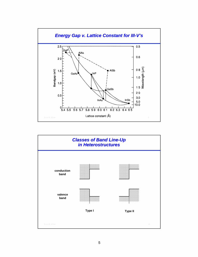
Energy Gap v. Lattice Constant for IIIEnergy Gap v. Lattice Constant for III--VV’’ss
1010D. A. B. MillerD. A. B. Miller
Classes of Band LineClasses of Band Line--UpUpin Heterostructuresin Heterostructures
conductionband
valenceband
Type I Type II

6
1111D. A. B. MillerD. A. B. Miller
Some Example Quantum Well and Some Example Quantum Well and Superlattice SystemsSuperlattice Systems
IIIIII--VV•• GaAs/GaAlAs on GaAsGaAs/GaAlAs on GaAs Type IType I•• InGaAs/InAlAs on InPInGaAs/InAlAs on InP Type IType I•• InGaAs/InP on InPInGaAs/InP on InP Type IType I•• InGaAs/GaAsInGaAs/GaAs Type I, strainedType I, strained•• InAs/GaSbInAs/GaSb Type IIType II•• GaN/GaN/AlGaNAlGaN•• GaInNAsGaInNAs/GaAs/GaAs
IIII--VIVI•• HgCdTe/CdTeHgCdTe/CdTe•• ZnSe/ZnMnSeZnSe/ZnMnSe semimagneticsemimagnetic•• CdZnTe/ZnTeCdZnTe/ZnTe Type 1, strainedType 1, strained
IVIV--VIVI•• PbTe/PbSnTePbTe/PbSnTe
IVIV•• Ge/SiGeGe/SiGe Type 1, strainedType 1, strained
1212D. A. B. MillerD. A. B. Miller
Quantum Wells and SuperlatticesQuantum Wells and Superlattices
““infiniteinfinite”” quantum wellquantum well
““particle particle in a boxin a box””
finite quantum wellfinite quantum well
particle in a particle in a box + box + ““tunnelingtunneling””penetrationpenetration
superlatticesuperlattice ““crystallographiccrystallographic”” definitiondefinitionlattice of latticeslattice of lattices
““electronicelectronic”” definitiondefinitionwells so close that wells so close that wavefunctions couple to wavefunctions couple to give give ““minibandsminibands””

7
1313D. A. B. MillerD. A. B. Miller
Particle in a BoxParticle in a Box
Schrödinger's equation (in one dimension)
φ - wavefunction of particlem - effective mass of particleV(z) - band-edge energy as a
function of z (structural potential)
φ -- wavefunction of particlewavefunction of particlemm -- effective mass of particleeffective mass of particleV(z) -- bandband--edge energy as a edge energy as a
function of function of z (structural (structural potential)potential)
Simplest case - "infinite" quantum well
Solutions
−+ =
2 2
22mddz
V z Enn n n
φ φ φa f
V z z Lz= ∞ < >, ,0V z Lz= < <0 0,
Em
nL
n A n zLn
zn
z=
− LNMOQP = =
FHGIKJ
2 2
21 2π φ π, , .... sin
1414D. A. B. MillerD. A. B. Miller
Particle in a Box Particle in a Box ((““InfiniteInfinite”” Quantum Well)Quantum Well)
n=1n=1
n=2n=2
n=3n=3
energyenergy wavefunctionwavefunction
In a semiconductor, m becomes an In a semiconductor, m becomes an effectiveeffective mass, mmass, m**, e.g., in GaAs, e.g., in GaAs•• mmee (electron effective mass) = 0.067 m(electron effective mass) = 0.067 moo (m(moo -- free electron free electron
mass)mass)Hence, e.g., for Hence, e.g., for LLzz = 100 = 100 ÅÅ, , EE11 = 38 meV (finite well calculation)= 38 meV (finite well calculation)
Lz
Em
nL
n A n zLn
zn
z=
− LNMOQP = =
FHGIKJ
2 2
21 2π φ π, , .... sin

8
1515D. A. B. MillerD. A. B. Miller
Solution for Quantum Well with Finite Solution for Quantum Well with Finite Barrier HeightBarrier Height
Boundary conditionsBoundary conditions
•• both continuous across boundaryboth continuous across boundary
•• unusual boundary conditions necessary to conserve unusual boundary conditions necessary to conserve particle flux and ensure Hermitian operatorparticle flux and ensure Hermitian operator
•• no fundamental justification for this particular boundary no fundamental justification for this particular boundary condition condition
–– these conditions are physically reasonable and give these conditions are physically reasonable and give results that usually agree well with experimentresults that usually agree well with experiment
–– this whole envelope function approach is only an this whole envelope function approach is only an approximation anywayapproximation anyway
For a discussion of envelope function models, including For a discussion of envelope function models, including discussion of the boundary conditions, see M. G. Burt, J. discussion of the boundary conditions, see M. G. Burt, J. Phys: Condens. Matter, 4, 6651Phys: Condens. Matter, 4, 6651--6690 (1992)6690 (1992)
φ φ, 1m
ddz
1616D. A. B. MillerD. A. B. Miller
Solution for Quantum Well with Finite Solution for Quantum Well with Finite Barrier HeightBarrier Height
Eigenenergies for quantum well of finite depth VEigenenergies for quantum well of finite depth Vbb solutions of solutions of
andand
where where • E1
∞ is the solution for the first level in a well of the same width is the solution for the first level in a well of the same width but with infinitely high barriersbut with infinitely high barriers
•• mw and and mb are the well and barrier effective masses respectively are the well and barrier effective masses respectively The eigenfunctions are sinusoidal in the well and exponentially The eigenfunctions are sinusoidal in the well and exponentially
decaying in the barriersdecaying in the barriersSee, e.g., C. Weisbuch in See, e.g., C. Weisbuch in ““Semiconductors and SemimetalsSemiconductors and Semimetals””, vol. , vol.
24, ed. R. Dingle, Academic Press, New York, 198724, ed. R. Dingle, Academic Press, New York, 1987
EEE
mm
V Ejj w
bb jcot π
2 1
12
12
∞
FHGIKJ
L
NMMM
O
QPPP
= − −LNM
OQPc h
EEE
mm
V Ejj w
bb jtan π
2 1
12
12
∞FHGIKJ
L
NMMM
O
QPPP
= −LNM
OQPd h
9
1717D. A. B. MillerD. A. B. Miller
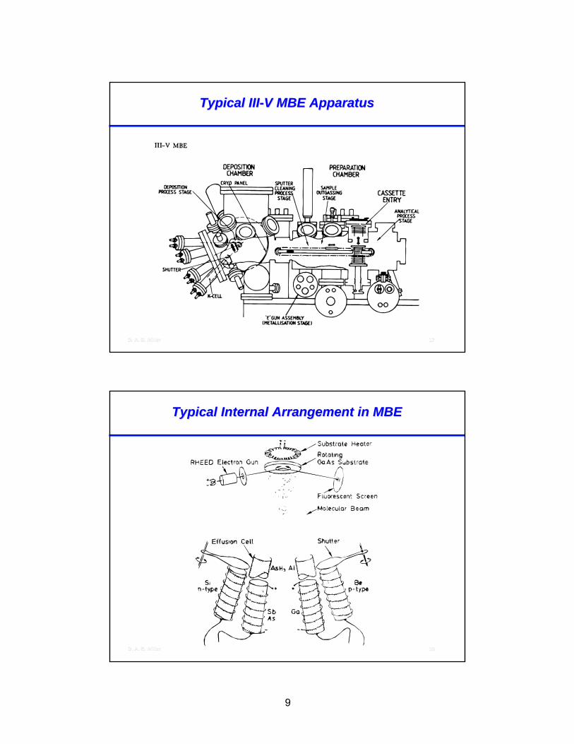
Typical IIITypical III--V MBE ApparatusV MBE Apparatus
1818D. A. B. MillerD. A. B. Miller
Typical Internal Arrangement in MBETypical Internal Arrangement in MBE

10
1919D. A. B. MillerD. A. B. Miller
LowLow--Pressure MOCVD Pressure MOCVD
2020D. A. B. MillerD. A. B. Miller
Growth of Layered Semiconductor Growth of Layered Semiconductor Structures Structures -- Some ReferencesSome References
Organometallic VaporOrganometallic Vapor--Phase Epitaxy: Theory and Practice, G. B. Phase Epitaxy: Theory and Practice, G. B. StringfellowStringfellow, 2, 2ndnd Edition (Academic Press, 1999)Edition (Academic Press, 1999)
Materials Fundamentals of Molecular Beam Epitaxy, J. Y. Tsao Materials Fundamentals of Molecular Beam Epitaxy, J. Y. Tsao (Academic Press, 1993)(Academic Press, 1993)
Molecular Beam Epitaxy : Fundamentals and Current Status, Molecular Beam Epitaxy : Fundamentals and Current Status, Marian A. Herman and H. Sitter (Springer Series in Materials Marian A. Herman and H. Sitter (Springer Series in Materials Science, Vol 7), 2nd Rev edition (Science, Vol 7), 2nd Rev edition (SpingerSpinger, 1997), 1997)

11
2121D. A. B. MillerD. A. B. Miller
Linear Optical Properties of Quantum Linear Optical Properties of Quantum WellsWells
Linear absorption (neglecting excitons)Linear absorption (neglecting excitons)•• density of states and optical absorptiondensity of states and optical absorption
ExcitonsExcitonsLinear interband absorption including excitonsLinear interband absorption including excitons
2222D. A. B. MillerD. A. B. Miller
Optical Absorption (Neglecting Excitons)Optical Absorption (Neglecting Excitons)
n=3 2 1
conduction band
valence band
EG EG
EG
n=3n=2
n=1EG
3D3D quantum wellquantum well
Absorption Absorption
Photon Energy Photon Energy
momentum conservationmomentum conservationΔΔn = 0 selection rulen = 0 selection rule+ lateral momentum + lateral momentum
conservationconservation
(E-EG)1/2

12
2323D. A. B. MillerD. A. B. Miller
Optical Absorption and ParityOptical Absorption and Parity
Dipole matrix element for
optical absorption
=
< | | >Final state wavefunction
Initial state wavefunction
Distance along optical polarization direction (e.g., x, y, or z)
< | | >even odd
z
< | | >z
=
= 0
Finite because different parity
Initial and final states must have opposite parity in direction Initial and final states must have opposite parity in direction of of interest, otherwise the integral of final state wavefunction x interest, otherwise the integral of final state wavefunction x distance x initial state wavefunction is zero.distance x initial state wavefunction is zero.
even even
a z Ab z a z Ab z dza f a f a f a f≡ ∗zWith notation
2424D. A. B. MillerD. A. B. Miller
Quantum Well Absorption and ParityQuantum Well Absorption and Parity
Actual electron or hole wavefunction is product of Actual electron or hole wavefunction is product of Envelope x Unit cellEnvelope x Unit cell
Necessary parity difference for absorption can be provided throuNecessary parity difference for absorption can be provided through unit gh unit cell or envelope functioncell or envelope function
Interband absorption Interband absorption -- parity difference provided by unit cell parity difference provided by unit cell -- SS--like like conduction band and Pconduction band and P--like valence bandlike valence band
Hence selection rule for interband absorption in quantum wellsHence selection rule for interband absorption in quantum wellsElectron and hole subband envelope function should have same parElectron and hole subband envelope function should have same parityity
x, y, or zx x
electron envelope
electron unit cell
hole envelope
hole unit cell
interband

13
2525D. A. B. MillerD. A. B. Miller
Heavy and Light HolesHeavy and Light Holesin Quantum Wellsin Quantum Wells
Note there are two kinds of holes Note there are two kinds of holes --•• heavy (e.g. 0.35 mass in GaAs)heavy (e.g. 0.35 mass in GaAs)•• light (e.g. 0.09 mass in GaAs)light (e.g. 0.09 mass in GaAs)
Consequences in quantum wells Consequences in quantum wells •• get two sets of confined hole states, therefore two sets get two sets of confined hole states, therefore two sets
of "steps" in absorption in generalof "steps" in absorption in general•• complex valence bands because of anticrossing of complex valence bands because of anticrossing of
subbandssubbands•• symmetry broken by making layered structuresymmetry broken by making layered structure
–– different masses in the plane (heavy holes lighter, different masses in the plane (heavy holes lighter, light holes heavier)light holes heavier)
–– microscopic polarization rulesmicroscopic polarization rules
2626D. A. B. MillerD. A. B. Miller
Heavy and Light Hole Selection RulesHeavy and Light Hole Selection Rules
Interband polarization selection rules (from unit cell propertieInterband polarization selection rules (from unit cell properties s and angular momentum selection rules)and angular momentum selection rules)
•• For optical electric vector in plane of layers (TE in For optical electric vector in plane of layers (TE in waveguide)waveguide)
–– both lightboth light--hole hole -- conduction and heavyconduction and heavy--hole hole --conduction transitions allowed (heavyconduction transitions allowed (heavy--hole hole --conduction stronger)conduction stronger)
•• For optical electric vector perpendicular to plane of layers For optical electric vector perpendicular to plane of layers (TM in waveguide)(TM in waveguide)
–– only light hole only light hole -- conduction transitions allowedconduction transitions allowed
•• Explains why quantum well lasers always emit in TE Explains why quantum well lasers always emit in TE polarizationpolarization

14
2727D. A. B. MillerD. A. B. Miller
Quantum Well Absorption and ParityQuantum Well Absorption and Parity
Intersubband absorption - parity difference provided by envelope functions
Hence selection rules for intersubband absorption in quantum welHence selection rules for intersubband absorption in quantum wellsls
Electron subband envelope functions should have opposite parityElectron subband envelope functions should have opposite parityOptical polarization should be perpendicular to the quantum wellOptical polarization should be perpendicular to the quantum well layerslayers
•• therefore does not work for normal incidence therefore does not work for normal incidence -- need waveguide, need waveguide, grating, or other special coupling schemegrating, or other special coupling scheme
Note: for valence intersubband transitions, can operate at normaNote: for valence intersubband transitions, can operate at normal incidence l incidence because of valence band mixing of unit cell wavefunctions (see, because of valence band mixing of unit cell wavefunctions (see, e.g., Y. C. e.g., Y. C. Chang and R. B. James, Phys. Rev. B39, 12672 (1989))Chang and R. B. James, Phys. Rev. B39, 12672 (1989))
zx xelectron envelope
electron unit cell
electron unit cell
electron envelope
intersubband
2828D. A. B. MillerD. A. B. Miller
Quantum Well Intersubband Infrared Quantum Well Intersubband Infrared DetectorDetector
•• must have electrons in well (by doping or injection)must have electrons in well (by doping or injection)•• transition raises electron from ground state to excited state ortransition raises electron from ground state to excited state or continuum continuum
above barrier, from where it can move to give photocurrentabove barrier, from where it can move to give photocurrent•• light must be polarized perpendicular to the quantum well layerslight must be polarized perpendicular to the quantum well layers for for
absorption, so simple normal incidence will not workabsorption, so simple normal incidence will not work•• transitions in midtransitions in mid--infrared (e.g., 10 microns wavelength)infrared (e.g., 10 microns wavelength)
B. F. Levine et al., Appl. Phys. Lett. 50, 1093 (1987); 54, 2704B. F. Levine et al., Appl. Phys. Lett. 50, 1093 (1987); 54, 2704 (1989)(1989)

15
2929D. A. B. MillerD. A. B. Miller
Quantum Well Intersubband Infrared Quantum Well Intersubband Infrared Detectors Detectors -- Some General ReferencesSome General References
QuantumQuantum--well infrared photodetectors, B. F. Levine, J. Appl. well infrared photodetectors, B. F. Levine, J. Appl. Phys. Phys. 7474, R1, R1--R81 (1993)R81 (1993)
Intersubband Transitions in Quantum Wells, ed. E. Rosencher, B. Intersubband Transitions in Quantum Wells, ed. E. Rosencher, B. Vinter, and B. Levine, Plenum, New York, 1992Vinter, and B. Levine, Plenum, New York, 1992
Semiconductor Quantum Wells and Superlattices for LongSemiconductor Quantum Wells and Superlattices for Long--Wavelength Infrared Detectors, ed. M. O. Manasreh, Artech Wavelength Infrared Detectors, ed. M. O. Manasreh, Artech House, Boston, 1993House, Boston, 1993
Comparison of the performance of quantum well and Comparison of the performance of quantum well and conventional bulk infrared photodetectors, A. conventional bulk infrared photodetectors, A. RogalskiRogalski, , Infrared Physics and Technology, Infrared Physics and Technology, 3838, 295, 295--310 (1997)310 (1997)
3030D. A. B. MillerD. A. B. Miller
Room Temperature Absorption Spectra of Room Temperature Absorption Spectra of Quantum WellsQuantum Wells
•• shows clear shows clear ““stepstep””structure structure
•• shows also shows also sharp peakssharp peaks
16
3131D. A. B. MillerD. A. B. Miller
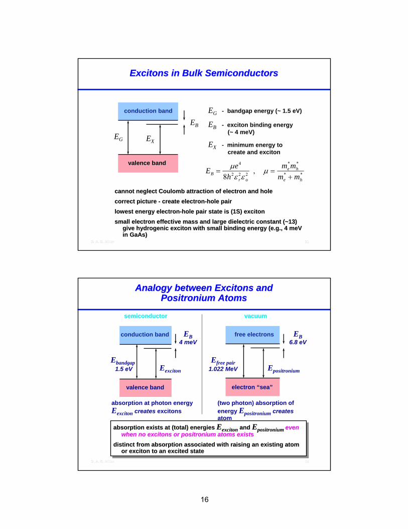
Excitons in Bulk SemiconductorsExcitons in Bulk Semiconductors
conduction bandconduction band
valence bandvalence band
EX
EB
EG
EG - bandgap energy (~ 1.5 eV)
EB - exciton binding energy (~ 4 meV)
EX - minimum energy to create and exciton
cannot neglect Coulomb attraction of electron and hole cannot neglect Coulomb attraction of electron and hole correct picture correct picture -- create electroncreate electron--hole pairhole pairlowest energy electronlowest energy electron--hole pair state is (1S) excitonhole pair state is (1S) excitonsmall electron effective mass and large dielectric constant (~13small electron effective mass and large dielectric constant (~13) )
give hydrogenic exciton with small binding energy (e.g., 4 meV give hydrogenic exciton with small binding energy (e.g., 4 meV in GaAs)in GaAs)
E eh
m mm mB
r o
e h
e h
= =+
με ε
μ4
2 2 28,
* *
* *
3232D. A. B. MillerD. A. B. Miller
Analogy between Excitons and Analogy between Excitons and Positronium AtomsPositronium Atoms
absorption exists at (total) energies Eexciton and Epositronium even when no excitons or positronium atoms exists
distinct from absorption associated with raising an existing atom or exciton to an excited state
absorption exists at (total) energies absorption exists at (total) energies EEexcitonexciton and and EEpositronium positronium even even when no excitons or positronium atoms existwhen no excitons or positronium atoms existss
distinct from absorption associated with raising an existing atodistinct from absorption associated with raising an existing atom m or exciton to an excited stateor exciton to an excited state
conduction bandconduction band
valence bandvalence band
Eexciton
EB4 meV
Ebandgap1.5 eV
free electronsfree electrons
electron electron ““seasea””
Epositronium
EB6.8 eV
Efree pair1.022 MeV
semiconductorsemiconductor vacuumvacuum
absorption at photon energy Eexciton creates excitons
(two photon) absorption of energy Epositronium createsatom

17
3333D. A. B. MillerD. A. B. Miller
Excitons in Quantum WellsExcitons in Quantum Wells
300 300 ÅÅ 100 100 ÅÅExciton in bulk GaAsExciton in bulk GaAs Exciton in quantum wellExciton in quantum well
Confinement of the exciton in the quantum well makes the excitonConfinement of the exciton in the quantum well makes the excitonsmaller in smaller in allall directions (tries to remain nearly spherical)directions (tries to remain nearly spherical)
Excitons strong at room temperature in quantum wells becauseExcitons strong at room temperature in quantum wells because•• smaller exciton smaller exciton ““orbits fasterorbits faster””, completing orbit before being , completing orbit before being
destroyed by a phonon destroyed by a phonon •• electron and hole are closer in the smaller exciton (binding electron and hole are closer in the smaller exciton (binding
energy now ~ 10 meV), hence the optical absorption is energy now ~ 10 meV), hence the optical absorption is strongerstronger
3434D. A. B. MillerD. A. B. Miller
Wavelength Selective DetectorWavelength Selective Detector
detects short wavelength while rejecting longer wavelength
quantum well “samples” particular point in standing wave pattern formed by mirror reflection
L. Carraresi et al., Appl. Phys. Lett. 64, 134-136 (1994); D. A. B. Miller "Laser Tuners and Wavelength-Sensitive Detectors Based on Absorbers in Standing Waves" IEEE J. Quantum Electron. 30, 732-749 (1994)
AR Coating
200 Å p doped GaAs
3500 Å p doped
1500 Å undoped
Al0.2 Ga0.8 As / GaAs (30Å/30Å) SL
50 Å Al0.4 Ga0.6 As undoped
110 Å GaAs undoped quantum well
50 Å Al0.4 Ga0.6 As undoped
1000 Å Al0.3 Ga0.7 As undoped
2500 Å Al0.4 Ga0.6 As / GaAs (30Å/30Å) SLundoped
2.3 μm Al0.2 Ga0.8 As n doped
723 Å AlAs599 Å Al0.11 Ga0.89 As x15 n doped
mirror @ 8500 Å
GaAs n doped substrate
Gold contact
Silver contact
ZUVW
UVW
p
i
nStanding wave intensity
820 830 840 850 860 870
Phot
ocur
rent
(a.u
.)
Wavelength (nm)
QW at standing
wave minimum
QW at standing
wave minimum
18
3535D. A. B. MillerD. A. B. Miller
Quantum Well LasersQuantum Well Lasers
history of threshold current densitieshistory of threshold current densitieshomojunctionshomojunctionsdouble heterojunctionsdouble heterojunctionsseparate confinement heterostructuresseparate confinement heterostructuresquantum mechanical benefits of quantum wellsquantum mechanical benefits of quantum wellseffects of straineffects of strain
vertical cavity lasersvertical cavity lasersquantum cascade lasersquantum cascade lasers
3636D. A. B. MillerD. A. B. Miller
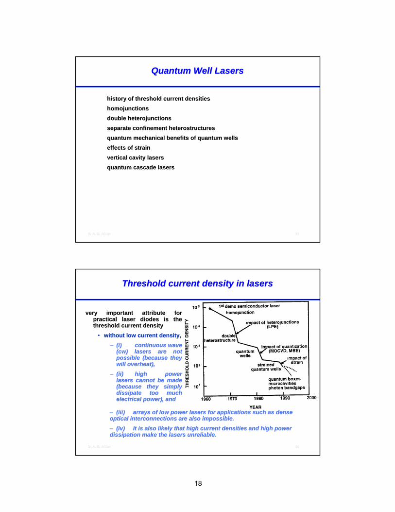
Threshold current density in lasers Threshold current density in lasers
very important attribute for very important attribute for practical laser diodes is the practical laser diodes is the threshold current densitythreshold current density
•• without low current density, without low current density, –– (i) (i) continuous wave continuous wave
(cw) lasers are not (cw) lasers are not possible (because they possible (because they will overheat), will overheat),
–– (ii)(ii) high power high power lasers cannot be made lasers cannot be made (because they simply (because they simply dissipate too much dissipate too much electrical power), and electrical power), and
–– (iii) (iii) arrays of low power lasers for applications such as dense arrays of low power lasers for applications such as dense optical interconnections are also impossible. optical interconnections are also impossible.
–– (iv)(iv) It is also likely that high current densities and high power It is also likely that high current densities and high power dissipation make the lasers unreliable.dissipation make the lasers unreliable.

19
3737D. A. B. MillerD. A. B. Miller
Homojunction laserHomojunction laser
"edge"edge--emitting" waveguide laser emitting" waveguide laser
large gain along the junction large gain along the junction •• gain material is long in this directiongain material is long in this direction
natural reflectivity semiconductor surfaces (~ 30%)natural reflectivity semiconductor surfaces (~ 30%)•• natural surfaces can be relatively easily formed exactly plane anatural surfaces can be relatively easily formed exactly plane and nd
parallel by performing "cleaves" along crystallographic directioparallel by performing "cleaves" along crystallographic directions.ns.
3838D. A. B. MillerD. A. B. Miller
Homojunction laserHomojunction laser
homojunction homojunction -- made from only one materialmade from only one materialto turn GaAs from being absorbing to having enough gain to run to turn GaAs from being absorbing to having enough gain to run
a semiconductor laser a semiconductor laser
•• requires ~ 10requires ~ 101818 cmcm--33 carrier density carrier density if we try to make a laser all from GaAsif we try to make a laser all from GaAs
•• might end up with a layer of about 3 microns thickness might end up with a layer of about 3 microns thickness (thick enough to contain a lasing mode)(thick enough to contain a lasing mode)
–– lifetime of the carriers, e.g., due to spontaneous lifetime of the carriers, e.g., due to spontaneous emission, is typically ~3 nsemission, is typically ~3 ns
•• to sustain 10to sustain 101818 cmcm--33 carriers in this volume requires a carriers in this volume requires a current density of current density of
–– 10101818 x 3 x 10x 3 x 10--44/(3 x 10/(3 x 10--99) = 10) = 102323 carriers/cmcarriers/cm22 per second, per second,
•• ~ 1.6 x 10~ 1.6 x 1044 A/cmA/cm22
–– ~ 30 kW/cm~ 30 kW/cm22 even assuming only 2V operating even assuming only 2V operating voltagevoltage

20
3939D. A. B. MillerD. A. B. Miller
Double heterostructure laserDouble heterostructure laser
first major piece of quantum mechanical first major piece of quantum mechanical and optical engineering to reduce the and optical engineering to reduce the threshold threshold -- double heterostructuredouble heterostructure
•• relatively thick (e.g., 0.1 relatively thick (e.g., 0.1 -- 1 micron) 1 micron) GaAs layerGaAs layer
–– sandwiched between sandwiched between •• two wider bandgap AlGaAs two wider bandgap AlGaAs
layerslayersAlGaAs layers perform a double role. AlGaAs layers perform a double role.
•• have lower refractive index than the have lower refractive index than the GaAs layerGaAs layer
–– the three layers can form a the three layers can form a waveguidewaveguide
•• second role of the AlGaAs layerssecond role of the AlGaAs layers–– electrons & holes both see lower electrons & holes both see lower
energy in GaAs layerenergy in GaAs layer•• tend to be confined within tend to be confined within
this thin layerthis thin layer–– more likely will combine more likely will combine
radiatively radiatively
4040D. A. B. MillerD. A. B. Miller
Threshold and layer thicknessThreshold and layer thickness
index difference between the GaAs and the AlGaAs can be index difference between the GaAs and the AlGaAs can be moderately large moderately large
•• e.g., index ~ 3.6 for GaAs, ~ 3.46 for Ale.g., index ~ 3.6 for GaAs, ~ 3.46 for Al0.20.2GaGa0.80.8As at 870 nmAs at 870 nm
optical mode can be confined even down to GaAs thicknesses ~ optical mode can be confined even down to GaAs thicknesses ~ 0.1 micron0.1 micron
•• overlap of the mode, Eoverlap of the mode, Eopop, with the gain region is still good, with the gain region is still goodinstead of having to invert 3 microns thickness of materialinstead of having to invert 3 microns thickness of material
•• only have to invert about a factor of 10 less materialonly have to invert about a factor of 10 less material
–– reduces the threshold current density by ~ x 10. reduces the threshold current density by ~ x 10.
further thinning only continues to reduce the threshold if the further thinning only continues to reduce the threshold if the optical mode remains substantially confined within itoptical mode remains substantially confined within it
•• if the layer becomes substantially thinner than the optical if the layer becomes substantially thinner than the optical modemode
–– mode as a whole does not see as much gainmode as a whole does not see as much gain
21
4141D. A. B. MillerD. A. B. Miller
Threshold and layer thicknessThreshold and layer thickness
if we had no other cavity losses, if we had no other cavity losses, •• e.g., 100% reflecting mirrors and no intracavity absorption othee.g., 100% reflecting mirrors and no intracavity absorption other than in r than in
the GaAs layerthe GaAs layer
–– would not matter what the mode size waswould not matter what the mode size was
•• only be necessary to get the GaAs material above transparency only be necessary to get the GaAs material above transparency to obtain lasingto obtain lasing
hence the less material thickness there was, the lower the threshence the less material thickness there was, the lower the threshold current hold current density would be. density would be.
in practice always is some loss in practice always is some loss •• in the cladding materialsin the cladding materials
–– e.g., due to intersubband absorption in the p doped layerse.g., due to intersubband absorption in the p doped layers
•• much more convenient to work with natural reflectivity end mirromuch more convenient to work with natural reflectivity end mirrors for rs for edgeedge--emitting lasersemitting lasers
hence in practice, very thin layers with consequent very poor ovhence in practice, very thin layers with consequent very poor overlap with the erlap with the gain region would lead to higher threshold currents eventually. gain region would lead to higher threshold currents eventually.
4242D. A. B. MillerD. A. B. Miller
Separate confinement heterostructuresSeparate confinement heterostructures
in the separate confinement heterostructure (SCH), in the separate confinement heterostructure (SCH), •• build a thicker, transparent, waveguide "core" layer to confine build a thicker, transparent, waveguide "core" layer to confine the the
wave,wave,
–– put the thin gain region in the center of this layerput the thin gain region in the center of this layer
•• hence we can continue to decrease the gain layer thickness withohence we can continue to decrease the gain layer thickness without ut making the mode bigger, thereby further reducing the threshold making the mode bigger, thereby further reducing the threshold current density. current density.
technically feasible because sophisticated layered semiconductortechnically feasible because sophisticated layered semiconductor growth growth techniques such as molecular beam epitaxy (MBE) and metaltechniques such as molecular beam epitaxy (MBE) and metal--organic organic chemical vapor deposition (MOCVD)chemical vapor deposition (MOCVD)
•• simple SCH has a step in the bandgap energy and indexsimple SCH has a step in the bandgap energy and index•• more sophisticated version, the graded index SCH (GRINSCH), has more sophisticated version, the graded index SCH (GRINSCH), has
sloping wallssloping walls–– gain regions are also quantum wells (e.g., 10 nm thickness), andgain regions are also quantum wells (e.g., 10 nm thickness), and
additionally show quantum confinement effects additionally show quantum confinement effects

22
4343D. A. B. MillerD. A. B. Miller
Separate confinement heterostructuresSeparate confinement heterostructures
4444D. A. B. MillerD. A. B. Miller
Quantum mechanical benefits of quantum Quantum mechanical benefits of quantum well well -- density of statesdensity of states
instead of having a smoothly rising (joint) density of states, tinstead of having a smoothly rising (joint) density of states, the quantum well he quantum well has "steps"has "steps"
•• more efficient at using the carriers to obtain gainmore efficient at using the carriers to obtain gain
–– carriers have the largest occupation probabilities at the lowestcarriers have the largest occupation probabilities at the lowestenergies because of their thermal distributionenergies because of their thermal distribution
•• in the bulk, the occupation probabilities are highest obviously in the bulk, the occupation probabilities are highest obviously at the bottom of the bands, but the density of states there is at the bottom of the bands, but the density of states there is lowlow
–– gain actually peaks at a somewhat higher energy because, gain actually peaks at a somewhat higher energy because, though the thermal occupation probabilities are lower, the though the thermal occupation probabilities are lower, the density of states is higher, resulting in more gaindensity of states is higher, resulting in more gain
in the case of the quantum wellin the case of the quantum well
•• density of states is also high at the lowest possible carrier endensity of states is also high at the lowest possible carrier energiesergies–– peak in the gain therefore occurs for the states with the highespeak in the gain therefore occurs for the states with the highest t
thermal occupation probabilities, leading to more efficient use thermal occupation probabilities, leading to more efficient use of of carriers to obtain gaincarriers to obtain gain

23
4545D. A. B. MillerD. A. B. Miller
Quantum Well Lasing GainQuantum Well Lasing Gain
The distribution of injected carriers in bulk and QW structures need to achieve the same peak gain spectra, as shown below
Schematic diagrams of the density of states for bulk material and QW hetero-structures
Because of their abrupt density of states, quantum wells give more gain for a given carrier density at a finite temperature(After W. T. Tsang)
see, for example, “Quantum Well Lasers”, ed. P. S. Zory, Academic, Boston, 1993
4646D. A. B. MillerD. A. B. Miller
Quantum well laser differential gainQuantum well laser differential gain
quantum well obtains the same gain for almost a factor of two quantum well obtains the same gain for almost a factor of two less carrier densityless carrier density
•• also leads to a better differential gain (increase in gain per also leads to a better differential gain (increase in gain per unit carrier density)unit carrier density)
–– important for various aspects of performance, important for various aspects of performance, including including
•• highhigh--frequency modulation capability and frequency modulation capability and •• reduction of the relative effects of "chirp" (change reduction of the relative effects of "chirp" (change
of refractive index under modulation).of refractive index under modulation).other mechanisms that further increase the gain per carrier alsoother mechanisms that further increase the gain per carrier also
further improve differential gainfurther improve differential gain

24
4747D. A. B. MillerD. A. B. Miller
Strain and Valence Band StructureStrain and Valence Band Structure
conduction and valence bands without strain
valence bands with biaxial compressive strain
valence bands with biaxial tensile strain
strain also gives highly anisotropic valence bands
E. P. O’Reilly “Valence band engineering in strained-layer structures” Semicond. Sci. Technol. 4, 121-137 (1989)
4848D. A. B. MillerD. A. B. Miller
Lattice mismatch and allowed layer thicknessLattice mismatch and allowed layer thickness
can grow very thin layers even when there is substantial latticecan grow very thin layers even when there is substantial latticemismatchmismatch
•• useful for making highuseful for making high--performance lasers performance lasers •• surprisingly reliable despite the very large strains in the surprisingly reliable despite the very large strains in the
lattice in the thin "quantum well" layer.lattice in the thin "quantum well" layer.

25
4949D. A. B. MillerD. A. B. Miller
Strain and Quantum Well LasersStrain and Quantum Well Lasers
strain makes the valence bands very anisotropicstrain makes the valence bands very anisotropic•• in particular, it makes the effective mass of valence band lowerin particular, it makes the effective mass of valence band lower in the plane of in the plane of
the quantum wells (even for the case where the the quantum wells (even for the case where the ““heavy holeheavy hole”” is the upper is the upper subband)subband)
lower hole effective mass makes the valence band more like the clower hole effective mass makes the valence band more like the conduction bandonduction band•• makes the hole distribution more makes the hole distribution more ““FermiFermi--DiracDirac”” (pushes Fermi level into the (pushes Fermi level into the
band)band)•• improves probability of finding electron in conduction band and improves probability of finding electron in conduction band and hole in valence hole in valence
band in same kband in same k--statestate•• hence improves gain (e.g., theoretically reduces threshold up tohence improves gain (e.g., theoretically reduces threshold up to factor of ~ 5)factor of ~ 5)
A. R. Adams, Electron. Lett. 22, 249 (1986); E. Yablonovich and A. R. Adams, Electron. Lett. 22, 249 (1986); E. Yablonovich and E. O. Kane, J. Lightwave E. O. Kane, J. Lightwave Technol. LTTechnol. LT--4, 504 (1986); J. J. Coleman et al. IEEE J. Quantum Electron. 284, 504 (1986); J. J. Coleman et al. IEEE J. Quantum Electron. 28, 1983 , 1983 (1992)(1992)
large hole mass~ Boltzmann distribution
small hole mass~ degenerate Fermi-Dirac distribution
5050D. A. B. MillerD. A. B. Miller
Improvement in matrix element Improvement in matrix element
In the bulk material, there is no distinction between the x, y, In the bulk material, there is no distinction between the x, y, and z directions.and z directions.•• holes occupy P states with x, y, and z character with equal likeholes occupy P states with x, y, and z character with equal likelihoodlihood
–– only states associated with a particular direction can give riseonly states associated with a particular direction can give rise to to optical emission in that direction, and so optical emission in that direction, and so
•• only 1/3 of eonly 1/3 of e--h pairs contribute to gain in any one polarization.h pairs contribute to gain in any one polarization.In a biaxially compressively strained materialIn a biaxially compressively strained material
•• upper band is heavy hole likeupper band is heavy hole like–– this band has no z like character, and has equal x and y charactthis band has no z like character, and has equal x and y character. er.
•• half of ehalf of e--h pairs can contribute to gain in x or y polarizations, h pairs can contribute to gain in x or y polarizations, –– an improvement over the 1/3 in the bulk.an improvement over the 1/3 in the bulk.
In a biaxially tensile strained materialIn a biaxially tensile strained material•• upper band is light holeupper band is light hole
–– has 2/3 z like characterhas 2/3 z like character•• so 2 of 3 eso 2 of 3 e--h pairs contribute to gain for polarization in z h pairs contribute to gain for polarization in z
direction, direction, –– factor of 2 improvement over the bulk casefactor of 2 improvement over the bulk case
•• more careful analysis includes mixing with the splitmore careful analysis includes mixing with the split--off bandoff band

26
5151D. A. B. MillerD. A. B. Miller
Vertical Cavity Surface Emitting LaserVertical Cavity Surface Emitting Laser
very high reflectivity Braggvery high reflectivity Bragg--reflector mirrors allow very thin gain reflector mirrors allow very thin gain region, and potentially low thresholdregion, and potentially low threshold
can be single quantum wellcan be single quantum wellInGaAs quantum well allows emission through GaAs substrateInGaAs quantum well allows emission through GaAs substratesee, e.g., C. J. Changsee, e.g., C. J. Chang--Hasnain, Hasnain, ““Vertical Cavity SurfaceVertical Cavity Surface--Emitting Emitting
LasersLasers”” in in ““Semiconductor Lasers, Past, Present, and FutureSemiconductor Lasers, Past, Present, and Future””, , ed. G. P. Agrawal (AIP,1995)ed. G. P. Agrawal (AIP,1995)
5252D. A. B. MillerD. A. B. Miller
OxideOxide--confined VCSELconfined VCSEL
Oxidation of AlAs to Oxidation of AlAs to AlOAlO gives insulator to confine current gives insulator to confine current flowflow
E.g., 290 microamp thresholdE.g., 290 microamp threshold27% wall plug efficiency at 1 mW output27% wall plug efficiency at 1 mW outputWeigl et al. IEEE Photonics Technol. Lett. 8, 971 Weigl et al. IEEE Photonics Technol. Lett. 8, 971 -- 973 (1996)973 (1996)
27
5353D. A. B. MillerD. A. B. Miller
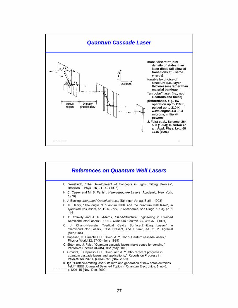
Quantum Cascade LaserQuantum Cascade Laser
more “discrete” joint density of states than laser diode (all allowed transitions at ~ same energy)
tunable by choice of structure (i.e., layer thicknesses) rather than material bandgap
“unipolar” laser (i.e., not electrons and holes)
performance, e.g., cw operation up to 110 K, pulsed up to 210 K, wavelengths 4.3 - 8.4 microns, milliwatt powers
J. Faist et al., Science, 264, 553 (1994); C. Sirtori et al., Appl. Phys. Lett. 68 1745 (1996)
5454D. A. B. MillerD. A. B. Miller
References on Quantum Well LasersReferences on Quantum Well Lasers
C. Weisbuch, "The Development of Concepts in Light-Emitting Devices", Brazilian J. Phys., 26, 21 - 42 (1996)
H. C. Casey and M. B. Panish, Heterostructure Lasers (Academic, New York, 1978)
K. J. Ebeling, Integrated Optoelectronics (Springer-Verlag, Berlin, 1993)C. H. Henry, "The origin of quantum wells and the quantum well laser", in
Quantum well lasers, ed. P. S. Zory, Jr. (Academic, San Diego, 1993), pp. 1 - 16
E. P. O'Reilly and A. R. Adams, "Band-Structure Engineering in Strained Semiconductor Lasers", IEEE J. Quantum Electron. 30, 366-379 (1994)
C. J. Chang-Hasnain, “Vertical Cavity Surface-Emitting Lasers” in “Semiconductor Lasers, Past, Present, and Future”, ed. G. P. Agrawal (AIP,1995)
F. Capasso, C. Gmachl, D. L. Sivco, A. Y. Cho “Quantum cascade lasers,”Physics World 12, 27-33 (June 1999)
C. Sirtori and J. Faist, “Quantum cascade lasers make sense for sensing,”Photonics Spectra 34 (#5), 162 (May 2000)
C. Gmachl, F. Capasso, D. L. Sivco, and A. Y. Cho, “Recent progress in quantum cascade lasers and applications,” Reports on Progress in Physics, 64, no.11, p.1533-601 ((Nov. 2001)
K. Iga, “Surface-emitting laser - its birth and generation of new optoelectronics field,” IEEE Journal of Selected Topics in Quantum Electronics, 6, no.6, p.1201-15 ((Nov.-Dec. 2000)

28
5555D. A. B. MillerD. A. B. Miller
Nonlinear Optics and Nonlinear Optics and Electrooptics of Quantum Wells Electrooptics of Quantum Wells
Interband Nonlinear Optics Near the BandgapInterband Nonlinear Optics Near the Bandgap•• Nonlinear absorptionNonlinear absorption•• Applications to modelocking and switchingApplications to modelocking and switching
Quantum Well Electroabsorption PhysicsQuantum Well Electroabsorption Physics•• Fields parallel to the layersFields parallel to the layers•• Fields perpendicular to the layers (quantumFields perpendicular to the layers (quantum--confined Stark confined Stark
effect)effect)
5656D. A. B. MillerD. A. B. Miller
Nonlinear AbsorptionNonlinear Absorption
low intensitylow intensitylow intensity
high intensityhigh intensityhigh intensity

29
5757D. A. B. MillerD. A. B. Miller
How Do Excitons or Free Electrons and How Do Excitons or Free Electrons and Holes Change the Optical PropertiesHoles Change the Optical Properties
Filling of states (Filling of states (““simplesimple”” saturation)saturation)•• Pauli exclusion means there is a limit to the number of Pauli exclusion means there is a limit to the number of
electrons and holes (carriers) or excitons in a given volume electrons and holes (carriers) or excitons in a given volume within a given energy range, e.g., excitons or free carriers within a given energy range, e.g., excitons or free carriers filling spacefilling space
excitons filling spaceexcitons filling space free carriers filling spacefree carriers filling space•• ““saturationsaturation”” when no space left to put excitons without them when no space left to put excitons without them
overlapping with another exciton or free carrier overlapping with another exciton or free carrier -- probability of probability of creating exciton then small so absorption must reducecreating exciton then small so absorption must reduce
•• occurs at densities of approximately one exciton or free carrieroccurs at densities of approximately one exciton or free carrierpair per exciton volume (e.g. 10 pair per exciton volume (e.g. 10 1717 cm cm --33))
D. S. Chemla et al., IEEE J. Quantum Electron. 20, 265 (1984); SD. S. Chemla et al., IEEE J. Quantum Electron. 20, 265 (1984); S. . SchmittSchmitt--Rink et al., Phys. Rev. B32, 6601 (1985) Rink et al., Phys. Rev. B32, 6601 (1985)
5858D. A. B. MillerD. A. B. Miller
How Do Excitons or Free Electrons and How Do Excitons or Free Electrons and Holes Change the Optical PropertiesHoles Change the Optical Properties
Change in nature of states, e.g.,Change in nature of states, e.g.,•• change in energy change in energy
–– e.g., bandgap renormalizatione.g., bandgap renormalization
•• change in size or shape of the excitonchange in size or shape of the excitonbyby
•• direct Coulomb screening direct Coulomb screening
–– e.g., electrons and holes change the dielectric e.g., electrons and holes change the dielectric constant, hence changing the excitonconstant, hence changing the exciton
•• exchange screening exchange screening –– because of Pauli exclusion, the electrons are further because of Pauli exclusion, the electrons are further
apart than would be calculated classically, so the apart than would be calculated classically, so the screening is different from that calculated classicallyscreening is different from that calculated classically
Also occurs at densities of approximately one exciton or free Also occurs at densities of approximately one exciton or free carrier pair per exciton volume (e.g. 10 carrier pair per exciton volume (e.g. 10 1717 cm cm --33))
S. SchmittS. Schmitt--Rink et al., Phys. Rev. B32, 6601 (1985)Rink et al., Phys. Rev. B32, 6601 (1985)

30
5959D. A. B. MillerD. A. B. Miller
Saturable Bragg ReflectorSaturable Bragg Reflector
single quantum well gives enough absorption and saturation to mosingle quantum well gives enough absorption and saturation to modelock many delock many solid state laserssolid state lasers
incorporation into cavity end mirror gives very low excess lossincorporation into cavity end mirror gives very low excess losspositioning in end mirror gives control of amount of absorption positioning in end mirror gives control of amount of absorption and saturationand saturationS. Tsuda et al., Optics Lett. 20, 1406 (1995)S. Tsuda et al., Optics Lett. 20, 1406 (1995)
Single QW
GaAs
100
Al%
AlAs/AlGaAs Bragg Reflector
015
field penetration
750 800 850 900 950 10000
20
40
60
80
100
Ref
lect
ivity
(%)
Wavelength (nm)
x
6060D. A. B. MillerD. A. B. Miller
Laser Modelocking with Quantum Well Laser Modelocking with Quantum Well Saturable Absorbers Saturable Absorbers -- Some ReferencesSome References
Recent review: Recent review: ““Semiconductor Saturable Absorber Mirrors (SESAMSemiconductor Saturable Absorber Mirrors (SESAM’’s) for s) for Femtosecond to Nanosecond Pulse Generation in SolidFemtosecond to Nanosecond Pulse Generation in Solid--State Lasers,State Lasers,”” U. Keller U. Keller et al., IEEE J. Selected Topics Quantum Electron. 2, 435 et al., IEEE J. Selected Topics Quantum Electron. 2, 435 -- 453 (1996)453 (1996)
Other papers:Other papers:Mode locking of semiconductor diode lasers using saturable excitMode locking of semiconductor diode lasers using saturable excitonic onic
nonlinearities, P. W. Smith et al., J. Opt. Soc. Am. B2, 1228 (1nonlinearities, P. W. Smith et al., J. Opt. Soc. Am. B2, 1228 (1985)985)Color center lasers passively mode locked by quantum wells, M. NColor center lasers passively mode locked by quantum wells, M. N. Islam et al., . Islam et al.,
IEEE J. Quantum Electron. 25, 2454 (1989); see also Bulk semiconIEEE J. Quantum Electron. 25, 2454 (1989); see also Bulk semiconductor ductor saturable absorber for a NaCl color center laser, C. E. Soccolicsaturable absorber for a NaCl color center laser, C. E. Soccolich et al., Appl. h et al., Appl. Phys. Lett. 56, 2177 (1990)Phys. Lett. 56, 2177 (1990)
CoupledCoupled--cavity resonant passive modecavity resonant passive mode--locked Ti:sapphire laser, U. Keller et al., locked Ti:sapphire laser, U. Keller et al., Optics Lett. 15, 1377 (1990)Optics Lett. 15, 1377 (1990)
Subpicosecond monolithic collidingSubpicosecond monolithic colliding--pulse modepulse mode--locked multiple quantum well locked multiple quantum well lasers, Y. K. Chen et al., Appl. Phys. Lett. 58, 1253 (1991)lasers, Y. K. Chen et al., Appl. Phys. Lett. 58, 1253 (1991)
Femtosecond pulses from a continuously selfFemtosecond pulses from a continuously self--starting passively modestarting passively mode--locked locked Ti:sapphire laser, U. Keller et al., Optics Lett. 16, 1022 (1991Ti:sapphire laser, U. Keller et al., Optics Lett. 16, 1022 (1991))
SolidSolid--state lowstate low--loss intracavity saturable absorber for Nd:YLF lasers: an loss intracavity saturable absorber for Nd:YLF lasers: an antiresonant semiconductor Fabryantiresonant semiconductor Fabry--Perot saturable absorber" U. Keller et al., Perot saturable absorber" U. Keller et al., Optics Letters, 17, 505 Optics Letters, 17, 505 -- 507 (1992)507 (1992)
Recent developments in compact ultrafast lasers Recent developments in compact ultrafast lasers U. Keller, Nature, 424, no.6950, p.831U. Keller, Nature, 424, no.6950, p.831--838 (2003) 838 (2003)

31
6161D. A. B. MillerD. A. B. Miller
Quantum Well Electroabsorption PhysicsQuantum Well Electroabsorption Physics
fields parallel to the layersfields parallel to the layers•• effects similar to bulk semiconductorseffects similar to bulk semiconductors
–– exciton broadens with fieldexciton broadens with field
fields perpendicular to the layersfields perpendicular to the layers
•• effects different to bulk semiconductorseffects different to bulk semiconductors–– excitons shifts with fieldexcitons shifts with field
•• quantumquantum--confined Stark effectconfined Stark effect
6262D. A. B. MillerD. A. B. Miller
Excitons in Electric FieldsExcitons in Electric Fields
Coulomb potential of electron and hole
Coulomb potential Coulomb potential of electron and holeof electron and hole
without field
without without fieldfield
with field
with with fieldfield
exciton has 10 meV binding energy, 100 exciton has 10 meV binding energy, 100 ÅÅ diameterdiameter
•• 10 meV / 100 10 meV / 100 ÅÅ = 10= 10 44 V / cm = 1 V / V / cm = 1 V / μμmm
so easy to apply so easy to apply ““strongstrong”” field to excitonfield to excitonIn bulk semiconductors and In bulk semiconductors and in quantum wells in quantum wells with the field in the with the field in the
plane of the layersplane of the layers
•• rapid field ionization of excitonrapid field ionization of exciton•• broadening of exciton absorption line by uncertainty broadening of exciton absorption line by uncertainty
principleprinciple•• very little Stark shift (limited to about 10% of binding energy)very little Stark shift (limited to about 10% of binding energy)

32
6363D. A. B. MillerD. A. B. Miller
Effect of Parallel Fields onEffect of Parallel Fields onMultiple Quantum Well AbsorptionMultiple Quantum Well Absorption
D. A. B. Miller D. A. B. Miller et al., Phys. et al., Phys. Rev. B32, Rev. B32, 1043 (1985)1043 (1985)
0 V / cm0 V / cm0 V / cm
16 kV / cm16 kV / cm16 kV / cm
48 kV / cm48 kV / cm48 kV / cm
exciton absorption peaks broaden with fieldexciton absorption peaks broaden with field
electric fields electric fields parallelparallel to the quantum well layersto the quantum well layers
6464D. A. B. MillerD. A. B. Miller
QuantumQuantum--Confined Stark EffectConfined Stark Effect
D. A. B. Miller et D. A. B. Miller et al., Phys. Rev. al., Phys. Rev. B32, 1043 (1985)B32, 1043 (1985)
10 4 V / cm (0 V)1010 44 V / cm (0 V)V / cm (0 V)
4.7 x 10 4 V / cm (6 V)4.7 x 104.7 x 10 44 V / cm (6 V)V / cm (6 V)
7.3 x 10 4 V / cm (10 V)7.3 x 107.3 x 10 44 V / cm (10 V)V / cm (10 V)
95 95 ÅÅ GaAs GaAs quantum wellsquantum wells
exciton absorption peaks shift with fieldexciton absorption peaks shift with field
electric fields electric fields perpendicularperpendicular to the quantum well layersto the quantum well layers

33
6565D. A. B. MillerD. A. B. Miller
Effects of Perpendicular Fields on Effects of Perpendicular Fields on Quantum Well AbsorptionQuantum Well Absorption
Exciton resonances still observed at high fields becauseExciton resonances still observed at high fields because•• walls of wells prevent rapid field ionization so particle walls of wells prevent rapid field ionization so particle
exists up to very high fields (can complete a classical orbit exists up to very high fields (can complete a classical orbit before being ripped apart)before being ripped apart)
•• electronelectron--hole separation still less than 3D exciton size so hole separation still less than 3D exciton size so Coulomb attraction still strong, and still significant Coulomb attraction still strong, and still significant electronelectron--hole overlap (and hence optical absorption)hole overlap (and hence optical absorption)
Shifts of transitions with field are large because large fields Shifts of transitions with field are large because large fields can can be appliedbe applied
•• quantumquantum--confined Stark effect shift can be many times confined Stark effect shift can be many times exciton binding energy (3D Stark effect shift limited to exciton binding energy (3D Stark effect shift limited to about 10% of binding energy before particle is dissociated about 10% of binding energy before particle is dissociated too rapidly, broadening the transition)too rapidly, broadening the transition)
6666D. A. B. MillerD. A. B. Miller
Valence and Conduction Band Wave Valence and Conduction Band Wave Functions and Energy Levels with Field Functions and Energy Levels with Field
D. A. B. Miller et al., D. A. B. Miller et al., Phys. Rev. B33, Phys. Rev. B33, 6976 (1986)6976 (1986)
solutions of solutions of ““skewed wellskewed well””problem are Airy problem are Airy functionsfunctions
note that, with field, note that, with field, all transitions all transitions become partially become partially allowedallowed

34
6767D. A. B. MillerD. A. B. Miller
Exciton Resonance Positions With Exciton Resonance Positions With Perpendicular FieldPerpendicular Field
D. A. B. Miller et D. A. B. Miller et al., Phys. Rev. al., Phys. Rev. B32, 1043 (1985)B32, 1043 (1985)
quantumquantum--confined Stark confined Stark effect shifts effect shifts --comparison of comparison of simple theory simple theory and and experimentexperiment
6868D. A. B. MillerD. A. B. Miller
Absorption Spectra of a Quantum Well in Absorption Spectra of a Quantum Well in a Waveguidea Waveguide
optical electric vector parallel to the quantum well layers
optical electric vector parallel to the quantum well layers
optical electric vector perpendicular to the quantum well layers
optical electric vector perpendicular to the quantum well layers
16 kV/cm16 kV/cm
180 kV/cm180 kV/cm
16 kV/cm16 kV/cm
180 kV/cm180 kV/cm

35
6969D. A. B. MillerD. A. B. Miller
Coupled Quantum Well ElectroabsorptionCoupled Quantum Well Electroabsorption
without field with field
electric field pulls electron and hole into opposite wells killielectric field pulls electron and hole into opposite wells killing ng overlap and hence absorptionoverlap and hence absorption
M. N. Islam et al., Appl. Phys. Lett. 50, 1098 (1987)
7070D. A. B. MillerD. A. B. Miller
Electrorefraction from the QuantumElectrorefraction from the Quantum--Confined Stark EffectConfined Stark Effect
DotDot--dashed curve is calculated change in refractive index corresponddashed curve is calculated change in refractive index corresponding to the ing to the change between the two absorption curves shown (calculated by Krchange between the two absorption curves shown (calculated by Kramersamers--Kronig transformation)Kronig transformation)
J. S. Weiner et al., Appl. Phys. Lett. 50, 842 (1987)J. S. Weiner et al., Appl. Phys. Lett. 50, 842 (1987)
0 V/cm0 V/cm6.5 x 104 V/cm6.5 x 104 V/cm

36
7171D. A. B. MillerD. A. B. Miller
Quantum Well Electroabsorptive Device PrinciplesQuantum Well Electroabsorptive Device Principles
modulatorsmodulators•• basic pbasic p--ii--n quantum well modulatorn quantum well modulator•• reflection modulatorreflection modulator•• low voltage waveguide absorption modulatorlow voltage waveguide absorption modulator•• asymmetric Fabryasymmetric Fabry--Perot reflection modulatorPerot reflection modulator
•• integrated laser/modulatorintegrated laser/modulatoroptically controlled devices (selfoptically controlled devices (self--electroopticelectrooptic--effect devices)effect devices)
•• opticallyoptically--controlled optical gatecontrolled optical gate•• optical interconnect optical interconnect
Ge quantum wells on siliconGe quantum wells on silicon
7272D. A. B. MillerD. A. B. Miller
Quantum Well ModulatorQuantum Well Modulator
p i
n
-ve+ve
substrate (n-GaAs)
bottom contact(n-AlGaAs)
quantum wells(undoped)
top contact(p-AlGaAs)
light in light out
37
7373D. A. B. MillerD. A. B. Miller
Multiple Quantum Well Multiple Quantum Well Reflection ModulatorReflection Modulator
λ / 4 AlGaAsλλ / 4 AlGaAs/ 4 AlGaAs
λ / 4 AlAsλλ / 4 AlAs/ 4 AlAsmultilayer dielectric stack mirror
multilayer multilayer dielectric dielectric stack stack mirrormirror
substrate
quantum wells
p - AlGaAs
n - doped
anti-reflection coating
light in light out
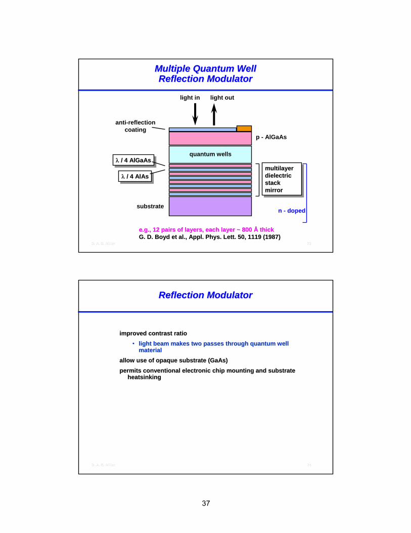
e.g., 12 pairs of layers, each layer ~ 800 e.g., 12 pairs of layers, each layer ~ 800 ÅÅ thickthickG. D. Boyd et al., Appl. Phys. Lett. 50, 1119 (1987)G. D. Boyd et al., Appl. Phys. Lett. 50, 1119 (1987)
7474D. A. B. MillerD. A. B. Miller
Reflection ModulatorReflection Modulator
improved contrast ratio improved contrast ratio •• light beam makes two passes through quantum well light beam makes two passes through quantum well
materialmaterialallow use of opaque substrate (GaAs)allow use of opaque substrate (GaAs)permits conventional electronic chip mounting and substrate permits conventional electronic chip mounting and substrate
heatsinkingheatsinking
38
7575D. A. B. MillerD. A. B. Miller
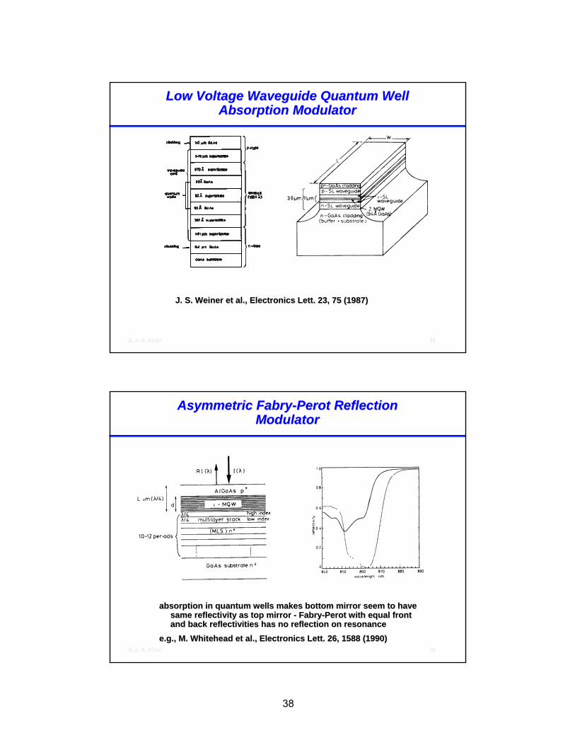
Low Voltage Waveguide Quantum Well Low Voltage Waveguide Quantum Well Absorption Modulator Absorption Modulator
J. S. Weiner et al., Electronics Lett. 23, 75 (1987)J. S. Weiner et al., Electronics Lett. 23, 75 (1987)
7676D. A. B. MillerD. A. B. Miller
Asymmetric FabryAsymmetric Fabry--Perot Reflection Perot Reflection ModulatorModulator
absorption in quantum wells makes bottom mirror seem to have absorption in quantum wells makes bottom mirror seem to have same reflectivity as top mirror same reflectivity as top mirror -- FabryFabry--Perot with equal front Perot with equal front and back reflectivities has no reflection on resonanceand back reflectivities has no reflection on resonance
e.g., M. Whitehead et al., Electronics Lett. 26, 1588 (1990)e.g., M. Whitehead et al., Electronics Lett. 26, 1588 (1990)

39
7777D. A. B. MillerD. A. B. Miller
Some Quantum Well ModulatorSome Quantum Well ModulatorMaterials SystemsMaterials Systems
MaterialMaterial Typical WavelengthTypical WavelengthGaAs/GaAlAsGaAs/GaAlAs 850 nm850 nm
InGaAs/InPInGaAs/InP 1.51.5 μμmmGaSb/GaAlSbGaSb/GaAlSb 1.51.5 μμmmInGaAs/GaAsInGaAs/GaAs 1.06 1.06 μμmmInAsP/InPInAsP/InP 1.06 1.06 μμmmAlGaAs/AlAsAlGaAs/AlAs 680 nm680 nm
InGaAsP/InPInGaAsP/InP 1.3 1.3 μμmmCdZnTe/ZnTeCdZnTe/ZnTe 610 nm610 nm
Ge/SiGeGe/SiGe 1.51.5 μμmm
GaAs/GaAlAs generally has the best physical performance GaAs/GaAlAs generally has the best physical performance because of its strong and sharp exciton linesbecause of its strong and sharp exciton lines
Recent work in Ge/SiGe is showing particularly clear Recent work in Ge/SiGe is showing particularly clear exciton lines at the longer wavelengthsexciton lines at the longer wavelengths
7878D. A. B. MillerD. A. B. Miller
Quantum Well Refraction ModulatorsQuantum Well Refraction Modulators
Material criterion for most refractive devices (including those Material criterion for most refractive devices (including those with resonators)with resonators)
•• change in optical path length in an absorption length must change in optical path length in an absorption length must be greater than half a wavelengthbe greater than half a wavelength
For quantum wells, must operate significantly away from For quantum wells, must operate significantly away from excitonic peaks to achieve this (move to low absorption).excitonic peaks to achieve this (move to low absorption).
Hence need about 500 microns length to make good device.Hence need about 500 microns length to make good device.Still better than most other electrorefractions.Still better than most other electrorefractions.
See, e.g., J. S. Weiner et al., Appl. Phys. Lett. 50, 842 (1987)See, e.g., J. S. Weiner et al., Appl. Phys. Lett. 50, 842 (1987)

40
7979D. A. B. MillerD. A. B. Miller
Quantum Well Absorption ModulatorsQuantum Well Absorption Modulators-- Features Features
voltages compatible with electronicsvoltages compatible with electronicssmall sizesmall sizelow energy low energy low chirplow chirphigh speed (40 GHz demonstrated)high speed (40 GHz demonstrated)
integration with electronicsintegration with electronics•• hybrid (solder bonding)hybrid (solder bonding)•• possible monolithic (Ge quantum wells on silicon)possible monolithic (Ge quantum wells on silicon)
significant modulation possible perpendicular to surface, significant modulation possible perpendicular to surface, allowing twoallowing two--dimensional arrays of devicesdimensional arrays of devices
apparently very reliableapparently very reliablevery high yields (e.g., < 1 in 1000 nonvery high yields (e.g., < 1 in 1000 non--working devices)working devices)
8080D. A. B. MillerD. A. B. Miller
Integrated Laser/ModulatorIntegrated Laser/Modulator
Uses quantum wells both for the laser gain region and for the Uses quantum wells both for the laser gain region and for the electroabsorption modulatorelectroabsorption modulator
Reduces Reduces ““chirpchirp”” compared to direct modulation of the lasercompared to direct modulation of the laserExtensively used for 2.5 Gb/s and 10 Gb/s fiber communicationsExtensively used for 2.5 Gb/s and 10 Gb/s fiber communications(A. Ramdane et al., IEEE J. Sel. Top. Quantum Electron. 2, 326 ((A. Ramdane et al., IEEE J. Sel. Top. Quantum Electron. 2, 326 (1996))1996))

41
8181D. A. B. MillerD. A. B. Miller
LongLong--wavelength optical modulator for highwavelength optical modulator for high--speed, speed, lowlow--power, lowpower, low--voltage, for array integration with voltage, for array integration with
CMOSCMOS
To connect optical networks directly to To connect optical networks directly to silicon CMOS, silicon CMOS,
•• need optical output device withneed optical output device with–– ~ 1 V drive~ 1 V drive–– Easy to alignEasy to align–– Array fabricationArray fabrication–– Telecommunications Telecommunications
wavelengths (1.5 microns)wavelengths (1.5 microns)–– Potentially high speedPotentially high speed
ProblemProblem•• Existing devices need waveguides Existing devices need waveguides
with very precise alignmentwith very precise alignmentSolutionSolution
•• Avoid waveguideAvoid waveguide–– Use shallow angle for long Use shallow angle for long
interaction length, and interaction length, and weak cavityweak cavity
–– Use 3 bounce optical Use 3 bounce optical design for positional design for positional alignment tolerancealignment tolerance
PerformancePerformance•• 1 V drive, 10 nm bandwidth, 30 1 V drive, 10 nm bandwidth, 30
microns alignment tolerance, array microns alignment tolerance, array fabricationfabrication N. C. Helman, J. E. Roth, D. P. Bour, H. Altug, and D. A. B. Miller, “Misalignment-
Tolerant Surface-Normal Low-Voltage Modulator for Optical Interconnects,” IEEE J. Selected Topics in Quantum Electronics, 11, 338 – 342 (2005)
Contrast ratio vs. wavelength for 1 V driveTolerance to misalignment
1480 1500 1520 1540 1560 15800.0
0.5
1.0
1.5
2.0
2.5
3.0
3.5
1 V drive:0.35 V to -0.65 V
Con
trast
Rat
io (d
B)
Wavelength (nm)
-60 -40 -20 0 20 40 60
0.0
0.2
0.4
0.6
0.8
1.0
30 μm
Nor
mal
ized
Ref
lect
ivity
(a.u
.)
Displacement along x-axis (μm)
Input – output relative alignment insensitive to position of device
Input Output
8282D. A. B. MillerD. A. B. Miller
Self Electrooptic Effect DeviceSelf Electrooptic Effect Device(SEED) Principle(SEED) Principle
CombineCombine•• quantum well modulatorquantum well modulator
withwith•• photodetectorphotodetector
to maketo make•• optically controlled device with optical outputoptically controlled device with optical output
Optical Optical -- electronic electronic -- optical conversion is efficient if device is optical conversion is efficient if device is integratedintegrated
D. A. B. Miller et al., IEEE J. Quantum Electron., QED. A. B. Miller et al., IEEE J. Quantum Electron., QE--21, 1462 21, 1462 (1985); "Quantum(1985); "Quantum--well selfwell self--electrooptic effect devices", D. A. electrooptic effect devices", D. A. B. Miller, Optical and Quantum Electron. 22 ,S61 (1990)B. Miller, Optical and Quantum Electron. 22 ,S61 (1990)

42
8383D. A. B. MillerD. A. B. Miller
Optically Controlled Optical GateOptically Controlled Optical Gate
BraggMirror
p
n
300μm
1μm
i
p+
ni
Signal
Control
0.1μm
Quantum WellStack
Top “Control”Diode
Bottom “Modulator”Diode
0 10 20 30 40 500.0
0.2
0.4
0.6
0.8
1.0
1.2
Data Theory
Ref
lect
ivity
Cha
nge
(a.u
.)
Time (ps)
Control short pulse in top diode generates carriersControl short pulse in top diode generates carriers•• Carriers move vertically, screening voltage locally in top diodeCarriers move vertically, screening voltage locally in top diode
–– changing voltage locally in bottom diodechanging voltage locally in bottom diode
•• changing absorption in bottom diode (and hence reflectivity)changing absorption in bottom diode (and hence reflectivity)Voltage changes relax rapidly by local conduction within structuVoltage changes relax rapidly by local conduction within structure re Candidate for a wavelength converter for optical networksCandidate for a wavelength converter for optical networksM. B. Yairi, C. W. Coldren, D. A. B. Miller, and J. S. Harris, Jr., Appl. Phys. Lett. 75
(5), 597-599 (1999)
8484D. A. B. MillerD. A. B. Miller
cw beam 1
cw beam 2
@λΟ1
@λΟ2
output 1@λΟ1
output 2@λΟ2
input 1 @λΙ1 input 2 @λΙ2
λΙ1 → λΟ2
λΙ2 → λΟ1
1mm
0.6mm
-+ Von
+Von
-+ Von
+Von
-+ Voff
+Voff
-+ Voff
+Voff
2x2 array
@λiinput data
cw beam output data
quantum well modulator
photodiode
@λo @λo
50 µm
Fabricated Wavelength Converting CrossbarsFabricated Wavelength Converting Crossbars
Integrate quantum well modulator directly driven by Integrate quantum well modulator directly driven by photodetectorphotodetector
•• Allows wavelength conversionAllows wavelength conversion–– Including crossbar operationIncluding crossbar operation
•• Allows rapid electrical reconfigurationAllows rapid electrical reconfigurationDemonstrated Demonstrated
• C-band λ-conversion: 1530-1565 nm (PD input) to 1530-1565 nm (EAM output) with 1 GHz 3-dB bandwidth
•• 2.5 Gb/s conversion 2.5 Gb/s conversion H. V. Demir, V. A. Sabnis, O. Fidaner, J.-F. Zheng, J. S. Harris, Jr., D. A. B. Miller, “Multifunctional integrated photonic switches,” IEEE J. Selected Topics in Quantum
Electronics 11, No. 1, 86 – 98 (2005)
43
8585D. A. B. MillerD. A. B. Miller
solder (1000 Å)n +
silicon
GaAsp AlGaAs
epoxy
i MQW
silicon
epoxy
silicon
anti-reflectioncoating
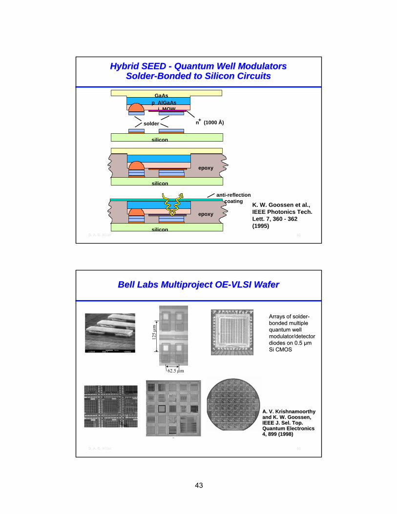
Hybrid SEED Hybrid SEED -- Quantum Well Modulators Quantum Well Modulators SolderSolder--Bonded to Silicon CircuitsBonded to Silicon Circuits
K. W. Goossen et al., IEEE Photonics Tech. Lett. 7, 360 - 362 (1995)
8686D. A. B. MillerD. A. B. Miller
Bell Labs Multiproject OEBell Labs Multiproject OE--VLSI WaferVLSI Wafer
A. V. Krishnamoorthy A. V. Krishnamoorthy and K. W. Goossen, and K. W. Goossen, IEEE J. Sel. Top. IEEE J. Sel. Top. Quantum Electronics Quantum Electronics 4, 899 (1998) 4, 899 (1998)
Arrays of solderArrays of solder--bonded multiple bonded multiple quantum well quantum well modulator/detector modulator/detector diodes on 0.5 diodes on 0.5 µµm m Si CMOSSi CMOS
62.5 μm
125
μm
44
8787D. A. B. MillerD. A. B. Miller
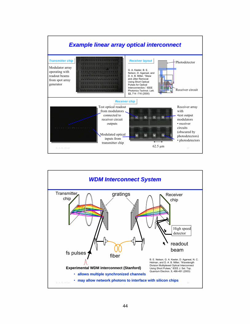
Example linear array optical interconnectExample linear array optical interconnect
Transmitter chipTransmitter chip
Receiver array with •test output modulators• receiver circuits (obscured by photodetectors)• photodetectors
Test optical readout from modulators
connected to receiver circuit
outputs
Modulated optical inputs from
transmitter chip
Photodetector
Receiver circuit
62.5 µm
Receiver chipReceiver chip
Modulator array operating with readout beams from spot array generator
Receiver layoutReceiver layout
G. A. Keeler, B. E. Nelson, D. Agarwal, and D. A. B. Miller, “Skew and Jitter Removal Using Short Optical Pulses for Optical Interconnection,” IEEE Photonics Technol. Lett. 12, 714 -716 (2000)
8888D. A. B. MillerD. A. B. Miller
WDM Interconnect SystemWDM Interconnect System
Experimental WDM interconnect (Stanford)Experimental WDM interconnect (Stanford)•• allows multiple synchronized channelsallows multiple synchronized channels
•• may allow network photons to interface with silicon chipsmay allow network photons to interface with silicon chips
gratings
fiber
Receiverchip
Transmitterchip
readout beamfs pulses
High speeddetector
B. E. Nelson, G. A. Keeler, D. Agarwal, N. C. Helman, and D. A. B. Miller, “Wavelength Division Multiplexed Optical Interconnect Using Short Pulses,” IEEE J. Sel. Top. Quantum Electron. 9, 486-491 (2003)

45
8989D. A. B. MillerD. A. B. Miller
Wavelength division multiplexing to Si Wavelength division multiplexing to Si CMOSCMOS
For distances beyond 10For distances beyond 10’’s of cm, must use s of cm, must use fiber for optical interconnectsfiber for optical interconnects
For large systems, one 10 For large systems, one 10 –– 40 Gb/s channel 40 Gb/s channel per fiber may mean too many fibersper fiber may mean too many fibers
Would also like to be able to use the same Would also like to be able to use the same physical technology for interconnect and physical technology for interconnect and for connecting to longer distance optical for connecting to longer distance optical networksnetworks
•• Note Si CMOS speeds of 10 GHz Note Si CMOS speeds of 10 GHz and above allow entire fiber and above allow entire fiber bandwidth to be filled by WDM bandwidth to be filled by WDM (wavelength division multiplexing)(wavelength division multiplexing)
•• Use of same technology for both Use of same technology for both purposes increases market, reduces purposes increases market, reduces costcost
–– Convergence of networking and Convergence of networking and silicon industries?silicon industries?
Solution Solution –– interface WDM optical fiber directly interface WDM optical fiber directly to silicon? to silicon?
•• WDM splitters/combinersWDM splitters/combiners•• Modulator and detector arrays Modulator and detector arrays
hybridized or integrated onto hybridized or integrated onto silicon?silicon?
CMOS chip
Output WDM fiber
Input WDM fiberOptical power
from multiwavelength
source
WDM splitter
WDM combinerModulator
array
Detector array
9090D. A. B. MillerD. A. B. Miller
Germanium Quantum Well Physics and Germanium Quantum Well Physics and DevicesDevices
Ge, Si, and SiGe properties Ge, Si, and SiGe properties •• Direct and indirect band gapsDirect and indirect band gaps•• Ge and Si optical absorptionGe and Si optical absorption•• Strain and band structureStrain and band structure
Ge quantum wells and electroabsorptionGe quantum wells and electroabsorption•• Growth of Ge on SiGeGrowth of Ge on SiGe
•• Band structures for Ge quantum wellsBand structures for Ge quantum wells•• Ge quantum well QCSE electroabsorptionGe quantum well QCSE electroabsorption•• Comparison with IIIComparison with III--V QCSE V QCSE
Device prospectsDevice prospects•• Length scales and possible configurationsLength scales and possible configurations
Y.-H. Kuo, Y.-K. Lee, Y. Ge, S. Ren, J. E. Roth, T. I. Kamins, D. A. B. Miller & J. S. Harris, “Strong quantum-confined Stark effect in germanium quantum-well structures on silicon,” Nature 437, 1334-1336 (2005) (27 October 2005|doi:10.1038/nature04204)Y.-H. Kuo, Y. K. Lee, Y. Ge, S. Ren, J. E. Roth, T. I. Kamins, D. A. B. Miller, and J. S. Harris, “Quantum-Confined Stark Effect in Ge/SiGe Quantum Wells on Si for Optical Modulators ,” IEEE J. Sel. Top. Quantum Electron. 12, 1503-1513 (2006)

46
9191D. A. B. MillerD. A. B. Miller
Direct and Indirect Band GapsDirect and Indirect Band Gaps
Electrons and holes settle to points of the Electrons and holes settle to points of the samesame momentum momentum Strong emission and absorption across Strong emission and absorption across direct gapdirect gap
•• no momentum change requiredno momentum change required
Electrons and holes settle to points of Electrons and holes settle to points of differentdifferent momentummomentumWeak emission and absorption across the Weak emission and absorption across the indirect gapindirect gap
•• photon has negligible momentum, photon has negligible momentum, so phonon also required so phonon also required
Electron energy
Momentum (k) Momentum (k)
Global conduction
band minimum above valence band maximum
Electron energy
Global conduction band
minimum notabove valence band maximum
DirectDirect IndirectIndirect
Note that both can have strong absorption across the direct gapNote that both can have strong absorption across the direct gap
Direct band gapIndirect band gap
9292D. A. B. MillerD. A. B. Miller
Ge and Si Band StructuresGe and Si Band Structures
Both indirect band gap materialsBoth indirect band gap materialsGe also has a direct gap at ~ 1550 nmGe also has a direct gap at ~ 1550 nm
•• Physics of this direct gap essentially similar to that of, Physics of this direct gap essentially similar to that of, e.g., GaAse.g., GaAs
Corresponding direct gap in Si at ~ 300 nmCorresponding direct gap in Si at ~ 300 nmExpect GeExpect Ge--rich SiGe band structure to be like Ge, but ~ linearly rich SiGe band structure to be like Ge, but ~ linearly
interpolate band gaps and masses towards Si band interpolate band gaps and masses towards Si band structure (structure (Kuo et al. 2006Kuo et al. 2006))
Ge Si
k
4.175 eV (~ 300 nm)
HH
LH
[111] [100]
L1
L32′Γ
Δ
k
L
[100][111]
Γ
HH
LH
0.8 eV (1550nm)
[100] – “z” cube edge direction[111] – cubic space diagonal directionΓ − “zone-center” (k=0) pointL – “zone-edge” point in [111] directionΔ – specific point in [100] direction with
minimum energy in Si conduction bandLH – “light hole” valence bandHH – “heavy hole” valence bandL1, L3, Γ2′ – specific Si conduction bands

47
9393D. A. B. MillerD. A. B. Miller
Ge and Si Optical AbsorptionGe and Si Optical Absorption
GaAs GaAs –– classic classic ““direct gapdirect gap”” semiconductorsemiconductor
•• Strong absorption edge when Strong absorption edge when photon energy equals bandgap photon energy equals bandgap energyenergy
Si Si –– classic classic ““indirect gapindirect gap”” semiconductorsemiconductor•• Weak Weak ““phononphonon--assistedassisted”” absorption absorption
tail extending past 1 microntail extending past 1 micronGe Ge –– also indirect, with phononalso indirect, with phonon--assisted assisted
absorption tailabsorption tail•• But also strong direct gap But also strong direct gap
absorption edge at ~ 1550 nmabsorption edge at ~ 1550 nm
figure after A. Nemecek, G. Zach, S. Swoboda, K. Oberhauser, and H. Zimmermann, “Integrated BiCMOS p-i-n Photodetectors With High Bandwidth and High Responsivity,” IEEE J. Sel. Top. Quantum Electron. 12, 1469-1475 (2006)
Si
GaAsGe
0.2 0.6 1.0 1.4 1.80.4 0.8 1.2 1.6
104
103
102
101
105
106
Wavelength (microns)
Abs
orpt
ion
coef
ficie
nt (c
m-1
)
9494D. A. B. MillerD. A. B. Miller
Strained Band StructuresStrained Band Structures
Growing Ge on Si, or on some SiGe alloy, involves strainGrowing Ge on Si, or on some SiGe alloy, involves strain•• Ge lattice spacing ~ 4% larger than that of SiGe lattice spacing ~ 4% larger than that of Si
–– so Ge is under biaxial compressive strainso Ge is under biaxial compressive strain
Compressivelystrained Ge well
Tensile-strained Ge-rich SiGe barrier
k
L
HH
LH
[100]
Γ
k
LHH
LH[100][111]
Γ
Unstrained Ge
k
L
[100][111]
Γ
HH
LH
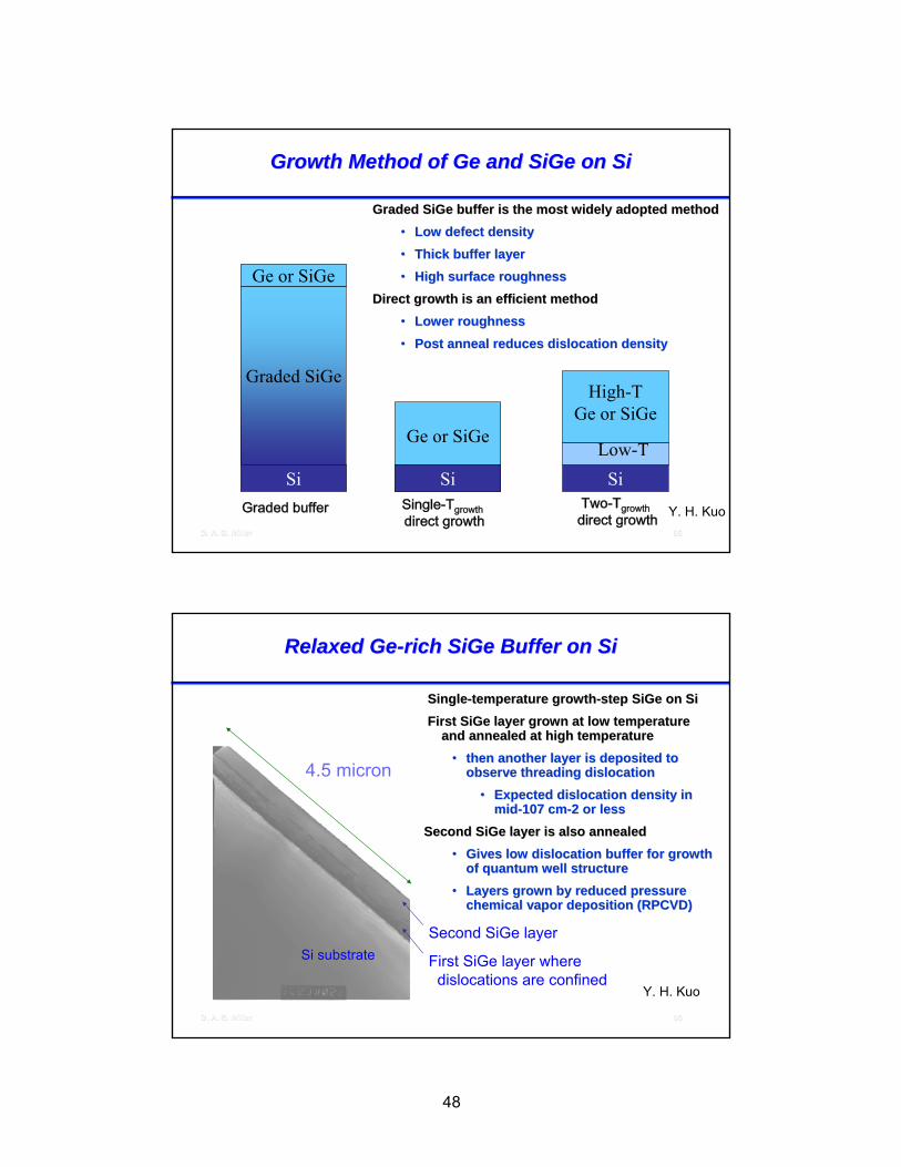
48
9595D. A. B. MillerD. A. B. Miller
Growth Method of Ge and SiGe on SiGrowth Method of Ge and SiGe on Si
Graded SiGe buffer is the most widely adopted methodGraded SiGe buffer is the most widely adopted method•• Low defect densityLow defect density•• Thick buffer layer Thick buffer layer •• High surface roughnessHigh surface roughness
Direct growth is an efficient methodDirect growth is an efficient method•• Lower roughnessLower roughness
•• Post anneal reduces dislocation densityPost anneal reduces dislocation density
Si
Graded SiGe
Ge or SiGe
Ge or SiGe
Si SiLow-T
High-TGe or SiGe
Graded buffer Single-Tgrowthdirect growth
Two-Tgrowthdirect growth Y. H. Kuo
9696D. A. B. MillerD. A. B. Miller
Relaxed GeRelaxed Ge--rich SiGe Buffer on Sirich SiGe Buffer on Si
4.5 micron
SingleSingle--temperature growthtemperature growth--step SiGe on Si step SiGe on Si First SiGe layer grown at low temperature First SiGe layer grown at low temperature
and annealed at high temperature and annealed at high temperature •• then another layer is deposited to then another layer is deposited to
observe threading dislocationobserve threading dislocation•• Expected dislocation density in Expected dislocation density in
midmid--107 cm107 cm--2 or less2 or lessSecond SiGe layer is also annealedSecond SiGe layer is also annealed
•• Gives low dislocation buffer for growth Gives low dislocation buffer for growth of quantum well structureof quantum well structure
•• Layers grown by reduced pressure Layers grown by reduced pressure chemical vapor deposition (RPCVD)chemical vapor deposition (RPCVD)
Si substrate First SiGe layer where dislocations are confined
Second SiGe layer
Y. H. Kuo

49
9797D. A. B. MillerD. A. B. Miller
Strained Ge/SiGe Multiple Quantum WellsStrained Ge/SiGe Multiple Quantum Wells
Regular and sharp MQW structureRegular and sharp MQW structure
10nm Ge well 10nm Ge well 16nm SiGe barrier16nm SiGe barrier
Y. H. Kuo
9898D. A. B. MillerD. A. B. Miller
StrainStrain--Balanced StructureBalanced Structure
n+ SiGe cap layer
Silicon Substrate
p+ Relaxed SiGe buffer layer
Undoped SiGe buffer layer
Undoped SiGe buffer layer
Strain force ε
Average Si concentration in Ge/SiGe Average Si concentration in Ge/SiGe quantum wells equals that in SiGe quantum wells equals that in SiGe bufferbuffer
•• Allows growth of thick structures Allows growth of thick structures without exceeding critical without exceeding critical thickness for strained growththickness for strained growth
Compressive
growth direction
Tensile
Ge/SiGe quantum wells
Y. H. Kuo
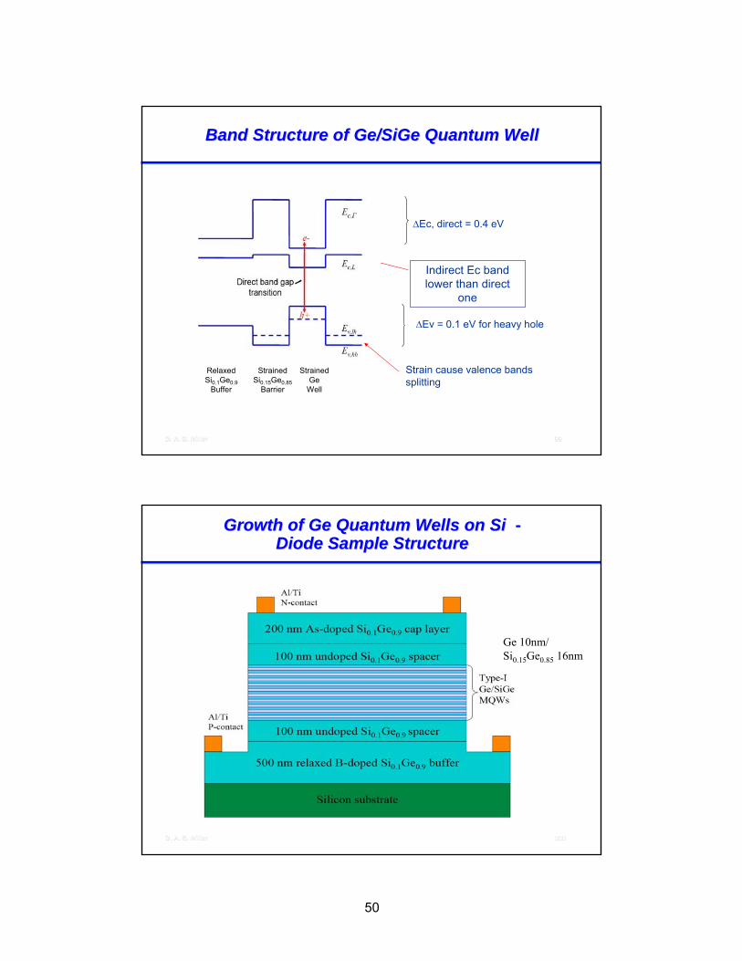
50
9999D. A. B. MillerD. A. B. Miller
Band Structure of Ge/SiGe Quantum WellBand Structure of Ge/SiGe Quantum Well
∆Ec, direct = 0.4 eV
∆Ev = 0.1 eV for heavy hole
Strain cause valence bands splitting
Indirect Ec band lower than direct
one
RelaxedSi0.1Ge0.9
Buffer
StrainedSi0.15Ge0.85
Barrier
StrainedGe
Well
100100D. A. B. MillerD. A. B. Miller
Ge 10nm/Si0.15Ge0.85 16nm
Growth of Ge Quantum Wells on Si Growth of Ge Quantum Wells on Si --Diode Sample StructureDiode Sample Structure
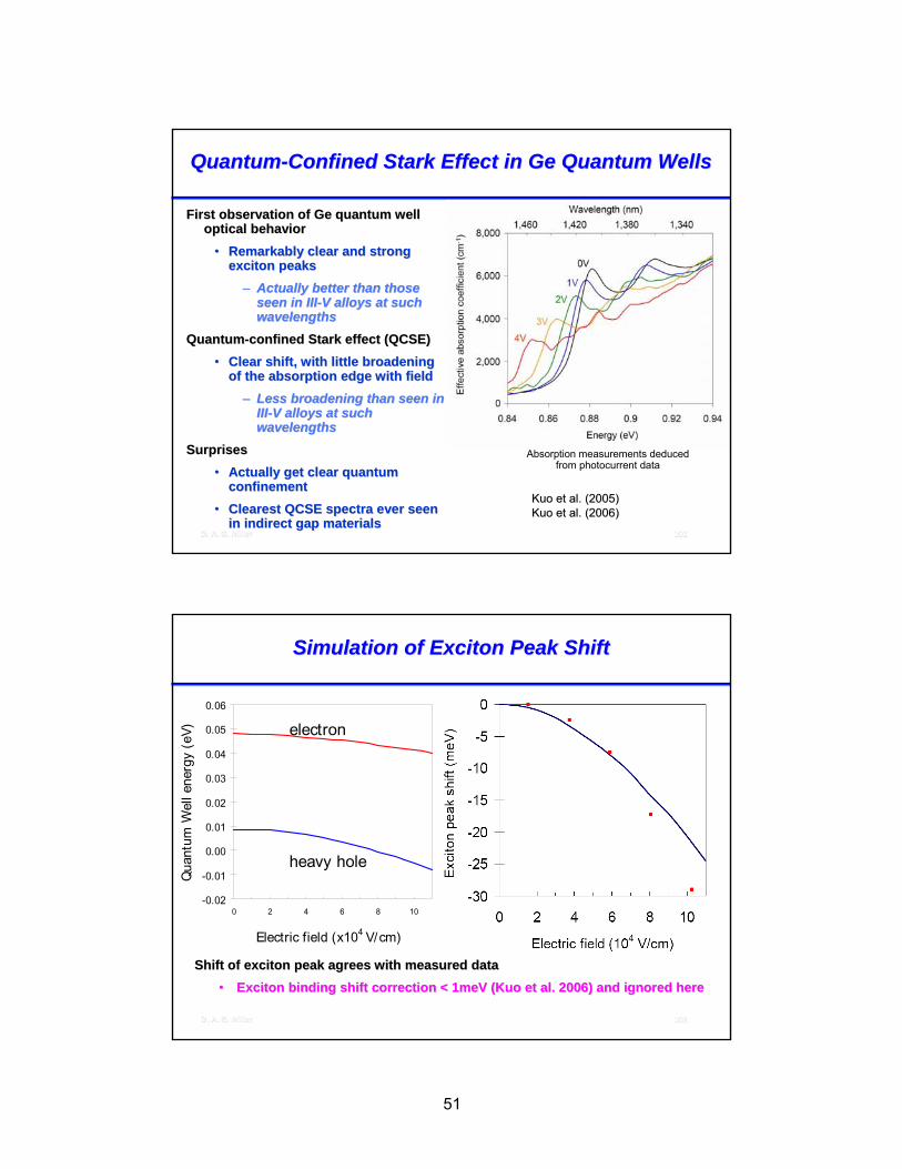
51
101101D. A. B. MillerD. A. B. Miller
QuantumQuantum--Confined Stark Effect in Ge Quantum WellsConfined Stark Effect in Ge Quantum Wells
First observation of Ge quantum well First observation of Ge quantum well optical behavioroptical behavior
•• Remarkably clear and strong Remarkably clear and strong exciton peaksexciton peaks
–– Actually better than those Actually better than those seen in IIIseen in III--V alloys at such V alloys at such wavelengths wavelengths
QuantumQuantum--confined Stark effect (QCSE)confined Stark effect (QCSE)•• Clear shift, with little broadening Clear shift, with little broadening
of the absorption edge with fieldof the absorption edge with field–– Less broadening than seen in Less broadening than seen in
IIIIII--V alloys at such V alloys at such wavelengthswavelengths
SurprisesSurprises•• Actually get clear quantum Actually get clear quantum
confinementconfinement•• Clearest QCSE spectra ever seen Clearest QCSE spectra ever seen
in indirect gap materialsin indirect gap materials
Kuo et al.Kuo et al. (2005)(2005)Kuo et al.Kuo et al. (2006)(2006)
Absorption measurements deduced from photocurrent data
102102D. A. B. MillerD. A. B. Miller
Simulation of Exciton Peak ShiftSimulation of Exciton Peak Shift
Shift of exciton peak agrees with measured dataShift of exciton peak agrees with measured data•• Exciton binding shift correction < 1meV (Kuo et al. 2006) and iExciton binding shift correction < 1meV (Kuo et al. 2006) and ignored heregnored here
-0.02
-0.01
0.00
0.01
0.02
0.03
0.04
0.05
0.06
0 2 4 6 8 10
Electric field (x104 V/cm)
Quan
tum
Wel
l ene
rgy
(eV) electron
heavy hole
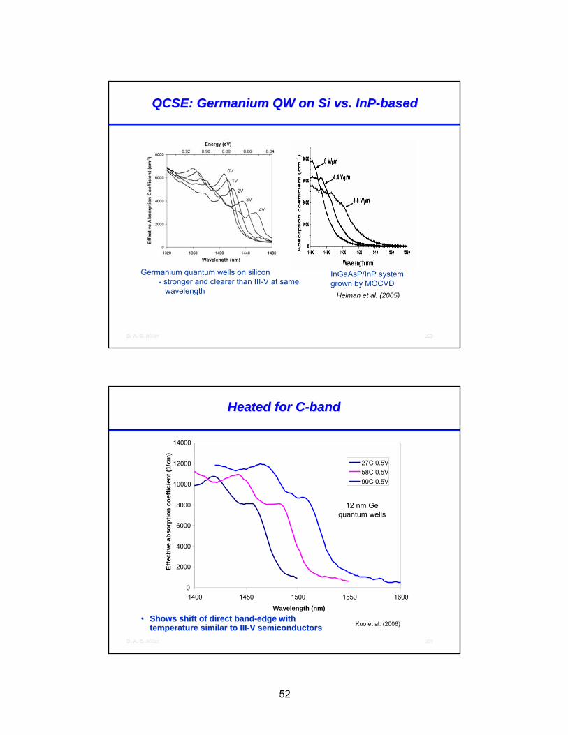
52
103103D. A. B. MillerD. A. B. Miller
QCSE: Germanium QW on Si vs. InPQCSE: Germanium QW on Si vs. InP--basedbased
InGaAsP/InP system grown by MOCVD
Helman et al. (2005)
Germanium quantum wells on silicon - stronger and clearer than III-V at same
wavelength
104104D. A. B. MillerD. A. B. Miller
Heated for CHeated for C--bandband
Kuo et al. (2006)
0
2000
4000
6000
8000
1400 1450 1500 1550 1600
Wavelength (nm)
27C 0.5V58C 0.5V90C 0.5V10000
12000
14000
Effe
ctiv
e ab
sorp
tion
coef
ficie
nt (1
/cm
)
•• Shows shift of direct bandShows shift of direct band--edge with edge with temperature similar to IIItemperature similar to III--V semiconductorsV semiconductors
12 nm Ge quantum wells

53
105105D. A. B. MillerD. A. B. Miller
Operation in the Telecommunications COperation in the Telecommunications C--bandband
Shift the operation to the CShift the operation to the C--band (~ 1530 band (~ 1530 –– 1565 nm) 1565 nm) by by
•• Redesign of quantum Redesign of quantum well (thicker well (thicker –– 12 nm, 12 nm, less strain)less strain)
•• Heating to the Heating to the operating operating temperature of a temperature of a typical silicon chip (~ typical silicon chip (~ 90C)90C)
0
2000
4000
6000
8000
10000
12000
14000
1400 1450 1500 1550 1600
Wavelength (nm)
Effe
ctiv
e ab
sorp
tion
coef
ficie
nt (1
/cm
) 90C 0V90C 0.5V90C 1V90C 1.5V90C 2V
Kuo et al. (2006)
106106D. A. B. MillerD. A. B. Miller
Device ProspectsDevice Prospects
Differences compared to IIIDifferences compared to III--V technologyV technology•• Ge already process compatible with Si Ge already process compatible with Si •• refractive indices of Ge (~ 4.2) and Si (~ 3.5) quite differentrefractive indices of Ge (~ 4.2) and Si (~ 3.5) quite different•• some background absorption from indirect absorption tailsome background absorption from indirect absorption tail•• dondon’’t have lattice matched materials of controllable index t have lattice matched materials of controllable index
–– cannot take quite the same kind of waveguide cannot take quite the same kind of waveguide approach as in IIIapproach as in III--VV’’ss
•• do have several material options with large index contrast, do have several material options with large index contrast, including including
–– silicon dioxidesilicon dioxide–– Ge and Si themselves (large index difference)Ge and Si themselves (large index difference)

54
107107D. A. B. MillerD. A. B. Miller
Device Length ScalesDevice Length Scales
Effect is so large that resonators are not essential Effect is so large that resonators are not essential •• Could make short Could make short ““singlesingle--passpass”” devices devices
E.g., absorption coefficient change of 3000 cmE.g., absorption coefficient change of 3000 cm--11 over a over a background absorption of 1000 cmbackground absorption of 1000 cm--11 would give would give
•• 3 dB contrast and 1 dB absorption loss in a device 2.3 3 dB contrast and 1 dB absorption loss in a device 2.3 microns long microns long
•• 10 dB contrast and 3.3 dB absorption loss in a device 7.7 10 dB contrast and 3.3 dB absorption loss in a device 7.7 microns longmicrons long
•• In a waveguide with fill factor In a waveguide with fill factor ΓΓ = 0.1, multiply lengths by = 0.1, multiply lengths by 1010
–– 3 dB contrast and 1 dB absorption loss in a device 23 3 dB contrast and 1 dB absorption loss in a device 23 microns longmicrons long
–– 10 dB contrast and 3.3 dB absorption loss in a device 10 dB contrast and 3.3 dB absorption loss in a device 77 microns long77 microns long
108108D. A. B. MillerD. A. B. Miller
Transmission Spectra and First Modulator Transmission Spectra and First Modulator ResultsResults
Very clean electroabsorption Very clean electroabsorption •• high uniformity in samples high uniformity in samples
with as many as 60 quantum with as many as 60 quantum wellswells
•• directly showing optical directly showing optical modulation of transmissionmodulation of transmission
•• clear measurable clear measurable transmission change with transmission change with voltage even in single pass voltage even in single pass through ~ 3 microns total through ~ 3 microns total thicknessthickness
first modulator now demonstratedfirst modulator now demonstrated•• withwith 7.3 dB contrast7.3 dB contrast•• misalignment tolerantmisalignment tolerant•• concept related to QWAFEMconcept related to QWAFEM
J. E. Roth, O. Fidaner, R. K. Schaevitz, Y.-H. Kuo, T. I. Kamins, J. S. Harris, and D. A. B. Miller (submitted to Optics Express)
Wavelength (nm)
Tran
smis
sion
1430 1440 1450 1460 1470 14800.5
0.55
0.6
0.65
0.7
0.75
0.8
0.85
0.9
0.95
Transmission spectra for different electric fields, 60 quantum well sample
0.4 x 10⁴ V/cm
11 x 104 V/cm

55
109109D. A. B. MillerD. A. B. Miller
General References General References --Quantum Well Optical Physics and DevicesQuantum Well Optical Physics and Devices
Extensive discussion of quantum well optical physics Extensive discussion of quantum well optical physics --
S. SchmittS. Schmitt--Rink, D. S. Chemla, and D. A. B. Miller, "Linear and nonlinear Rink, D. S. Chemla, and D. A. B. Miller, "Linear and nonlinear optical properties of semiconductor quantum wells", Advances in optical properties of semiconductor quantum wells", Advances in Physics 38, 89Physics 38, 89--188 (1989)188 (1989)
Band structure and states in quantum wells Band structure and states in quantum wells --
G. Bastard, "Wave mechanics applied to semiconductor heterostrucG. Bastard, "Wave mechanics applied to semiconductor heterostructures", tures", (Les Editions de Physique, Les Ulis, France)(Les Editions de Physique, Les Ulis, France)
110110D. A. B. MillerD. A. B. Miller
General References General References --Quantum Well Optical Physics and Quantum Well Optical Physics and
Devices and Optical SystemsDevices and Optical Systems
Summary treatment of quantum well optoelectronic devices Summary treatment of quantum well optoelectronic devices D. A. B. Miller, “Optics for Digital Information Processing,” in
Semiconductor Quantum Optoelectronics, Eds. A. Miller, M. Ebrahimzadeh, and D. M. Finlayson, Proceedings of the Fiftieth Scottish Universities Summer School in Physics, St. Andrews (June 1998). (Publishers: The Scottish Universities Summer School in Physics, SUSSP Publications, and Institute of Physics Publishing, 1999), pp 433-461
Use of optics for interconnectionUse of optics for interconnectionD. A. B. Miller, “Rationale and Challenges for Optical Interconnects to
Electronic Chips,” Proc. IEEE 88, 728-749 (2000)D. A. B. Miller, “Physical Reasons for Optical Interconnection,” Special
Issue on Smart Pixels, Int’l J. Optoelectronics 11 (3), 155-168 (1997)
See http://ee.stanford.edu/~dabm