random-access memory distributed and block ram discussion d10.3 example 41
Post on 22-Dec-2015
224 views
TRANSCRIPT
Random-Access MemoryDistributed and Block RAM
Discussion D10.3
Example 41
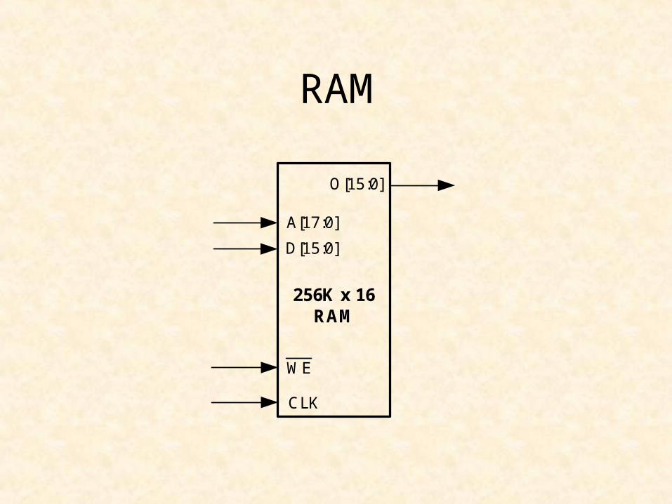
RAM
256K x 16RAM
A[17:0]
D[15:0]
WE
CLK
O[15:0]
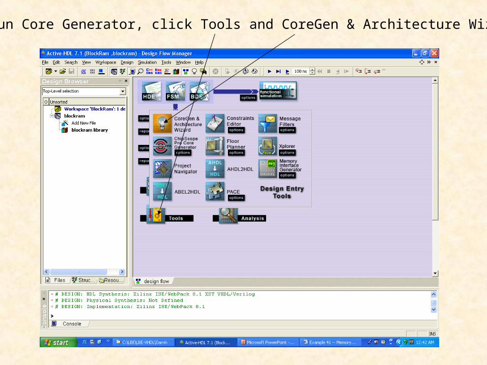
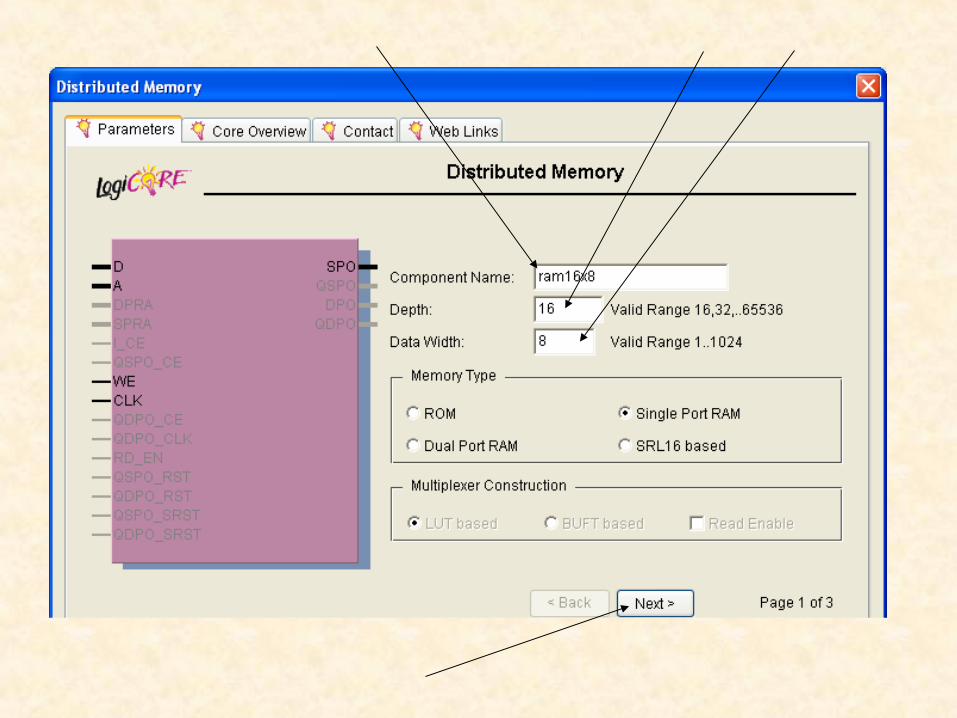
To run Core Generator, click Tools and CoreGen & Architecture Wizard

Then, select Memories & Storage Elements RAMs & ROMs Distributed Memory (ver 7.1)
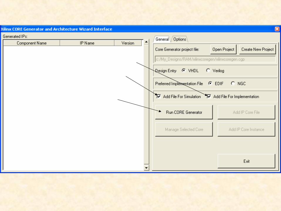
Select Project Options
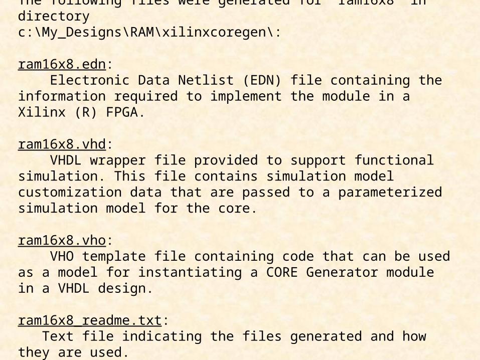
The following files were generated for 'ram16x8' in directory c:\My_Designs\RAM\xilinxcoregen\:
ram16x8.edn: Electronic Data Netlist (EDN) file containing the information required to implement the module in a Xilinx (R) FPGA.
ram16x8.vhd: VHDL wrapper file provided to support functional simulation. This file contains simulation model customization data that are passed to a parameterized simulation model for the core.
ram16x8.vho: VHO template file containing code that can be used as a model for instantiating a CORE Generator module in a VHDL design.
ram16x8_readme.txt: Text file indicating the files generated and how they are used.
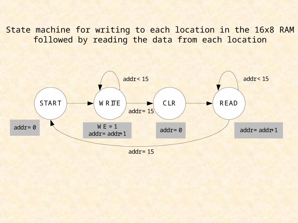
START WRITE CLR READ
addr < 15
addr = 15
addr < 15
addr = 15
WE = 1addr = addr+1
addr = addr+1addr = 0addr = 0
State machine for writing to each location in the 16x8 RAM followed by reading the data from each location
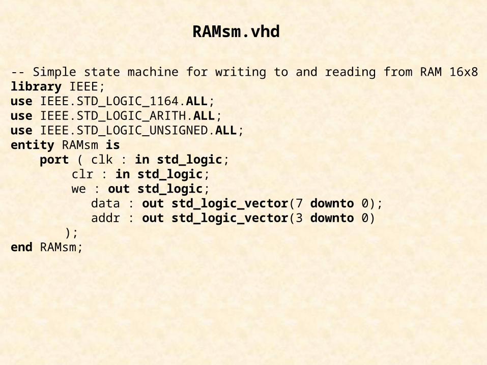
-- Simple state machine for writing to and reading from RAM 16x8library IEEE;use IEEE.STD_LOGIC_1164.ALL;use IEEE.STD_LOGIC_ARITH.ALL;use IEEE.STD_LOGIC_UNSIGNED.ALL;entity RAMsm is port ( clk : in std_logic;
clr : in std_logic; we : out std_logic;
data : out std_logic_vector(7 downto 0); addr : out std_logic_vector(3 downto 0)
);end RAMsm;
RAMsm.vhd
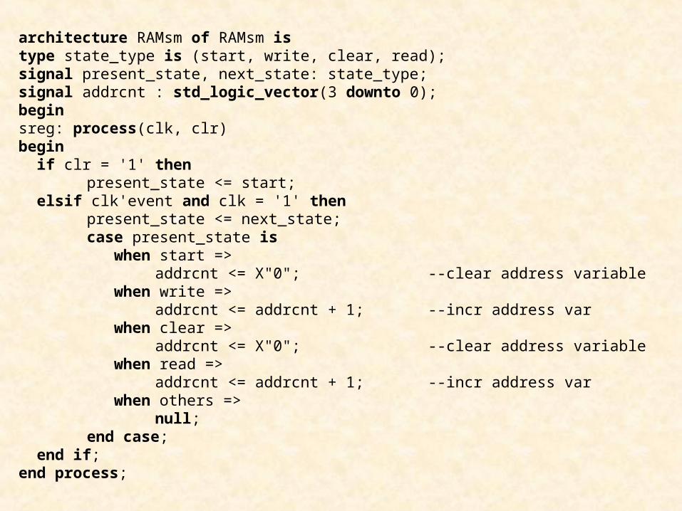
architecture RAMsm of RAMsm istype state_type is (start, write, clear, read);signal present_state, next_state: state_type;signal addrcnt : std_logic_vector(3 downto 0);beginsreg: process(clk, clr)begin if clr = '1' then present_state <= start; elsif clk'event and clk = '1' then
present_state <= next_state;case present_state is when start =>
addrcnt <= X"0"; --clear address variable when write =>
addrcnt <= addrcnt + 1; --incr address var when clear =>
addrcnt <= X"0"; --clear address variable when read =>
addrcnt <= addrcnt + 1; --incr address var when others =>
null; end case; end if; end process;

C1: process(present_state, addrcnt)begin case present_state is
when start => next_state <= write;when write => if addrcnt < 15 then next_state <= write; else next_state <= clear; end if; when clear => next_state <= read;when read => if addrcnt < 15 then next_state <= read; else next_state <= start; end if; when others => null;end case;
end process;
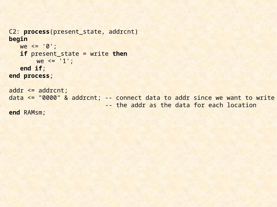
C2: process(present_state, addrcnt)begin we <= '0'; if present_state = write then
we <= '1'; end if;end process;
addr <= addrcnt;data <= "0000" & addrcnt; -- connect data to addr since we want to write
-- the addr as the data for each locationend RAMsm;
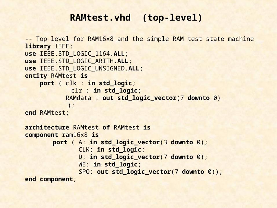
RAMtest.vhd (top-level)
-- Top level for RAM16x8 and the simple RAM test state machinelibrary IEEE;use IEEE.STD_LOGIC_1164.ALL;use IEEE.STD_LOGIC_ARITH.ALL;use IEEE.STD_LOGIC_UNSIGNED.ALL;entity RAMtest is port ( clk : in std_logic;
clr : in std_logic; RAMdata : out std_logic_vector(7 downto 0)
);end RAMtest;
architecture RAMtest of RAMtest iscomponent ram16x8 is
port ( A: in std_logic_vector(3 downto 0); CLK: in std_logic; D: in std_logic_vector(7 downto 0); WE: in std_logic; SPO: out std_logic_vector(7 downto 0));
end component;

component RAMsm is port ( clk : in std_logic;
clr : in std_logic; we : out std_logic;
data : out std_logic_vector(7 downto 0); addr : out std_logic_vector(3 downto 0));end component;
signal data : std_logic_vector(7 downto 0);signal addr : std_logic_vector(3 downto 0);signal we : std_logic;
begin
RAM: ram16x8 port map(A => addr, CLK => clk, D => data, WE => we, SPO => RAMdata);
SM: RAMsm port map(clk => clk, clr => clr, we => we, data => data, addr => addr);
end RAMtest;
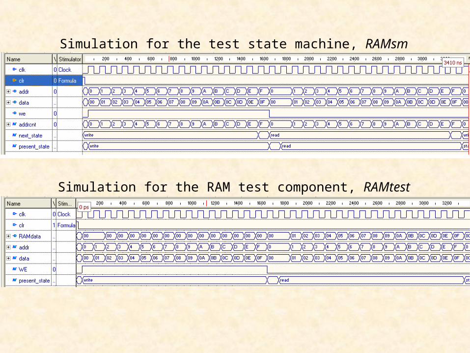
Simulation for the test state machine, RAMsm
Simulation for the RAM test component, RAMtest
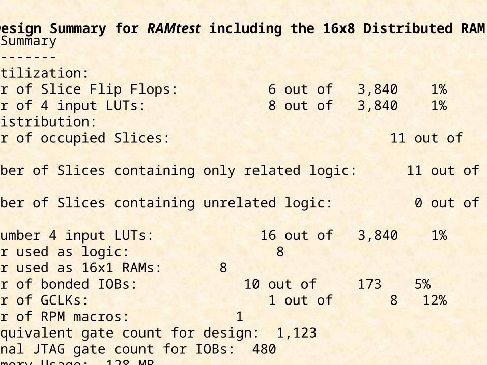
Design Summary--------------Logic Utilization: Number of Slice Flip Flops: 6 out of 3,840 1% Number of 4 input LUTs: 8 out of 3,840 1%Logic Distribution: Number of occupied Slices: 11 out of 1,920 1% Number of Slices containing only related logic: 11 out of 11
100% Number of Slices containing unrelated logic: 0 out of 11
0%Total Number 4 input LUTs: 16 out of 3,840 1% Number used as logic: 8 Number used as 16x1 RAMs: 8 Number of bonded IOBs: 10 out of 173 5% Number of GCLKs: 1 out of 8 12% Number of RPM macros: 1Total equivalent gate count for design: 1,123Additional JTAG gate count for IOBs: 480Peak Memory Usage: 128 MB
Design Summary for RAMtest including the 16x8 Distributed RAM
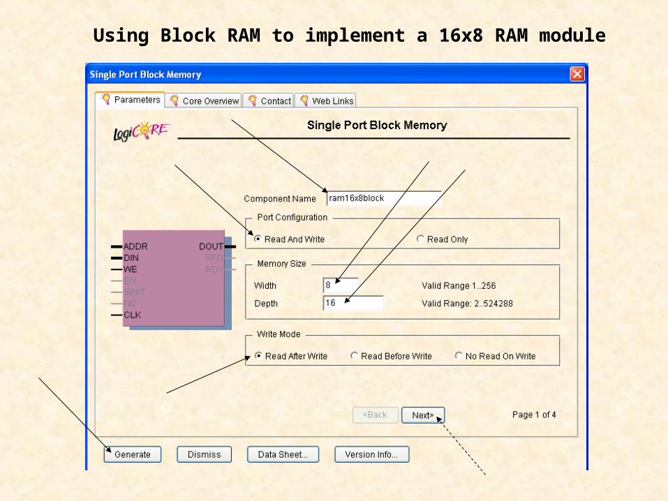
Using Block RAM to implement a 16x8 RAM module
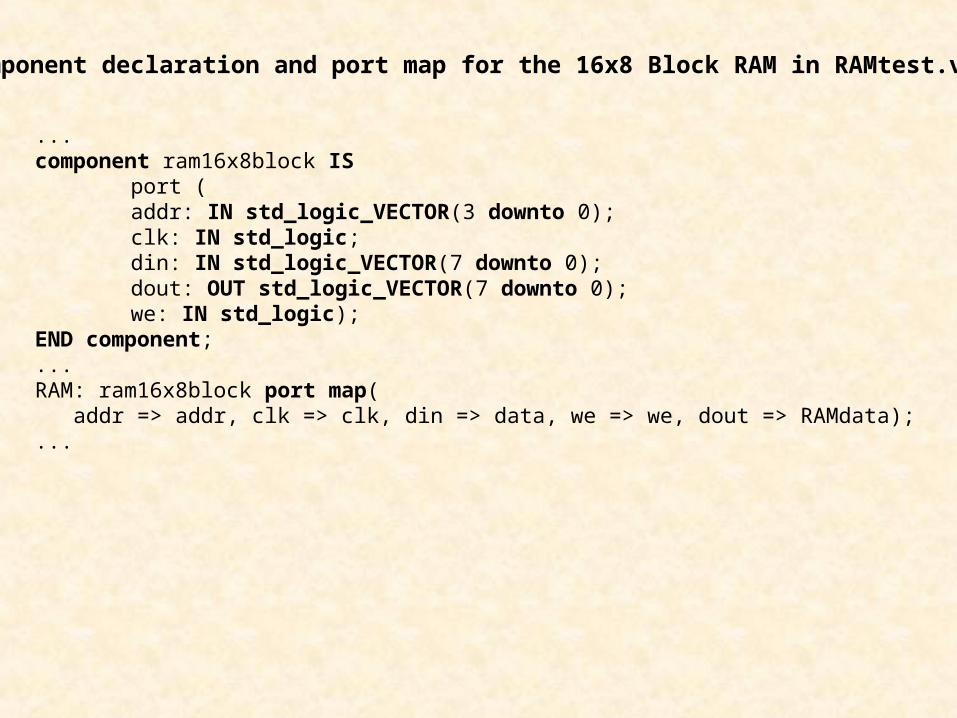
...component ram16x8block IS
port (addr: IN std_logic_VECTOR(3 downto 0);clk: IN std_logic;din: IN std_logic_VECTOR(7 downto 0);dout: OUT std_logic_VECTOR(7 downto 0);we: IN std_logic);
END component;... RAM: ram16x8block port map( addr => addr, clk => clk, din => data, we => we, dout => RAMdata);...
Component declaration and port map for the 16x8 Block RAM in RAMtest.vhd
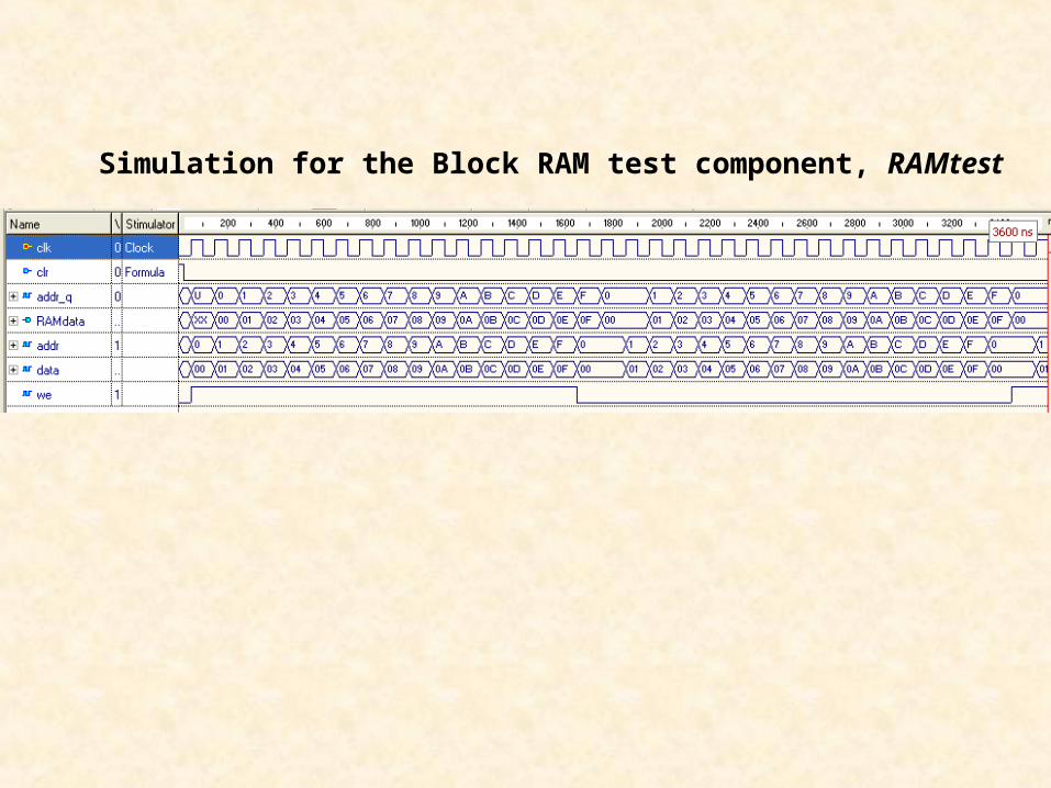
Simulation for the Block RAM test component, RAMtest

Design Summary--------------Logic Utilization: Number of Slice Flip Flops: 6 out of 3,840 1% Number of 4 input LUTs: 8 out of 3,840 1%Logic Distribution: Number of occupied Slices: 7 out of 1,920 1% Number of Slices containing only related logic: 7 out of 7
100% Number of Slices containing unrelated logic: 0 out of 7
0%Total Number of 4 input LUTs: 8 out of 3,840 1% Number of bonded IOBs: 10 out of 173 5% Number of Block RAMs: 1 out of 12 8% Number of GCLKs: 1 out of 8 12%Total equivalent gate count for design: 65,635Additional JTAG gate count for IOBs: 480Peak Memory Usage: 129 MB
Design Summary for RAMtest including the 16x8 Block RAM