reader et8017 electronic instrumentation, doc techniques
TRANSCRIPT

Chapter 2Dynamic Offset Cancellation Techniquesfor Operational Amplifiers
At low frequencies, offset, 1/f noise and drift are the dominant error sources ofoperational amplifiers. This is especially true in CMOS technology. This chapterreviews precision techniques that can be used to achieve low 1/f noise and lowoffset in operational amplifiers.
There are three types of CMOS offset cancellation techniques: trimming,chopping, and auto-zeroing. Trimming is usually performed during production toeliminate offset. Auto-zeroing is a sampling technique in which the offset ismeasured and then subtracted in subsequent clock phases. Chopping, on the otherhand, is a continuous-time modulation technique in which the signal and offset aremodulated to different frequencies. Due to the modulated offset and 1/f noise, achopper ripple appears at the amplifier output. Since chopping and auto-zeroingare dynamic techniques that continuously reduce offset, they also remove lowfrequency 1/f noise as well as offset drift over temperature or time.
In auto-zeroing amplifiers, the residual offset is mainly caused by chargeinjection and clock feed-through. While in chopper amplifiers, the residual offset ismainly caused by demodulated clock feed-through spikes. Several techniques canbe used to counteract these non-idealities.
Later in this chapter, several dynamic-offset-compensation techniques used inoperational amplifiers will be discussed, e.g. ping-pong auto-zeroing, offsetstabilization, and specifically, chopper offset stabilization of a low-frequency pathin a multi-path amplifier. To suppress chopper ripple, numerous ripple reductiontechniques can be used. It will be shown that these all have significant drawbacks,and thus new techniques are required.
R. Wu et al., Precision Instrumentation Amplifiers and Read-Out Integrated Circuits,Analog Circuits and Signal Processing, DOI: 10.1007/978-1-4614-3731-4_2,� Springer Science+Business Media New York 2013
21
2.1 Introduction
For sensor applications, the bandwidth of interest is generally a few Hz. In thisbandwidth, offset, 1/f noise and drift are the dominant error sources. Thus,dynamic offset cancellation techniques are required to mitigate these errors. Beforethose dynamic offset cancellation techniques are discussed, it is necessary to firstunderstand the nature and origins of these error sources.
2.2 Low Frequency Errors
2.2.1 Offset
In CMOS technology, the worst-case offset of a differential input pair can be aslarge as 10 mV [1]. This offset is caused by manufacturing variation or uncer-tainty. For example, MOS devices exhibit threshold voltage (Vth) mismatchbecause Vth is a function of the doping levels in MOS channels and the gates, andthese parameters vary randomly from one device to another.
On the other hand, the dimensions of MOS devices suffer from random,microscopic, variations during fabrication and hence there is mismatch betweenthe equivalent lengths and widths of nominally identical transistors. This mismatchcan be reduced by using large devices. However, this increases chip area andtherefore production cost.
2.2.2 1/f Noise
1/f noise is mainly caused by the defects in the interface between the gate oxideand the silicon substrate, so it depends on the ‘‘cleanness’’ of the oxide-siliconinterface and may be considerably different from one CMOS technology to another[2, 3]. The typical 1/f noise corner frequency of CMOStechnology is in the order ofseveral kHz to tens of kHz, making the 1/f noise a dominant error source at lowfrequencies. Related to the lifetime of the carriers, the 1/f noise can be modeled asa function of frequency [2], given by:
V2n ¼
K
WLCoxfð2:1Þ
where K is a process-dependent constant in the order of 10-25V2F, W and L are thewidth and length of the MOS transistor, Cox is the gate capacitance per unit area,and f is the operation frequency. Generally, 1/f noise in PMOS is much lower thanNMOS in most technologies.
22 2 Dynamic Offset Cancellation Techniques for Operational Amplifiers
In (2.1), the noise spectral density of the 1/f noise is inversely proportional tothe frequency. The inverse dependence of (2.1) on the area of the transistor WLsuggests that to decrease 1/f noise, the device area must be increased. However,this again increases chip area.
2.2.3 Drift
Drift is caused by the cross-sensitivity of some error sources to temperature ortime. Low drift is a critical requirement for precision temperature measurement(e.g. thermistor bridges and thermocouples), since the drift of the interface elec-tronics can then not be distinguished from the sensor signal itself.
Drift mainly manifests itself as offset drift and gain drift. Thus it can be reducedby suppressing the offset and gain error to a low enough level, and furthermore bydynamically compensating for their temperature drift.
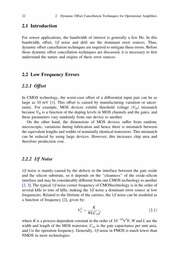
To conclude, Fig. 2.1 depict the low frequency errors in CMOS amplifier. Ascan be seen in the bandwidth of a few Hz for bridge transducer applications, themain errors are caused by 1/f noise, offset, and drift. To mitigate these errors,dynamic offset cancellation techniques can be employed, which will be describedin the next section.
2.3 Dynamic Offset Cancellation Techniques
To reduce offset, three types of offset cancellation techniques can be applied:trimming, auto-zeroing, and chopping. Trimming involves measuring and thenreducing the offset during production. While this approach can be used to obtain anorder-of-magnitude reduction of the offset, it is unable to reduce the initial mV-leveloffset below a few tens of lV, because offset drift is not compensated for. Moreover,trimming does not eliminate low-frequency noise, such as 1/f noise. Dynamic offsetcancellation techniques, such as auto-zeroing or chopping are therefore needed tocounteract this problem.
log(freq)
dB
Noise PSD
offset, drift
1/f noise
thermal noise
1/f corner frequency
10kHz10Hz
Fig. 2.1 Low frequencynoise spectrum for CMOSamplifier
2.2 Low Frequency Errors 23

2.3.1 Auto-Zeroing
Auto-zeroing is a discrete-time sampling technique. It involves sampling the offsetof the amplifier in one clock phase, and then subtracting it from the input signal inthe other clock phase. There are three basic topologies for auto-zeroing [4]: outputoffset storage (also called open-loop offset cancellation), input offset storage (alsocalled closed-loop offset cancellation) and closed-loop offset cancellation using anauxiliary amplifier.
2.3.1.1 Output Offset Storage
Figure 2.2 depicts an auto-zeroed amplifier with output offset storage. When CK ishigh, the amplifier is in the auto-zeroing phase in which its inputs are shortedtogether, driving its output to Vout = A�Vos. During this period, nodes X and Y areshorted together as well. When all the node voltages are settled, A�Vos is storedacross C1 and C2. When CK turns low, the amplifier enters the amplification phase.The differential input voltage together with Vos is amplified, and stored on C1 andC2. Since Vos is already stored on C1 and C2, VX and VY does not see Vos, which isfully cancelled.
When a switch opens, it injects some charge into the surrounding circuitry. Thischarge consists of gate-source/drain channel charge and charge injected throughthe overlap capacitances (also known as clock feed-through). In reality, the chargeinjection in the switches S3 and S4 will not completely cancel. The mismatchcharge injection results in a residual offset, given by
Vos;res ¼ ðqinj3
C1� qinj4
C2Þ=A; ð2:2Þ
where qinj3 and qinj4 are the charge injection caused by switches S3 and S4, A is theDC gain of the amplifier. Note that if A is large, A�VOS may saturate the amplifier’soutput. For this reason, A is typically chosen to be between 10 and 100 [2]. Anintegrated amplifier with three cascaded auto-zeroed amplifiers with output voltagestorage has been described in [4]. In [5], these stages were chopped, resulting in alow drift MOSFET operational amplifier.
Vos
Vin
CK
VCM
- +
VCM
A
C1
C2
CK
X
Y
S1 S2 S3 S4
Vout
Fig. 2.2 Auto-zeroing withoutput offset storage
24 2 Dynamic Offset Cancellation Techniques for Operational Amplifiers

2.3.1.2 Input Offset Storage
The output offset storage technique limits the maximum gain of the amplifier. If ahigh gain is needed, storing the offset at the input storage capacitance would be abetter solution. Figure 2.3 shows the basic principle of input offset storage tech-nique [2]. In the auto-zeroing phase when CK is high, the output and input of theamplifier are shorted together by switches S1 and S2, placing the amplifier in aunity-gain configuration.
When the node voltages are settled, the output voltage Vout is given by
Vout ¼A
1þ A� VOS: ð2:3Þ
The circuit reproduces the amplifier’s offset at nodes X and Y, storing the resulton C1 and C2. Note that for a zero differential input, the differential output is equalto VOS. Thus, the input-referred offset voltage of the overall circuit equals VOS/A ifS3 and S4 match perfectly.
If S3 and S4 have any mismatch, this will cause mismatch charge injection and,in turn, lead to a residual offset, which is given by
Vres �VOS
Aþ 1þ ðqinj3
C1� qinj4
C2Þ; ð2:4Þ
where qinj3 and qinj4 are the charge injection caused by switches S3 and S4, and A isthe DC gain of the amplifier.
From (2.4), the offset Vos is suppressed by the gain of the amplifier. The chargeinjection and the leakage of the capacitors can be reduced by increasing the size ofthe capacitors, but cannot be suppressed by the gain because the capacitors aredirectly at the amplifier input.
The drawback of input offset storage and output offset storage is that theyintroduce capacitors in the signal path. The bottom-plate parasitic of the capacitorsdecreases the amplifier bandwidth, thus degrading its phase margin and stability.
Vos
Vin
CK
VCM
A
CKS1 S2
+ -
C1
C2
Vout
S3
S4CK
X
Y
Fig. 2.3 Auto-zeroing withinput offset storage
2.3 Dynamic Offset Cancellation Techniques 25

2.3.1.3 Closed-Loop Offset Cancellation with Auxiliary Amplifier
To mitigate the stability issue, closed-loop offset cancellation with an auxiliaryamplifier can be used to isolate the offset storage capacitors from the signal path,as shown in Fig. 2.4.
In the auto-zeroing phase, the inputs of Gm1 are shorted. Thus, the outputvoltage Vout can be calculated as
½Gm1VOS1 � Gm2ðVout � VOS2Þ�R ¼ Vout;AZ ð2:5Þ
Thus,
Vout;AZ ¼Gm1RVOS1 þ Gm2RVOS2
1þ Gm2R: ð2:6Þ
This voltage is stored on C1 and C2 after S3 and S4 turn off. The offset voltagereferred to the main input is given by
VOS;res ¼Vout;AZ
Gm1R� VOS1
Gm2Rþ VOS2
Gm1R: ð2:7Þ
The charge injection due to the mismatch of S3 and S4 contributes to the offsetof Gm2. In order to attenuate this charge injection, as seen from (2.7), Gm2 isusually chosen to be at least 50 times smaller than Gm1.
Note that in an auto-zeroed amplifier, half of the clock period is used for auto-zeroing, so the amplified output is only available during part of the clock period.Such amplifiers cannot provide a continuous-time output, unless a ping-pongtopology is employed [4, 6].
As seen from the discussion above, these three offset cancellation techniquescancel offset by periodically subtracting the offset obtained during the previoussampling moment. This assumes that the offset does not change too much duringthe amplification time. Since low-frequency noise and DC offset can not be
Vos1
Vin
CK
VCM
Gm1
CKS1 S2
- +Vout
Gm2
C1C2
R
CK
Vos2
- +
S3
S4
Fig. 2.4 Auxiliary amplifier placed in a feedback loop during offset cancellation
26 2 Dynamic Offset Cancellation Techniques for Operational Amplifiers

distinguished from each other, these techniques also eliminate 1/f noise and drift.However, the sampling action of the auto-zeroing techniques affects the amplifier’snoise performance at frequencies below the sampling frequency [4].
2.3.1.4 Noise in Auto-Zeroing
As discussed above, auto-zeroing is a sampling technique. To complete settlewithin a half clock cycle, the noise bandwidth fn, BW (determined by the timeconstant of the system) is usually chosen to be larger than the auto-zeroing fre-quency fAZ, so that the under-sampled noise folds back to DC, increasing the noisePSD at the baseband.
The amount of folded noise to DC depends on the noise bandwidth fn, BW andthe auto-zeroing frequency fAZ. An exact quantitative calculation for the foldednoise of auto-zeroing can be found in [4, 7]. Since, this is rather complex, a moreintuitive explanation of noise folding in auto-zeroing is described here.
The noise folding factor n is defined as the ratio between the noise bandwidthand the auto-zeroing frequency, as given by
n ¼ 2fn;BW
fAZ
: ð2:8Þ
Due to under-sampling, the noise power after sampling increases by this factoras compared to that before sampling (Fig. 2.5), thus incurring a noise penalty. Thisimplies that by choosing a small fn, BW, the folded noise can be restricted.Applying this concept, a slow-settling nulling loop is used in [8, 9] to reduce thenoise bandwidth to a fraction of the auto-zeroing frequency. This approach will bediscussed in Sect. 2.3.2.
Noise Power
0 1 2 3-1-2-3 f/fs
Under-sampled noise
Input noise
Pno = (2fn,BW/fs)Pni
fs
2fn,BW
Fig. 2.5 Noise spectrum of asampled system
2.3 Dynamic Offset Cancellation Techniques 27

2.3.2 Chopping
Unlike auto-zeroing, chopping is a continuous-time modulation technique thatdoes not cause noise folding. Figure 2.6 shows a chopped amplifier together withits ideal waveforms. The input voltage Vin first passes through a chopper driven bya clock at frequency fch, thus it is converted to a square wave voltage at fch. Next,the modulated signal is amplified together with its own input offset. The secondchopper then demodulates the amplified input signal back to DC, and at the sametime modulates the offset to the odd harmonics of fch, where they are filtered out bya low-pass filter (LPF). This results in an amplified input signal without offset.
Low-frequency errors, such as 1/f noise and drift will be modulated and filteredout along with offset. This can be seen in Fig. 2.7, which depicts chopping in thefrequency domain. To completely remove the 1/f noise, the chopping frequencyshould be higher than the 1/f noise corner frequency. At the beginning, the signal ismodulated, and the noise and offset are superposed onto this modulated signal(Fig. 2.7b). After amplification and the second chopper, the modulated signal isdemodulated back to DC, while the low-frequency noise and offset are modulatedto the harmonics of the chopper frequency, appearing as a chopper ripple at theamplifier output (Fig. 2.7c). A LPF is then used to remove the modulated offsetand 1/f noise, resulting in a clean low-frequency signal without offset or 1/f noise(Fig. 2.7d).
From the above discussion, the offset is amplified by the DC gain of A1, whilethe signal is amplified by the effective gain of A1 at the chopping frequency fch, Tomaximize the effective gain of the stage consisting of A1 and two choppers, theoptimum chopping frequency should be around 3 dB bandwidth of A1 [4].
The amplitude of the chopper ripple can be calculated with the help of thesimplified block diagram shown in Fig. 2.8. The chopped offset of the input stageis filtered by the main Miller compensation capacitor CM1 and appears as a
Vos
DC AC
DC
Vin
Vos0
Vin
Vin
Vos
0
V1 /A1
0
V2 /A1
0
Vout /A
A1
fch fch
LPF +VoutVin
+V1 V2
+ +
+
fch fchfch
AC DC
DC AC ~0
Fig. 2.6 Chopping principlein the time domain
28 2 Dynamic Offset Cancellation Techniques for Operational Amplifiers

triangular waveform at the output. The peak-to-peak amplitude of the ripple canthen be approximated as:
Vout;ripple ¼Vos � Gm2
2CM1 � fch
: ð2:9Þ
From (2.9), ripple amplitude can be reduced by reducing input-stage offset Vos withcareful layout, by increasing the chopping frequency fch1 or by increasing the size of theMiller compensation capacitor. For a worst-case 20 mV offset, with Gm2 = 250 lA/V, CM1 = 80 pF, VDD = 5 V, and fch1 = 40 kHz, Vout, ripple & 0.8 V. This is quitelarge compared to the amplifier’s maximum 5 V output range and so must besuppressed.
2.3.3 Conclusions
Both auto-zeroing and chopping techniques have been introduced. Table 2.1compares and summarizes these two techniques. Chopping is superior to auto-zeroing because it is a continuous-time modulation technique that does not causenoise folding. However, chopping gives rise to a chopper ripple at the amplifieroutput. Auto-zeroing does not introduce ripple and its discrete-time nature is wellcompatible with switched-capacitor circuitry. Since power efficiency is an
Vin V1 V2
1 3 5 1 3 5 f/fchf/fch
signal
modulated signaloffset & noise
1 3 5 f/fch
Modulated offset & noise
1 3 5 f/fch
Vout
(a) (b) (c) (d)
Fig. 2.7 Chopping principle in the frequency domain
-
+
Vout
Gm2
Vos
+ -R2
R1
+
-Vin
+
-Va
-
+Gm1
CM11fch
CH1
CM12
fch
CH1
Fig. 2.8 Simplified block diagram of a chopper amplifier
2.3 Dynamic Offset Cancellation Techniques 29

important concern in our work, chopping is applied here. In Sect. 2.5.5, varioustechniques will be discussed to eliminate the chopper ripple.
2.4 Charge Injection Compensation Techniquesin Auto-Zeroed and Chopper Amplifiers
2.4.1 Compensation Techniques for Charge Injection
The residual offset of auto-zeroed amplifiers is mostly determined by chargeinjection and clock feed-through. To mitigate these two effects in a samplingcircuit, several techniques can be applied.
Dummy SwitchesCharge injection can be partially compensated for by adding dummy switches
that are driven by a complementary clock signal and that inject an amount ofcharge which compensates for the charge injected by the main switch [10]. Theeffectiveness of the compensation depends on the matching of the injected charges.A clock signal with a high slew rate can be used to obtain an equal distribution ofthe channel charge in the main switch’s drain and source terminals. A half-sizedummy switch can then be used for compensation (Fig. 2.9). However, theassumption of equal splitting of the charge between the source and drain is gen-erally invalid, making this approach less attractive.
Table 2.1 Comparison of auto-zeroing and chopping techniques
Auto-zeroing Chopping
Low frequency noise ± +Power-noise efficiency - +Ripple + -
Residual offset + ++
Note auto-zeroing removes 1/f noise, but causes the noise to fold back to DC, thus auto-zeroing interms of low-frequency noise is denoted as ‘‘±’’
Vout
CH
Vin
W/L
W/2L
qinj1 qinj2
Fig. 2.9 Charge injectioncompensation using dummyswitches
30 2 Dynamic Offset Cancellation Techniques for Operational Amplifiers

Using Complementary SwitchesAnother approach to reduce the charge injection is to use both PMOS and
NMOS devices such that the opposite charge packets injected by the two canceleach other (Fig. 2.10a). However, this cancellation is only effective for a limitedrange of the input signal around half of the supply voltage.
Using a Fully Differential CircuitThe best way to compensate for charge injection is to use fully differential
circuitry (Fig. 2.10b). If the charge injection in the two half circuits matches, thecharge injection only results in a change in the common-mode voltage. A differ-ential voltage change only results from charge-injection mismatch. With thiscompensation, a reduction in offset of at least 10 9 can be expected.
2.4.2 Charge Injection and Clock Feed-Through in ChopperAmplifiers
For chopper amplifiers, residual offset is mainly caused by the following threeissues:
• Non-idealities in clock timing• Demodulated clock feed-through current spikes• Impedance mismatch between two input nodes
Firstly, the non-idealities in the clock timing, such as clock skew, non-overlapand overlap in chopper clocks introduce residual offset. Clock skew is a phe-nomenon in which the two complementary chopper clocks switch at the differenttransition moments, as shown in Fig. 2.11a. Assuming the offset is 10 mV and theclock skew is 0.01 %, the resulting offset is 1 lV. To ensure a perfect offset
Vout
qinj1
Vin
CH
CK
CK
qinj2
Electrons
Holes
Vout1
CH
Vin1qinj1
Vout2
qinj2Vin2
CH
ΔV=Δqinj/CH
(a) (b)
Fig. 2.10 a Using complementary switches to reduce charge injection b Using differential circuitto suppress charge injection
2.4 Charge Injection Compensation Techniques in Auto-Zeroed and Chopper Amplifiers 31

cancellation, the two complementary chopping clocks must both exhibit 50 % dutycycle and have transitions at the same moments.
Having transitions at the same moment, means that both non-overlap andoverlap of the complementary chopper clocks must be avoided. An NMOSchopper is driven by the non-overlap chopper clocks, as depicted in Fig. 2.11b. Asmall time gap exists when clk1 and clk2 are both low, hence the differential signalpaths are being interrupted. This leaves the signal path not attenuated and maycause glitches at the output of the amplifier in between the choppers.
For the overlap chopper clocks (Fig. 2.11c), there is a small time interval whenboth clocks are high, thus causing a ‘‘short circuit’’ between the differential signalpaths. This causes low input impedance and also shorten the amplification timebetween the choppers. Thus, the effective gain of the amplifier reduces, resulting inincreased noise and offset.
Complementary chopper clocks with a 50 % duty cycle and the same transitions canbe produced by a non 50 % duty cycle clock and a divider-by-two D-flipflop, as will bedescribed in Sect. 4.6.5. Extra buffers can be added to reduce the rise and fall time.
Secondly, due to clock feed-through, the imbalance of parasitic capacitors in thechoppers also causes a residual offset [11]. Figure 2.12 illustrates the chargeinjection due to imbalanced parasitic capacitances of the input and output choppersin a fully-differential chopper amplifier. Figure 2.13 depicts a zoom-in picture ofthe input and output choppers in which the current spikes caused by imbalancedparasitic capacitances are illustrated.
50% 50%
49.99% 50.01%
clk1
clk2
clk1
clk2
clk1 clk2
clk1
clk2
(a) (b) (c)
Fig. 2.11 Non-idealities in clock timing a Clock skew b Non-overlap clock c Overlap clock
-
+ -
+
Vin
+
-
CH1 CH2
LPFVout+
-
+
-VLPFG1
C1
C2fCH
C3
C4
R1
R2
V1
+
-
V2
+
-
Ioffset
Fig. 2.12 Charge injection model in a chopper amplifier
32 2 Dynamic Offset Cancellation Techniques for Operational Amplifiers

As shown in the input chopper CH1 (Fig. 2.13a), at the transition moments ofthe chopper clocks, due to clock feed-through the mismatch between the capaci-tances C11 and C12 causes an AC current spike at the node of V1+. For the samereason, the mismatch between C21 and C22 also leads to another AC current spikeat V1-. The difference between these two current spikes results in an AC currentspike, as shown in Fig. 2.13a at V1. This AC current spike is rectified by CH1,which appears as a DC spike current at the input of CH1, with an average valuegiven by:
Ioffset;DC ¼ 2ðDC1�DC2Þ � VclkfCH ð2:10Þ
where DC1 = C11-C12, and DC2 = C21-C22, Vclk is the amplitude of the clocksignal, and fCH is the chopper frequency. The DC current spike contributes to theinput offset current Ioffset of the amplifier. This current goes through the seriesimpedance of the chopper and the input signal source, leading to a rectified inputvoltage spike. The average DC value of the spike results in a residual offsetVOS, res1, as given by:
VOS;res1 ¼ 2ðR1 þ R2Þ � ðDC1�DC2Þ � VclkfCH ð2:11Þ
where (R1 ? R2) is the input impedance including on-resistance of the chopperswitches and the impedance of the signal source. DC1 and DC2 are the mismatch ofclock feed-through capacitances, which is mainly due to the overlap capacitancesof the clock line and the source terminals of switches in the input chopper CH1. IfDC1 = DC2, then no residual offset occurs since it will only result in a common-mode spike.
DC3 and DC4 are the mismatch of clock feed-through capacitances due to theoverlap capacitances of the clock lines and the amplifier G1 output. They will alsocause an AC current spike at V2 (Fig. 2.13b). To provide this AC current spike, theinput of G1 needs to generate an AC voltage spike. This voltage spike is
C11
C12C21
C22
fCH fCH
C32
fCH fCH
C31
C41
C42
M11 M22
M12
M21
M31
M32
M42
M41
Vin
+
-
V1
+
-
V2
+
-
Vout
+
-
00
IDC,offset
0
Input chopper CH1 Output chopper CH2
IAC,spike IAC,spike
(a) (b)
Fig. 2.13 Current spikes caused by imbalanced parasitic capacitances in the input and outputchoppers CH1 and CH2 that give rise to a residue offset
2.4 Charge Injection Compensation Techniques in Auto-Zeroed and Chopper Amplifiers 33

demodulated by the input chopper towards the input, resulting in a residual offsetVOS, res2 as given by:
VOS;res2 ¼2ðDC3�DC4ÞVclkfCH
G1ð2:12Þ
where DC3 = C31-C32, DC4 = C41-C42, and G1 is the transconductance of thechopped amplifier. It can be seen that an amplifier with a higher transconductanceis less vulnerable to the mismatch of DC3 and DC4. For example, a 10 kHzchopper frequency with 1/G1 = 5 kX, no source impedance, and a 5 V drivingclock voltage would result in a residual offset per unit of capacitance mismatchbetween DC3 and DC4 of 0.5 l V/fF. The total residual offset due to clock feed-through is the sum of the offsets given in (2.11) and (2.12).
Thirdly, the source impedance mismatch (DR = R1-R2) causes another residualoffset. The charge injection and clock feed-through due to chopping action cause twos (denoted as Ibias in Fig. 2.14) which both flow out of the amplifier’s input in thesame direction [12]. For bias current calculation, if DC1 = DC2 = DC as shown inFig. 2.14, the average value of the bias current Ibias (Fig. 2.14) can be calculated as:
Ibias;DC ¼ 2DC � Vclk � fCH ð2:13Þ
The mismatch between input impedances R1 and R2 is DR, so these two biascurrents also generate residual offset, given by:
VOS;res3 ¼ 2ðR1�R2Þ � DC � Vclk � fCH ð2:14Þ
If DC is 1fF, the chopper frequency fCH is 10 kHz with a 5 V chopper clock,then according to (2.13), the resulting bias current is 0.1 nA. From (2.14), if themismatch between R1 and R2 is 100 kX, these two bias currents flow through thesetwo resistors (Fig. 2.14), resulting in an extra residual offset of 10 lV.
It can be seen from (2.11), (2.12) and (2.14) that, the charge injection and clockfeed-through of the choppers, cause input bias current, offset current and hence theresidual offset. These three errors can be minimized by:
• Decreasing the chopping frequency• Decreasing the chopper clock amplitude• Balancing or minimizing the overlap capacitors between the clock lines to the
input and output terminals of G1
-
+ -
+
Vin
+
-
CH1 CH2
LPFVout+
-
+
-VLPFG1
CCfCH
R1
R2
V1
+
-
V2
+
-
Ibias
Ibias
C
C
Fig. 2.14 Residual offset due to the bias current and impedance mismatch in a chopper amplifier
34 2 Dynamic Offset Cancellation Techniques for Operational Amplifiers

• Ensuring matched and balanced input impedance for differential paths reducesresidual offset caused by the input bias current
In Chap. 4, a chopper layout that minimizes the charge injection and clock feed-through will be presented.
2.4.3 Chopper Charge Injection Suppression Techniques
Besides minimizing the charge injection and clock feed-through with the afore-mentioned methods, there are several techniques that can be used to suppress thedemodulated clock feed-through spikes.
Nested-Chopper TechniqueSince the residual offset of a chopper amplifier is proportional to the chopper
frequency fch, as expressed by Eqs. (2.11), (2.12) and (2.14), it can be decreased byreducing fch. However, fch cannot be lower than the 1/f noise corner, otherwise1/f noise can not be completely removed. The nested chopper technique solves thisproblem by using an extra pair of choppers that run at a much lower frequency.The residual offset of the amplifier chopped by a high frequency chopper clock UH
is chopped out by a low-frequency chopper clock UL [13] (Fig. 2.15).
-
+ -
+
Vin
+
-
Vout
+
-
ALPF
L LH H
V1
-
+V2
-
+V3
-
+
V1 /A
t
t
0
t
Vspike
-Vspike
Vspike
-Vspike
Vspike
-Vspike
0
0
V2 /A
V3 /A fH=3•fL
Vos,res,H
(a)
(b)
Fig. 2.15 a Nested chopper amplifier b Charge-injection spikes from the high-frequencychoppers are chopped by the low-frequency chopper pair
2.4 Charge Injection Compensation Techniques in Auto-Zeroed and Chopper Amplifiers 35

The overall residual offset is only limited by the charge injection in the low-frequency chopper, and therefore it is reduced by a factor fH/fL, where fH and fL arehigh and low chopping frequencies, respectively.
The implementation of the nested chopper is very simple: only one extra pair ofchoppers and a low-frequency clock signal are needed. A disadvantage of thisapproach is that the useable signal bandwidth is reduced, since it is limited by fLrather than fH. However, this is not a problem for bridge read-out applications.Nested chopping can be used to chop the complete read-out chain which consistsof a preamp and a DR ADC. The low-frequency chopper spikes at fL can be filteredout in the decimation filter following the DR ADC [14]. The nested chopping willbe applied to the read-out IC design, as will be discussed in Chap. 5.
Filtering of Spike HarmonicsThe chopper clock is a square-wave signal that contains odd harmonics at fch,
3fch, 5fch, etc. Most of the energy of the chopper ripple is located at the firstharmonics [4]. Therefore, a low-pass (LP) or band-pass (BP) filter can be incor-porated between the chopper switches to filter out the chopper harmonics at thehigh frequencies, at the cost of a small reduction in the signal bandwidth [4](Fig. 2.16a). A LP filter was implemented in [15] to filter the spikes, achieving a5 lV offset (Fig. 2.16b). A BP filter implementation is presented in [16] to sup-press the DC offset. Here, the chopping frequency is designed to track the centerfrequency of the BP filter. It achieves an offset of less than 600 nV. However, adisadvantage of this technique is the significant amount of extra circuitry required.
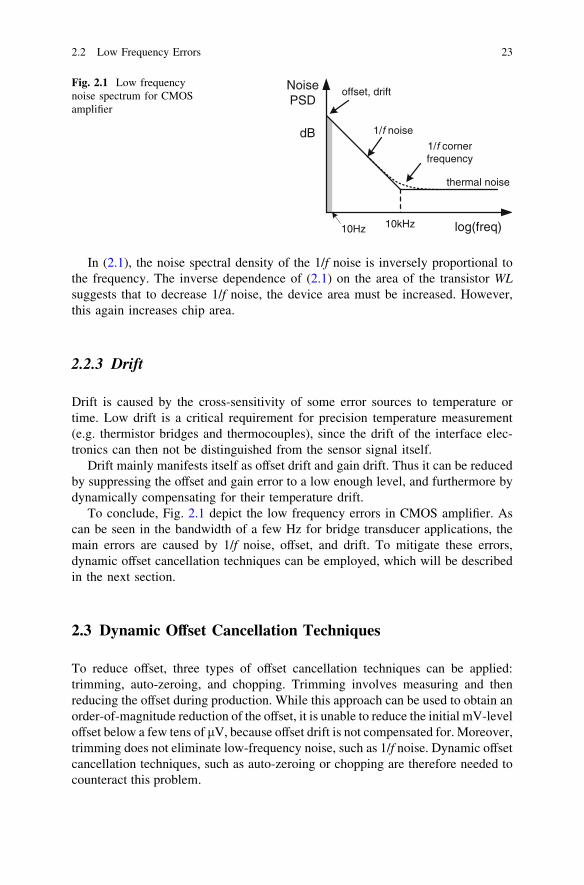
Chopper with Guard BandAnother approach to filter out clock feed-through spikes is to introduce a small
guard time in the output chopper switch that prevents the spikes caused by theinput chopper from being demodulated, as shown in Fig. 2.17b. This technique has
-
+ -
+
Vin
+
-
Vout
+
-
A1LPF
fch
-
+ -
+A2
or
R1
R2
fch0 3fch 5fch 7fch
V1
+
-
V1(a)
(b)
Fig. 2.16 a Modulated signal and spike harmonics of V1 b Chopper amplifier with an LP or BPamplifier to remove clock feed-through spikes
36 2 Dynamic Offset Cancellation Techniques for Operational Amplifiers
been used in [17–19] for custom sensor interfaces. An average offset of 200 nVhas been achieved in [18]. However, the residual offset with the guard bandtechnique is limited by the matching between the shape of the spike and the guardtime delay. Moreover, the output signal is no longer continuous-time due to thegap in the guard time since Vout just holds the value before the guard time starts,thus incurring a slight loss of gain and noise aliasing.
2.4.4 Conclusions
For the auto-zeroed amplifier, charge injection determines the residual offset. Inthe chopper amplifier, the residual offset is caused by the non-ideality in clocktiming, the demodulated clock feed-through current spikes and the impedancemismatch between two input nodes. To conclude, symmetry, matching and bal-ancing the parasitics are essential to achieve low residual offset in chopperamplifier.
2.5 Dynamic Offset Compensated Operational Amplifiers
This section discusses the basic principle of feedback and then reviews severalprecision operational amplifiers that employ the dynamic offset cancellationtechniques discussed above, i.e. auto-zeroing and chopping. These amplifiertopologies include ping-pong, offset stabilization and chopper offsetstabilization.
-
+ -
+
Vin
+
-Vout
+
-
A1
fM
M D
fD
Va
+
-Vb+
-
Va
fM
fD
tVout
Average is 0
(a)
(b)
Fig. 2.17 a Modulatedamplifier b Guard band clockdiagram
2.4 Charge Injection Compensation Techniques in Auto-Zeroed and Chopper Amplifiers 37

2.5.1 Feedback
Feedback is a powerful technique that has found wide application in high-precisionsignal processing. Figure 2.18 shows a negative feedback system, where H(s) andb denote the high gain amplifier and the passive feedback network, respectively.Part of the output signal is redirected back to the input and compared to theincoming signal. The loop accurately controls the output to produce an amplifiedor processed replica of the input signal.
The error, which is indicated as E in Fig. 2.18, is given by:
EðsÞ ¼ XðsÞ � bYðsÞ ¼ XðsÞ 11þ bHðsÞ ð2:15Þ
From (2.15), the higher the loop gain bH(s), the more effectively the error E isminimized. This means that a feedback loop with high loop gain can be applied toreduce an error.
This feedback concept will be used in the work presented in Chaps. 4 and 5 toreduce the offset and gain error of an amplifier. Generally, the feedback concept isused in operational amplifiers to obtain an accurate gain determined by 1/b. Thenext few sections will review several precision operational amplifier topologies.
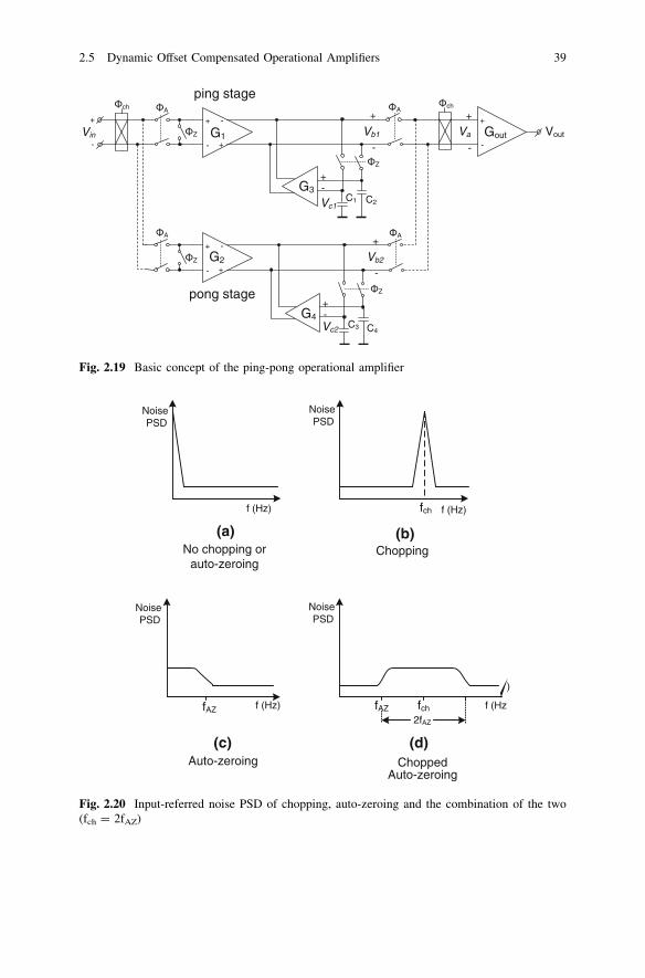
2.5.2 Ping-Pong Operational Amplifier
As discussed before, the auto-zeroing technique is not directly suitable for use in acontinuous-time general purpose amplifier, since the amplified output signal isonly available during one half of the clock period. To obtain a continuous-timeoutput signal, the ping-pong technique can be used. This involves the use of twoauto-zeroed amplifiers [6], as shown in Fig. 2.19. When one amplifier is beingauto-zeroed, the other is being used to amplify the signal. The same output stage isshared by the two auto-zeroed amplifiers. Furthermore, the combination of auto-zeroing and chopping is employed to achieve a noise PSD of 20 nV/HHz from DCto 1.5 kHz, which rises to 48 nV/HHz at 20 kHz. It consumes a supply current of800 lA.
Figure 2.20 shows the noise spectrum of chopping, auto-zeroing and thecombination of these two. As seen from Fig. 2.20b, chopping modulates low-frequency 1/f noise to the chopping frequency, thus achieving a clean and flat noise
H(s) Y(s)+
–
X(s)E
Fig. 2.18 Block diagram ofa general feedback system
38 2 Dynamic Offset Cancellation Techniques for Operational Amplifiers
-
+ -
+
+
-Vin G1
A
ping stage
-
+
Gout Vout
G3
-
+ -
+G2
A
pong stage
G4
Z
Z
ch
C1 C2
C3 C4
Vb1
Vb2
Vc2
Vc1
+
-
+
-
+-
+-
A
A
Z
Z
ch
Va
+
-
Fig. 2.19 Basic concept of the ping-pong operational amplifier
f (Hz)
Noise PSD
f (Hz)
Noise PSD
fch
f (Hz)
Noise PSD
fAZ f (Hz
)
fAZ
2fAZ
fch
(a) (b)
(c) (d)
No chopping or auto-zeroing
Chopping
Auto-zeroing Chopped Auto-zeroing
Noise PSD
Fig. 2.20 Input-referred noise PSD of chopping, auto-zeroing and the combination of the two(fch = 2fAZ)
2.5 Dynamic Offset Compensated Operational Amplifiers 39

spectrum at low frequencies, but with ripple at the chopping frequency. Auto-zeroing involves sampling, thus causing increased noise at DC due to aliasing(Fig. 2.20c). In their combination, since the input stage is chopped at twice theauto-zeroing frequency, this noise is then modulated away from DC to fch (or 2fAZ)[6] (Fig. 2.20d).
A disadvantage of the ping-pong technique is that spikes are introduced becausethe voltages Vb1 and Vb2 at the output of the first stage amplifiers have to switchbetween the offset compensating voltages Vc1, Vc2 and the voltage required at theinput of the output amplifier Va. This results in spikes at the output. This effect canbe reduced by replacing C1-C4 with active integrators with the same input CMvoltage as the output stage Gout [1]. However, spikes still remain becauseswitching occurs within the signal path.
2.5.3 Chopper-CDS Operational Amplifier
As a hybrid of chopping and auto-zeroing, a ripple-free operational amplifier isproposed in [20] that uses input chopping and correlated double sampling (CDS)for demodulation. As shown in Fig. 2.21, the AC-coupling capacitor Ccds isinserted between the first and the second stage, removing the offset from the firststage without causing ripple. The CDS then demodulates the signal back to DC.
Since CDS operates on the modulated input signal, the folded noise spectrumdue to sampling is also around the fCDS, which is equal to the chopping frequency.This implies that the gain of A1 around the chopping frequency fch should be largesince it suppresses the folded noise of CDS. The DC gain of A1 should be lowenough so that the amplified offset and 1/f noises do not saturate A1. A1 isimplemented with a band-pass response that exhibits low gain around DC but highgain at fch. In the worst case, the amplified offset can still be too large. A band-reject passive feedback network is used that decreases the gain at low and highfrequencies, but not at the chopping frequency. In this way, the DC gain of A1 isreduced further. However, this scheme increases the circuit complexity. It achievesa 2 lV offset and a noise PSD of 37nV/HHz with an NEF of 5.5.
Vos
A1
fch
+Vin
CDS A2Vout
CcdsVo
fch1
2 1
CS
1 2
Fig. 2.21 Simplifiedchopper-CDS block diagram
40 2 Dynamic Offset Cancellation Techniques for Operational Amplifiers
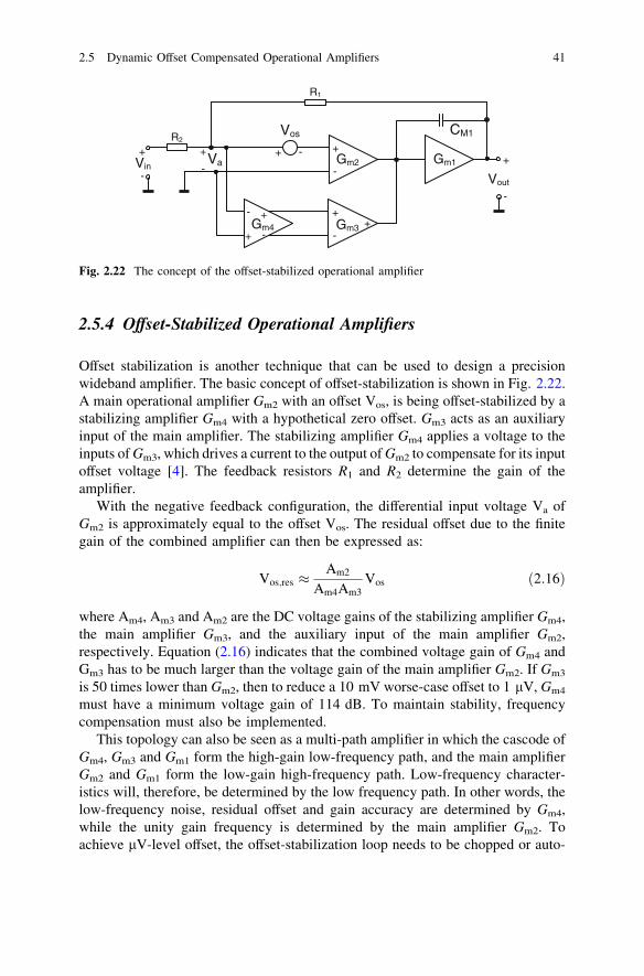
2.5.4 Offset-Stabilized Operational Amplifiers
Offset stabilization is another technique that can be used to design a precisionwideband amplifier. The basic concept of offset-stabilization is shown in Fig. 2.22.A main operational amplifier Gm2 with an offset Vos, is being offset-stabilized by astabilizing amplifier Gm4 with a hypothetical zero offset. Gm3 acts as an auxiliaryinput of the main amplifier. The stabilizing amplifier Gm4 applies a voltage to theinputs of Gm3, which drives a current to the output of Gm2 to compensate for its inputoffset voltage [4]. The feedback resistors R1 and R2 determine the gain of theamplifier.
With the negative feedback configuration, the differential input voltage Va ofGm2 is approximately equal to the offset Vos. The residual offset due to the finitegain of the combined amplifier can then be expressed as:
Vos;res �Am2
Am4Am3
Vos ð2:16Þ
where Am4, Am3 and Am2 are the DC voltage gains of the stabilizing amplifier Gm4,the main amplifier Gm3, and the auxiliary input of the main amplifier Gm2,respectively. Equation (2.16) indicates that the combined voltage gain of Gm4 andGm3 has to be much larger than the voltage gain of the main amplifier Gm2. If Gm3
is 50 times lower than Gm2, then to reduce a 10 mV worse-case offset to 1 lV, Gm4
must have a minimum voltage gain of 114 dB. To maintain stability, frequencycompensation must also be implemented.
This topology can also be seen as a multi-path amplifier in which the cascode ofGm4, Gm3 and Gm1 form the high-gain low-frequency path, and the main amplifierGm2 and Gm1 form the low-gain high-frequency path. Low-frequency character-istics will, therefore, be determined by the low frequency path. In other words, thelow-frequency noise, residual offset and gain accuracy are determined by Gm4,while the unity gain frequency is determined by the main amplifier Gm2. Toachieve lV-level offset, the offset-stabilization loop needs to be chopped or auto-
-
+
-
+-
+ -
+
Vout
Gm2
Gm3 +Gm4
Vos
+ -R2
R1
+
-Vin
+
-Va
-
+Gm1
CM1
Fig. 2.22 The concept of the offset-stabilized operational amplifier
2.5 Dynamic Offset Compensated Operational Amplifiers 41
zeroed. Chopping is more power-efficient than auto-zeroing, therefore chopperoffset-stabilized amplifiers will be discussed in the next section.
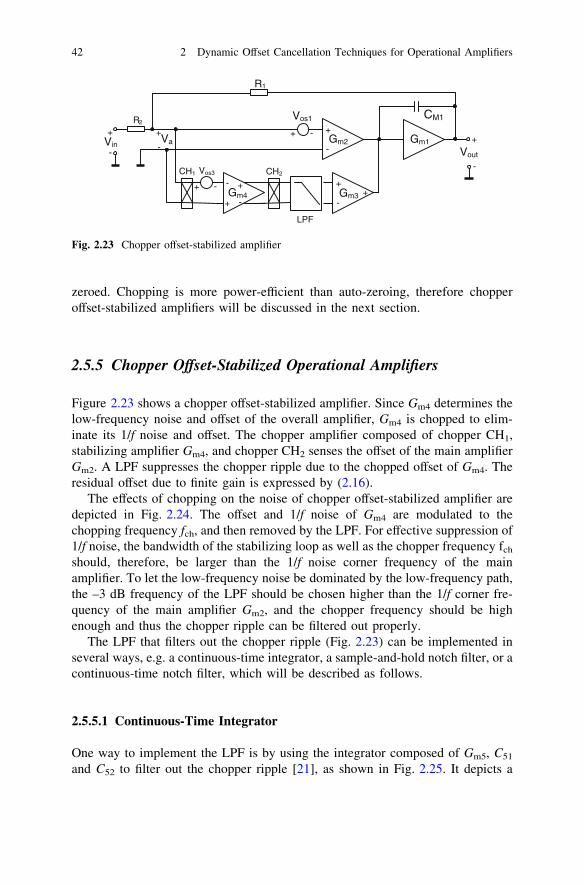
2.5.5 Chopper Offset-Stabilized Operational Amplifiers
Figure 2.23 shows a chopper offset-stabilized amplifier. Since Gm4 determines thelow-frequency noise and offset of the overall amplifier, Gm4 is chopped to elim-inate its 1/f noise and offset. The chopper amplifier composed of chopper CH1,stabilizing amplifier Gm4, and chopper CH2 senses the offset of the main amplifierGm2. A LPF suppresses the chopper ripple due to the chopped offset of Gm4. Theresidual offset due to finite gain is expressed by (2.16).
The effects of chopping on the noise of chopper offset-stabilized amplifier aredepicted in Fig. 2.24. The offset and 1/f noise of Gm4 are modulated to thechopping frequency fch, and then removed by the LPF. For effective suppression of1/f noise, the bandwidth of the stabilizing loop as well as the chopper frequency fch
should, therefore, be larger than the 1/f noise corner frequency of the mainamplifier. To let the low-frequency noise be dominated by the low-frequency path,the –3 dB frequency of the LPF should be chosen higher than the 1/f corner fre-quency of the main amplifier Gm2, and the chopper frequency should be highenough and thus the chopper ripple can be filtered out properly.
The LPF that filters out the chopper ripple (Fig. 2.23) can be implemented inseveral ways, e.g. a continuous-time integrator, a sample-and-hold notch filter, or acontinuous-time notch filter, which will be described as follows.
2.5.5.1 Continuous-Time Integrator
One way to implement the LPF is by using the integrator composed of Gm5, C51
and C52 to filter out the chopper ripple [21], as shown in Fig. 2.25. It depicts a
-
+
-
+-
+ -
+
Gm2
Gm3 +Gm4
Vos1
+ -+
-Vin
+
-Va
Vos3
+ -
CH1
LPF
R2
R1
CH2
Gm1
CM1
Vout
-
+
Fig. 2.23 Chopper offset-stabilized amplifier
42 2 Dynamic Offset Cancellation Techniques for Operational Amplifiers

multi-path architecture that employs this technique in combination with hybridMiller compensation [22, 23]. The gain stages Gm2 and Gm1 form the high-fre-quency low-gain path, while the transconductances Gm4, Gm5, Gm3 and Gm1 formthe high-gain low-frequency path. To realize a frequency response with a smoothroll-off, the unity gain frequency of both paths should be [23].
f0dB ¼Gm4
2pC3¼ Gm2
2pC1ð2:17Þ
where C3 and C1 are the values of capacitors C31 (or C32) and C11 (or C12),respectively.
The modulated offset Vos4 of Gm4 is filtered by the integrator consisting of Gm5,C51 and C52. However, the integrator needs very large capacitors to obtain a lowcut-off frequency. Hence in reality, a residual chopper ripple in the form of atriangular wave appears at the integrator output. Furthermore, due to the action ofthe chopper CH2, the offset of Gm5 (Vos5) appears as a square-wave voltage overthe capacitor Cp4, charging and discharging this capacitor. The resulting
f (Hz)
NoisePSD
f (Hz)
NoisePSD
fch
LPF
f (Hz)
NoisePSD
fch
Noise of chopper offset-stabilized amplifier
Noise of Gm3 Noise of chopped Gm3 and LPF
(a) (b) (c)
Fig. 2.24 Noise in chopper-stabilized amplifiers
CH1
-
+ -
+ -
+Gm1
-
+
-
+ -
+CH2
-
+ -
+
VoutVin
+
-Gm2
Gm4
Cp4
Gm3
C11
C12
C31
C32
Vos4
Vos2
-
+ -
+Gm5
C51
C52
Vos5
R2
+
-
R1
Fig. 2.25 Chopper offset-stabilization amplifier using an active integrator and multi-path hybrid-nested Miller compensation
2.5 Dynamic Offset Compensated Operational Amplifiers 43

alternating current at the output of Gm4 is demodulated by chopper CH1, causing aresidual offset.
To eliminate this residual offset, the parasitic capacitor Cp4, or the offset Vos5 ofthe integrator, must be minimized. The parasitic capacitor Cp4 can be minimizedby choosing small dimensions for the transistors that are connected to the outputterminals of Gm4. Furthermore, Cp4 can be minimized to ensure a fully symmetricand balanced layout. To reduce offset Vos5, auto-zeroing can be used [21].However, it increases the complexity and power consumption of the design. Sincethe focus of this thesis is to design a low- noise amplifier with good noise-powerefficiency, the topology with Gm5 auto-zeroed will not be elaborated further.
2.5.5.2 Sample-and-Hold Notch Filter
An alternative solution for implementing the LPF in Fig. 2.23 are to use a swit-ched-capacitor (SC) sample-and-hold circuit to sample the chopper ripple at theoutput of the integrator, as shown in Fig. 2.26. It shows an operational amplifierwith multi-path hybrid-nested Miller compensation. A LPF is implemented with aSC notch filter consisting of the switches driven by U1 and U2 and the capacitorsC53 and C54 [24]. The switches sample the chopper ripple at the zero-crossingpoints. The notch positions of the Sinc filter are located at multiples of the chopperfrequency, and thus are accurately determined by the chopping clock.
This notch filter acts as a passive integrator. To compensate for the extra poleintroduced by the notch filter, the capacitors C51 and C52 are introduced for thesame reason as the hybrid-nested Miller compensation [23]. Capacitors C31 andC32 are theoretically not needed, but they help to maintain local loop stability. Thecapacitor C3 helps to limit the bandwidth of the low-frequency path so that thedelay caused by the notch filter does not cause instability [24].
However, this technique still involves sampling, and so still incurs a certainnoise-folding. More importantly, the sample-and-hold filter exhibits a Sinc
CH1
-
+ -
+ -
+Gm1
-
+
-
+ -
+CH2
-
+ -
+
Gm2
Gm4
Cp4
C53
C54
Gm3
C11
C12
C51
C52
C3
C31
C32
Vos4
Vos2
1
1
2
2
R2
Vin
+
- Vout
+
-
R1
Fig. 2.26 Multi-path operational amplifier with an embedded sample-and-hold circuit
44 2 Dynamic Offset Cancellation Techniques for Operational Amplifiers

filtering response, creating a significant phase shift at the chopping frequency.Overcoming these phase shift complicates the frequency compensation in theamplifier.
2.5.5.3 Continuous-Time Notch Filter
As a counterpart of SC implementation, the notch filter also can be implemented ina continuous-time (CT) fashion. Figure 2.27 shows a CT notch filter incorporatedin the low-frequency path to filter out the chopper ripple [25] in a multi-pathoperational amplifier. Additionally, a buffer A1 is used to allow feedback through acompensation capacitor C1a for the low-frequency path, thus preventing thechopper ripple at the output of CH2 from feeding forward through C1a to the outputof the amplifier.
The disadvantage of this approach is that the notch filter suppresses the ripple inan open-loop structure. This implies that the chopping frequency derived from thetime constant of the on-chip relaxation oscillator needs to be well-matched to thenotch position of the CT filter, which is also determined by the product of certainresistors and capacitors. This frequency tracking is not an issue for the SC notchfilter [24], since the notch positions are precisely determined by the choppingclock. Furthermore, if a tunable chopping frequency is desired, a phase-lockedloop (PLL) is then required to track the external chopping frequency to ensure thatthe RC time constant of the CT notch filter closely tracks the locking frequency.Otherwise, trimming is required to tune the notch location in the CT notch filter.
2.5.5.4 Auto-Correction Feedback Loop
Another way to suppress the chopper ripple is to use an auto-correction feedback(ACFB) loop to null the offset in a chopper multi-path operational amplifier [26, 27].
-
+
-
+ -
+ -
+
C3
Gm4Gm5
Gm1 Gm3
CH1 CH2
-
+Gm2
Continuous-time notch filter
C1b
C1aA1
-
+
+
-
R2
Vin
+
- Vout
+
-
R1
Fig. 2.27 Multi-path operational amplifier with an embedded continuous-time notch filter
2.5 Dynamic Offset Compensated Operational Amplifiers 45

Its block diagram is shown in Fig. 2.28. Unlike the designs presented in [24, 25]which employ notch filters in the signal path to suppress the chopper ripple, thisapproach uses a feedback loop outside the signal path. Therefore, it does not causeany phase shift in the signal path. However, the stability of the feedback loop itselfneeds to be taken care of. This is because the notch filter creates a significant phaseshift at the chopping frequency, and the unity gain frequency of the ACFB loop mustoccur well below the chopping frequency to ensure the loop stability. Increasing theunity-gain frequency speeds up the settling of the loop. However, a higher choppingfrequency is then required, thus increasing the charge injection and the offset.
Moreover, since the sensing points of the loop are the virtual ground of Gm2,they are relatively ‘‘quiet’’. The DC gain of the loop is limited because of the smallripple excitation. A ripple reduction of only 43 dB [26] is achieved. Furthermore,the SC notch filter (NF) causes sampling noise at DC. This noise is modulated byCH2 and creates a peak output noise PSD around the chopping frequency.
2.6 Conclusions
Table 2.2 summarizes the performances of precision operational amplifiers thatachieve lV-level offset. They apply different techniques to suppress chopperripple. One technique is to use auto-zeroing to reduce the initial offset of theamplifier [6, 21]. However, the increased low-frequency noise due to noise foldingleads to a noise penalty, i.e. extra power dissipation is needed to meet a givennoise specification (NEF = 21.8 and 153). A band-pass filter can be implementedbetween the choppers to suppress the DC offset, so as to eliminate the output
-
+-
-
+ -
+ -
+
-
+-
+
C1
Gm5Gm6
Gm1
Gm4
Gm2
CH1 CH2
C32
C31
SC Notch Filter
-
+-
+Gm3
CH3
Vin
+
-
R2
R1
Vout
+
-
Fig. 2.28 Multi-path operational amplifier with an auto-correction feedback loop
46 2 Dynamic Offset Cancellation Techniques for Operational Amplifiers

chopper ripple [16]. However, the chopping frequency needs to track the centerfrequency of the band-pass filter, which requires significant amount of extracircuitry.
A switched-capacitor [24] or a continuous-time notch filter [25] can be embeddedin a multi-path offset stabilized operational amplifier to reduce the chopper ripple.However, the SC notch filter [24] involves sampling thus causing noise folding. Theissue associated with the CT notch filter [25] is that the notch filter suppressesthe ripple in an open-loop structure. To effectively suppress the chopper ripple, thenotch frequency of the CT filter needs to closely track the chopping frequency,which could be limited by the RC spread in the CT notch filter. Another techniqueuses an auto-correction feedback loop [26] to suppress the chopper ripple. However,since the ripple sensing points are at the ‘‘quiet’’ virtual grounds of the output stage,the limited loop gain restricts the ripple suppression ratio.
In addition, the notch filters generate excess phase shift, meaning that thechopper clock frequency must be relatively high ([ 125 kHz) to maintain stabilityin the signal path [24, 25] or in the feedback loop [26]. Such a high choppingfrequency increases charge injection errors, and hence increases input offset, giventhe same noise level and process parameters. The chopper-CDS scheme [20] usesan AC-coupled capacitor to block the offset, thus generating no chopper ripple.However, this technique also necessitates a high chopping frequency of 500 kHz,resulting in a relatively low input impedance and a high input bias current.
Therefore, innovative solutions need to be explored to eliminate the chopperripple without causing the above-mentioned issues: noise aliasing, frequencytracking, limited loop gain, and excess phase shift (high chopping frequencies).To counteract these problems, a new ripple reduction technique will be proposedin Chap. 4.
Table 2.2 Comparison of precision operational amplifiers
Tang [6] Witte [21] Burt [24] Kusuda [27] Belloni [20]
Year 2002 2006 2006 2011 2010Noise PSD (nV/HHz) 20 15 55 5.9 37Chopping frequency(kHz)
15 32 125 200 500
Offset (lV) 3 1.5 3 0.78 1.94Input bias current (pA) 40 – 70 72 –GBW (kHz) 2500 1370 350 4000 260Supply current (Iq)(lA) 800 700 17 1470 14.4Die area(mm2) 0.67 3.6 0.7 1.26 1.14NEF [28] 21.8 153 8.7 8.7 5.5GBW/Iq (kHz/lA) 3.1 2 20.6 2.7 18Rail sensing capability No Yes Yes Yes YesRipple reductiontechnique
Auto-zeroing
Auto-zeroedintegrator
SC notchfilter
Autofeedback loop
Chopper-CDS
2.6 Conclusions 47

References
1. Witte JF (2008) Dynamic offset compensated CMOS amplifiers. Ph.D. Thesis, DelftUniversity of Technology, The Netherlands
2. Razavi B (2001) Design of analog CMOS integrated circuits. McGraw-Hill Companies, Inc.,New York
3. Sansen WMC (2006) Analog design essentials. Springer, Dordrecht4. Enz CC, Temes GC (1996) Circuit techniques for reducing the effects of op-amp
imperfections: auto-zeroing, correlated double sampling, and chopper stabilization. Proc.IEEE 84(11):1584–1614
5. Poujois R, Borel J (1978) A low drift fully integrated MOSFET operational amplifier. IEEE JSolid-State Circuits 13:499–503
6. Tang ATK (2002) A 3 lV-offset operational amplifier with 20nV/HHz input noise PSD atDC employing both chopping and auto-zeroing. In Proceedings of the IEEE ISSCC, Dig.Tech. Papers, pp 386–387
7. Enz CC (1989) High precision CMOS micropower amplifiers. Ph.D. Thesis, Thesis no. 802,Ecole Polytechnique Federale de Lausanne (EPFL). Available at: http://library.epfl.ch/en/theses/?nr=802,1989
8. Pertijs MAP, Kindt WJ (2009) A 140 dB-CMRR current-feedback instrumentation amplifieremploying ping-pong auto-zeroing and chopping. In Proceedings of the IEEE ISSCC, Dig.Tech. Papers, pp 324–325
9. Pertijs MAP, Kindt WJ (2010) A 140 dB-CMRR current-feedback instrumentation amplifieremploying ping-pong auto-zeroing and chopping. IEEE J Solid-State Circuits 45(10):2044–2056
10. Wegmann G, Vittoz EA, Rahali F (1987) Charge injection in analog MOS switches. IEEE JSolid-State Circuits, SC-22(6):1091–1097
11. Witte JF, Makinwa KAA, Huijsing JH (2004) The effect of non-idealities in CMOS chopperamplifiers. In Proceedings of the ProRISC 2004, pp 616–619
12. Fan Q, Huijsing JH, Makinwa KAA (2011) Analysis of input impedance, input bias and offsetcurrent of a chopped multi-path current feedback instrumentation amplifier. In Proceedings ofthe IWASI, pp 61-66
13. Bakker A, Thiele K, Huijsing JH (2000) A CMOS nested-chopper instrumentation amplifierwith 100-nV offset. IEEE J Solid-State Circuits 35(12):1877–1883
14. McCartney D, Sherry A, Sherry et al (1997) A low-noise low-drift transducer ADC. IEEE JSolid-State Circuits 32(7):959–967
15. Enz CC, Vittoz EA, Krummenacher F (1987) A CMOS chopper amplifier. IEEE J Solid-StateCircuits, SC-22(3):335–342
16. Menolfi C, Huang Q (1999) A fully integrated, untrimmed CMOS instrumentation amplifierwith submicrovolt offset. IEEE J Solid-State Circuits 34(3):415–420
17. Bilotti A, Monreal G (1999) Chopper-stabilized amplifier with a track-and-hold signaldemodulator. IEEE Trans Circuits Syst I:490–495
18. Huang Q, Menolfi C (2001) A 200nV offset 6.5nV/HHz noise PSD 5.6 kHz chopperinstrumentation amplifier in 1 lm digital CMOS. In Proceedings of the IEEE ISSCC, Dig.Tech. Papers, pp 362–363
19. van der Meer JC, Riedijk FR, van Kampen E, Makinwa KAA, Huijsing JH (2005) A fullyintegrated CMOS hall sensor with a 3.65 lT 3r offset for compass applications.In Proceedings of the IEEE ISSCC, Digital technical papers, pp 246–247
20. Belloni M, Bonizzoni E et al (2010) A micropower chopper-CDS operational amplifier. IEEEJ Solid-State Circuits 45(12):2521–2529
21. Witte JF, Makinwa KA, Huijsing JH (2007) A CMOS chopper offset-stabilized opamp. IEEEJ Solid-State Circuits 42(7):1529–1535
22. Huijsing JH, Fonderie MJ, Shahi B (2007) Frequency stabilization of chopper-stabilizedamplifiers. United States Patent Nr. 7,209,000, Apr. 2007
48 2 Dynamic Offset Cancellation Techniques for Operational Amplifiers
23. Huijsing JH (2011) Operational amplifiers theory and design, 2nd Edition, Springer, Berlin24. Burt R, Zhang J (2006) A micropower chopper-stabilized operational amplifier using a SC
notch filter with synchronous integration inside the continuous-time signal path. IEEE J.Solid-State Circuits 41(12):2729–2736
25. Luff GF (2010) Chopper stabilized amplifier. United States Patent, US 7724080:B2, May2010
26. Kusuda Y (2010) Auto correction feedback for ripple suppression in a chopper amplifier.IEEE J Solid-State Circuits 45(8):1436–1445
27. Kusuda Y (2011) A 5.9nV/HHz chopper operational amplifier with 0.78 lV maximum offsetand 28.3nV/�C offset drift. In Proceedings of the IEEE ISSCC, Dig. Tech. Papers,pp 242–243
28. Steyaert MSJ, Sansen WMC, Chang Z (1987) A micro power low-noise monolithicinstrumentation amplifier for medical purposes. IEEE J Solid-State Circ SC-22(6):1163–1168
References 49