receiver front-end design for wimax/lte in 90 nm cmos
TRANSCRIPT

ITB/Electronics
Receiver Front-End Design for WiMAX/LTE
in 90 nm CMOS
Hans Rabén
June 2009
Master Thesis/A-level
Electronics/Telecommunication
Master´s Program in Electronics/Telecommunication
Examiner: Claes Beckman
Supervisor: Saul Rodriguez

i
Abstract
The development of wireless communication systems into multi-standard radio
architectures that can process a multitude of frequency bands and modulation
schemes has lead to a growing demand for wideband receiver front-ends. To
allow for portability and low cost, these new architectures also need to be low
power, compact size integrated circuits with a higher degree of components
integrated on chip. These requirements have made the simple architecture of
the Zero IF receiver especially attractive for this application. The design of a
Zero IF receiver that complies both with current standards such as GSM and
UMTS as well as the new standards WiMAX and LTE meet several challenges.
Both the new standards take advantage of the multi carrier modulation scheme
OFDM to increase spectral efficiency, which demands for higher linearity
because of a non constant signal envelope. Also the frequency spectrum
allocated for WiMAX/ LTE range from 900MHz to 5.8GHz which is several
GHz higher than current multi-standard receivers. One possible solution for a
high linearity wideband Zero IF receiver is to use the recently developed
common gate LNA with capacitive cross-coupling technique, together with a
passive down-conversion mixer that has inherently high linearity. In this work
an inductorless wideband zero IF receiver front-end is designed. System level
budget analysis is performed for the targeted standards WiMAX/LTE to extract
noise figure, gain and linearity requirements for the design of the LNA and
down-conversion mixer. The WiMAX/LTE receiver front-end is designed
using 1.2V 90nm CMOS and consumes 7mW. The receiver front-end provides
a gain of 25 dB covering a bandwidth of 4.5 GHz with a noise figure below 5
dB and midband IIP3 of -20 dBm. The layout of the front-end occupies a total
chip area of 0.06 mm2. .
.

ii
Acknowledgement
After completing this work I first want to express my gratitude to Professor
Mohammed Ismail and Dr. Ana Rusu of the RaMSiS project for this opportunity
to study in a group among many qualified Master and PhD students. It has been a
good inspiration to be part of your project. My deepest gratitude goes to my
supervisor, PhD student Saul Rodriguez, whose qualified guidance and always
welcoming support and encouragements have made this work clearly enjoyable. I
also want to mention my fellow students Tao Sha, Xu Ye, Mao Jia among others
who I have shared work and time with here at KTH/ECS. Thank you.

iii
Table of contents
1 Introduction 1
1.1 Project objective 1
1.2 Thesis description 1
2 Receiver architectures 1
2.1 General considerations 2
2.1.1 Receiver sensitivity 2
2.1.1.1 Channel capacity 3
2.1.2 Receiver selectivity 4
2.1.2.1 Linearity 5
2.1.2.2 Receiver dynamic range 7
2.1.2.3 Gain compression 8
2.2 Heterodyne 9
2.2.1 Design considerations 10
2.2.1.1 Problem of image frequency 10
2.2.1.2 Choice of IF frequency 11
2.2.1.3 Problem of Half IF 11
2.2.1.4 Dual IF topology 12
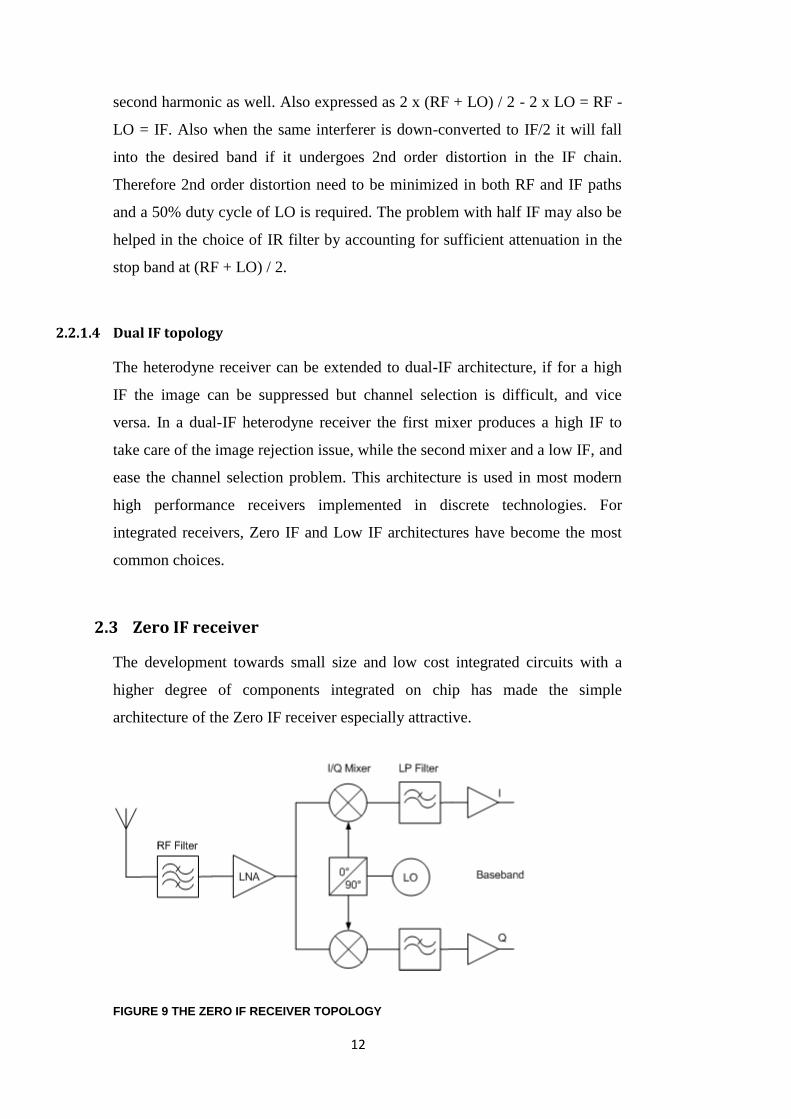
2.3 Zero IF receiver 12
2.3.1 Design considerations 13
2.3.1.1 Image rejection 13
2.3.1.2 Channel selection 15
2.3.1.3 DC-Offset 15
2.3.1.4 I/Q Mismatch 16
2.3.1.5 Even order distortion 16
2.3.1.6 Flicker noise 17
2.4 Low IF receiver 17
2.4.1 Design considerations 18
2.4.1.1 Image rejection 18
2.4.1.2 Choice of IF frequency 19
2.4.1.3 Polyphase filters 20
3 Design Outline 20
3.1 New Wireless Standards 21
3.1.1 WiMAX 21
3.1.1.1 OFDM 21
3.1.2 LTE 22
3.1.2.1 MIMO 23
3.2 Multi-standard Architectures 23
3.2.1 Introduction 23
3.2.2 Zero IF/Low IF Receiver 25
3.3 Receiver Requirements 26
3.3.1 WiMAX Specification 26
3.3.2 LTE specification 27

iv
3.3.3 AD Converter 29
3.3.4 Receiver block specification 30
4 Low noise amplifier 31
4.1 Introduction 31
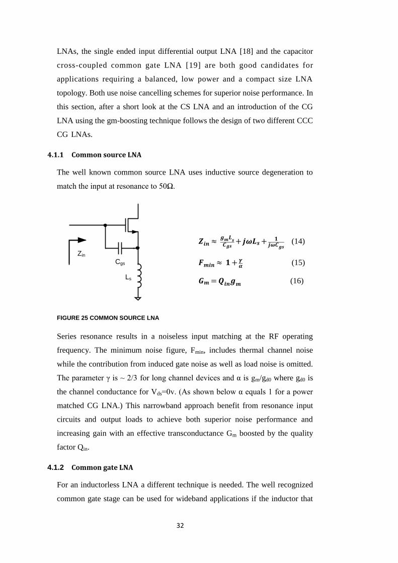
4.1.1 Common source LNA 32
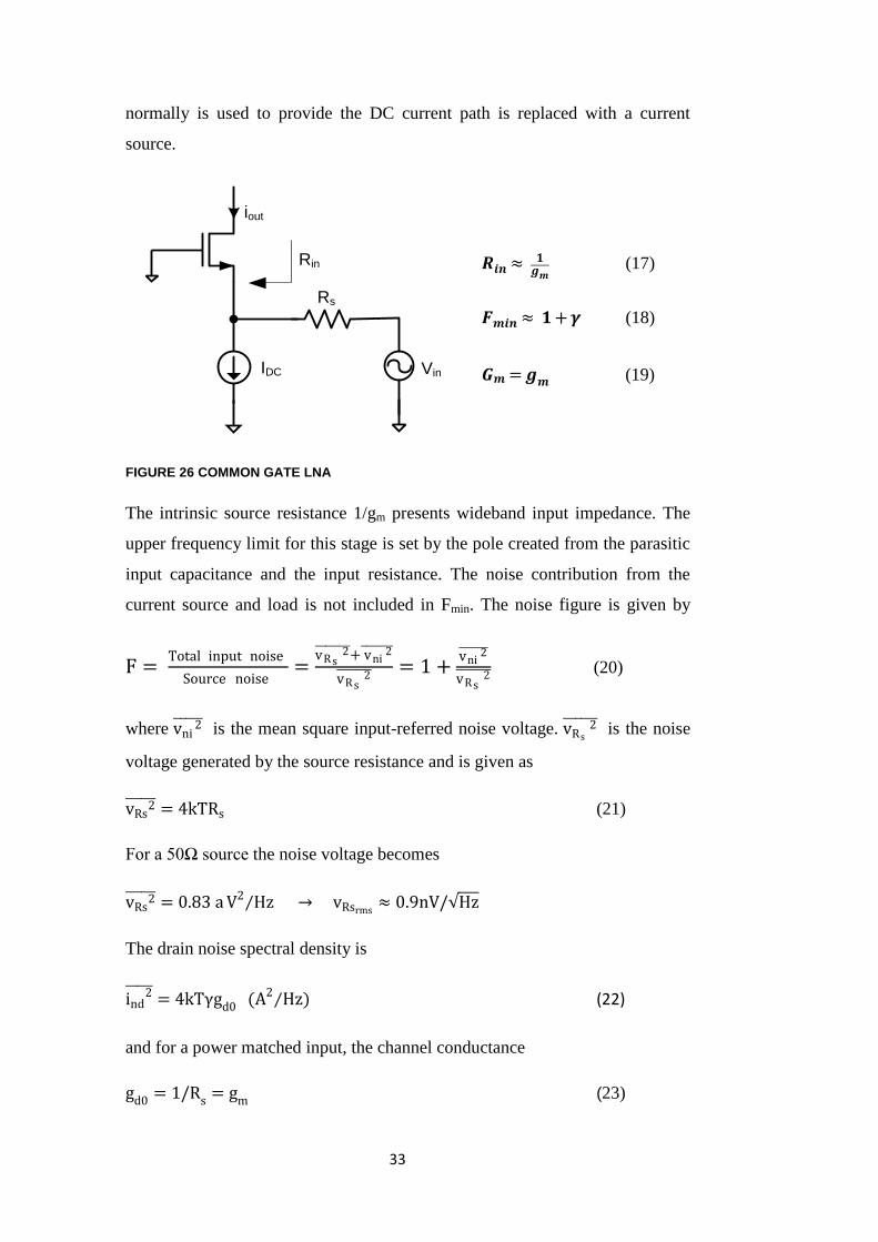
4.1.2 Common gate LNA 32
4.2 LNA design and simulation 36
4.2.1 Design 1: 2CCC CG LNA 36
4.2.1.1 Bias circuit 39
4.2.1.2 Simulation results 39
4.2.2 Design 2: OSI 2CCC CG LNA 42
4.2.2.1 Simulation results 45
4.2.2.2 Layout 47
5 Down-conversion Mixer 52
5.1 Introduction 52
5.1.1 Gilbert cell mixers 52
5.1.2 Passive mixer 57
5.2 Mixer design and simulation 59
5.2.1 Simulation results 60
5.2.2 Layout 63
6 Intermediate stages 64
6.1 Gain stage 65 6.1.1 Layout 67
6.2 Buffer 68 6.2.1 Layout 70
7 System integration 71
7.1 Simulated result 71
7.2 Layout 74
8 Conclusion 75
9 Appendix A Dual CCC CG LNA 76
10 Appendix B Bias circuit 77
11 Appendix C OSI DCCC CG LNA 78
12 Appendix D Mixer 79
13 Appendix E Gain Stage 80
14 Appendix F Buffer 81
15 Appendix F Test bench 82
16 Bibliography 83

1
1 Introduction
1.1 Project objective
A commonly used design approach for a wideband Zero IF receiver is to use
the common source LNA with either resistive feedback or LC ladder network
to achieve a wideband input match. To achieve low flicker noise as required for
a Zero IF receiver, an active Gilbert mixer with current bleeding techniques
have been used. Recent development of the common gate LNA using CCC
technique has resulted in both a lower noise figure equal to the CS LNA as
well as improved gain. These improvements together with the advantage that a
CG LNA can be implemented without bulky inductors have made it a good
choice for wideband receiver front-end. The main motivation for this work is to
perform a case study of the design methodology that takes advantage of
inductor less circuit topologies and novel design techniques such as CCC and
low flicker noise passive mixers to archive compact size and low power
receiver front-ends.
1.2 Thesis description
First in chapter 2 the radio receiver is introduced with focus on architectures
suitable for integration. In chapter 3 a brief on the 4G standards WiMAX and
LTE is followed by receiver system design. Requirements are identified and
adapted to the LNA and mixer that are described and designed in the main
chapters 4 and 5. The circuit design of this work also includes intermediate
stages in chapter 6. System results are presented in chapter 7 before a final
chapter with conclusions.
2 Receiver architectures
The function of a receiver is to successfully demodulate a desired signal in the
presence of strong interferers and noise [1]. The received signal power is a
function of distance and the surrounding environment between the transmitter
and the receiver. Reflected signals from different signal paths result in

2
multipath fading as signals add up out of phase at the receiver antenna. This
phenomenon introduces an enormous variation of the received signal level and
requires systems to have a large dynamic range. Apart from a high dynamic
range combined with the ability to reject strong interferers, a receiver system
needs to minimize cost and power consumption. Altogether a number of
different requirements translate into different receiver architectures, but the
most important for this work are treated below. Here the operation and design
of the analog front-end will be discussed, that include LNA and mixers as
shown in Figure 1. It will be presumed that the demodulation is preferably done
in a DSP after digitizing the signal at baseband.
.
FIGURE 1 SUPER HETERODYNE RECEIVER ARCHITECTURE
2.1 General considerations
2.1.1 Receiver sensitivity
In wireless communication one of the key receiver system requirements is its
sensitivity. Sensitivity is defined as the minimum signal level that a receiver
can detect with acceptable signal-to-noise-ratio. The receiver sensitivity is
expressed in dBm as
S = Prs + NF + SNR + 10logB (1)
where NF is the receiver noise figure, SNR the signal-to-noise-ratio, B the
channel bandwidth and Prs is the noise power delivered to a conjugate matched
receiver input by the source resistor Rs given as
Prs=Uin2/Rin= 4kTRs/4Rin = kT = -174 dBm/Hz (2)

3
The receiver sensitivity is illustrated in Figure 2. Here the sum of the three first
terms is the total integrated noise of the system, called the noise floor, Pnf
Pnf = -174 dBm + NF + 10logB (3)
The SNR adds up from the noise floor to the receiver sensitivity as a margin
between signal and noise.
Pin
B
Frequency
SNR
10logB
NF-174 dBm
0
Smin
FIGURE 2 RECEIVER SENSITIVITY
It is clear that low input noise is critical for detecting the weakest signal and
that highest receiver sensitivity can be achieved for narrowband channels with
low SNR. The required SNR depend on the used modulation technique and the
required bit error rate (BER).
2.1.1.1 Channel capacity
Another very important property in the receiver system that greatly depends on
bandwidth and SNR is the channel bit rate. The maximum channel capacity is
defined by the Shannon theorem as
C = B*log2 (1+SNR) (bits/s) (4)

4
The Shannon theorem states that both increasing the channel bandwidth and
SNR improves channel capacity. This obviously stands in direct contradiction
with high sensitivity and indicates that long distance transmission and high
data rate is hard to combine. One related limitation in the wireless
communication environment is the limited spectrum e.g. in urban areas.
Limited spectrum result in narrow bandwidth allocated for each user,
mandating the need for coding techniques to reach the maximum rate as
defined by Shannon.
2.1.2 Receiver selectivity
Another key characteristic of a receiver is its selectivity. Selectivity is defined
as the ability of a receiver to satisfactory extract the desired signal in presence
of strong adjacent frequency interferers and channel blockers. In most
architectures, the front-end band select filter and the channel select filter at the
intermediate frequency (IF), sets the selectivity of the receiver. The band select
filter reject out of band interferers and the channel select filter reject out of
channel interferers that are usually located in band. The difficulty with
selecting the channel directly in the front-end is demonstrated below. In this
example a hypothetical band pass filter for a 900MHz receiver selects a 30kHz
channel while rejecting interfering channels 60kHz away [2].
FIGURE 3 HYPOTHETICAL FRONT-END CHANNEL SELECT FILTER

5
For a simple second-order LC-bandpass filter, to achieve 60 dB attenuation
45kHz from the center frequency 900MHz, an equivalent Q on the order of 107
is required. This Q value is possible only for devices such as surface acoustic
wave filters (SAW). It is also important to note that typical filters exhibit a
trade-off between loss and Q value. Low loss is important since this filter is
preceding the first LNA gain stage in the receive chain. As shown by Friis
equation (5) the loss will add directly to the total noise figure without being
scaled since there is no preceding gain.
NFtot = 1 + NF1 − 1 + NF 2−1
G1+ ⋯ (5)
For these reasons only the band of interest can be selected by the front-end
filter. As a result the channel selection is done at a lower carrier frequency after
frequency translation.
2.1.2.1 Linearity
It’s also important for the selectivity that a receiver is linear and process the
signal with an acceptable distortion level. If the frequency selection and
linearity of the receiver is insufficient it can generate intermodulation products
that degrade performance. Generally, the level of distortion determines the
maximum power of an input signal that a receiver can process. Of particular
interest for many receivers is 3rd order distortion that may generate
intermodulation products close to the desired signal. An example is illustrated
in Figure 4 where inband interferers generate IM3 products that fall in the
desired channel.

6
FIGURE 4 INBAND INTERMODULATION DUE TO NONLINEARITIES IN THE RECEIVER
FRONT-END
The acceptable level of the undesired IM3 product in the desired channel is
given as
PIM3 = Pds – CCRR (dBm) (6)
where Pds is the desired signal and CCRR is the specified co-channel rejection
ratio. The linearity of the receiver is usually characterized by the third order
input intercept, IIP3. The intercept point can be calculated from a two tone
measurement and is given by
IIP3 =Pin + (Pud – PIM3)/2 (dBm) (7)
where Pud is the power of the undesired channel interferers that produce an IM3
product in the desired channel, in the same manner as with a two tone test. The
second order intercept point IIP2 and even order distortion also plays an
important role for the receiver performance as will be further described for the
Zero IF receiver.
IIP2 =Pin + (Pud – PIM2) (dBm) (8)
Similarly for a system with the input-output characteristics
vout = α1vin + α2vin2 + α3vin
3 (9)
the IIP2 and IIP3 point in power are given by

7
IIP2 = 1
2
α1
α2
2
, IIP3 = 2
3 α1
α3 (10)
Besides intermodulation, other important effects of nonlinearity are
Gain compression (2.1.2.3)
Harmonic distortion, where the output from a nonlinear system with a
single tone input generally exhibit frequency components that are
integer multiples of the input frequency.
Desensitization and blocking is an effect of third order distortion where
the desired signal is processed together with a strong interferer that
tends to reduce the gain of the desired signal. This effect is critical in
the receiver front-end because a gain drop in the LNA, as a result from
blocking, will cause the noise of the subsequent stages to raise the
overall noise figure.
Cross modulation also occur when a weak signal is processed together
with a strong interferer. If the interferer is AM modulated, third order
distortion causes spurious AM on the wanted signal.
2.1.2.2 Receiver dynamic range
The dynamic range is generally defined as the ratio between the strongest and
weakest signal a receiver is able to process with reasonable signal quality.
While the sensitivity sets the lower limit, the upper limit depends on
application. In RF design the spurious free dynamic range (SFDR) and the
blocking dynamic range (BDR) is of particular importance. The upper limit for
the SFDR is set by the maximum receiver input level in a two tone test for
which the third-order intermodulation product is below the noise floor. Based
on equations (3) and (7) the SFDR can be derived as
SFDR = 2/3 (IIP3 - Pnf) – SNR (dB) (11)
A mechanism that affects the dynamic range of the receiver is called reciprocal
mixing, Figure 5. The local oscillator contains phase noise due to random

8
deviation of the oscillator frequency. When the noise sidebands of the local
oscillator mix with strong signals, that are close in frequency to the wanted
signal, unwanted noise product are produced that add to the noise floor at the
intermediate frequency and threaten to degrade the receiver sensitivity.
FIGURE 5 RECIPROCAL MIXING
2.1.2.3 Gain compression
An important definition related to linearity and dynamic range is the 1 dB
compression point. The P1dB point quantifies the compressive or saturating
behavior of a circuit and is defined as the input signal level that cause the small
signal gain to drop 1 dB.
Pin (dBm)
Pout (dBm)
P1dB
FIGURE 6 GAIN COMPRESSION
Two useful approximations for IIP3 and BDR calculated from P1dB are
IIP3 P1dB + 10 dB (dBm) (12)

9
The blocker dynamic range is defined as the ratio of the upper bound signal
P1dB to the lower bound signal sensitivity S expressed as
BDR P1dB – S (dB) (13)
2.2 Heterodyne
The superheterodyne receiver was invented by Armstrong in 1917 and is the
most well know and used radio receiver. The simple concept of the heterodyne
receiver is to down-convert the RF band to an intermediate frequency (IF) to
relax requirements on the filter that perform channel selection. Figure 7 shows
the superheterodyne receiver dual conversion architecture used in a device
designed for 2.4GHz ISM band applications.
FIGURE 7. SUPERHETERODYNE RECEIVER ARCHITECTURE WITH QUADRATURE
DOWN-CONVERSION
The operation of this architecture and the frequency translation is well
understood by looking at the radio spectrum at some critical nodes in Figure 7
together with Figure 8. An RF filter preceding the low noise amplifier
attenuates the out of band blockers as well as the image. Here a narrow band
front-end LNA allows for high sensitivity of the receiver. The image frequency
is further attenuated to an acceptable level by using an external image reject
filter. The entire spectrum is then down-converted to a fixed intermediate
frequency using a tunable local oscillator (LO1) that covers the whole RF
band. An off-chip IF-filter selects the desired channel and filters out unwanted

10
mixing products. The IF-filter is typically a high Q SAW-filter. The second
down-conversion is usually quadrature in nature to facilitate processing of
digitally modulated in-phase (I) and quadrature (Q) signals. At baseband, LP
filters reject unwanted mixing products in I and Q paths before A to D
conversion and demodulation. The image frequency at node 3 is further
rejected when I and Q paths are summed, usually done after the A to D
conversion.
FIGURE 8 FREQUENCY DOWN CONVERSION FOR THE SUPERHETERODYNE
ARCHITECTURE
2.2.1 Design considerations
2.2.1.1 Problem of image frequency As illustrated in Figure 8 node 1, the two bands symmetrically located above and
below the LO are both down-converted to IF. The image frequency
If = 2LO – RF. The problem with image is serious since it allows two different

11
channels to be down-converted into the same channel at IF frequency. This
implies stringent requirements on image rejection. An important drawback of
the heterodyne architecture is that the image reject filter is usually an off-chip
50Ω passive filter. This also requires the LNA to drive a 50Ω input, leading to
severe trade-offs between G, NF, stability and power dissipation of the LNA.
The received image signal may also be effected by the choice of LO frequency.
To down-convert the RF band, the LO can be selected on either the high side
(RF+IF) or the low side (RF- IF) of the carrier. The selection of LO may
therefore be chosen to avoid the most noisy image band. But usually low side
injection is preferred since it results in a lower tuning range (f0/BW) of the LO
and therefore ease oscillator design. For FDD systems with high IF, the
duplexer may reject image enough so the LNA can be directly coupled to the
mixer. In the heterodyne receiver, image rejection can also be performed by the
use of image reject mixer (IRM) as first mixer. This structure improves image
signal suppression and relaxes the design of IR filters. The different methods
will be further described for Zero- and Low IF architectures.
2.2.1.2 Choice of IF frequency
The choice of IF-frequency is a trade-off between image rejection and channel
selection. Choosing a high IF will move the image further away from the RF
band and therefore reduce the required Q value of the image reject filter. But at
the same time a high IF requires a high Q for the channel select filter to reject
the adjacent channel interferers. Also critical for the choice of IF is the
increased loss in IR filter when compensating with a higher Q value for a lower
IF. Since the image degrades the sensitivity of the receiver, it can be said, the
choice of IF entails a trade-off between sensitivity and selectivity.
2.2.1.3 Problem of Half IF
The frequency located in the receive band equally spaced between the RF and
LO is of special interest in the IF receiver. An interferer at this frequency (RF +
LO) / 2, in combination with 2nd order distortion, will generate a second
harmonic that will be down-converted to IF, if the LO contain a significant
12
second harmonic as well. Also expressed as 2 x (RF + LO) / 2 - 2 x LO = RF -
LO = IF. Also when the same interferer is down-converted to IF/2 it will fall
into the desired band if it undergoes 2nd order distortion in the IF chain.
Therefore 2nd order distortion need to be minimized in both RF and IF paths
and a 50% duty cycle of LO is required. The problem with half IF may also be
helped in the choice of IR filter by accounting for sufficient attenuation in the
stop band at (RF + LO) / 2.
2.2.1.4 Dual IF topology
The heterodyne receiver can be extended to dual-IF architecture, if for a high
IF the image can be suppressed but channel selection is difficult, and vice
versa. In a dual-IF heterodyne receiver the first mixer produces a high IF to
take care of the image rejection issue, while the second mixer and a low IF, and
ease the channel selection problem. This architecture is used in most modern
high performance receivers implemented in discrete technologies. For
integrated receivers, Zero IF and Low IF architectures have become the most
common choices.
2.3 Zero IF receiver
The development towards small size and low cost integrated circuits with a
higher degree of components integrated on chip has made the simple
architecture of the Zero IF receiver especially attractive.
FIGURE 9 THE ZERO IF RECEIVER TOPOLOGY

13
In the Zero IF receiver the RF band is translated to baseband directly with an
LO equal to the input carrier frequency. The image reject filter before the
mixer is eliminated since the image frequency is zero. After quadrature down
conversion and generation of I and Q signal paths, channel selection is
performed in the LP filters before demodulation. The main advantages are that
no high Q image reject filter is required and that the IF SAW channel select
filter can be replaced with LP filters at baseband, suitable to monolithic
integration. For AM signals double sideband is required since it overlaps
positive and negative parts of the input spectrum. For frequency and phase-
modulated signals the direct down-conversion to baseband must provide
quadrature outputs so as to avoid loss of information. This is because the two
sides of FM or QPSK spectra carry different information. The Zero IF receiver
has become a good choice for systems based on digital communication e.g. like
GSM and DECT. In these systems, a lower performance can be accepted in
exchange for the higher degree of integration and the ease with which a Zero IF
receiver can be combined with a DSP for the baseband demodulation of the
digital signal [3]. As will be described in the next section, performing direct
conversion to baseband entails a number of design challenges that doesn’t exist
or is not that serious for heterodyne receivers.
2.3.1 Design considerations
2.3.1.1 Image rejection
Even though the IF frequency is zero, the down-converted signal will contain a
mirrored image of the wanted signal itself as illustrated in Figure 10 below.

14
FIGURE 10 DIRECT DOWN-CONVERSION BY MIXING THE RF SIGNAL WITH A SINGLE
SINE
Figure 10 b) show the sum and difference frequencies of +- ωc and +- ωLO,
with the wanted signal and the mirrored image superimposed on each other.
The problem with the undesired image is solved by performing the down-
conversion in quadrature, and splitting the RF signal path into I and Q paths
before channel filtering and demodulation. This multiplication of the RF signal
with a polyphase signal is an example of image rejection by down-conversion
with a single positive frequency, as shown in Figure 11 below.
FIGURE 11 DOWN-CONVERSION WITH A POSITIVE FREQUENCY.

15
Figure 11 b) show the sum and difference frequencies of +- ωc and +ωLO with
the wanted signal. In this way, only the signal situated at negative frequencies
is down-converted and therefore there is no superposition of the lower and
upper sideband at baseband. The precision with which I and Q paths can be
matched determines how good the mirrored signal can be suppressed. See
section I/Q Mismatch.
2.3.1.2 Channel selection
Rejection of out of channel interferers requires active LP filtering and exhibit
severe noise-linearity-power-trade-offs compared to passive filters. And
therefore, to optimize the performance of the baseband chain (Figure 9), the
mutual placement of the LP filter, amplifiers and ADC need to be considered.
1) With the LP filter followed by gain stage and ADC, impose severe noise-
linearity trade-offs on the filter while allowing the amplifier to be a nonlinear,
high gain amplifier and the ADC to have moderate dynamic range.
2) Placing the gain stage before the LP filter relaxes noise requirements of the
filter while the amplifier needs to have high linearity. An extra amplifier may
be needed after the filter, to overcome the noise of the ADC.
3) Channel selection in the digital domain require the ADC both to archive
high linearity so as to digitize the baseband signal with minimal
intermodulation between desired signal and interferers, and exhibit a thermal
and quantization noise floor well below the signal level.
2.3.1.3 DC-Offset
Finite isolation between the LO port and both mixer and LNA inputs cause the
LO signal to leak from the LO port to the mixer RF input. The LO leakage is
then down-converted to DC. This effect is called self-mixing and the unwanted
DC offset at the mixer output threaten to saturate the following baseband
stages. The problem with self-mixing is aggravated when the LO signal leaks
to the antenna and is then radiated and reflected back to the receiver from

16
moving objects. This cause the offset to vary in time which makes it difficult to
distinguish the desired signal from the time varying offset. For this reason Zero
IF receivers require circuitry for offset cancellation. Since many signal
spectrums exhibit an energy peak at zero frequency, the simplest method with
AC coupling capacitors at the mixer output will distort the desired signal. And
in addition to demanding unacceptable large capacitors it fails to track the fast
variation in the dc offset. Instead used techniques are DC free coding,
switching in-between TDMA bursts and cancellation by DC feedback from the
digital baseband after offset calculation in the digital domain using DSP. The
Zero IF receiver and the problem with DC-offset has been known for years and
the introduction of DSPs and the new possibilities with offset cancellation have
helped the Zero IF receiver to become a good choice for practical applications.
2.3.1.4 I/Q Mismatch
Mismatches in I and Q paths between the nominally 90° phase shift and the
amplitude of I and Q signals corrupt the signal constellation and thereby raising
the bit error. This mismatch also occurs for heterodyne receivers with I/Q
down-conversion but is more critical for the Zero IF receiver since I/Q
separation is done at much higher frequency and is therefore more sensitive to
mismatches in parasitics. The Zero IF receiver also has higher gain in the
baseband path compared to the heterodyne, where most of the signal
amplification is done before the I/Q mixer, and therefore the mismatch in gain
becomes more critical.
2.3.1.5 Even order distortion
The problem with even order distortion occur when two nearby interferers (ω1
and ω2) in the receive band, that exhibits 2nd order distortion in the LNA and
mixer, generates a low frequency beat signal (ω1 - ω2) that is fed through the
mixer due to finite isolation. Even order distortion in the receiver front-end
may also generate a low frequency signal from the desired RF signal if the RF
signal happens to be AM modulated, e.g. as a result from fading during
propagation. Because of the second order nonlinearity, the AM component will
17
then be detected from the RF signal. This effect is called AM detection. In the
same way as for the beat frequency the low frequency AM component is fed
through the mixer and corrupts the baseband signal. These effects impose
stringent requirements on IP2 performance of the LNA and mixer. In order to
suppress 2nd order distortion it is common practice to use differential
architectures in the RF front-end of Zero IF receivers. .
2.3.1.6 Flicker noise
For Zero IF receivers the flicker noise is highly critical. The signal level at the
mixer output is still relatively low after a typical gain of 30 dB in LNA and
mixer. And since the down-converted spectrum extends from zero frequency
(for both positive and negative frequencies), the flicker noise at the output of
the mixer may substantially corrupt the baseband signal. This indicates that 1/f
noise of the down-conversion mixer has to be carefully minimized for the
design of a Zero IF receiver, as will be further described in section Down-
conversion Mixer.
2.4 Low IF receiver
In the low IF receiver the RF band is down-converted to a first low
intermediate frequency, typically a few megahertz. The main advantage with
down-conversion to a low intermediate frequency instead of directly down to
zero frequency is that the problem with DC offset and flicker noise can be
avoided, and at the same time off-chip IR- and IF-filters can be eliminated.
However, as described for the heterodyne, a low IF keeps the image frequency
so close to the target frequency that suppressing the image require an
impossibly high Q of the filter preceding the mixer. The solution here is instead
to use an I/Q image reject mixer together with a low Q polyphase filter that
performs channel selection and additional image rejection before the final
down-conversion to baseband. In this way separation of the mirrored signal
from the wanted signal is postponed from the RF path to the IF path so that the
front-end IR filter can be removed. The low IF receiver is well suited for high
integration just as the Zero IF receiver. The former typically has better

18
performance but, as will be described below, a more complex and power
consuming baseband. A typical application for the low IF receiver is e.g. the
Bluetooth receiver. In Bluetooth GFSK signaling is used which has a spectrum
with considerable energy at zero frequency. And therefore the Low IF is
preferred here since dc offset and flicker noise of the Zero IF may significantly
degrade the receiver performance.
FIGURE 12 LOW IF RECEIVER TOPOLOGY USING POLYPHASE BP FILTERS
2.4.1 Design considerations
2.4.1.1 Image rejection
In the same manner as for the Zero IF receiver, the RF signal is down-
converted with a quadrature mixer but with an LO slightly lower (or higher)
than the carrier frequency.
FIGURE 13 DOWN-CONVERSION TO A LOW IF WITH A POSITIVE LO FREQUENCY.

19
Both the wanted and the mirror signal are down-converted to IF frequency but
without being superimposed on each other. From Figure 13 b) it is clear that a
complex negative pass filter (NPF) in combination with the quadrature down-
converter (here with a low side injection LO) will reject the image and pass the
wanted signal [4]. One disadvantage with the low IF architecture is that the
image rejection need to be higher compared to the Zero IF receiver. For the
latter, the mirrored signal will have the same power level as the wanted signal,
while the former, the image signal can be much higher than the wanted signal.
This means that for a high quality Zero IF receiver, an image suppression of 40
dB results in an SNR of 40 dB for the wanted signal. For the low IF 70 dB
suppression is required for a SNR of 40 dB when the mirrored signal can be 30
dB higher than the wanted signal. See also section Choice of IF frequency. Again,
the precision in the matching between the two signal paths are crucial for
effective image suppression and a low bit error rate.
2.4.1.2 Choice of IF frequency
The choice of IF is a trade-off between selectivity and sensitivity as also
described for heterodyne. Typically IF is chosen as low as possible to relax
required Q of the polyphase filter, but at the same time positioning the IF so
that the lower limit of the channel bandwidth is well above the flicker noise
corner to avoid distortion from low frequency noise. The IF may also be
chosen so that the mirror frequency is situated between two transmission
channels [5] as illustrated in Figure 14. In this way suppression specs can be
lowered possibly 10-20 dB for a low IF receiver.
FIGURE 14 CHOICE OF IF TO REDUCE IMAGE NOISE

20
2.4.1.3 Polyphase filters
Instead of two separate BP filters for channel selection the low IF benefits from
using one polyphase filter. The polyphase filter acts as an all pass filter for
negative frequencies and a band stop filter for positive frequencies, or vice
versa, as also described in section Image rejection . This filter can be entirely
passive, built of only resistors and capacitors. An implementation more suitable
for integration is the active filter Figure 15. The disadvantages with the
polyphase filter are mainly its sensitivity to mismatch that reduces image
suppression and the increased power consumption for wideband channel
applications when this filter topology is used [6]. The latter property makes the
low IF receivers more suitable for narrowband channel system like e.g. GSM
or Bluetooth where the channel BW is 200 kHz and 1 MHz respectively.
A1
A2
From I/Q Mixer
-1
I
Q
FIGURE 15 ACTIVE POLYPHASE FILTER STAGE
3 Design Outline
This chapter both describes the new radio standards and the receiver
architecture that applies to this work and identifies the requirements it impose
on the LNA and mixer to be designed. .

21
3.1 New Wireless Standards
Although 3G technologies deliver significantly higher bit rates than 2G
technologies there is still the ever increasing demand for “wireless broadband”,
lower latency1, and multi-megabit throughput. LTE and WiMAX among others
provide new technologies to meet this demand for connectivity from new
generations of consumer devices tailored to new mobile applications. Figure 16
below illustrates current standards for mobile and data communication.
FIGURE 16 STANDARD OVERVIEW [7]
3.1.1 WiMAX
WiMAX IEEE 802.16e is a new wireless standard for mobile broadband and is
intended to provide high bandwidth voice and data for residential and
enterprise. Providing higher data rates and longer reach, WiMAX is a possible
replacement candidate for cellular phone technologies such as GSM and
CDMA/UMTS, or can be used as a layover to increase capacity. With mobile
WiMAX, there is an increasing focus on portable subscriber units. This
includes handsets, PDAs, PC peripherals and other consumer electronic
devices.
3.1.1.1 OFDM
The modulation used in WiMAX to achieve these high data rates is orthogonal
frequency-division multiplexing. A WiMAX OFDM signal shown in Figure 17
features a minimum of 256 subcarriers up to 2048 subcarriers, each modulated
1 Latency is the delay between requesting data and getting a response

22
with BPSK, QPSK, 16 QAM or 64 QAM. Having these carriers orthogonal to
each other minimizes self-interference. This standard also supports different
signal bandwidths. The composite signal envelope amplitude of the OFDM
signal can exhibit significant peaks and valleys. Theoretically, there is a
possibility that the signals on each individual carrier reach their peaks at the
same time, contributing to a peak-to-average power ratio (PAPR) e.g. for
WiMAX 256-OFDM of about 12 dB. This imposes significant constraints on
transmitter/receiver linearity and requires large power back-off.
FIGURE 17 BASEBAND SPECTRUM OF WIMAX OFDM 20MHZ CHANNEL SIGNAL[14]
3.1.2 LTE
LTE (3GPP Long term evolution) is together with WiMAX the major
competing technology in the development of mobile broadband for the fourth
generation networks [8]. LTE will be available not only in next-generation
mobile phones but also in notebooks, ultra-portables, cameras, camcorders,
Fixed Wireless Terminals and other devices that benefit from mobile
broadband. Specific technical requirements include
High throughput. LTE is expected to deliver three to five times greater
capacity than the most advanced 3G networks.
Low latency. Reduced latency time will enhance the behavior of time
sensitive applications (VoIP).
Flexible carrier bandwidths from 1.4 to 20MHz for both TDD and FDD
Two key enabling technologies important to help meeting performance
objectives both for LTE and WiMAX are MIMO (Multiple input/Multiple
output) and the already mentioned OFDM.
23
3.1.2.1 MIMO
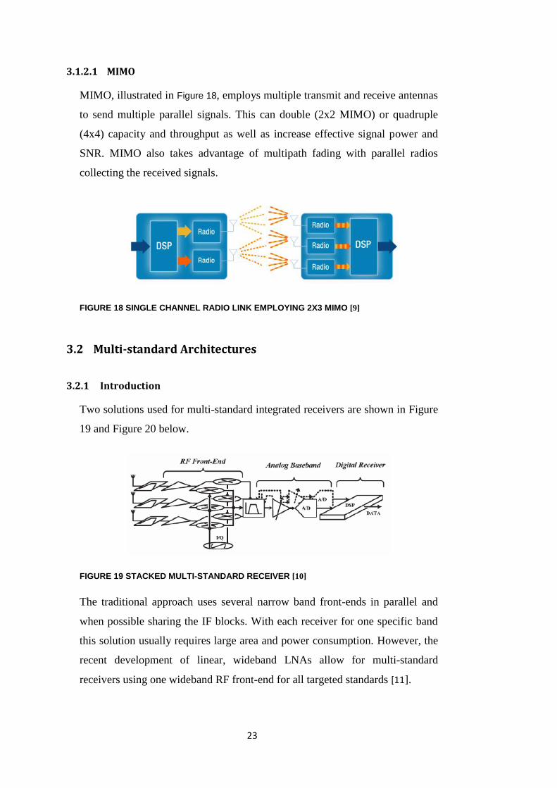
MIMO, illustrated in Figure 18, employs multiple transmit and receive antennas
to send multiple parallel signals. This can double (2x2 MIMO) or quadruple
(4x4) capacity and throughput as well as increase effective signal power and
SNR. MIMO also takes advantage of multipath fading with parallel radios
collecting the received signals.
.
FIGURE 18 SINGLE CHANNEL RADIO LINK EMPLOYING 2X3 MIMO [9]
3.2 Multi-standard Architectures
3.2.1 Introduction
Two solutions used for multi-standard integrated receivers are shown in Figure
19 and Figure 20 below.
FIGURE 19 STACKED MULTI-STANDARD RECEIVER [10]
The traditional approach uses several narrow band front-ends in parallel and
when possible sharing the IF blocks. With each receiver for one specific band
this solution usually requires large area and power consumption. However, the
recent development of linear, wideband LNAs allow for multi-standard
receivers using one wideband RF front-end for all targeted standards [11].

24
Tx/Rx
Tx
Duplex
Tx
Duplex
Tx Wideband
LNA
Lb
ChipBoard
Figure 20 Multi-standard receiver front-end
The wideband LNA is combined with a section for different multiple access
techniques. With the development of wireless systems into multi-standard
receivers, this section becomes increasingly complex since it must both support
different frequency bands as well as different duplexing techniques of the
targeted standards. Therefore this section takes a large part of the total cost of
the RF front-end and takes up large space since it is normally designed off-chip
if it’s not available as a front-end module (FEM). In the simplified example
above the LNA is preceded by a Tx/Rx switch and duplex filters to support
both TDD and two bands with FDD. The insertion loss in the switches and
duplexer preceding the LNA is critical since the loss will add directly to the
total noise figure. The LNA also need to have good noise performance as well
as low input return loss over the whole frequency range that covers the targeted
standards. A Zero IF front-end that use differential signaling (to minimize
second order distortion) will benefit from using duplex filters with differential
outputs to avoid extra loss in an off-chip balun. A bonding wire inductance Lb
indicates the PCB and chip interface. .
Freq (GHz)
GSM WiMAXWiMAX WiMAXPCS IMT-E
0.9 1.9 2.5 2.6 3.5 5.8
Figure 21 WiMAX frequency bands and some of the UMTS bands designated for LTE

25
3.2.2 Zero IF/Low IF Receiver
As described in Receiver architectures the most suitable architectures for high
integration, small size and low power radio front-ends are the Zero IF and the
Low IF receivers. The Low IF avoids the well known issues with flicker noise
and DC offset for the Zero IF. This comes at the expense of a more complex
and power consuming baseband. The choice of Zero IF or Low IF depends
mainly on the signal that will be processed. A narrow band signal that is down-
converted to Zero IF will contain a substantial part of the total power close to
DC. The removal of DC offset required for Zero IF by either AC coupling, a
notch filter or a DC cancellation loop will therefore result in signal
degradation. Also flicker noise will have a larger impact on total integrated
channel noise for a narrow band channel centered at zero frequency. Therefore
narrow channel bandwidths used in GSM may require a Low IF receiver while
a Zero IF can be used for the wider channels in WiMAX and LTE. As a result,
a wideband radio architecture supporting LTE and WiMAX can have identical
RF front-ends while the baseband may be either implemented as a Zero IF or
Low IF. .
0°
90°LO LNA
I/Q Mixer
VGA
VGA
CT Σ∆ LP AD Converter
DSP
I
Q CT Σ∆ LP AD Converter
FIGURE 22 ZERO IF RECEIVER INCLUDING AD CONVERTER
The front-end uses a wideband LNA together with an I/Q mixer. A passive
mixer is here required to minimize 1/f noise. The variable gain amplifier
(VGA) as first IF stage improves the relatively low front-end gain. Passive LP
channel select filters as well as anti-alias filtering are embedded in the ADC.
See section AD Converter. The Low IF version of this architecture uses a
complex BP filter (Figure 15) for channel selection instead of a LP filter. This
BP filter also has the task of rejecting the image frequency.

26
Design issue: The VGA is required to have high linearity and low 1/f-noise as
well as low power consumption. This may impact the power consumption for
the Low IF since the increased gain bandwidth product will result in increased
power consumption. Therefore the receiver may benefit from increasing the
front-end gain to relax the requirements on the VGA. .
3.3 Receiver Requirements
This section summarizes the requirements that a receiver should achieve in
order to comply with the WiMAX/LTE 4G standards [12], [13]. Since the LTE
standard is not yet clearly defined, the LTE requirements are here identified by
looking at well established standards such as GSM and UMTS that the LTE
user equipment need to coexist with. After the system level study, the achieved
specifications are translated to each receiver block including the LNA and
mixer circuits that are to be designed. The used approach to determine the
block requirements can be divided in four steps
1. Identifying the receiver system requirements based on the targeted
standards
2. Literature study of CMOS high performance sigma-delta ADC to
identify realistic performance for this application
3. Determine receiver total gain based on 1 and 2
4. Link budget to extract system requirements on LNA and mixer blocks
3.3.1 WiMAX Specification
TABLE 1 WIMAX SIGNAL CHARACTERISTICS
Modulation OFMDA (QPSK/16QAM/64QAM)
Duplex TDD / H-FDD
Channel bandwidth 1.5 – 28MHz
SNRmin (QPSK1/2) 5 dB
Bit rate 10 – 70 Mbps

27
Spectral efficiency 3.7 bit/s/Hz
Maximum input signal -30 dBm
The minimum sensitivity Smin becomes -99 dBm for QPSK at bandwidth
1.5MHz as defined in section Receiver sensitivity. Since the received signal can
be as weak as -99 dBm the receiver need to have large gain to overcome the
ADC input noise floor. The high gain in combination with maximum received
signal will impose extremely high linearity in the last stages. To avoid this, the
gain is divided into two modes as shown in Figure 24. In the high gain mode the
IIP3 requirements are determined by intermodulation test with an interfering
signal to -16 dBm. For the low gain mode the maximum received signal -30
dBm requires a receiver input P1db of -18 dBm when accounting for the needed
12 dB back-off (PAPR). This sets IIP3 in the low gain mode to -8 dBm as
defined in section Gain compression . A non adjacent channel rejection test
determines IIP2 for the receiver. The noise figure is set by the standard to 8 dB
[14].
TABLE 2 WIMAX RECEIVER SPECIFICATIONS
Sensitivity -99 dBm
Noise figure 8 dB
IIP3_high_gain_mode -16 dBm
IIP3_low_gain_mode -8 dBm
IIP2 +25 dBm
3.3.2 LTE specification
TABLE 3 LTE SIGNAL CHARACTERISTICS
Modulation downlink OFMDA (QPSK/16QAM/64QAM)
Modulation uplink SC-FDMA
Duplex TDD / FDD / H-FDD
Channel bandwidth 1.4 – 20MHz
SNRmin (QPSK) 0 dB
Bit rate 100 Mbps

28
Spectral efficiency 5 bit/s/Hz
Maximum input signal -25 dBm
The maximum input signal -25 dBm sets the input P1db to around -13 dBm
(accounting for PAPR as above) and therefore the required IIP3 is -3 dBm. In
the TDD mode the transmit signal leakage to the receiver input is around -20
dBm with the maximum output signal 30 dBm (1W Class 1) and a typical
Tx/Rx switch isolation of 50 dB. This condition sets out of band IIP3 to -5
dBm assuming 5 dB PAPR for the uplink SC-FDMA signal. The standard
proposes the noise figure to be 9 dB. .
TABLE 4 LTE RECEIVER SPECIFICATIONS
Sensitivity (QPSK /BW1.4MHz) -104 dBm
Noise figure 9 dB
IIP3_in_band -3 dBm
IIP3_out_of_band -5 dBm
GSM
TABLE 5 GSM SIGNAL CHARACTERISTICS
Modulation G-MSK
Duplex TDD
Channel bandwidth 200kHz
Bit rate 270kb/s
Spectral efficiency 1.3 bit/s/Hz
Sensitivity -102 dBm
TABLE 6 GSM RECEIVER SPECIFICATIONS
Noise figure 12 dB
IIP3 -18 dBm
IIP2 +49 dBm
29
WCDMA/UMTS
TABLE 7 UMTS SIGNAL CHARACTERISTICS
Modulation CDMA+QPSK
Duplex FDD
Channel bandwidth 5MHz
Bit rate 8 – 384 kBps
TABLE 8 UMTS RECEIVER SPECIFICATIONS
Noise figure 6 – 7 dB
IIP3_in_band -17 dBm
IIP3_out_of_band -4.5 dBm
IIP2 +46 dBm
3.3.3 AD Converter
The conventional analog to digital converter used for wireless receivers is the
pipelined ADC. This ADC uses an analog anti-alias filter (AAF) and has
difficulty to meet the required accuracy of >10 bits for reduced supply voltage.
The discrete time sigma delta ADC can operate at low supply voltage but also
need an analog AAF because of the sampled nature of the circuit and is usually
limited to bandwidths below 2MHz. Both architectures have degraded signal to
noise ratio because the sampled-data analog circuits will alias wideband noise
into the signal bandwidth. A more suitable ADC for demanding low power
applications is the continuous time sigma delta ADC. The CT Σ∆ ADC avoids
a power-hungry AAF and noise aliasing by using a continuous time loop filter.
The non-sampled CT Σ∆ circuit also makes the ADC less susceptible to high-
frequency noise pickup, for example substrate noise generated by digital
circuits.
There are a number of Σ∆ ADCs reported in the literature. For the budget study
of this receiver a CT Σ∆ LP ADC implemented in 90 nm CMOS is chosen. The
ADC block diagram is shown in Figure 23 below.

30
FIGURE 23 CONTINUOUS TIME Σ∆ LP ADC [15]
Of interest for the Zero IF receiver line up (Figure 22) is that the architecture
includes a single pole LP filter and a third order loop filter that can be used for
baseband channel select filtering. The filter order, over sampling ratio and
number of quantization steps can be varied to keep the same signal-to-noise-
and-distortion-ratio (SNDR). The configurable architecture allows for various
signal bandwidths which makes it suitable for multi-band applications. The
ADC provides a SNDR of 61 dB with a full scale input signal of 0 dBm in a
10MHz bandwidth. The power consumption 31 mW per channel allow for
mobile applications.
3.3.4 Receiver block specification
Based on the above study of the target standards and ADC performance,
follows a level diagram to determine receiver total gain. A link budget is set up
to extract LNA and mixer requirements.

31
Full scale 0 dBm
SNRmin
5 dB
Smin -99 dBm
Smax -25 dBm
Ghigh 35 dB
Glow 13 dB
DR 74 dB
PAPR 12 dB
SNDR 69 dB
BW 1.5 MHz
Noise floor
-69 dBm
FIGURE 24 GAIN REQUIREMENTS FOR WIMAX/LTE RECEIVER
TABLE 9 RECEIVER LINK BUDGET
Switch/
Duplexer LNA Mixer VGA
Cascaded
performance
Receiver
specification
Gain (db) -2 25 -2 14 35 35
NF (dB) 2 5 13 7 7.2 8
IIP3 (dBm) ∞ -10 10 15 -17 -3
The link budget NF, G and IIP3 values for each block are based on state of the
art literature and what is realistic for this work in order to meet the receiver
specification. The LNA block specification includes intermediate gain stage
and mixer driver. It is clear from the IIP3 budget that the stringent linearity
requirements would require additional circuit linearization techniques in order
to meet specification.
4 Low noise amplifier
4.1 Introduction
Several LNA topologies have been demonstrated for wideband applications.
These include the conventional distributed and resistive feedback amplifiers
[16] as well as the inductively degenerated common source (CS) amplifier
using LC ladder filter [17] to achieve a wideband input match. These LNAs are
usually either power hungry or use bulky inductors. Among inductorless
32
LNAs, the single ended input differential output LNA [18] and the capacitor
cross-coupled common gate LNA [19] are both good candidates for
applications requiring a balanced, low power and a compact size LNA
topology. Both use noise cancelling schemes for superior noise performance. In
this section, after a short look at the CS LNA and an introduction of the CG
LNA using the gm-boosting technique follows the design of two different CCC
CG LNAs. .
4.1.1 Common source LNA
The well known common source LNA uses inductive source degeneration to
match the input at resonance to 50Ω.
Zin
Cgs
Ls
FIGURE 25 COMMON SOURCE LNA
Series resonance results in a noiseless input matching at the RF operating
frequency. The minimum noise figure, Fmin, includes thermal channel noise
while the contribution from induced gate noise as well as load noise is omitted.
The parameter γ is ~ 2/3 for long channel devices and α is gm/gd0 where gd0 is
the channel conductance for Vds=0v. (As shown below α equals 1 for a power
matched CG LNA.) This narrowband approach benefit from resonance input
circuits and output loads to achieve both superior noise performance and
increasing gain with an effective transconductance Gm boosted by the quality
factor Qin.
4.1.2 Common gate LNA
For an inductorless LNA a different technique is needed. The well recognized
common gate stage can be used for wideband applications if the inductor that
𝒁𝒊𝒏 ≈ 𝒈𝒎𝑳𝒔𝑪𝒈𝒔
+ 𝒋𝝎𝑳𝒔 + 𝟏𝒋𝝎𝑪𝒈𝒔
(14)
𝑭𝒎𝒊𝒏 ≈ 𝟏 + 𝜸𝜶 (15)
𝑮𝒎 = 𝑸𝒊𝒏𝒈𝒎 (16)
𝐺𝑚 = 𝑄𝑖𝑛𝑔𝑚
33
normally is used to provide the DC current path is replaced with a current
source.
iout
Vin
Rs
Rin
IDC
FIGURE 26 COMMON GATE LNA
The intrinsic source resistance 1/gm presents wideband input impedance. The
upper frequency limit for this stage is set by the pole created from the parasitic
input capacitance and the input resistance. The noise contribution from the
current source and load is not included in Fmin. The noise figure is given by
F = Total input noise
Source noise=
vR s 2 + vni
2
vR s 2 = 1 +
vni2
vR s 2 (20)
where vni2 is the mean square input-referred noise voltage. vRs
2 is the noise
voltage generated by the source resistance and is given as
vRs2 = 4kTRs (21)
For a 50Ω source the noise voltage becomes
vRs2 = 0.83 a V2 Hz → vRsrms
≈ 0.9nV/ Hz
The drain noise spectral density is
ind2 = 4kTγgd0 (A2 Hz ) (22)
and for a power matched input, the channel conductance
gd0 = 1/Rs = gm (23)
𝑹𝒊𝒏 ≈ 𝟏𝒈𝒎
(17)
𝑭𝒎𝒊𝒏 ≈ 𝟏 + 𝜸 (18)
𝑮𝒎 = 𝒈𝒎 (19)

34
The input referred noise voltage is
vni2 =
ind2
gm2 =
4kTγgm
gm2 = 4kTγRs (24)
Substituting (21) and (24) into (20) gives the noise figure as
F = 1 +Vni
2
VR s 2 = 1 +
4kTγRs
4kT Rs= 1 + γ (25)
This noise figure includes thermal channel noise only. Flicker noise and
usually also gate noise for the CG LNA is unimportant at RF, while hot
electron effects may raise the noise figure [20]. One property that also might
degrade noise performance is the low current gain of the CG LNA in
combination with a low load resistance.
iin =v in
R in= gm vin (26)
iout = gm vin → current gain one (27)
The resistor noise current is
iRs rms=
4kT
Rs (A/ Hz) (28)
Unity current gain does not scale the load noise current when referred to the
input. As a result both gain and noise figure of the CG LNA benefit from a
large load resistance. Even though the CG LNA have both superior input
matching and also linearity2, its use have been limited due to the relatively low
gain and higher noise figure, which is usually larger than 3 dB for short
channel MOSFETs devices. To overcome these disadvantages, a gm-boosting
technique [21] have been used that have made the CG LNA a good choice for
wideband applications such as mobile broadband where low power
consumption and compact size are important. The general gm-boosting
technique used in the common gate stage use a feedback loop wherein
inverting amplification is introduced between the source and gate terminals.
2 The input source impedance provides RSD in the CG topology (see also Gain stage)
35
-AVn
Vg
in+
IDC
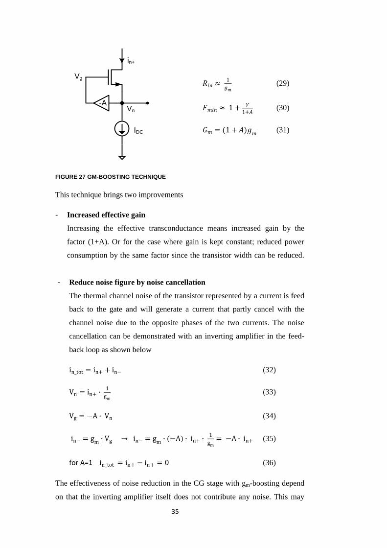
FIGURE 27 GM-BOOSTING TECHNIQUE
This technique brings two improvements
- Increased effective gain
Increasing the effective transconductance means increased gain by the
factor (1+A). Or for the case where gain is kept constant; reduced power
consumption by the same factor since the transistor width can be reduced.
- Reduce noise figure by noise cancellation
The thermal channel noise of the transistor represented by a current is feed
back to the gate and will generate a current that partly cancel with the
channel noise due to the opposite phases of the two currents. The noise
cancellation can be demonstrated with an inverting amplifier in the feed-
back loop as shown below
in_tot = in+ + in− (32)
Vn = in+ ∙ 1
gm (33)
Vg = −A ∙ Vn (34)
in− = gm ∙ Vg → in− = gm ∙ −A ∙ in+ ∙ 1
gm= −A ∙ in+ (35)
for A=1 in_tot = in+ − in+ = 0 (36)
The effectiveness of noise reduction in the CG stage with gm-boosting depend
on that the inverting amplifier itself does not contribute any noise. This may
𝑅𝑖𝑛 ≈ 1
𝑔𝑚 (29)
𝐹𝑚𝑖𝑛 ≈ 1 +𝛾
1+𝐴 (30)
𝐺𝑚 = (1 + 𝐴)𝑔𝑚
(31)

36
motivate a passive implementation of A. The differential CG stage allows for
passive inverting amplification by capacitive cross-coupling.
Vin-Vin+
CcCc
M1 M2
IDCIDC
FIGURE 28 CAPACITOR CROSS-COUPLED CG LNA
In this topology the coupling capacitor is chosen much larger than the parasitic
gate capacitance so that the voltage division ratio between the two reactances
sets A to be maximally one. With the full differential voltage swing across
each gate-source, the effective gain is doubled compared to the conventional
differential CG amplifier where the input voltage is shared between two gates.
In a similar manner as described above, the thermal noise current of each
transistor is self canceled by appearing in antiphase across the output.
4.2 LNA design and simulation
In this section design and simulation results from two versions of the CCC CG
LNA are presented.
4.2.1 Design 1: 2CCC CG LNA
The CCC CG LNA presented above has been further developed for wideband
applications.
𝑅𝑖𝑛 ≈ 1
𝑔𝑚1 (37)
𝐹 ≈ 1 +𝛾
2 (38)
𝐺𝑚 = 2𝑔𝑚1 (39)

37
Vdd
M1 M2
M3 M4
M5 M6
Vb1 Vb2
Vb3 Vb4
Vout-Vout+
RL RL
Cc
Cc
Cc
Rin
VinRs Rs
Cc
FIGURE 29 DUAL CCC COMMON GATE LNA (2CCC CG LNA)
In above topology both the input pair (M1, M2) and the current sources (M3,
M4) are cross coupled. Cascodes (M5, M6) are added to improve backward
isolation and minimize the Miller effect as to reduce the input capacitance. By
including the current sources in the cross coupling scheme the noise figure is
reduced, despite the extra noise contribution from M3 and M4. The input
resistance and noise figure for this circuit is given by
Rin = 2
2gm 1−gm 3 (40)
Fmin = 1 + γ(2 3 − 3) ≈ 1 + 0.46γ for gm1Rs = 1/ 3 (41)
The noise figure is based on thermal noise contributed by M1-M4 which makes
it comparable to previous LNA circuits above. The cascodes (M5, M6) does
usually not degrade the noise figure since its noise current will partly cancel
due to the large input resistance at the drain of M1 and M2. The condition for

38
minimum noise figure sets gm1 ~11.55mS for a 50Ω source resistance. With a
power matched input resistance of 100Ω, gm3 is 3.1mS. At this condition the
current sources contribute half the output noise of the input pair. In this
example gm1 is slightly higher than for the CCC CG where 10mS sets the input
resistance to 100Ω. Therefore gain is slightly higher for this circuit. The
voltage gain is given by
Av ≈ 2gm 1RL
1+jωCd 5RL (42)
where Cd5 is the total capacitance at the drain of M5. Thus, the low frequency
gain is ~2gm1 RL which is the same as for the CCC CG in Figure 28. The upper
frequency is limited by the output pole. In the small example above the
transconductance is chosen to achieve a perfect input match and minimum
noise figure. The design approach used for the 2CCC CG LNA simulated
below is instead to allow a certain degree of mismatch so that transistor sizes
can be minimized, resulting in reduced power consumption and improved
bandwidth. Reducing the transistor gate width will reduce gm and allow Rin to
increase to maximally 200Ω so that input return loss is kept below -10 dB. As a
result power consumption is reduced since both gm and Ids are directly
proportional to the gate width. Minimized parasitic capacitances improve
bandwidth by pushing out the output pole created by RL and Cd5. The
resonance frequency between the input parasitic capacitance and the bonding
wire inductance that threaten to degrade the input matching is also increased.
This approach may still be used to achieve minimum noise figure. However the
total noise figure largely depends on the noise contribution from the load
resistance (Figure 31). The load resistance may also be increased because of the
improved DC headroom resulting from the reduced Ids.
Based on equation (41) and for a bias current (Ids) 0.8mA, the transconductance
is 12.3 mS and 4.3 mS and the gate widths 32µm and 24µm for transistor M1
and M3 respectively. The load resistance RL is 560Ω.
39
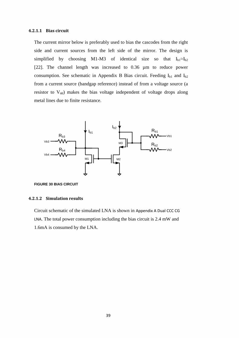
4.2.1.1 Bias circuit
The current mirror below is preferably used to bias the cascodes from the right
side and current sources from the left side of the mirror. The design is
simplified by choosing M1-M3 of identical size so that Ib1≈Ib2
[22]. The channel length was increased to 0.36 µm to reduce power
consumption. See schematic in Appendix B Bias circuit. Feeding Ib1 and Ib2
from a current source (bandgap reference) instead of from a voltage source (a
resistor to Vdd) makes the bias voltage independent of voltage drops along
metal lines due to finite resistance. .
Ib1
Ib2
M1 M2
M3
Vb1
Vb2
Vb3
Vb4
Rb3
Rb4
Rb1
Rb2
FIGURE 30 BIAS CIRCUIT
4.2.1.2 Simulation results
Circuit schematic of the simulated LNA is shown in Appendix A Dual CCC CG
LNA. The total power consumption including the bias circuit is 2.4 mW and
1.6mA is consumed by the LNA.

40
FIGURE 31 NOISE FIGURE VS LOAD RESITANCE
NFmin is 1.6 dB determined without load noise. The contribution from the load
is 1 dB to the total noise figure for RL 560Ω. The simulation is done at 2GHz
without bias net and IC passives.
FIGURE 32 INPUT RETURN LOSS
The simulated input resistance is 155Ω resulting in -13dB insertion loss. The
minimum at 3.5GHz result from the resonance between the LNA input
capacitance and a 1.5 nH bonding wire inductance (Lb) used in the simulation.
400 600 800 1000 1200 1400 1600 1800200 2000
0.5
1.0
1.5
2.0
2.5
3.0
3.5
0.0
4.0
RL (ohm)
NF
(d
B)
Noise figure vs load resistance
NFmin
IRL at 6 GHz
-11.403
IRL at 1 GHz
-13.297
1E91E8 1E10
-15
-10
-5
-20
0
freq, Hz
s11
(d
B)
Input returnloss,IRL
41
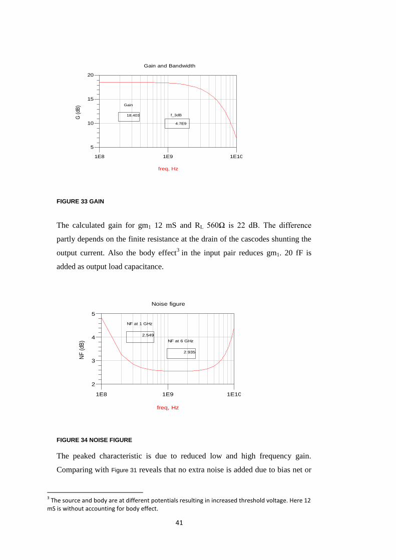
FIGURE 33 GAIN
The calculated gain for gm1 12 mS and RL 560Ω is 22 dB. The difference
partly depends on the finite resistance at the drain of the cascodes shunting the
output current. Also the body effect3 in the input pair reduces gm1. 20 fF is
added as output load capacitance.
FIGURE 34 NOISE FIGURE
The peaked characteristic is due to reduced low and high frequency gain.
Comparing with Figure 31 reveals that no extra noise is added due to bias net or
3 The source and body are at different potentials resulting in increased threshold voltage. Here 12
mS is without accounting for body effect.
1E91E8 1E10
10
15
5
20
freq, Hz
G (
dB)
Gain and Bandwidth
Gain
18.403 f_3dB
4.7E9
1E91E8 1E10
3
4
2
5
freq, Hz
NF
(dB
)
Noise figure
NF at 1 GHz
2.549
NF at 6 GHz
2.935

42
IC passives. NF is determined with s-parameter simulation, a 50 ohm source
and infinite load to avoid nose contribution to the LNA output.
FIGURE 35 IIP3 VS FREQUENCY
A swept frequency two tone test with 20MHz spacing is used to simulate the
intercept point based on the modified IIP3 equation in section Linearity as
IIP3 =Pin_dBm + (Vout_dB – VIM3_dB)/2 (dBm) (43)
Simulation is run with large input power back-off to avoid signal compression
that may produce misleading IIP3 results. The IIP2 is tested after the layout
since 2nd
order distortion in balanced circuits largely depends on mismatch.
4.2.2 Design 2: OSI 2CCC CG LNA
The stacked topology of the 2CCC CG LNA, that include RL, cascodes and
current sources result in limited DC headroom with Vds ca 250 mV on each
transistor and therefore degrading linearity. For the second design an open
source input CG LNA that has shown high linearity is chosen [23].
2E9 3E9 4E9 5E91E9 6E9
-2.0
-1.5
-1.0
-2.5
-0.5
Input frequency (Hz)
IIP
3 (d
Bm
)Linearity 2CCC CG LNA

43
Vdd
M3 M4Vb1 Vb2
M1 M2Vb3 Vb4
Rs
Vin-Vin+
Vin
Ibias
Vout-Vout+
Ibias
RL
C1 C2
C3 C4
On-chip
Off-chip
Rin
FIGURE 36 OPEN SOURCE INPUT CCC COMMON GATE LNA
The architecture above is biased from an open source input (OSI) so that the
current sources can be removed. Also cascodes are removed since reverse
isolation from the mixer LO port to LNA input is assumed enough because of
intermediate stages. The input pair M1 and M2 works in parallel with a PMOS
pair over the output load and thereby avoiding reduced DC headroom over RL.
The LNA uses dual cross coupling technique for gm-boosting and thermal noise
reduction similar to as described in section Common gate LNA. The
implementation of this simple structure benefit from a reduced number of
passive components while the biasing require an off-chip duplex-filter with a
center tapped secondary that can provide a DC-path to ground4. The input
resistance of this LNA is given as
4 Of-chip RF chokes may be used as an alternative to provide a DC path to ground

44
Rin ≈1
gm1 1 +
RL
2rds1 (44)
where rds1 is the drain-source resistance of M1. In the previous LNA design this
expression simplifies to 1/gm1 since RL is replaces with the input resistance 2/gm
of the cascode pair. But here both rds1 and RL need to be included when matching
the input pair to the source. A simplified analysis show that the gain is
Av ≈ (2gm1 + gm3)RL
2 (45)
which is the same as for the 2CCC CG LNA without gm3. While the gain
benefit from the transconductance of the PMOS pair, only moderate values of
gm3 can be allowed since increasing transconductance by choosing a larger
gate width will limit the bandwidth from the parasitic capacitance adding to the
output pole. The same design approach (with allowed mismatch) as in design 1
was used for the simulated circuit below. With Ids 0.6mA the transconductance
is 7.3 mS and 0.8 mS and the gate widths 32µm and 24µm for transistor M1
and M3 respectively. The differential load resistance RL is 1400Ω.

45
4.2.2.1 Simulation results
Circuit schematic of the simulated LNA is shown in Appendix C OSI DCCC CG
LNA. The total power consumption including the bias circuit is 1.7 mW and
1.2mA is consumed by the LNA.
FIGURE 37 MINIMUM NOISE FIGURE
The above simulation demonstrates how the PMOS pair affects the noise figure
by sweeping the gate width at a constant bias current. When the PMOS pair is
used as dc current sources (blue trace) the noise figure is degraded since
channel noise increase together with the gate width. Adding C1 and C2 show
the benefit from channel noise cancellation. The noise figure without the
PMOS pair is 2.5 dB (1GHz).
FIGURE 38 INPUT RETURN LOSS
10 15 205 25
2.5
3.0
3.5
4.0
2.0
4.5
W (um)
NF
(d
B)
Noise figure vs PMOS gate width
Without C1,C2
IRL at 6 GHz
-11.291
IRL at 1 GHz
-10.218
1E91E8 1E10
-20
-15
-10
-5
-25
0
freq, Hz
s11
(dB
)
Input returnloss,IRL
46
The simulated input resistance at 1GHz is 185Ω resulting in input return loss -
10 dB. The deeper resonance compared to Figure 32 is associated with both a
larger input resistance and input capacitance due to the removed cascodes also
resulting in poorer input match, still within limits. .
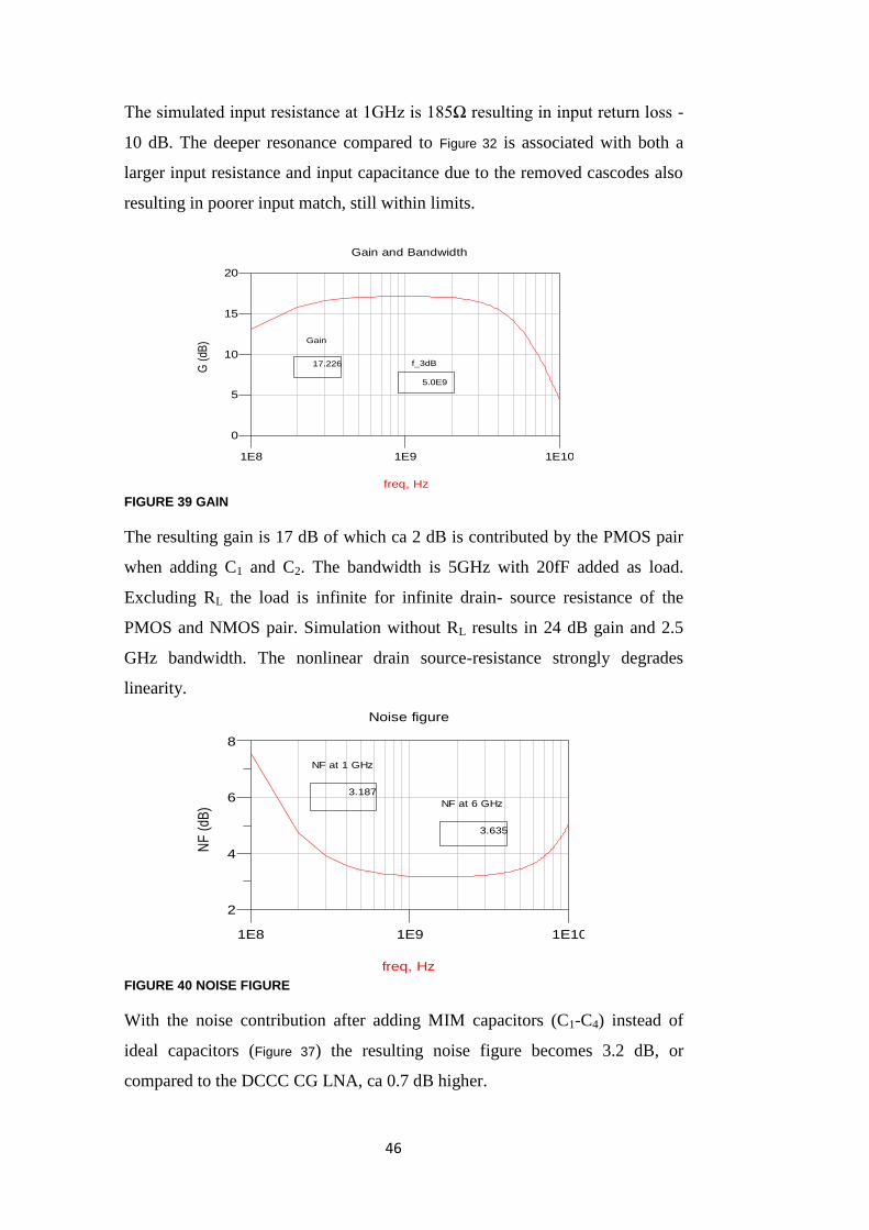
FIGURE 39 GAIN
The resulting gain is 17 dB of which ca 2 dB is contributed by the PMOS pair
when adding C1 and C2. The bandwidth is 5GHz with 20fF added as load.
Excluding RL the load is infinite for infinite drain- source resistance of the
PMOS and NMOS pair. Simulation without RL results in 24 dB gain and 2.5
GHz bandwidth. The nonlinear drain source-resistance strongly degrades
linearity.
FIGURE 40 NOISE FIGURE
With the noise contribution after adding MIM capacitors (C1-C4) instead of
ideal capacitors (Figure 37) the resulting noise figure becomes 3.2 dB, or
compared to the DCCC CG LNA, ca 0.7 dB higher.
1E91E8 1E10
5
10
15
0
20
freq, Hz
G (
dB)
Gain and Bandwidth
Gain
17.226 f_3dB
5.0E9
1E91E8 1E10
4
6
2
8
freq, Hz
NF
(dB
)
Noise figure
NF at 1 GHz
3.187
NF at 6 GHz
3.635
47
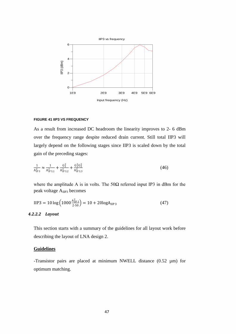
FIGURE 41 IIP3 VS FREQUENCY
As a result from increased DC headroom the linearity improves to 2- 6 dBm
over the frequency range despite reduced drain current. Still total IIP3 will
largely depend on the following stages since IIP3 is scaled down by the total
gain of the preceding stages:
1
A IP 32 ≈
1
A IP 3,12 +
G12
A IP 3,22 +
G12G2
2
A IP 3,32 (46)
where the amplitude A is in volts. The 50Ω referred input IP3 in dBm for the
peak voltage AIIP3 becomes
IIP3 = 10 log 1000A IIP 3
2
2∙50 = 10 + 20logAIIP 3 (47)
4.2.2.2 Layout
This section starts with a summary of the guidelines for all layout work before
describing the layout of LNA design 2.
Guidelines
-Transistor pairs are placed at minimum NWELL distance (0.52 µm) for
optimum matching.
2E9 3E9 4E9 5E91E9 6E9
2
4
0
6
Input frequency (Hz)
IIP3
(dB
m)
IIP3 vs frequency

48
-Signal routing is done by careful choice of metal widths and number of vias to
avoid parasitic resistances degrading performance, see Table 10 and Table 11.
- Parallel routing of input and output signals paths is avoided to minimize risk
of instability.
- The differential signal paths are wired symmetrically to minimize mismatch
and the length is minimized by careful floor planning and placement of the AC
coupling capacitors connecting each stage.
-Capacitors are placed at minimum distances to make the total area
consumption of the front-end as small as possible. Only small gaps are opened
where unavoidable, to connect capacitors to below metal layers.
-NWELL resistors are used for improved RF isolation. NWELLs (of all
components) are connected to the supply rail by wide metal wires (M1).
-Devices are pulled apart and large numbers of substrate contacts are placed
and connected to the ground rails to avoid latch up and to minimize substrate
noise [24].
Resistances (type values)
TABLE 10 METAL LAYERS
Metal Sheet resistance (mΩ/sq) Resistance (Ω), L=10 µm
1 (W=0.12 µm) 115 10
2,3,4,5,6 (W=0.14 µm) 105 7.5
7,8 (W=0.28 µm) 44 1.6
9 (W=0.56 µm) 27 0.45

49
TABLE 11 METAL VIAS
Mvia Resistance (Ω/Mv)
Mv1,2,3,4,5 1.3
Mv6 0.4
Mv7 1.1
Mv8 0.14
Mv1 to Mv8 8.24
4 x( Mv1 to Mv8) 2.06
8 x( Mv1 to Mv8) 1.03
Capacitance
The simulated parasitic capacitance for a metal 1 area of 270x170 µm is 317 fF
or 7 aF/µm2. Thus for signal routing this parasite can usually be neglected.
Current handling
According to the electro migration rules of the used CMOS process, the
maximum current density of the thinnest metal (M1) is 1.76 mA/µm. To keep
a good margin to where electro migration occurs, with a factor 2.5, the current
density of all metals should be kept below 0.7 mA/µm. The minimum metal
width is given by
Wmin= Idc/0.7 (48)
where Idc is in mA and Wmin in µm.
Example choosing number of transistor fingers: The quiescent current of the
differential LNA is 0.6 mA for each side. Thus the minimum metal width
should be 0.9 µm for all wiring carrying the dc current. The number of
transistor fingers is given as
2*0.9/0.16 - 1=11.25

50
where the metal width on each drain and source is 0.16 µm. To avoid current
crowding the width also need to be considered on the horizontal wire
connecting each finger to the 0.9 µm wire as shown in below figure.
FIGURE 42 STANDARD CELL RF NMOS TRIPPLE WELL
The number of fingers is here 12 and the width is 2.67 µm so the total width of the
NMOS input pair is 32 µm. Important, especially for the LNA is to choose the
number of fingers so that the gate resistance doesn’t increase the noise figure.
FIGURE 43 NOISE FIGURE VS TRANSISTROR FINGERS
Number of fingers is swept for the input pair at constant gate width 32 µm
(W=wf*nf). To avoid noise figure degradation due to the resistance of to long
gates, the number of fingers should be above 5.
5 10 15 20 25 300 35
2.8
3.0
3.2
3.4
2.6
3.6
Transistor fingers
NF
(dB
)
51
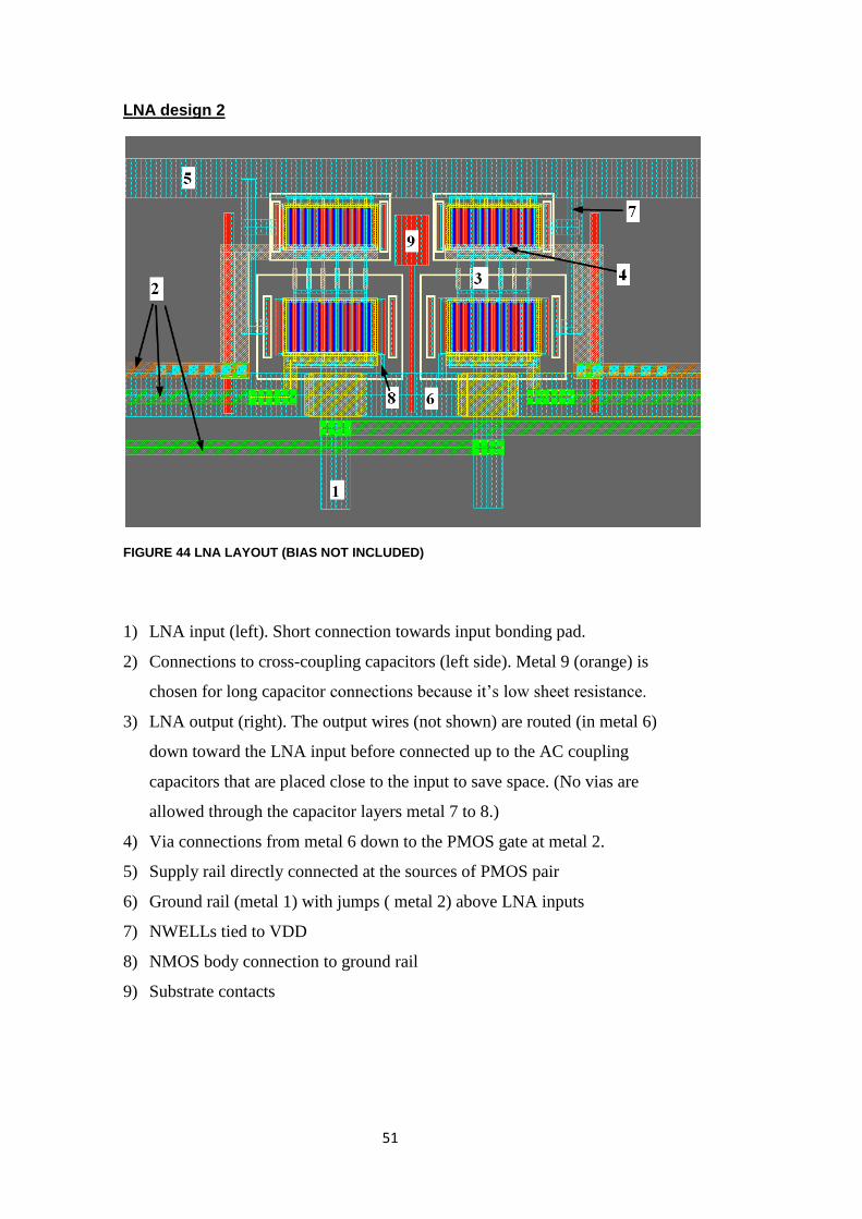
LNA design 2
FIGURE 44 LNA LAYOUT (BIAS NOT INCLUDED)
1) LNA input (left). Short connection towards input bonding pad.
2) Connections to cross-coupling capacitors (left side). Metal 9 (orange) is
chosen for long capacitor connections because it’s low sheet resistance.
3) LNA output (right). The output wires (not shown) are routed (in metal 6)
down toward the LNA input before connected up to the AC coupling
capacitors that are placed close to the input to save space. (No vias are
allowed through the capacitor layers metal 7 to 8.)
4) Via connections from metal 6 down to the PMOS gate at metal 2.
5) Supply rail directly connected at the sources of PMOS pair
6) Ground rail (metal 1) with jumps ( metal 2) above LNA inputs
7) NWELLs tied to VDD
8) NMOS body connection to ground rail
9) Substrate contacts

52
5 Down-conversion Mixer
5.1 Introduction
The frequency mixer needs to have good noise performance so that its input
referred noise does not overwhelm the amplified noise of the preceding LNA.
Since the mixer handles larger signals than the LNA its linearity must be
higher by at least a factor of the LNA gain to prevent the mixer from limiting
the receiver dynamic range.
5.1.1 Gilbert cell mixers
As a background to the passive mixer design in this work follows a brief
summary with properties of the Gilbert cell mixer.
M1 M2
Vb
vRF
Vb
vLO+ vLO-
RL
Vdd
M3
iout iout
RL
Vb
.
FIGURE 45 SINGLE BALANCED ACTIVE MIXER
Multiplication
In the Gilbert mixer above the incoming RF signal is converted to a current in
the transconductor stage (M3) so that multiplication is performed in the current
domain. The large amplitude of the LO signal turn on one transistor switch
(M1,M2) at the time so that the tail current is switched from one side to the
𝐼𝑑𝑐 + 𝑖𝑅𝐹 cos 𝜔𝑅𝐹𝑡
𝑖𝑜𝑢𝑡 (𝑡) = 𝑠𝑔𝑛 cos 𝜔𝐿𝑂𝑡 (𝐼𝑑𝑐 + 𝑖𝑅𝐹 cos 𝜔𝑅𝐹𝑡)
𝑖𝑀3 = 𝐼𝑑𝑐 + 𝑖𝑅𝐹 cos 𝜔𝑅𝐹𝑡

53
other at LO frequency. The output of this multiplication based mixer produce
the sum and difference frequencies of the two input signals. Compared to the
conventional two-port square-law mixer5, where multiplication result from
inherent nonlinearities, the Gilbert mixer is ideally linear and multiplication
arise from the implemented switching action. A general expression for
multiplication is given as
A cos ω1t ∙ B cos ω2 t = AB
2 cos( ω1 − ω2)t + cos( ωL + ω2)t (49)
The resulting output spectrum for a square wave LO signal multiplied with the
RF input is shown below.
ωLO 3ωLO 5ωLO 7ωLO
ωRFωLO - ωRF
3ωLO+ωRF
ω
PSD
FIGURE 46 SINGLE BALANCED MIXER OUTPUT SPECTRUM
Apart from the desired signal, the spectrum contains a large number of
unwanted components due to odd harmonics from the square wave LO signal.
The LO harmonics at the IF port here mainly result from mixing with the DC
component of the tail current but also from direct feed through due to limited
isolation between LO and IF ports. Finite port to port isolation strongly
depends on capacitive coupling between ports due to the transistor parasitic
capacitances. Therefore reducing transistor size is key to improve isolation.
Conversion gain
The conversion gain for the single balanced Gilbert mixer is given as
Gmix =iIF RL
vRF=
gm vRF RL
vRF∙
4
π∙
1
2=
2
πgm RL (50)
5 Typically a MOS transconductor with RF and LO in series at the gate and the IF port at the drain.
Suffer from poor isolation and mixing creates a host of unwanted signals including DC.
54
where the factor 4/π is the amplitude of the square wave fundamental
component and the factor ½ is because iIF is divided equally between the sum
and difference components [25].
Linearity
Linear V/I conversion is required to avoid distortion of a non constant envelope
RF signal in the transconductor as well as avoiding down-conversion of 3rd
order IM products created from nearby interferers. A commonly used
technique to linearize the transconductor is inductive source degeneration. Also
described in [25] is the MOS cross-quad using positive feedback and the MOS
cascomp with feedforward correction.
2nd
order distortion is also critical in the mixer mainly because it makes a Zero
IF receiver vulnerable to AM-detection of unwanted channels described in
section Even order distortion. Despite the balanced topology of the Gilbert mixer
several mechanisms are identified [26] as a source to 2nd
order distortion,
among the more known are .
Self-mixing
- The RF signal leak into the LO port. During the zero crossing of the LO
signal both transistors will be on so that the switching pair behave as an
analog multiplier5 squaring the RF signal. .
Transconductor nonlinearities
-In the double-balanced mixer mainly threshold voltage (vt) but also β6
mismatch in the transconductor pair degrades IP2.
Switching pair leakage
-The low frequency IM2 current at the output of the transconductor leak to
the IF port due to mismatch (vt ,β) in the switching pair.
Switching pair nonlinearities
-The fundamental limit to IIP2 is determined by the switching pair
nonlinearities [10]. .
6Technology dependent β =
𝜇𝑛 𝐶𝑜𝑥
2
𝑊
𝐿
55
SSB and DSB noise figure
The relation between the single sideband (SSB) and double sideband noise
figure (DSB) is NFSSB = NFDSB + 3 dB. A double sideband signal has
information at both RF and image frequency and therefore double signal power
at IF. Noise power on the other hand is equal at in and output both for SSB and
DSB signals (without filtering at the image frequency).
Thermal noise
Thermal noise is contributed by the transconductor and the switches as well as
the load resistors. The switches contribute noise to the output only when both
are on. When one is off it does not generate noise and the other that is on act as
a cascode transistor with its current fixed by the transconductor.
Transconductor thermal noise is down-converted to IF by the LO frequency
and it´s odd harmonics. The total white noise at the mixer output because of the
load, the transconductor and the switches is given as
vno2 = 8kTRL (1 + γ
2RL I
πA+ γgm RL ) (51)
The equation show how the output noise is effected by the LO amplitude A and
mixer DC bias current I and the load resistance RL [27].
Flicker noise
The main contributors of flicker noise in the Gilbert mixer are the switches.
Polysilicon resistors (unlike most resistors) are free of flicker noise and the
transconductor flicker noise is up-converted to LO frequency and to its odd
harmonics. Still small amounts of the transconductor flicker noise may appear
at the output due to mismatches in the transistor switches. The mechanisms for
the main contributions of flicker noise from the switches are
Direct switch noise
- The input referred flicker noise act as a slowly varying offset voltage
modulating the time for the zero-crossing thus changing the width of the
square wave output pulses. The pulse width modulation (PWM) of the
output waveform means that the flicker noise at the gates will appear at

56
the output without frequency translation. This effect may be minimized by
increasing the LO swing so that a steeper slope result in reduced
PWM. Increasing gate width of the transistors also reduce the effect of
direct switch noise. The input referred flicker noise is given by
vn2 =
1
f∙
K
WL Cox2 (V2/Hz) (52)
where K is a device specific constant.
Indirect switch noise
- In the indirect mechanism the flicker noise contribution to the output
depend on the parasitic capacitance Cp Figure 47. During switching Cp is
charged with a current proportional to the flicker noise voltage given as
in = 2fLO CPvn (53)
In contradiction to the direct mechanism this effect is not reduced by the
gate width since Cp include the parasitic capacitances of both switching
transistors. Instead for applications requiring a low flicker noise mixer a
method to reduce both direct and indirect noise is recently demonstrated
[28]. The switching current is reduced by current bleeding and inductors
are added that tune out Cp as shown for the double-balanced Gilbert mixer
below.

57
M1 M2 M4M3
LO-
LO+
RL RL
RF+ M5 RF-M6
LO+
M7 IbleedVb
IDC
FIGURE 47 LOW FLICKER NOISE DOUBLE BALANCED ACTIVE MIXER
The double-balanced mixer has the advantage of eliminating the LO
component in the IF output spectrum bye cancelation. With the two mixers
connected in anti parallel for the LO but parallel for the RF, the LO sum to
zero at the output. The high LO to IF isolation results in relaxed output
filtering. This comes at the expanse of double power consumption and a 3 dB
higher noise figure while gain is unchanged. .
5.1.2 Passive mixer
In the passive mixer flicker noise is eliminated since there is no bias current
involved. Instead the RF signal is switched directly in the voltage domain. That
is, for a voltage commuting passive mixer the transconductor is removed and
the RF input signal is switched directly into the high input impedance of the
first IF stage. Linearity is improved by avoiding V/I conversion of the RF input
signal. The passive mixer may also be implemented as a current commuting
mixer, driven by a current source and loaded with a low input resistance CG
stage instead of the CS stage as below.

58
M1 M2
VDD
CAC
DC
Vb
M4M3
CAC
IF AMP
RFin
LO-
LO+
Rb1
Rb3
IF+ IF-
Rb4
Vb
Rb2
FIGURE 48 DOUBLE BALANCED PASSIVE MIXER
Switch conductance .
With the switches connecting one input to one output at any given time, both
the nodes connecting each input pair to CAC will be kept charged to Vb. The
resulting gate-source bias voltage is here Vgs = VDD - Vb while the drain-source
voltage becomes zero. With the transistors biased in the linear region (Vb <
VDD), the switch conductance can be expressed as
gon = μnCoxW
L(vLO +vod ) (54)
goff = 0 (55)
where vod = vgs - vt and vLO is the peak voltage of a square wave LO signal.
Substituting the RF input signal into gon as (vLO-vRF+vod) show the RF
modulation of the switch conductance that may result in degraded linearity if
the input signal is allowed to increase.
Conversion gain .
In the ideal case for a square wave LO signal with the unit amplitude 4/π, the
conversion gain of the double-balanced passive mixer is given similarly as
above by

59
𝐆𝐦𝐢𝐱 =𝟒
𝛑∙
𝟏
𝟐=
𝟐
𝛑 (56)
Expressed in dB the gain is -4dB and for a sine wave LO signal with the unit
amplitude π/2 the gain becomes -2dB.
Noise
White noise is generated only due to the channel resistance of the switches that
are on at a given time, quantitatively resulting in a noise figure several dB
lower than the active counterpart. While the passive mixer is free of flicker
noise, the contributions from the LO output as well as the preceding LNA
result in direct switch noise and up-converted noise similarly as described for
the active mixer. .
5.2 Mixer design and simulation
Low flicker noise together with minimized 2nd
order distortion is main
priorities in the mixer design for a Zero IF receiver and therefore favorers the
use of a passive mixer for down-conversion to baseband [29]. The passive
mixer in Figure 48 is simply realized with four transistors biased in the linear
region. LO ports are driven by a sine wave LO signal with 1 V differential peak
to peak voltage and with the gates biased at the threshold to achieve a
maximally hard switching characteristic. As a low on-resistance in the analog
transistor switches improves linearity due to the large voltage division ratio
between Rb and the nonlinear on-resistance, it also results in low RF port input
resistance. The transistor in the simulated mixer below are small size with the
gate width 6µm and on resistance of ca 1100Ω (Figure 49) to favor a high input
resistance as to relax the loading conditions for the mixer driver [30]. While
this approach degrades linearity as well as noise figure due to increase channel
noise, it benefits from improved total gain and bandwidth as well as reduced
power consumption in the driver. Combined with an efficient linearization
method demonstrated in [31] using complementary PMOS switches to reduce
the RF modulation of the conductance, this design approach still allows for
high overall performance.
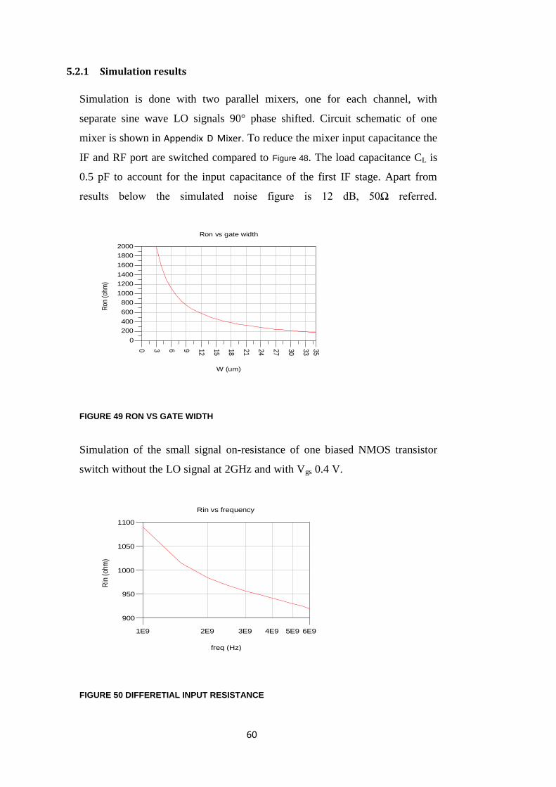
60
5.2.1 Simulation results
Simulation is done with two parallel mixers, one for each channel, with
separate sine wave LO signals 90° phase shifted. Circuit schematic of one
mixer is shown in Appendix D Mixer. To reduce the mixer input capacitance the
IF and RF port are switched compared to Figure 48. The load capacitance CL is
0.5 pF to account for the input capacitance of the first IF stage. Apart from
results below the simulated noise figure is 12 dB, 50Ω referred.
FIGURE 49 RON VS GATE WIDTH
Simulation of the small signal on-resistance of one biased NMOS transistor
switch without the LO signal at 2GHz and with Vgs 0.4 V. .
FIGURE 50 DIFFERETIAL INPUT RESISTANCE
3 6 9 12 15 18 21 24 27 30 330 35
200
400
600
800
1000
1200
1400
1600
1800
0
2000
W (um)
Ron
(oh
m)
Ron vs gate width
2E9 3E9 4E9 5E91E9 6E9
950
1000
1050
900
1100
freq (Hz)
Rin
(oh
m)
Rin vs frequency

61
The RF port input resistance shows frequency dependence due to the parasitic
capacitances of the switches. The simulated input capacitance is 48fF to 16fF
over the frequency range. These results are used in the buffer design.
FIGURE 51 CONVERSION GAIN VS FREQUENCY
With a 50 kΩ differential load implemented with HR (high resistance)
resistors, to limit the required area of such a large resistance, the resulting
conversion gain is almost constant at -1.7 dB over the frequency range.
Two tone test:
Input tone 1: 20mV, 1GHz
Input tone 2: 20mV, 1GHz + 1MHz
LO frequency 1 GHz + 5MHz
2E9 3E9 4E9 5E91E9 6E9
-1.80
-1.75
-1.70
-1.65
-1.85
-1.60
frequency (Hz)
G (
dB)
Conversion Gain
2.5 3.0 3.5 4.0 4.5 5.0 5.5 6.0 6.52.0 7.0
-150
-100
-50
-200
0
freq (MHz)
Vou
t (dB
v)
Readout
Aout
Readout
AIM3
IF Output Spectrum
Aout
freq=
dB(HB.Vload)=-35.746
5.000MHz
AIM3
freq=
dB(HB.Vload)=-114.180
6.000MHz

62
Aout = −37.7 dBv → 16 mV
AIM 3 = −114.2 dBv → 2.1 μV (57)
AIIP 3 = Ain Aout
A IM 3= 1.7 V (58)
Referring to 50Ω:
IIP3 = 10 log 1000A IIP 3
2
2∙50 = 10 + 20logAIIP 3 = 14.6 dBm (59)
Swept two tone test:
FIGURE 52 IIP3 VS FREQUENY
FIGURE 53 FLICKER NOISE
The passive mixer shows an extremely low flicker corner below 10 kHz.
Sweeping the output noise voltage vs. gate length shows no change of flicker
corner while thermal noise (ca 3nV above) changes as expected with respect to
channel resistance. .
2.0E9 3.0E9 4.0E9 5.0E91.0E9 6.0E9
15.0
15.5
16.0
16.5
17.0
14.5
17.5
frequency (Hz)
IIP3
(dB
m)
IIP3 vs frequency
10.00k 100.0k1.000k 1.000M
4.000n
5.000n
3.000n
6.000n
freq (Hz)
Vout
_noi
se (V
)
Flicker noise corner

63
As a comparison the simulation results for a mixer with 30 µm gate length
show a noise figure at 7.6 dB while input impedance is reduced to 480Ω-220Ω
and 260fF-100fF over the frequency range.
5.2.2 Layout
Introduction in section Layout 4.2.2.2
Floorplan
M1 M3
M2 M4
Drain
Source
Drain
Source
Source
Drain
Source
Drain
FIGURE 54 MIXER FLOORPLAN
Compare to Figure 48 double balanced passive mixer.
Passive mixer Layout
FIGURE 55 PASSIVE MIXER LAYOUT (BIAS NOT INCLUDED)

64
The transistor placement allow for symmetrical routing of both IF and RF
ports. Also mismatch7 from asymmetrical routing of the LO signal to the gates
is avoided by placing the vias at metal 2 (yellow) equally spaced between the
gates. (Note that IF and RF ports are switched as commented in above
simulation.)
6 Intermediate stages
Due to the large gain-bandwidth product requirement of the RF front-end,
the output pole of the LNA created by its load resistance and output
capacitance will unavoidably result in limited bandwidth. In addition to this,
the passive mixer is preferably driven by a source-follower with its input
capacitance loading the LNA. To extend the bandwidth a shunt peaked
intermediate gain stage (GS) is used. Before arriving at the gain stage Figure 56,
several versions of the architecture where tested including
- CCC CG stage with the input resistance 1/gm as LNA load
- Active PMOS loads directly driving the mixer
- Shunt peaking with active inductor loads including current bleeding
7 This is not as critical for a mixer with relative high impedance inputs compared to a mixer with
50 ohm inputs.
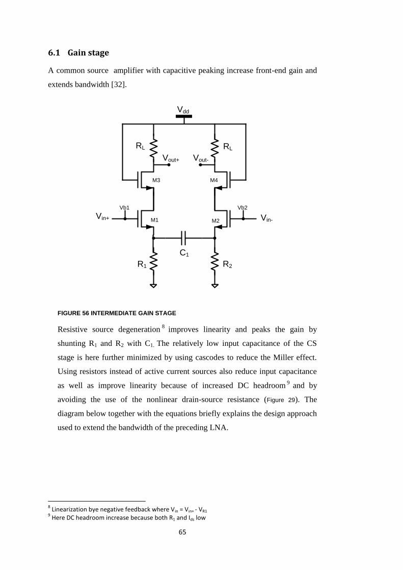
65
6.1 Gain stage
A common source amplifier with capacitive peaking increase front-end gain and
extends bandwidth [32].
Vdd
M1 M2
M3 M4
Vb1 Vb2
Vout-Vout+
RL RL
R1 R2
C1
Vin-Vin+
FIGURE 56 INTERMEDIATE GAIN STAGE
Resistive source degeneration8
improves linearity and peaks the gain by
shunting R1 and R2 with C1. The relatively low input capacitance of the CS
stage is here further minimized by using cascodes to reduce the Miller effect.
Using resistors instead of active current sources also reduce input capacitance
as well as improve linearity because of increased DC headroom9 and by
avoiding the use of the nonlinear drain-source resistance (Figure 29). The
diagram below together with the equations briefly explains the design approach
used to extend the bandwidth of the preceding LNA.
8 Linearization bye negative feedback where Vin = Vin+ - VR1
9 Here DC headroom increase because both R1 and Ids low
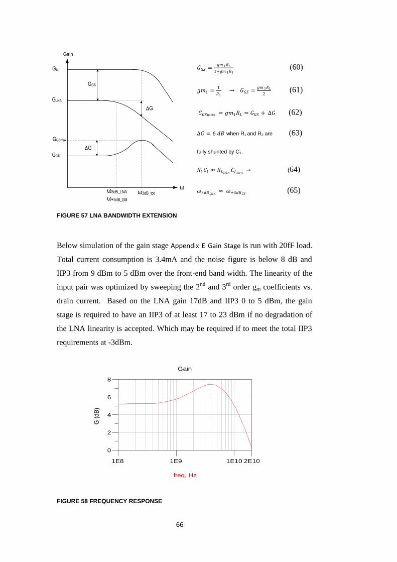
66
ω
Gain
GLNA
GGSmax
GGS
Gtot
∆G
∆G
GGS
ω3dB_LNA
ω+3dB_GS
ω3dB_tot
FIGURE 57 LNA BANDWIDTH EXTENSION
Below simulation of the gain stage Appendix E Gain Stage is run with 20fF load.
Total current consumption is 3.4mA and the noise figure is below 8 dB and
IIP3 from 9 dBm to 5 dBm over the front-end band width. The linearity of the
input pair was optimized by sweeping the 2nd
and 3rd
order gm coefficients vs.
drain current. Based on the LNA gain 17dB and IIP3 0 to 5 dBm, the gain
stage is required to have an IIP3 of at least 17 to 23 dBm if no degradation of
the LNA linearity is accepted. Which may be required if to meet the total IIP3
requirements at -3dBm.
FIGURE 58 FREQUENCY RESPONSE
𝐺𝐺𝑆 =𝑔𝑚 1𝑅𝐿
1+𝑔𝑚 1𝑅1 (60)
𝑔𝑚1 =1
𝑅1 → 𝐺𝐺𝑆 =
𝑔𝑚 1𝑅𝐿
2 (61)
𝐺𝐺𝑆𝑚𝑎𝑥 = 𝑔𝑚1𝑅𝐿 = 𝐺𝐺𝑆 + ∆𝐺 (62)
∆𝐺 = 6 𝑑𝐵 when R1 and R2 are (63)
fully shunted by C1.
𝑅1𝐶1 ≈ 𝑅𝐿𝐿𝑁𝐴𝐶𝐿𝐿𝑁𝐴
→ (64)
𝜔3𝑑𝐵𝐿𝑁𝐴≈ 𝜔+3𝑑𝐵𝐺𝑆
(65)
1E9 1E101E8 2E10
2
4
6
0
8
freq, Hz
G (
dB
)
Gain

67
6.1.1 Layout
Introduction See section Layout 4.2.2.2
Gain stage layout
FIGURE 59 GAIN STAGE LAYOUT (DETAIL)
1) Input (left side). Via connections from AC coupling capacitor down to
metal 2 on the gate of transistor M1 (Figure 56 ). 18 vias from metal 8
down to metal 2 are placed along the gate so that its total resistance is
below 0.5Ω.
2) Via connections to shunt capacitor C1
3) Output (right side).
4) R2 (50Ω) implemented with two parallel N-poly resistors (low sheet
resistance) of 100Ω each, connected directly down to the ground rail (not
shown). The resistor width 10 µm is relatively large to avoid smaller
resistor geometry from degrading accuracy. Discrepancies from the
resistance values of R2 and RL will result in incorrect gain and signal path
mismatch.
5) Load resistor RL implemented with two series N-poly resistors, 140Ω each.
6) NWELL connection to supply rail

68
6.2 Buffer
A balanced source follower stage, modified with the input signal cross coupled
to the current sources is chosen to drive the I/Q mixer.
Vdd
M4
M2
Vb2
Rb
Vin-
M3
M1
Vb1 Vin+
Cc Cc
Rb
Vout+ Vout-
FIGURE 60 BUFFER STAGE
The gain of this stage is improved by cross-coupling the current sources as a
common source pair (M3, M4) working in parallel with the source follower
across the load. The low output resistance10
2/gm1 allow for high bandwidth
and minimal loss driving a low load resistance. AC-coupling capacitors split
the signal into I and Q paths as shown in below figure. .
I/Q Mixer
1/gm1
1/gm2
Buffer
I channel
Q channel
Rinmix1
Rinmix2
RFin
FIGURE 61 BUFFER STAGE AND I/Q MIXER
10
Same as the input resistance of the differential common gate stage 2/gm1 = 1/gm1 +1/gm2

69
Gain
The buffer gain can be expressed as
GB ≈ 1 +gm 3
gm 1 (66)
This approximation show the gain is independent of the load which avoids the
nonlinear mixer input resistance from limiting the bandwidth as when driving
the mixer directly with the gain stage.
Input capacitance
The Miller effect in the common source stage increases the input capacitance,
here expressed as
Cin =1
2(Cgs + Cgd GB) (67)
where the parasitic capacitances for the MOS transistor in saturation is given
bye
Cgs ≈2
3Cox WL ;gate-source capacitance (68)
Cgd = Cov ;gate-drain capacitance (69)
Cov ≈ Cox WLD =Cox WL
5 ;overlap capacitance assuming the overlap LD
is a fifth of the channel length L (70)
→ Cgs =10
3Cgd → Cin = Cgd (
5
3+
GB
2 ) (71)
For the buffer stage with gain 3 dB and M3,M4 with the gate width 40µm and
minimum channel length transistors of the UMC 90nm process with Cox
0.0117 F/m2 , the calculated input capacitance is 20 fF. This result indicates
how the design of the buffer will limit the bandwidth of the preceding gain
stage by contributing with Cin to its output pole. Below simulation results are
based on the buffer schematic in Appendix F Buffer. The load is 900Ω and 20fF
based on simulated mixer input impedance Figure 50.

70
FIGURE 62 GAIN
While ca 6 dB is won in gain, compared to a simulation of the usual balanced
source follower, the simulated IIP3 is ca 10 dBm over the frequency range
which is more than 11 dBm lower11
.
6.2.1 Layout
Introduction See Layout 4.2.2.2
Buffer layout
FIGURE 63 BUFFER LAYOUT(OVERVIEW)
11
The SF was biased at the double current which makes the IIP3 comparison a bit
overestimated.
1E9 1E101E8 2E10
-2
0
2
-4
4
freq, Hz
G (
dB)
Gain and Bandwidth
Gain
2.713 f_3dB
12.2E9
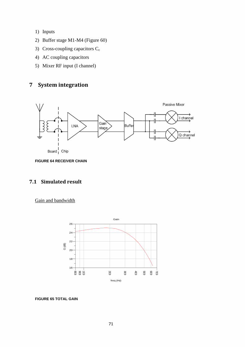
71
1) Inputs
2) Buffer stage M1-M4 (Figure 60)
3) Cross-coupling capacitors Cc
4) AC coupling capacitors
5) Mixer RF input (I channel)
7 System integration
FIGURE 64 RECEIVER CHAIN
7.1 Simulated result
Gain and bandwidth
FIGURE 65 TOTAL GAIN
9E
8
1E
9
2E
9
3E
9
4E
9
5E
9
6E
9
8E
8
7E
9
18
20
22
24
16
26
freq (Hz)
G (
dB
)
Gain

72
The total gain of the receive chain from LNA input to one mixer output at IF
5MHz was determined with a swept HB simulation shown in Appendix F Test
bench, including the LNA, GS, Buffer and Mixer blocks as designed in there
respective appendices C, E, F and D. After optimizing the overshoot with the
shunt capacitor in the gain stage, the maximum gain and bandwidth is ca 25 dB
and 4 GHz. .
Noise figure
FIGURE 66 NOISE FIGURE EXCEPT MIXER
The noise figure above is determined with s-parameter simulation without the
mixer. The total noise figure was calculated after referring the output noise,
3nV of each mixer, to the LNA input as described in section 4.1.2 resulting in
the total noise figure of 6 dB at 1 GHz. With the mixer having a constant gain,
an estimated total noise figure vs. frequency is given by adding 2.4 dB to the
result in Figure 66.
Power consumption
The power consumption including bias nets is ca 7.1mW with the contributions
1.7mW, 4mW and 1.4mW from LNA, GS and Buffer respectively.
Linearity
A two tone test determined total IIP3 to -20 dBm at 3.5 GHz. Below diagram
1E91E8 1E10
4
6
8
2
10
freq (Hz)
NF
(dB
)
Noise figure
NF at 1 GHz
3.611
NF at 6 GHz
4.410

73
show the distribution of the receiver performance including the above total
gain, noise figure and IIP3.
FIGURE 67 CASCADED PERFORMANCE
A HB simulation at 1GHz determines gain at the output of each block with all
blocks in cascade. The noise figure distribution reveals the large increment due
to the mixer noise. A 10 dBm reduction of IIP3 is seen after the second stage.
Also noted was that IIP3 of the LNA was reduced from ca 5 dBm at 3.5GHz
(Figure 41) to 0.4 dBm, despite the high input impedance of the following gain
stage.
TABLE 12 RECEIVER CHAIN PERFORMANCE
Switch/
Duplexer LNA-GS-Buffer-Mixer VGA
Cascaded
performance
Receiver
specification
Gain (db) -2 24,6 14 36,6 35
NF (dB) 2 6 7 8 8
IIP3 (dBm) ∞ -20 15 -18,4 -3
The table above show the receive chain performance based on the simulated
results in Figure 67 and the block specifications presented in section 3.3.4. The
cascaded NF and IIP3 are calculated based on Friis equation (5) and cascaded
IIP3 equation (46). The result show, compared to Figure 67, that adding the VGA
does not affect the total noise figure or IIP3. The improved IIP3 result from the
attenuation in the duplexer added in front of the LNA.
17,123
25,924,6
3,2 3,6 3,6 6
0,4
-9,7-14,2 -20
Cascaded performance
Gain (dB) NF (dB) IIP3 (dBm)
LNA GS Buffer Mixer

74
7.2 Layout
FIGURE 68 RECEVER FRONT-END LAYOUT (BIAS NOT INCLUDED)
Individual blocks are described in respective layout section. Also shown here
are the LNA cross-coupling capacitors and the long bias resistors, below the I
and Q mixers, connected to mixer LO and IF ports.
Post layout simulation
After adding parasitic resistances in the schematic due to metal wires and vias
in the signal paths from the LNA input to the mixer output, and also changing

75
the number of transistor fingers as chosen for the layouts, the same simulation
was run that was done for noise figure and gain in Figure 65 and Figure 66.
The simulated result showed that noise figure was improved by 0.2 dB despite
the increased signal path resistance, because of the increased number of
fingers. The gain was reduced by ca 1 dB for the bandwidth 4 GHz.
8 Conclusion
A 90 nm CMOS wideband receiver front-end supporting pre-4G, WiMAX and
LTE standards have been designed. The design exemplifies some of the typical
requirements and design challenges that future fully integrated radio receivers
for 4G will be required to meet. A top down approach have been used where
inductor less circuit topologies suitable for integration was selected. Multi-
standard receiver budget analysis was performed for a Zero IF/Low
architecture and performance parameters where extracted for the design of
LNA and down-conversion mixers. The circuit design includes two versions of
the dual capacitive cross-coupling common gate LNA (DCCC CG LNA).
While LNA design 1 shows overall somewhat better performance, in particular
input matching, design 2 has the advantage of a compact size layout and higher
linearity. The double balanced passive mixer was designed for voltage
commuting operation and shows extremely low flicker noise. Regarding
achieved receiver performance; noise figure, gain and bandwidth are within
reach of specified requirements while linearity showed more challenging to
meet. Still very low power consumption as well as a compact size layout
allows for improved linearity by additional circuit level linearization
techniques.

76
9 Appendix A Dual CCC CG LNA
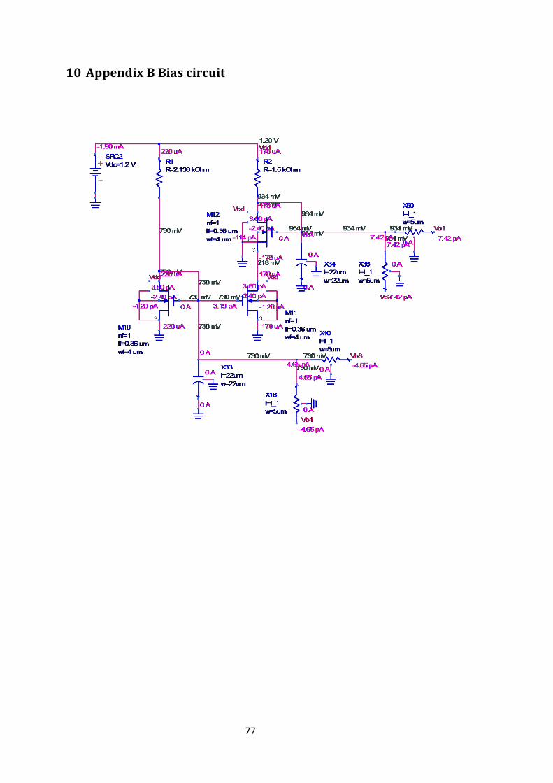
77
10 Appendix B Bias circuit

78
11 Appendix C OSI DCCC CG LNA

79
12 Appendix D Mixer

80
13 Appendix E Gain Stage

81
14 Appendix F Buffer

82
15 Appendix F Test bench

83
16 Bibliography
[1] J.L. Mehta, (Feb.2001.) “Transceiver architectures for wireless ICs,” www.
rfdesign.com [Online], Available: http://mobiledevdesign.com/images/
archive/0201Mehta76.pdf
[2] B. Razavi, “RF Microelectronics,” Upper Saddle River: Prentice Hall, 1998.
[3] J. Crols and M.S.J. Steyaert, ”Low-IF Topologies for High-Performance
Analog Front Ends of Fully Integrated Receivers,” IEEE Trans. Circuits and
systems II, Volume 45, pp. 269 - 282, March. 1998.
[4] K.W. Martin, “Complex Signal Processing is not Complex,” IEEE Trans.
Circuits and systems I, Volume 51, pp. 1823 – 1836, Sept. 2004
[5] H. Darabi et al., ”A 2.4-GHz CMOS Transceiver for Bluetooth,” IEEE Jour.
Solid state circuits, Volume 36, pp. 2016 – 2024, Dec. 2001
[6] T. Hornak, (Jun. 2002) “Using Polyphase filters as image attenuators,”
www.rfdesign.com [Online], Available: http://images.rfdesign.com/files/4/
0601Hornak26.pdf
[7] S. Lowe, “LTE vs. WiMAX,” IET Institution of Engineering and Technology,
pp. 1-38, Sept. 2007.
[8] “Long-Term Evolution (LTE): The vision beyond 3G,” Nortel, pp. 1-6, 2008.
[9] J. Sharony, “Introduction to Wireless MIMO – Theory and
Applications,” IEEE Long Island Section, pp. 1-63, Nov. 2006
[10] S. Rodriguez, “Wideband RF front-ends,” Unpublished work, Dept ECS
Royale Institute of Technology (KTH), Stockholm 2008.
[11] S. Chehrazi et al., “A 6.5GHz Wideband CMOS Low Noise Amplifier for
Multi-Band Use,” Proc. IEEE Custom Integrated Circuits Conference, pp.
801 – 804, Sept. 2005.
[12] “IEEE Standard for Local and metropolitan area networks Part 16: Air
Interface for Fixed and Mobile Broadband Wireless Access Systems
Amendment 2: Physical and Medium Access Control Layers for Combined
Fixed and Mobile Operation in Licensed Bands and Corrigendum 1,“ IEEE
Std 802.16e-2005 and IEEE Std 802.16-2004/Cor1-2005, pp. 1-864, Feb.
2006.
[13] “3GPP TS 36.101 V8.0.0; 3rd Generation Partnership Project; Technical
Specification Group Radio Access Network; Evolved Universal
Terrestrial Radio Access (E-UTRA); User Equipment (UE) radio
transmission and reception (Release 8),” Technical Specification,
84
3GPP, pp.1-45,Dec. 2007.
[14] S. Rodriguez, “Receiver budget study,” Unpublished work, Dept ECS
Royale Institute of Technology (KTH), Stockholm 2008.
[15] D. Enright et al., “Continuous-Time Sigma-Delta ADC in 1.2-V 90-nm
CMOS with 61-dB Peak SNDR and 74-dB Dynamic Range in 10-MHz
Bandwidth,” Fujitsu Scientific & Technical Journal, Volume 44, pp. 264-273,
July 2008.
[16] T. Chang et al., “A Packaged and ESD-Protected Inductorless 0.1-8 GHz
Wideband CMOS LNA,” IEEE Microwave and Wireless Components Letters,
Volume 18, pp. 416 – 418, June 2008.
[17] A. Ismail and A.A. Abidi, “A 3–10-GHz Low-Noise Amplifier With
Wideband LC- Ladder Matching Network,” IEEE Journal of Solid-State
Circuits, Volume 39, pp. 2269 – 2277, Dec. 2004.
[18] S.C. Blaakmeer et al., “An Inductorless Wideband Balun-LNA in 65nm
CMOS with balanced output,” ESSCIRC Solid State Circuits Conference, pp.
364 – 367, Sept. 2007.
[19] A. Amer et al., “A Low Power Wideband CMOS LNA for WiMAX,” IEEE
Trans. Circuits and systems II, Volume 54, pp. 4 – 8, Jan. 2007.
[20] A. Rofougaran et al., “A 1 GHz CMOS RF Front-End IC for a Direct-
Conversion Wireless Receiver,” IEEE Journal of Solid-State Circuits,
Volume 31, pp. 880 – 889, July 1996.
[21] W. Zhuo et al., “A Capacitor Cross-Coupled Common-Gate Low-Noise
Amplifier,” IEEE Trans. Circuits and Systems II, Volume 52, pp. 875 –
879, Dec.2005.
[22] D. A. Johns and K. Martin, “Analog Integrated Circuit Design,”
Crawfordsville: Wiley & Sons, Inc., 1996.
[23] P.-I. Mak et al., “An Open-Source-Input, Ultra-Wideband LNA with Mixed-
Voltage ESD Protection for Full-Band (170-to-1700 MHz) Mobile TV
Tuners,” IEEE International Symposium on Circuits and Systems, pp. 668 –
671, May 2008.
[24] C. Saint, “IC Mask Design,” New York: McGraw-Hill, 2002.
[25] T. H. Lee, “The Design of CMOS Radio-Frequency Integrated Circuits,”
Cambridge: Cambridge University Press, 2004.

85
[26] D. Manstretta et al., “Second-Order Intermodulation Mechanisms in CMOS
Downconverters,” IEEE Journal of Solid-State Circuits, Volume 38, pp. 394
– 406, March 2003.
[27] H. Darabi and A.A. Abidi, “Noise in RF-CMOS Mixers: A Simple Physical
Model,” IEEE Journal of Solid-State Circuits”, Volume 35, pp. 15 – 25, Jan.
2000.
[28] J. Park et al., “Design and Analysis of Low Flicker-Noise CMOS Mixers for
Direct-Conversion Receivers,“ IEEE Trans. Microwave Theory and
Techniques, Volume 54, pp. 4372 – 4380, Dec. 2006.
[29] R. Bagheri et al., “An 800-MHz - 6 GHz Software-Defined Wireless
Receiver in 90-nm CMOS,” IEEE Journal of Solid-State Circuits, Volume
41, pp. 2860 – 2876, Dec. 2006.
[30] M. Camus et al., “A 5.4mW 0.07mm2 2.4GHz Front-End Receiver in 90nm
CMOS for IEEE 802.15.4 WPAN,” IEEE International Solid State Circuits
Conference, pp. 368 – 620, Feb. 2008.
[31] S. Zhou et al., “A CMOS Passive Mixer With Low Flicker Noise for Low-
Power Direct-Conversion Receiver,” IEEE Journal of Solid-State Circuits,
Volume 40, pp. 1084 – 1093, May 2005.
[32] A. Leuciuc et al., “A Highly Linear Low-Voltage MOS Transconductor,”
IEEE International Symposium on Circuits and Systems, Volume 3, pp. 735 –
738, May 2002.