recipe: charge sharing! - eecs instructional support … · recipe: charge sharing! march 16, ......
TRANSCRIPT
Recipe: Charge Sharing!
March 16, 2017
1 What Is Charge Sharing?
Charge sharing, quite simply, is the sharing of charges among capacitors. Youhave entered this section of our esteemed cookbook having conquered the messybut rewarding world of resistive circuits. With blood afresh on your hands,and armed with the fruits of your toil, it is now time for you, the intrepid 16ACircuit Solver, to tackle that elusive final frontier: capacitors.
Before we charge headlong into battle, let’s recall a few ground rules aboutcapacitors1:
• In steady state, no current flows through them2
• In steady state, charges will be stored on the parallel plates of each ca-pacitor. The charges stored on each plate of a capacitor will be equal inmagnitude, and opposite in sign.
• These charges, stored on the parallel plates of a capacitor, go hand-in-hand with a voltage difference across the plates of the capacitor. Voltagealways drops from the plate holding positive charge to the plate holdingnegative charge.
A lot of capacitor problems involve circuits with essentially voltage/currentsources, capacitors, and switches. We can play around with opening and closingthese switches, basically creating different phases of the circuit. Each phaseactually corresponds to a different circuit. But these circuits are all linked toone another. Between two consecutive phases, the charges will move betweendifferent capacitors. This charge sharing recipe will help us formalize how, andwhere, charge is shared in the circuit, and give us a tried and tested method toapproach these problems. In other words, it is our battle armor, and needlessto say, shock-proof.3
Oh, also. We can hear you asking. Why might people want to make thesecircuits? You’ll find out soon.
1We’ll give you a second to collectively groan at those horrible, horrible puns2It simply can’t! Capacitors are, simplistically, just parallel plates with a non-conducting
material (more accurately, a dielectric) between them.3Again, profuse apologies.
1
2 Total Prep Time
Anywhere from five minutes to five hours depending on your circuit... Ok justkidding, we’re nice people.
3 Ingredients
• Your circuit (which usually has more than one “phase” depend-ing on the positions of the switches in the circuits)
• Sign conventions
• Circuit drawing skillz
• Identification of nodes in a circuit
• Relationship between charge and voltage across a capacitor
• Law of conservation of charge
• Branch voltages and KVL
4 Directions
1. Branch voltage labeling: Label the voltages across all the capacitors.Choose whichever direction (polarity) you want for each capacitor – thismeans you can mark any one of the plates with the + sign, and thenyou can mark the other plate with the − sign. Just make sure you stayconsistent with this polarity across phases!
2. Circuit drawing: Draw the circuit in each phase. Remember: keeppolarities of voltages consistent across all phases!
3. (Using your solution for the circuit in phase i−1) Solve the circuitin phase i!
(a) Identify all the nodes in the circuit. As in nodal analysis, an intersec-tion of two or more elements constitutes a node. Label all the nodevoltages.
(b) Write the voltage differences across each capacitor according to thepolarities you have defined and the node voltages you labeled earlier.
(c) Use the relationship between charge and voltage across a capacitor(Q = CV ) to determine the charge on each plate on each capacitor,in terms of the node voltages and capacitances. (Stop to taste: Makesure to convince yourself of the sign of charge on each plate! Theplate marked with the + sign should have charge +Q, and the platemarked with the − sign should have charge −Q.)
2

(d) Identify the floating nodes. Floating nodes are nodes that are notconnected to a voltage source or an explicit ground.4 For each floatingnode, mark the plates of capacitors that are connected to it. Then,the law of conservation of charge for this floating node says: “Thetotal charge on these plates will remain the same in phase i andphase i − 1!” Why do you think this is true? Because these chargesare basically shared between the plates – they can travel from oneplate to another, but they cannot go anywhere else.
(e) Write the equation for charge conservation at all the floating nodesin phase i. At this point, you may need to write KVL to find thevoltage that you are trying to solve for. Hence, determine the nodevoltages in the circuit for phase i.
(f) Using the node voltages, determine the voltage difference across allthe capacitors according to the polarities marked. Then, calculatethe charge stored in each capacitor. We have now solved the circuitfor phase i! Hooray.
4. Repeat step 3 until all phases are done.
5. Your circuit is now solved and demystified! It’s now time toenjoy the fruits of your toil, which are...more circuits. We’resorry.
5 Example Circuit 1 - Capacitance Sensor
Let’s begin with the following circuit. You may be familiar with it fromthe capacitive touch-screen lab:
+
–
φ1 φ2
Vin
C1 C2
φ1
The switches labeled φ1 are closed in phase 1 and open in phase 2. Theswitches labeled φ2 are open in phase 1 and closed in phase 2. When a
4Keep in mind that nodes that we set as reference nodes are still floating nodes, unlessthey were explicitly set to ground. If this is confusing, don’t worry about it too much.
3
switch is ”open” it behaves like an open circuit. When a switch is ”closed”it behaves like a short circuit.
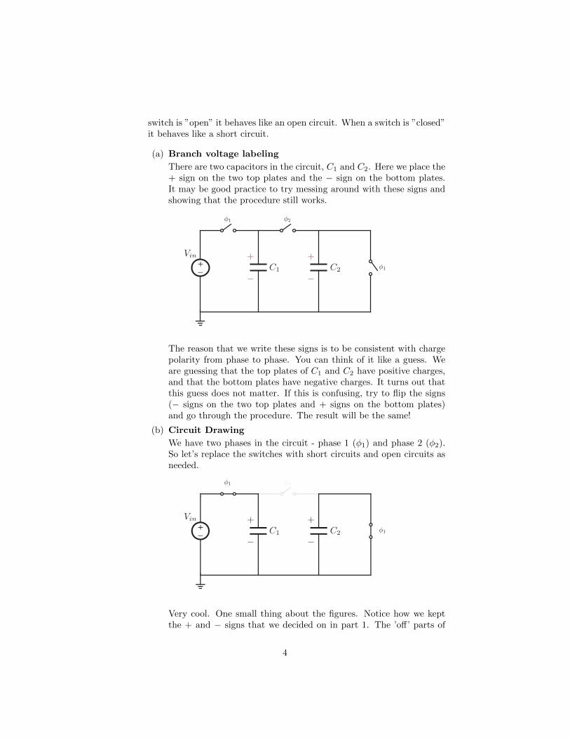
(a) Branch voltage labeling
There are two capacitors in the circuit, C1 and C2. Here we place the+ sign on the two top plates and the − sign on the bottom plates.It may be good practice to try messing around with these signs andshowing that the procedure still works.
+
–
φ1 φ2
Vin
C1 C2 φ1
+
−
+
−
The reason that we write these signs is to be consistent with chargepolarity from phase to phase. You can think of it like a guess. Weare guessing that the top plates of C1 and C2 have positive charges,and that the bottom plates have negative charges. It turns out thatthis guess does not matter. If this is confusing, try to flip the signs(− signs on the two top plates and + signs on the bottom plates)and go through the procedure. The result will be the same!
(b) Circuit Drawing
We have two phases in the circuit - phase 1 (φ1) and phase 2 (φ2).So let’s replace the switches with short circuits and open circuits asneeded.
+
–
φ1 φ2
Vin
C1 C2 φ1
+
−
+
−
Very cool. One small thing about the figures. Notice how we keptthe + and − signs that we decided on in part 1. The ’off’ parts of
4
+
–
φ1 φ2
VinVV
C1 C2 φ1
+
−
+
−
the circuit are greyed out so that you can see exactly how we modifythe circuit between the two phases.
(c) Solve the circuit!
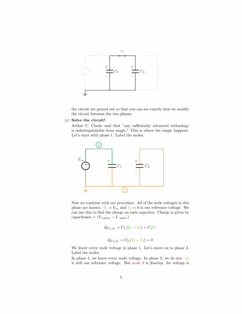
Arthur C. Clarke said that ”any sufficiently advanced technologyis indistinguishable from magic.” This is where the magic happens.Let’s start with phase 1. Label the nodes.
+
–
Vin
C1 C2
+
−
+
−
1
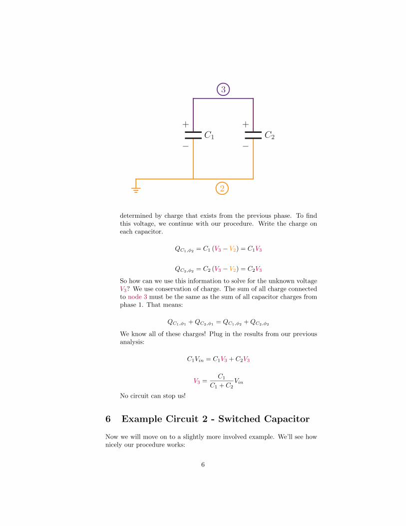
2
Now we continue with our procedure. All of the node voltages in thisphase are known. V1 = Vin and V2 = 0 is our reference voltage. Wecan use this to find the charge on each capacitor. Charge is given bycapacitance × (V+plate − V−plate)
QC1,φ1= C1 (V1 − V2) = C1V1
QC2,φ1= C2 (V2 − V2) = 0
We know every node voltage in phase 1. Let’s move on to phase 2.Label the nodes.
In phase 1, we knew every node voltage. In phase 2, we do not. V2is still our reference voltage. But node 3 is floating. Its voltage is
5
C1 C2
+
−
+
−
3
2
determined by charge that exists from the previous phase. To findthis voltage, we continue with our procedure. Write the charge oneach capacitor.
QC1,φ2= C1 (V3 − V2) = C1V3
QC2,φ2 = C2 (V3 − V2) = C2V3
So how can we use this information to solve for the unknown voltageV3? We use conservation of charge. The sum of all charge connectedto node 3 must be the same as the sum of all capacitor charges fromphase 1. That means:
QC1,φ1+QC2,φ1
= QC1,φ2+QC2,φ2
We know all of these charges! Plug in the results from our previousanalysis:
C1Vin = C1V3 + C2V3
V3 =C1
C1 + C2Vin
No circuit can stop us!
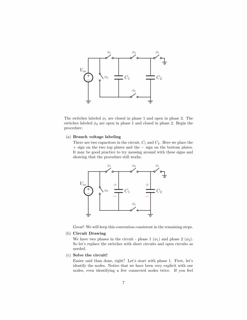
6 Example Circuit 2 - Switched Capacitor
Now we will move on to a slightly more involved example. We’ll see hownicely our procedure works:
6
+
–
φ1
φ1
φ1
φ2
φ2
Vin
C1 C2
The switches labeled φ1 are closed in phase 1 and open in phase 2. Theswitches labeled φ2 are open in phase 1 and closed in phase 2. Begin theprocedure:
(a) Branch voltage labeling
There are two capacitors in the circuit, C1 and C2. Here we place the+ sign on the two top plates and the − sign on the bottom plates.It may be good practice to try messing around with these signs andshowing that the procedure still works.
+
–
φ1
φ1
φ1
φ2
φ2
Vin
C1 C2
+ +
− −
Great! We will keep this convention consistent in the remaining steps.
(b) Circuit Drawing
We have two phases in the circuit - phase 1 (φ1) and phase 2 (φ2).So let’s replace the switches with short circuits and open circuits asneeded.
(c) Solve the circuit!
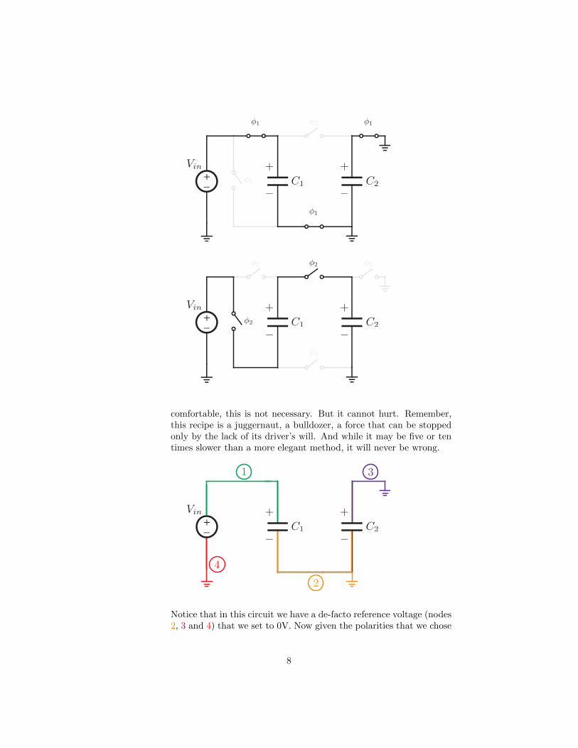
Easier said than done, right? Let’s start with phase 1. First, let’sidentify the nodes. Notice that we have been very explicit with ournodes, even identifying a few connected nodes twice. If you feel
7
+
–
φ1
φ1
φ1
φ2
φ2
Vin
C1 C2
+ +
− −
+
–
φ1
φ1
φ1
φ2
φ2
Vin
C1 C2
+ +
− −
comfortable, this is not necessary. But it cannot hurt. Remember,this recipe is a juggernaut, a bulldozer, a force that can be stoppedonly by the lack of its driver’s will. And while it may be five or tentimes slower than a more elegant method, it will never be wrong.
+
–
Vin
C1 C2
+ +
− −
1
2
3
4
Notice that in this circuit we have a de-facto reference voltage (nodes2, 3 and 4) that we set to 0V. Now given the polarities that we chose
8
earlier, we can find the charges on the + plates of C1 and C2. Justto reiterate, charge is given by capacitance × (V+plate − V−plate)
QC1,φ1= C1 (V1 − V2)
QC1,φ1= C1Vin
QC2,φ1= C2 (V3 − V2)
QC2,φ1= 0
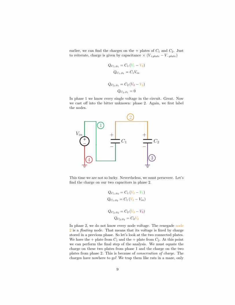
In phase 1 we know every single voltage in the circuit. Great. Nowwe cast off into the bitter unknown: phase 2. Again, we first labelthe nodes.
+
–
Vin
C1 C2
+ +
− −
1
4 3
2
This time we are not so lucky. Nevertheless, we must persevere. Let’sfind the charge on our two capacitors in phase 2.
QC1,φ2 = C1 (V2 − V1)
QC1,φ2= C1 (V2 − Vin)
QC2,φ2= C2 (V2 − V3)
QC2,φ2= C2V2
In phase 2, we do not know every node voltage. The renegade node2 is a floating node. That means that its voltage is fixed by chargestored in a previous phase. So let’s look at the two connected plates.We have the + plate from C1 and the + plate from C2. At this pointwe can perform the final step of the analysis. We must equate thecharge on these two plates from phase 1 and the charge on the twoplates from phase 2. This is because of conservation of charge. Thecharges have nowhere to go! We trap them like rats in a maze, only
9
this maze is of the existential sort that funnels our analysis to thevalues of the voltages in the circuit.
At the node 2 we look at the signs on the attached plates. We havethe + plate of C1 and the + plate of C2. So on the left side of thecharge conservation equation, we will add QC1,φ1 and QC2,φ1 , and onthe right side of the equation, we will add QC1,φ2
and QC2,φ2.
QC1,φ1 +QC2,φ1 = QC1,φ2 +QC2,φ2
C1Vin + 0 = C1 (V2 − Vin) + C2V2
Now we have one equation and one unknown (V2) so we can solve.This leads us to the result:
V2 =2C1
C1 + C2Vin
Yes!
7 Example Circuit 3 - SAR ADC
If the previous circuit wasn’t enough, let’s look at a famous circuit in-troduced in discussion. We can use this circuit in an analog-to-digitalconverter to do what we call a binary search (check wikipedia for SARADC, it’s a very cool circuit). Here we go:
It’s scary, I know. But even in the face of seemingly insurmountable oddsboth you and the recipe will persevere.
(a) Branch Voltage Labeling
This circuit has three capacitors, C1, C2, and C3. As before, we’llplace the + signs on the top plates and the − signs on the bottomplates. And as before, you should try switching the orders of thesesigns around and see if you get the same answer at the end. (Spoileralert: you will.)
(b) Circuit Drawing
Now, in this circuit, we have three phases: 1, 2 and 3. As before, wedraw the circuit in each of the phases replacing the switches by opencircuits or short circuits as needed. Note that if a switch is markedas φ2,3, it simply means that the switch will be closed in phases 2and 3, and open otherwise (in phase 1). Nothing new! :-)
(c) Solve the Circuit!
Remember that we’re not just solving a circuit. We are actually solv-ing three circuits, one for each phase. I’m sure you have a plethoraof curses for the 16A staff fresh on your lips right now. But beforeyou use them, hear us out...
10
+
–Vin
C1 C2 C3
φ1
φ2φ3 φ1 φ1
φ2,3φ1
φ2,3
+
–Vref
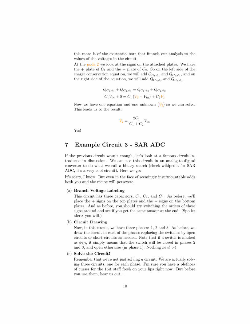
Here’s the circuit for phase 1. As earlier, we have identified all thenodes. Don’t forget the ground node(s)!
Next, we calculate the charges on the + plates of C1, C2 and C3
in terms of the node voltages V1, V2, and V3. Note that V1 = 0,V2 = Vin, and V3 = 0.
Then,QC1,1 = (V1 − V2)C1
givingQC1,1 = −VinC1
andQC2,1 = (V1 − V2)C2
QC2,1 = −VinC2
similarly,QC3,1 = −VinC3
11
+
–Vin
C1 C2 C3
φ1
φ2φ3 φ1 φ1
φ2,3φ1
φ2,3
+
–Vref
+
−
+
−
+
−
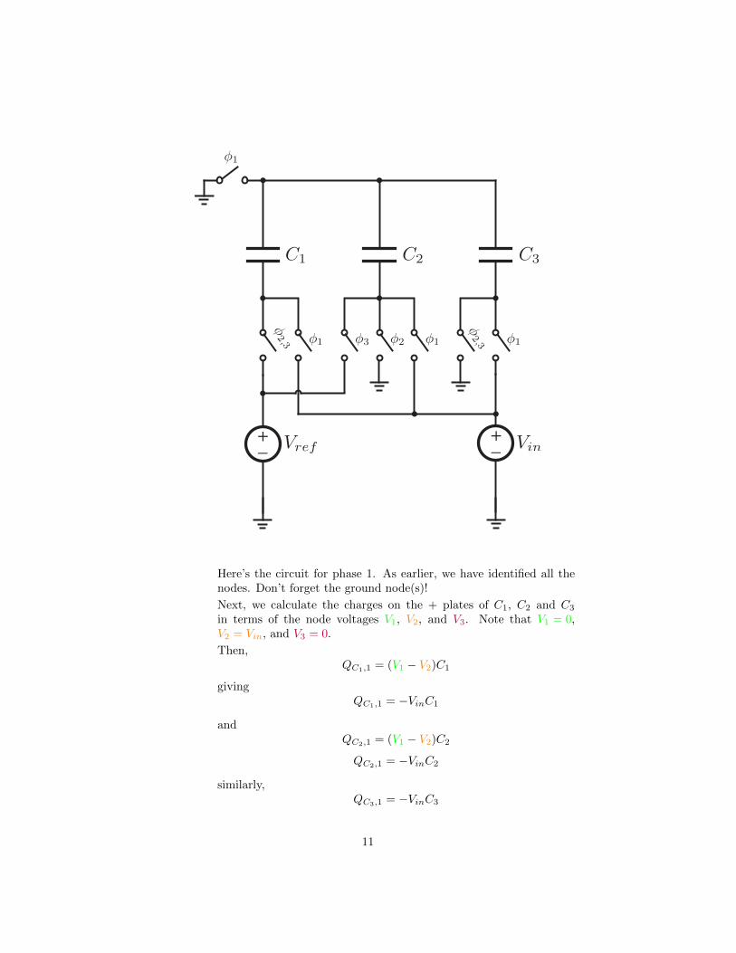
.
Note that all the capacitors are charged to the same voltage, i.e.−Vin, in this phase. You might astutely observe that they are inparallel. If you did not astutely observe this, fear not. You don’tneed to have done so to solve this circuit.
So we know all the voltages and charges exactly in phase 1 (remem-ber, we know Vin). Next up: phase 2! As before, label all the nodesand feel good about yourself. :-)
Note that we have labeled all the ground nodes with the same label,3. We don’t always have to do this but it’s convenient to do so. Notethat V3 = 0, and V4 = Vref . But we do not know V1 in this phase.We finally ran out of luck!
But, we’re intrepid circuit solvers. We don’t give up. Instead, wemove on to the next step. We find the charges across C1, C2 and C3
in phase 2.
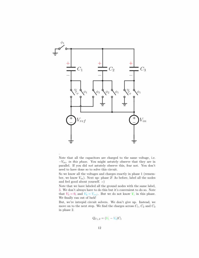
QC1,2 = (V1 − V4)C1
12
+
–Vin
C1 C2 C3
φ1
φ2φ3 φ1 φ1
φ2,3φ1
φ2,3
+
–VrVV ef
+
−
+
−
+
−
QC1,2 = (V1 − Vref )C1
QC2,2 = (V1 − V3)C2
QC2,2 = V1C2
QC3,2 = (V1 − V3)C3
QC3,2 = V1C3
Since we do not know V1 in phase 2, we attempt to solve for it! Todo this, let’s identify where charge is conserved. Note that, in phase2, node 1 is a floating node – which means that the total charge onall the plates connected to it (in this case, the top plates of 1, 2 and3) cannot really go anywhere between phase 1 and phase 2. (Sure,the charges can flow from plate to plate. But ultimately, they are allstill going to be residing somewhere on the green piece of metal that
13

+
–VinVV
C1 C2 C3
φ1
φ2φ3 φ1 φ1
φ2,3φ1
φ2,3
+
–Vref
+
−
+
−
+
−
is part of the circuit. By the way, if you don’t want to be identifyingweirdly colored pieces of metal that charges are going to be trappedin, i.e. if electrons aren’t your thing, worry not. There’s an easierway to identify floating nodes. Any node that is not connected to avoltage source, current source or ground is going to be a floating node.Simply because there will be no source or sink of charge connectedto that node.)
After that little ramble, we soldier on. We say that the total chargeon all the plates connected to node 1 is conserved. This simply meansthat
QC1,1 +QC2,1 +QC3,1 = QC1,2 +QC2,2 +QC3,2
Substituting our expressions for charges in phases 1 and 2 in, we’llget
−VinC1 − VinC2 − VinC3 = (V1 − Vref )C1 + V1C2 + V1C3
14
+
–VinVV
C1 C2 C3
φ1
φ2φ3 φ1 φ1
φ2,3φ1
φ2,3
+
–Vref
+
−
+
−
+
−
giving us
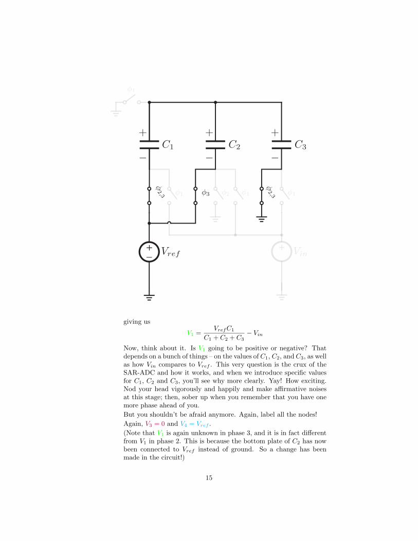
V1 =VrefC1
C1 + C2 + C3− Vin
Now, think about it. Is V1 going to be positive or negative? Thatdepends on a bunch of things – on the values of C1, C2, and C3, as wellas how Vin compares to Vref . This very question is the crux of theSAR-ADC and how it works, and when we introduce specific valuesfor C1, C2 and C3, you’ll see why more clearly. Yay! How exciting.Nod your head vigorously and happily and make affirmative noisesat this stage; then, sober up when you remember that you have onemore phase ahead of you.
But you shouldn’t be afraid anymore. Again, label all the nodes!
Again, V3 = 0 and V4 = Vref .
(Note that V1 is again unknown in phase 3, and it is in fact differentfrom V1 in phase 2. This is because the bottom plate of C2 has nowbeen connected to Vref instead of ground. So a change has beenmade in the circuit!)
15
+
–Vin
C1 C2 C3
+
−
+
−
+
−
1
2
3
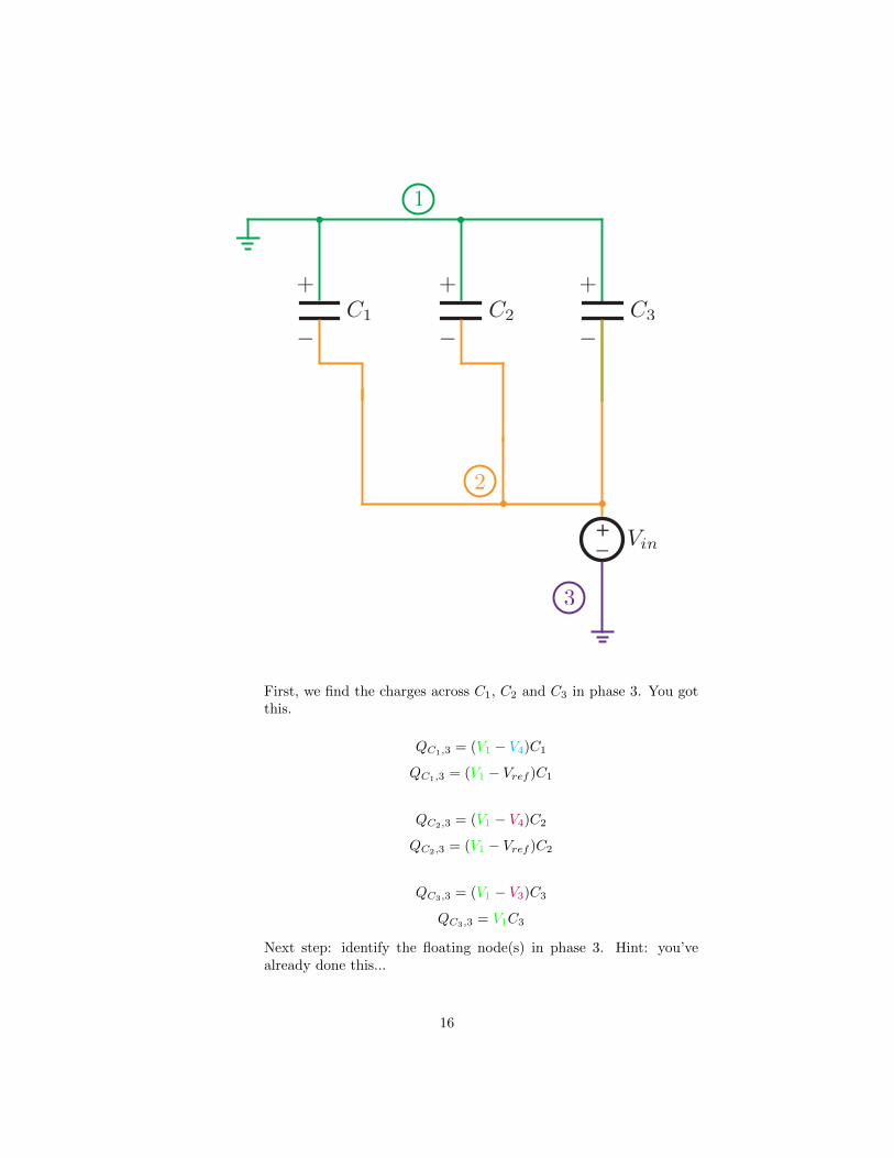
First, we find the charges across C1, C2 and C3 in phase 3. You gotthis.
QC1,3 = (V1 − V4)C1
QC1,3 = (V1 − Vref )C1
QC2,3 = (V1 − V4)C2
QC2,3 = (V1 − Vref )C2
QC3,3 = (V1 − V3)C3
QC3,3 = V1C3
Next step: identify the floating node(s) in phase 3. Hint: you’vealready done this...
16
C1 C2 C3
+
–Vref
+
−
+
−
+
−
1
3
34
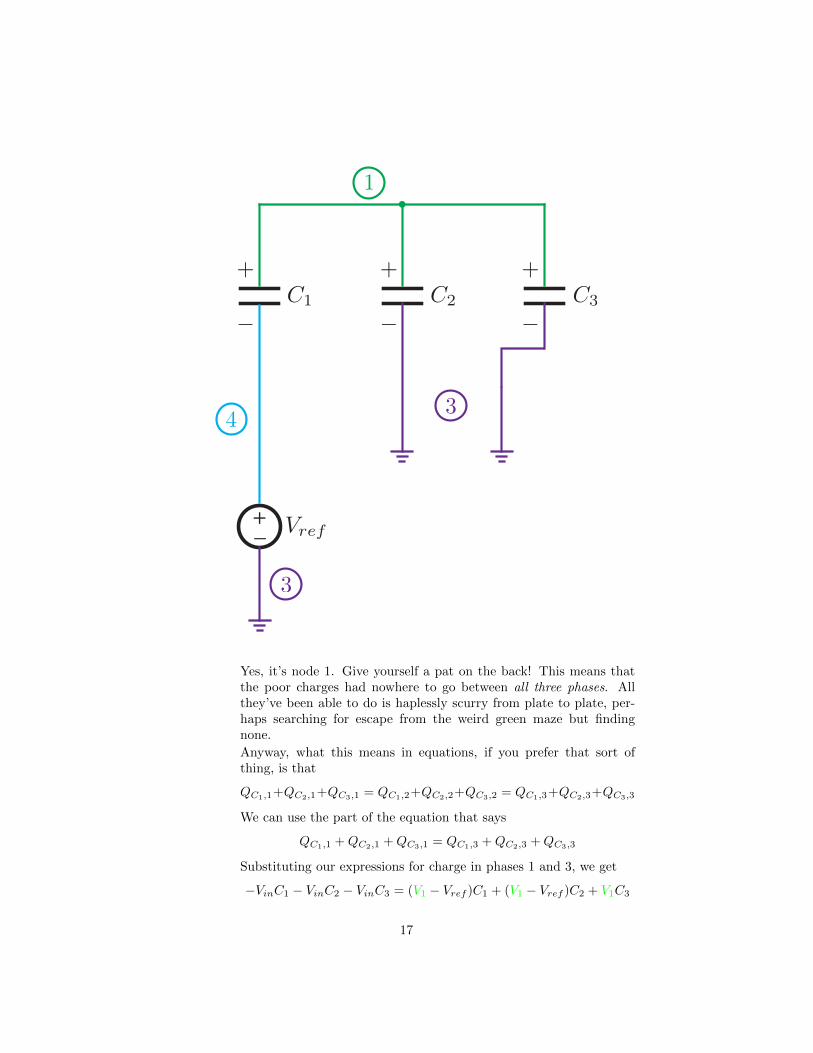
Yes, it’s node 1. Give yourself a pat on the back! This means thatthe poor charges had nowhere to go between all three phases. Allthey’ve been able to do is haplessly scurry from plate to plate, per-haps searching for escape from the weird green maze but findingnone.
Anyway, what this means in equations, if you prefer that sort ofthing, is that
QC1,1+QC2,1+QC3,1 = QC1,2+QC2,2+QC3,2 = QC1,3+QC2,3+QC3,3
We can use the part of the equation that says
QC1,1 +QC2,1 +QC3,1 = QC1,3 +QC2,3 +QC3,3
Substituting our expressions for charge in phases 1 and 3, we get
−VinC1 − VinC2 − VinC3 = (V1 − Vref )C1 + (V1 − Vref )C2 + V1C3
17
C1 C2 C3
+
–Vref
+
−
+
−
+
−
1
4
3
3
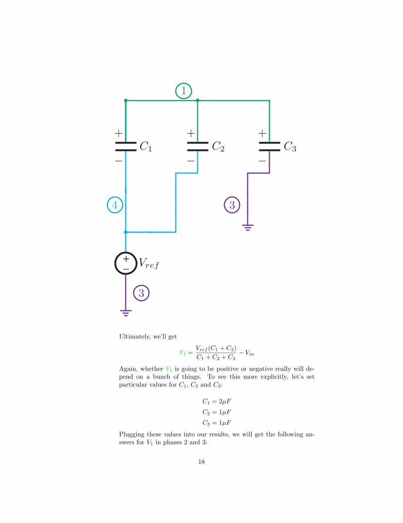
Ultimately, we’ll get
V1 =Vref (C1 + C2)
C1 + C2 + C3− Vin
Again, whether V1 is going to be positive or negative really will de-pend on a bunch of things. To see this more explicitly, let’s setparticular values for C1, C2 and C3:
C1 = 2µF
C2 = 1µF
C3 = 1µF
Plugging these values into our results, we will get the following an-swers for V1 in phases 2 and 3:
18
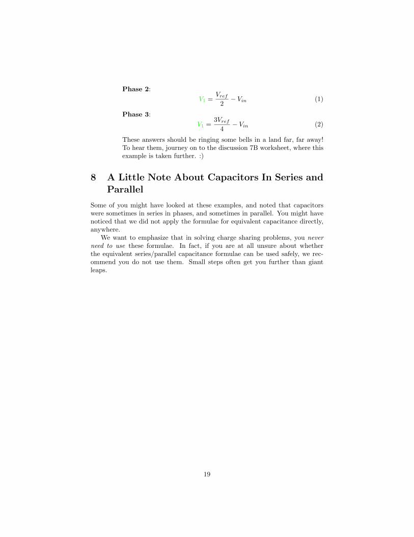
Phase 2:
V1 =Vref
2− Vin (1)
Phase 3:
V1 =3Vref
4− Vin (2)
These answers should be ringing some bells in a land far, far away!To hear them, journey on to the discussion 7B worksheet, where thisexample is taken further. :)
8 A Little Note About Capacitors In Series andParallel
Some of you might have looked at these examples, and noted that capacitorswere sometimes in series in phases, and sometimes in parallel. You might havenoticed that we did not apply the formulae for equivalent capacitance directly,anywhere.
We want to emphasize that in solving charge sharing problems, you neverneed to use these formulae. In fact, if you are at all unsure about whetherthe equivalent series/parallel capacitance formulae can be used safely, we rec-ommend you do not use them. Small steps often get you further than giantleaps.
19