redressing timing issues for speed-independent circuits...
TRANSCRIPT

Microelectronics System Design Research Group
School of Electrical and Electronic Engineering
Redressing Timing Issues for Speed-IndependentCircuits in Deep Sub-micron Age
Yu Li
Technical Report Series
NCL-EEE-MSD-TR-2012-180
July 2012

Contact: ②✉✳❧✐✶❅♥❝❧✳❛❝✳✉❦
NCL-EEE-MSD-TR-2012-180
Copyright c© 2012 Newcastle University
Microelectronics System Design Research Group
School of Electrical and Electronic Engineering
Merz Court
Newcastle University
Newcastle upon Tyne, NE1 7RU, UK
❤tt♣✿✴✴❛s②♥❝✳♦r❣✳✉❦✴
Redressing Timing Issues for
Speed-Independent Circuits in Deep
Sub-micron Age
Yu Li
Faculty of Science, Agriculture and Engineering
Newcastle University
A thesis submitted for the degree of
Doctor of Philosophy
2012 July

1. Reviewer:
2. Reviewer:
Day of the defence:
Signature from head of PhD committee:
ii

Abstract
With continued advancement in semiconductor manufacturing tech-
nologies, process variations become more and more severe. These
variations not only impair circuit performance but may also cause po-
tential hazards in integrated circuits (IC). Asynchronous IC design,
which does not rely on the use of an explicit clock, is more robust to
process variations compared to synchronous design and is suggested
to be a promising design approach in deep-submicron age, especially
for low-power or harsh environment applications.
However, the correctness of asynchronous circuits is also becoming
challenged by the shrinking technology. The increased wire delays
compared to gate delays and threshold variations could bring glitches
into the circuit.
This work proposes a method to generate a set of su�cient timing
constraints for a given speed-independent circuit to work correctly
when the isochronic fork timing assumption is lifted into a weaker
timing assumption. The complexity of the entire process is polyno-
mial to the number of gates. The generated timing constraints are
relative orderings between the transition events at the input of each
gate and the circuit is guaranteed to work correctly by ful�lling these
constraints under the timing assumption.
The benchmarks show that both the number of total constraints and
the constraints that are only needed to eliminate strong adversary
paths are reduced by around 40% compared to those suggested in the
current literature, thus claiming the weakest formally proved condi-
tions.

Acknowledgements
I would like to express my gratitude to my supervisor, Prof. Alex
Yakovlev, for his tremendous help during my Ph.D study. He gave
me freedom when new ideas entered my mind and guided me to the
right way when I was frustrated. His rigorous attitude to research and
diligence to work gave me great encouragement not only in my Ph.D
study but also in my future career.
I would like to thank Dr. Terrence Mak for his education on research
in both technique aspect and non-technique aspect.
I would like to thank Dr. Fei Xia, Dr. Andrey Moknov and Dr.
Danil Sokolov for reading through my thesis and helping me with my
English.
I would like to thank Chao Jin and Liuyang Li for their inspiring
discussion.
I would like to thank my whole group for their help on my life and
for the joy they brought to me.
Especially, I would like to give thanks to my parents. For the incom-
putable hardships they conquered when bring me up.

Contents
List of Figures vi
List of Tables x
1 Introduction 1
1.1 Synchronous and asynchronous circuits . . . . . . . . . . . . . . . 1
1.2 The data path and control path . . . . . . . . . . . . . . . . . . . 6
1.3 Signi�cance of the thesis . . . . . . . . . . . . . . . . . . . . . . . 7
1.4 Organization of thesis . . . . . . . . . . . . . . . . . . . . . . . . . 9
1.5 Publications . . . . . . . . . . . . . . . . . . . . . . . . . . . . . . 10
2 Background 11
2.1 Gate . . . . . . . . . . . . . . . . . . . . . . . . . . . . . . . . . . 11
2.2 Delay models and types . . . . . . . . . . . . . . . . . . . . . . . 13
2.3 Signal and Circuit . . . . . . . . . . . . . . . . . . . . . . . . . . . 14
2.4 Operation modes . . . . . . . . . . . . . . . . . . . . . . . . . . . 15
2.5 Asynchronous control circuits . . . . . . . . . . . . . . . . . . . . 16
2.5.1 Asynchronous design paradigms . . . . . . . . . . . . . . . 16
2.6 Discussions on the delay model of SI circuits . . . . . . . . . . . 20
3 Speed-independent Circuits 23
3.1 Why SI design . . . . . . . . . . . . . . . . . . . . . . . . . . . . . 23
ii
CONTENTS
3.2 Petri Net . . . . . . . . . . . . . . . . . . . . . . . . . . . . . . . . 25
3.3 Signal Transition Graph . . . . . . . . . . . . . . . . . . . . . . . 28
3.4 State Graph . . . . . . . . . . . . . . . . . . . . . . . . . . . . . . 30
3.5 Summary . . . . . . . . . . . . . . . . . . . . . . . . . . . . . . . 33
4 Timing Issues in SI Circuits 34
4.1 Timing assumptions in SI circuits . . . . . . . . . . . . . . . . . . 34
4.2 Existing research on isochronic fork reliability . . . . . . . . . . . 35
4.2.1 Input negations . . . . . . . . . . . . . . . . . . . . . . . . 36
4.2.2 Threshold variations . . . . . . . . . . . . . . . . . . . . . 37
4.2.3 Bu�er insertion . . . . . . . . . . . . . . . . . . . . . . . . 39
4.3 Recent research on isochronic fork relaxation . . . . . . . . . . . . 41
4.4 Summary . . . . . . . . . . . . . . . . . . . . . . . . . . . . . . . 46
5 Hazard checking method 48
5.1 Introduction . . . . . . . . . . . . . . . . . . . . . . . . . . . . . . 49
5.1.1 Overall �ow . . . . . . . . . . . . . . . . . . . . . . . . . . 50
5.2 Deriving the Local STG . . . . . . . . . . . . . . . . . . . . . . . 52
5.2.1 Decomposition of a free-choice STG into MGs . . . . . . . 53
5.2.2 Projecting MG components on operator signals . . . . . . 55
5.3 Timing ordering relaxation . . . . . . . . . . . . . . . . . . . . . . 56
5.3.1 Classi�cation of arcs in the local STG . . . . . . . . . . . . 58
5.3.2 Arc relaxation algorithm . . . . . . . . . . . . . . . . . . . 59
5.3.3 Removing redundant arcs . . . . . . . . . . . . . . . . . . 68
5.4 Local STG relaxation and hazard criterion . . . . . . . . . . . . . 73
5.4.1 Four relaxation cases . . . . . . . . . . . . . . . . . . . . . 73
iii

CONTENTS
5.5 Optimal relaxation order . . . . . . . . . . . . . . . . . . . . . . 81
5.6 Top level algorithm . . . . . . . . . . . . . . . . . . . . . . . . . 84
5.6.1 Complexity analysis . . . . . . . . . . . . . . . . . . . . . 85
5.6.2 Proof of correctness . . . . . . . . . . . . . . . . . . . . . 86
5.7 Delay padding to ful�ll timing constraints . . . . . . . . . . . . . 88
5.8 Summary . . . . . . . . . . . . . . . . . . . . . . . . . . . . . . . 90
6 OR-causality Decomposition 91
6.1 OR-causality . . . . . . . . . . . . . . . . . . . . . . . . . . . . . 91
6.1.1 OR-causality in relaxation case 2 . . . . . . . . . . . . . . 92
6.1.2 OR-causality in relaxation case 3 . . . . . . . . . . . . . . 97
6.2 Decomposition of OR-causality . . . . . . . . . . . . . . . . . . . 100
6.2.1 Generating the solution group . . . . . . . . . . . . . . . . 106
6.2.2 Decomposition according to the solution group . . . . . . . 110
6.3 Summary . . . . . . . . . . . . . . . . . . . . . . . . . . . . . . . 117
7 Results 119
7.1 Design example . . . . . . . . . . . . . . . . . . . . . . . . . . . . 119
7.2 Simulation and Analysis . . . . . . . . . . . . . . . . . . . . . . . 124
7.3 Benchmarks . . . . . . . . . . . . . . . . . . . . . . . . . . . . . . 128
7.3.1 Description of the Tool . . . . . . . . . . . . . . . . . . . . 128
7.3.2 Results . . . . . . . . . . . . . . . . . . . . . . . . . . . . . 131
7.4 Summary . . . . . . . . . . . . . . . . . . . . . . . . . . . . . . . 134
8 Conclusion and Future Work 135
8.1 Conclusion . . . . . . . . . . . . . . . . . . . . . . . . . . . . . . . 135
8.2 Future work . . . . . . . . . . . . . . . . . . . . . . . . . . . . . . 137
iv

CONTENTS
8.2.1 Non-free-choice place . . . . . . . . . . . . . . . . . . . . . 137
8.2.2 Not pure SI circuits . . . . . . . . . . . . . . . . . . . . . . 138
References 141
Index 152
v

List of Figures
1.1 A synchronous circuit and the equivalent asynchronous circuit . . 2
2.1 A logic gate . . . . . . . . . . . . . . . . . . . . . . . . . . . . . . 12
2.2 Pure delay and inertial delay . . . . . . . . . . . . . . . . . . . . . 14
2.3 The Hu�man style asynchronous circuit and the Muller style asyn-
chronous circuit . . . . . . . . . . . . . . . . . . . . . . . . . . . . 18
2.4 A 2-input C-element . . . . . . . . . . . . . . . . . . . . . . . . . 19
2.5 Glitches with respect to delay models . . . . . . . . . . . . . . . . 21
3.1 A PN example . . . . . . . . . . . . . . . . . . . . . . . . . . . . . 26
3.2 PN properties . . . . . . . . . . . . . . . . . . . . . . . . . . . . . 28
3.3 An SI circuit with its STGspec and STGimp . . . . . . . . . . . . . 30
3.4 An STG with its SG . . . . . . . . . . . . . . . . . . . . . . . . . 32
4.1 Glitches caused by inverter delay . . . . . . . . . . . . . . . . . . 36
4.2 Glitch caused by threshold variation . . . . . . . . . . . . . . . . . 38
4.3 Timing di�erence caused by bu�er insertion . . . . . . . . . . . . 40
vi

LIST OF FIGURES
4.4 (a) An SI circuit, (b) the STG corresponding to (a), (c) The SI
circuit with all wires explicitly denoted by signals and (d) the STG
corresponding to (c) when the isochronic fork assumption is removed 43
4.5 Intra operator fork timing assumption . . . . . . . . . . . . . . . 44
4.6 A counter-example . . . . . . . . . . . . . . . . . . . . . . . . . . 44
5.1 The entire �ow of this work . . . . . . . . . . . . . . . . . . . . . 50
5.2 A live and safe free-choice PN (a), and its MG components (b)-(d) 54
5.3 Projection of an STG segment on X and t /∈ X . . . . . . . . . . 56
5.4 An SR-latch with its local STG . . . . . . . . . . . . . . . . . . . 59
5.5 Demonstration of a type (4) arc . . . . . . . . . . . . . . . . . . . 60
5.6 relaxation of arc x∗ ⇒ y∗ in the most general case . . . . . . . . . 61
5.7 un-safeness caused by relaxation . . . . . . . . . . . . . . . . . . . 63
5.8 possible unsafe places after relaxation . . . . . . . . . . . . . . . . 63
5.9 If two cycles have a common vertex l . . . . . . . . . . . . . . . . 64
5.10 Shape of MG that will have an unsafe place < x∗, k∗ >, k∗ ∈ y∗⊲
after relaxing x∗ ⇒ y∗ . . . . . . . . . . . . . . . . . . . . . . . . 66
5.11 Shape of the MG that will have an unsafe place < j∗, y∗ >, j∗ ∈⊳
x∗ after relaxing x∗ ⇒ y∗ . . . . . . . . . . . . . . . . . . . . . . 66
5.12 Gate o has a redundant literal p . . . . . . . . . . . . . . . . . . 67
5.13 redundant arcs due to the relaxation . . . . . . . . . . . . . . . . 68
5.14 Property of shortcut places . . . . . . . . . . . . . . . . . . . . . . 70
5.15 Check for shortcut places using Dijkstra's algorithm . . . . . . . . 72
vii

LIST OF FIGURES
5.16 Illustration of timing conformance. (a) the gate and (b)-(d) local
STGs and the corresponding SGs . . . . . . . . . . . . . . . . . . 74
5.17 Relaxation case 1 . . . . . . . . . . . . . . . . . . . . . . . . . . . 75
5.18 Relaxation case 2 . . . . . . . . . . . . . . . . . . . . . . . . . . . 76
5.19 Relaxation case 3 . . . . . . . . . . . . . . . . . . . . . . . . . . . 77
5.20 Relaxation case 4 . . . . . . . . . . . . . . . . . . . . . . . . . . . 78
5.21 Arc modi�cation in case 2. (a) without OR-causality and (b) with
OR-causality. . . . . . . . . . . . . . . . . . . . . . . . . . . . . . 80
5.22 Preventing the gate entering hazardous state s . . . . . . . . . . . 82
5.23 Di�erent timing constraints due to di�erent relaxation ordering . 83
5.24 Calculate the weight of an arc from STGimp . . . . . . . . . . . . 84
5.25 Padding positions . . . . . . . . . . . . . . . . . . . . . . . . . . 89
6.1 OR-causality in relaxation case 2. (a) the gate and (b)-(f)relaxation
steps . . . . . . . . . . . . . . . . . . . . . . . . . . . . . . . . . . 94
6.2 Candidate clause and transition for OR-causality in relaxation case
2. (a) the gate, (b) and (c) two di�erent STG segments . . . . . . 96
6.3 OR-causality in relaxation case 3. (a) the gate, (b) and (c) two
di�erent STG segments . . . . . . . . . . . . . . . . . . . . . . . . 98
6.4 Candidate clause and transition for OR-causality in relaxation case
3. (a) the gate, (b) and (c) two di�erent STG segments . . . . . . 100
6.5 OR-causality decomposition example. (a) the gate, (b) STG seg-
ment before decomposition and (c)-(g)resulting subSTG segments 102
viii

LIST OF FIGURES
6.6 An OR-causality relation in case 2. (a) the gate and (b) its local
STG segment . . . . . . . . . . . . . . . . . . . . . . . . . . . . . 114
6.7 Decomposition results for the OR-causality relation in Figure 6.6.
(a)-(e) resulting subSTG segments . . . . . . . . . . . . . . . . . . 115
6.8 An OR-causality relation in case 3. (a) the gate and (b) its local
STG segment . . . . . . . . . . . . . . . . . . . . . . . . . . . . . 116
6.9 Decomposition results for the OR-causality relation in Figure 6.8.
(a)-(d) resulting subSTG segments . . . . . . . . . . . . . . . . . 117
7.1 The block diagram and STG speci�cation of FIFO . . . . . . . . . 120
7.2 The implementation STG and circuit diagram of FIFO . . . . . . 121
7.3 The STG relaxation procedure of the gate_0 . . . . . . . . . . . 122
7.4 The current starved delays. (a) controlled delay for rising transi-
tion and (b) controlled delay for falling transition . . . . . . . . . 125
7.5 The trend of error rate as the technology shrinks . . . . . . . . . . 126
7.6 The trend of error rate as the scale increases . . . . . . . . . . . . 127
7.7 The delay penalty . . . . . . . . . . . . . . . . . . . . . . . . . . . 128
8.1 A non-free choice STG and its equivalent free-choice STG . . . . . 139
ix

List of Tables
7.1 List of timing constraints . . . . . . . . . . . . . . . . . . . . . . . 124
7.2 Comparison of the timing constraints . . . . . . . . . . . . . . . . 133
x

Chapter 1
Introduction
As the process shrinks, the traditional synchronous design faces great challenges.
Meanwhile, the asynchronous design exhibits advantages in many important as-
pects, such as the tolerance to process variation and reduced power consumption.
This chapter brie�y compares the advantages and disadvantages of synchronous
and asynchronous designs to illustrate why the asynchronous design suggests a
promising design approach in the near future.
1.1 Synchronous and asynchronous circuits
Digital circuits can be partitioned into combinational logic, in which the output
signals depend only on the current input signals, and sequential logic, in which
the output depends both on current input and the past history of inputs(state
of the circuit). Sequential logic is combinational logic with storage components
(latches).
1

1.1 Synchronous and asynchronous circuits
In synchronous circuits all latches change according to the same periodic global
signal, called the clock. Inputs to latches must be stable before clock events arrive
and all latches change simultaneously when the clock events arrive. Clock is used
to synchronize the data transferring between combinational logic blocks and �lter
out unexpected transient events (called glitches) before the circuit becomes stable.
In contrast, asynchronous circuits do not use the clock. Operation on one latch
is triggered by the events coming from its controller, which communicates with
other controllers by handshake protocols.
......
... ...
...
Controller
1CLK
R1
R2
R3
R4CL1
CL2
CL3
CL4
...
R1CL1
R2 CL2
R3 CL3
R4 R4
(a) (b)
Controller
2
Controller
4
Controller
3
Req
Ack
Req
Ack
Req
Ack
Figure 1.1: A synchronous circuit and the equivalent asynchronous cir-
cuit -
The schematic diagram of a synchronous circuit is shown in the diagram (a)
in Figure 1.1 with the schematic diagram of the equivalent asynchronous circuit
shown in diagram (b). In the synchronous circuit, four registers (R1-R4) are con-
trolled by the clock signal (CLK). The clock cycle period must be greater than
the worst delay of all combinational logic blocks in the circuit and all combina-
tional logic blocks (CL1-CL4) will be synchronized by the end of each clock cycle.
However, in the asynchronous circuit, the clock is not used. The transformations
2
1.1 Synchronous and asynchronous circuits
on the data are synchronized by the handshake signals. Request (Req) will be
sent to the controller of the sink of the data from the source controller when the
data from the source is ready and the acknowledge (Ack) will be sent back to
indicate the completion of the operation.
Thanks to the Moore's law[1], the complexity of the integrated circuit dou-
bles every 18 months. Nowadays, a single chip could contain more than one
billion transistors. Certain problems, which were not quite severe in the last few
decades, are becoming critical today or will be critical in the near future. The
synchronous design, which introduces a global clock to mask glitches and divide
the combinational and sequential logics, has been the mainstream in the digital
integrated circuit community. However, the weakness of synchronous design is
exposed when the semiconductor technology shrinks.
Performance and power :
It is very costly to distribute a global clock signal on a multi-billion transistor
chip. Clock signal skews along the large distribution tree. As the number of
transistors increases and the delay of transistor decreases, the clock skew problem
becomes more and more severe. Additional area or clock magnitude needs to be
sacri�ced in order to guarantee the correctness of the circuit. In addition, the
power consumption related to the distribution clock signal consumes the largest
proportion in a synchronous circuit. Currently, up to 40% of total power is
consumed by the clock distribution network [2] and this situation becomes worse
as the complexity and the frequency of the circuit grows [3].
Meanwhile, although the clock could prevent glitches from causing errors in
synchronous circuits, glitches do dissipate energy. Glitches are useless transi-
3

1.1 Synchronous and asynchronous circuits
tions, which could propagate in the combinational logics and cause additional
transitions. As reported in [4], the power dissipation related to glitches in CMOS
technology consumes up to 15% of total power.
As the feature size of technology shrinks, the process variations become a
new important factor that in�uences the performance of digital circuits. In or-
der to get an acceptable yield, synchronous design needs to set its clock period
conservatively.
Unlike the synchronous design in which glitches could be �ltered out by the
clock, asynchronous circuits are usually vulnerable to glitches. The handshake
protocols cannot distinguish between a real transition and a glitch. Any glitch
could be considered by some logic as a premature transition and causes hazards.
Designers of asynchronous circuits usually put quite a lot of e�ort to avoid danger-
ous races in the circuit. This always results in that asynchronous design consumes
more area and e�orts compared to the synchronous design. Due to the simplicity,
synchronous design dominates the integrated circuit market during past decades.
But, as the mobile electronics devices become the mainstream of the consumer
electronics, the performance and energy dissipation become the two most con-
cerned aspects for industry designs. In contrast, the area now becomes a less
concerned aspect. All those above indicate that asynchronous circuits suggest a
promising design paradigm, which o�ers a high performance and low power con-
sumption solution in the coming decades for both the technical and commercial
reasons.
Modularity :
The circuit design trends to compose a powerful system by many small com-
4

1.1 Synchronous and asynchronous circuits
putational modules or intellectual property (IP) cores, which communicate with
each other through protocols to achieve higher energy e�ciency. Directly con-
necting multiple synchronous modules together is very di�cult if not impossible.
The asynchronous handshake suggests a promising approach to be the interface
protocol to connect sub-modules. As expected by ITRS [5], by 2022, up to 45%
signals of a design will be driven by handshake.
Without doubt, asynchronous circuits will attract more designers' attention in
the coming decades. The inherent request and acknowledgement mechanism can
avoid the clock skew and distribution problem. Also, this mechanism will auto-
matically shut down unused parts in a circuit and avoid generating the unneeded
transitions and thus reduces the power consumption. Di�erent modules could
be easily connected together under protocol based scheme. The strict glitch-free
requirement and the conservative delay assumption makes asynchronous circuits
have much stronger variation tolerance ability compared to the synchronous coun-
terpart.
However, the asynchronous design paradigm also meets challenges.
Without the clock to �lter out glitches, asynchronous circuits su�er from race
hazards[6], which means that circuits might exhibit glitches or even go into the
wrong state depending on di�erences in delay of elements in circuits. In or-
der to avoid race hazards, the synthesis of asynchronous circuits needs to ful�ll
additional requirements. These requirements make asynchronous circuits more
di�cult to design compared with synchronous circuits. Also, the automatic syn-
thesis of asynchronous circuits usually needs to explore the entire state space to
ful�ll the hazard-free requirement and optimize the logic. Asynchronous circuits
5

1.2 The data path and control path
usually exhibit highly concurrency among events. The computation complexity
is in the order of O(2n), with respect to the number of signals (n) in the circuit.
This makes asynchronous circuits hard to design even in moderate size.
Asynchronous circuit design paradigm does not have an entire design �ow
support. The EDA tool support for asynchronous design is poor, not only because
there is no uniformed design paradigm but also the real di�culty behind this
matter. Also, the asynchronous circuit is not only hard to design but also to test.
Due to the problems mentioned above, designing asynchronous circuit al-
ways requires experienced designers. Therefore, the time cost for designing asyn-
chronous circuit is usually much greater than for designing a synchronous one.
Nowadays, the semiconductor technology goes into deep sub-micron age and
the design trends to many-core, low power, environment variation robust and
process variation tolerance applications. These requirements just meet the char-
acteristics of asynchronous circuits.
1.2 The data path and control path
A circuit is typically partitioned into two main parts, the data path and the
control path. The data path usually includes the units to process the data, e.g.
adders and the units for storage and communication e.g. registers. The control
path usually provides signals that control the data path to work properly, e.g. op-
eration codes and the clock signal. In Figure 1.1, the control of the two circuits
includes the clock (CLK) and asynchronous controllers; the datapath includes
registers and the combinational logic. This thesis focuses on controllers in asyn-
6

1.3 Signi�cance of the thesis
chronous circuits (like the controllers 1-4 in diagram (b) in Figure 1.1. Circuits
discussed in this thesis refer to the control circuits if not speci�ed otherwise.
1.3 Signi�cance of the thesis
Among all asynchronous design paradigms, delay-insensitive circuits, which could
tolerate arbitrarily large delay variations on both gates and wires, show the
strongest process variation tolerance ability. However, delay-insensitive circuits
have been proved to be quite limited that only a very small set of speci�cations
have a delay-insensitive implementation[7]. This also indicates that for almost all
useful speci�cations, the implementations should contain some timing assump-
tions in them. Speed-independent circuits, which only take the isochronic fork
timing assumption, are supposed to be the paradigm that imposes the weakest
timing assumption. Speed-independent circuits could work correctly under many
harsh situations, e.g. VDD variations and the gate delay variations. However, the
other variations like the threshold variation could still cause speed-independent
circuits to malfunction.
Speed-independent circuits suggest a good starting point to correctly imple-
ment circuit under unprecedented variations. Unlike the design paradigms that
introduce the real time information in synthesis, speed-independent circuits only
compare the arriving orders of events. They therefore redress only those timing
issues needed to guarantee the required orders. This is desirable in the deep sub-
micron age. The delay variations are quite large that estimating the exact time
is di�cult and unreliable in the deep submicron age. However, orders between
7

1.3 Signi�cance of the thesis
two events are much easier to predict and �x. Currently, most layout tools does
not directly support relative timing constraints. This is because the synchronous
design is widely adopted by the industry and synchronous tool is well developed
where the numerical delay is used. However, the layout tool for the asynchronous
design that supports the relative timing constraints could be developed as the
asynchronous design becomes more and more important.
The veri�cation of the timing ful�llment is a very di�cult and time consuming
task. The time complexity usually reaches the exponential or even double expo-
nential order with respect to the number of signals in a circuit. This is hardly
acceptable even for a moderate scale circuit.
This thesis proposes an e�cient method to verify and re-synthesize speed-
independent circuits. It takes a reasonably weaker timing assumption compared
to the isochronic fork timing assumption and then introduces a series of algo-
rithms to verify circuit and generate a set of su�cient timing constraints to
guarantee the correctness of the circuit. The generated timing constraints could
always be ful�lled.
The main contributions of this thesis are:
1) It corrects some wrong conclusions given by previous researchers about the
weakest timing assumption in speed-independent circuits.
2) It introduces a hazard checking criterion for speed-independent circuits
when the isochronic fork timing assumption is relaxed.
3) Most importantly, this thesis proposes a method utilizing properties of the
speed-independent circuit to do the timing veri�cation in polynomial time. This
method divides the entire veri�cation problem into smaller sub-problems and thus
8

1.4 Organization of thesis
avoids exploring the full state space.
The limitation of this thesis is that in the point 3) mentioned above, one
operation "projecting a Petri Net on a subset of transitions" is needed. However,
this is an open question for general Petri Nets. Thus, the input signal transition
graph to this technique (one kind of Petri Net) is limited to a free-choice Net,
where Hack's algorithm[8] could apply.
1.4 Organization of thesis
This thesis is organized as follows:
Chapter 1 brie�y introduces the synchronous and asynchronous design and
presents the signi�cance of this thesis.
Chapter 2 de�nes the terms used in asynchronous community and introduces
di�erent asynchronous design paradigms.
Chapter 3 introduces the related descriptions and models of speed-independent
circuits, which will be used in the following chapters and explains why speed-
independent circuits are adopted by this thesis among asynchronous design paradigms.
Chapter 4 investigates the possible situations that could cause failures of the
isochronic fork and discusses the technology trends that a�ect these situations.
Also, related research is overviewed in this chapter.
Chapter 5 presents the main method for hazard checking when the funda-
mental timing assumption of speed-independent circuits is relaxed.
Chapter 6 analyzes one complex problem, the OR-causality, which may occur
during the hazard checking process presented in Chapter 5 in detail and proposes
9
1.5 Publications
a technique to solve this problem.
Chapter 7 presents the benchmark results of the method. This chapter com-
pares the tightness of the generated timing constraints with similar research. Also
one design example is presented in detail to demonstrate the proposed method
and to show the penalty introduced by eliminating the potential hazards.
Chapter 8 concludes the thesis and discusses the possible ways to break
the limitations of the proposed method to make it suitable for broader range of
speci�cations.
1.5 Publications
The main results of the thesis have been published in the following paper:
• "Relative Timing Applied to Asynchronous Circuit Synthesis and Decom-
position" (19th UK Asynchronous Forum)
• "Conditions and Techniques for Correctness of SI/QDI Circuits Under Large
Variability" (21st UK Asynchronous Forum)
• "Redressing timing issues for speed-independent circuits in deep submicron
age" (DATE'11)
10

Chapter 2
Background
This chapter gives the de�nitions of basic elements and concepts of a digital
circuit and also introduces popular asynchronous design paradigms.
2.1 Gate
Gates are basic elements in a circuit. In this thesis, a gate is de�ned as an n
inputs and one output boolean variable. If the inputs contain its output variable,
the gate is sequential, otherwise it is combinational. For every gate there is an
associated logic function f to compute it.
The de�nition of logic function in [9] is adopted.
A logic function f with n input variables is a mapping f : {0, 1}n 7→ {0, 1},
where {0, 1}n is a binary vector over its input variables called input state. The
set of input states that maps to ′1′ is the on-set of f , while that maps to ′0′ is its
o�-set .
11

2.1 Gate
A literal is a variable x or its complement x. A cube c is a set of literals
on di�erent variables, which means that literal x cannot appear multiple times
and x and x cannot appear simultaneously in a cube. A cube c represents the
vertexes corresponding to the boolean product of its literals. A cube c′ is covered
by another cube c′′ if c′′ ⊆ c′, denoted by c′ ⊑ c′′.
A cube is an implicant of a logic function f if it does not cover any vectors in
o�-set of f . An implicant of f is called a prime implicant if it cannot be covered
by any other implicants of f . A cover U is a set of cubes, which represents the
boolean sum of its cubes. A cover U is an on-set cover of logic function f if each
cube in U is an implicant of f and each vertex in f is covered by at least one cube
in U . A cover D is an o�-set cover of logic function f if D is an on-set cover of f ,
where f is a logic function obtained by exchanging the on-set and o�-set of f . A
cover U is a prime cover of logic function f if all its cubes are prime implicants of
f . A cube c is redundant in a cover D of logic function f , if D\c is still a cover of
f . A cover D is redundant for f if at least one cube in it is redundant, otherwise
it is irredundant. An irredundant prime cover of logic function f is denoted by
f↑ and an irredundant prime cover of f if denoted by f↓. Each cube in f↑ and f↓
is called a clause. The notation fa↑ and fa↓ is used if f computes gate a.
ab
c
Figure 2.1: A logic gate -
12
2.2 Delay models and types
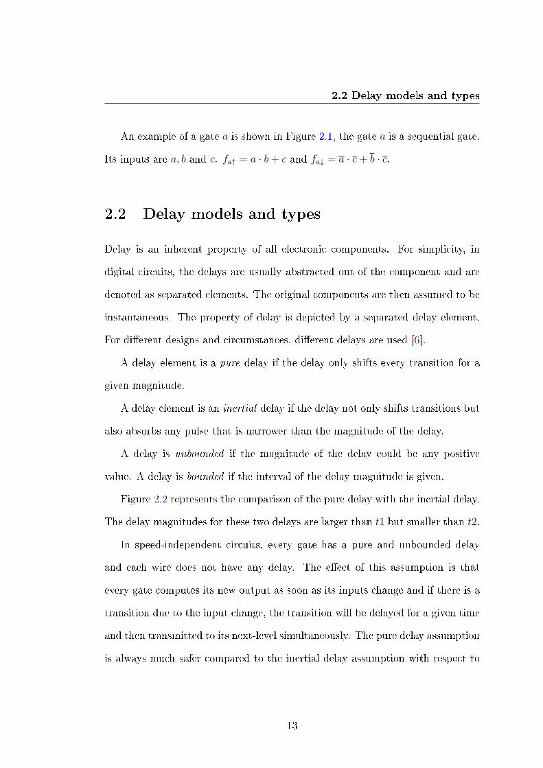
An example of a gate a is shown in Figure 2.1, the gate a is a sequential gate.
Its inputs are a, b and c. fa↑ = a · b+ c and fa↓ = a · c+ b · c.
2.2 Delay models and types
Delay is an inherent property of all electronic components. For simplicity, in
digital circuits, the delays are usually abstracted out of the component and are
denoted as separated elements. The original components are then assumed to be
instantaneous. The property of delay is depicted by a separated delay element.
For di�erent designs and circumstances, di�erent delays are used [6].
A delay element is a pure delay if the delay only shifts every transition for a
given magnitude.
A delay element is an inertial delay if the delay not only shifts transitions but
also absorbs any pulse that is narrower than the magnitude of the delay.
A delay is unbounded if the magnitude of the delay could be any positive
value. A delay is bounded if the interval of the delay magnitude is given.
Figure 2.2 represents the comparison of the pure delay with the inertial delay.
The delay magnitudes for these two delays are larger than t1 but smaller than t2.
In speed-independent circuits, every gate has a pure and unbounded delay
and each wire does not have any delay. The e�ect of this assumption is that
every gate computes its new output as soon as its inputs change and if there is a
transition due to the input change, the transition will be delayed for a given time
and then transmitted to its next-level simultaneously. The pure delay assumption
is always much safer compared to the inertial delay assumption with respect to
13

2.3 Signal and Circuit
input
pure delay
inertial delay
t1 t2
Figure 2.2: Pure delay and inertial delay -
glitch-freedom as will be analyzed in the following section.
2.3 Signal and Circuit
Transitions on signals represent the dynamics of a circuit. The set of signals
should depict the entire reachable states of a circuit. Here, we de�ne the signals
of a circuit (denoted by the set A) to be the union of the primary input variables
and gate variables. For circuits which are in context with their environment
(ENV ), the signals coming from the primary inputs are denoted by a set I, the
gate variables which feedback to the ENV are primary outputs denoted by a
set O and the gate variables that are not primary outputs are internal signals
denoted by a set R. For autonomous circuits, we have I = O = ∅ and R = A.
A circuit is de�ned as a pair C = (A,ϕ), where A is a set of signals and ϕ is
a labeling function which labels a wire between each signal a ∈ I ∪ R and each
fan-out of a.
14
2.4 Operation modes
In the de�nition above, only input signals and gate variables are used to de-
scribe the dynamics of a circuit, wires will not be shown explicitly. This is because
the type of the asynchronous circuit under discussion is the speed-independent
circuit, where wires could be considered to have zero delays, the dynamics of
wires could be fully represented by the gate behaviors. When the isochronic fork
is relaxed (as will be speci�ed in the following chapters), we will still use tech-
niques to avoid introducing signals to wires. The reason behind this is as follows.
Firstly, the number of wires is always equal to or more than the number of gates
in a circuit, so encoding using wire signals would increase the computational com-
plexity. Secondly, introducing signals to wires will break some properties that are
necessary for us to model the behavior of speed-independent circuits (will break
the safeness of a PN).
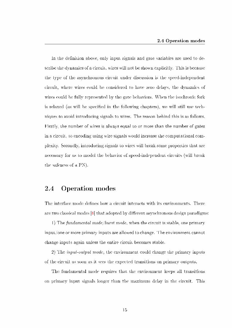
2.4 Operation modes
The interface mode de�nes how a circuit interacts with its environments. There
are two classical modes [6] that adopted by di�erent asynchronous design paradigms:
1) The fundamental mode/burst mode, when the circuit is stable, one primary
input/one or more primary inputs are allowed to change. The environment cannot
change inputs again unless the entire circuit becomes stable.
2) The input-output mode, the environment could change the primary inputs
of the circuit as soon as it sees the expected transitions on primary outputs.
The fundamental mode requires that the environment keeps all transitions
on primary input signals longer than the maximum delay in the circuit. This
15

2.5 Asynchronous control circuits
requires designer to estimate the real delays in a circuit. While input-output mode
requires that every signal transition is acknowledged to make sure that when the
environment sees the expected transitions on primary outputs, all internal signal
transitions have happened.
2.5 Asynchronous control circuits
The class of asynchronous circuits is a very broad class. Di�erent researchers of-
ten propose quite di�erent design �ows, where di�erent speci�cation formalisms,
various assumptions, synthesis techniques and manpower are utilized. This sec-
tion will focus on the introduction of popular asynchronous design methods and
their trade-o�s. Circuits discussed in this section refer to the control circuits if
not speci�ed otherwise. Also, methods referred in this thesis are mainly related
to the design of control. The datapath usually contains a large number of signals
in high concurrency. Techniques that focus on the control are usually not capable
of handling datapath and the synthesized circuits would be ine�cient. However,
a large body of research exists for datapath circuits as well[10] [11] [12].
2.5.1 Asynchronous design paradigms
The Hu�man style asynchronous circuits : The Hu�man style asynchronous cir-
cuits are �rst proposed in [13], which take the bounded wire and gate delay model
and operate under the fundamental mode. The schematic diagram of the Hu�man
style asynchronous circuits is shown in Figure 2.3 (a).
16

2.5 Asynchronous control circuits
The speci�cation of the fundamental mode Hu�man style asynchronous cir-
cuits is often a Hu�man �ow table which represents an asynchronous �nite state
machine (ASFM). The circuit consists of primary input signals (a, b, c in Fig-
ure 2.3 ), primary output signals (x, y, z ), state signals (feedback signals from
output to input, M, N, m, n) and the combinational part of the circuit. In the ini-
tial state, one input of the circuit is allowed to change. Then the combinational
part of the circuit starts to compute the new output value and the next state
value. When the environment receives the new output value, it cannot provide
a new input transition until the circuit becomes stable after receiving the next
state value.
The Hu�man style asynchronous circuits, which are quite similar to the syn-
chronous circuits, are easier to design compared to those in other design methods.
But this kind of circuits has two limitations. Firstly, the operations of the circuit
must follow a strict order that one input must change �rst followed by the state
signals and the output signals. Therefore, concurrency between the input changes
and output changes is not allowed (also the �nite state machine cannot depict
this kind of concurrency). Secondly, delays or other techniques must be used to
guarantee that the next state value cannot propagate to the combinational part
too early and the environment does not provide a new input transition too early.
The fundamental mode Hu�man style asynchronous circuits have the limita-
tion that only one input could change at one time. The early work related to the
synthesis of fundamental mode Hu�man style asynchronous circuit is presented
in [13] [14]. Steven Nowick proposed a burst mode Hu�man style asynchronous
paradigm in [15], which expanded the concurrency to allow a constrained set of
17

2.5 Asynchronous control circuits
input signals (input burst) to change concurrently. However, the burst mode
asynchronous circuits still do not allow the concurrencies between input bursts
and output bursts and still require the timing constraints in the fundamental
mode. The synthesis of the burst mode asynchronous circuits is automated in
the tool MINIMALIST[16].
The burst mode design style is further expanded by Yun and Dill into the
extended burst mode design style[17][18], which allows an input signal to change
concurrently with output signal and allows control �ow to depend on the input
levels. With these extensions, the burst mode design style covers a wide spectrum
of sequential ranging from asynchronous to synchronous. The extended burst
mode speci�cation could be synthesized by the 3D synthesis tool [19].
Environment
Huffman style
asynchronous
circuit
Muller style
asynchronous
circuit
a
Environment
bc
xyzMN
mn
abc
xyz
(a) (b)
Figure 2.3: The Hu�man style asynchronous circuit and the Muller style
asynchronous circuit -
The Muller style asynchronous circuits : Unlike the Hu�man style asynchronous
circuits, the Muller style circuits do not put so many restrictions on speci�cations
and the environment. The schematic diagram of the Muller style circuit is pre-
sented in Figure 2.3 (b). The operation of the circuit is based on the following
18

2.5 Asynchronous control circuits
protocol: the environment is allowed to provide new inputs as soon as it sees ex-
pected outputs. Also, the speci�cation of Muller style circuits does not constraint
the concurrency between signals. The design of input-output mode Muller style
asynchronous circuits was introduced in [20] [21].
The Delay-Insensitive (DI) circuits :
The DI circuits are one kind of Muller style asynchronous circuits that work
correctly even if every wire and gate has unbounded delay. A very important type
of gate in DI circuits is a C-element. The symbol and the truth table of a 2-input
C-element is shown in Figure 2.4. A more general de�nition for C-element is that
output changes if and only if all of its inputs change. So, an inverter is also a
1-input C-element. Among all asynchronous design paradigms, only DI circuits
do not have any timing assumption. So, DI circuits could tolerate arbitrary delay
variations on their components.
But as was proved in [22], the DI circuits are quite limited: if an autonomous
DI circuit is built of single output gates, then all gates must be C-elements.
Moreover, the C-element itself does not have a DI implementation built of basic
gates[23].
C
a
b
c
a b c
0 00 1
1 01 1
0c
c1
n-1
n-1
Figure 2.4: A 2-input C-element -
The Speed-Independent (SI) circuits :
19

2.6 Discussions on the delay model of SI circuits
The DI circuits are quite limited and most practical speci�cations do not have
DI implementations. The SI circuits are usually adopted to enlarge speci�cations
that could be synthesized. As was proved in [24], there exists an SI implemen-
tation for any deterministic computation1. The SI circuits also allow unbounded
delays on gates, but wires in a fork must have the same magnitude delay. If the
delays on wires in a fork (since they have the same magnitude) are combined
into the corresponding gate delay, the timing assumption behind the SI circuits
is equal to say that gates in an SI could have unbounded delays but wires are
instantaneous.
2.6 Discussions on the delay model of SI circuits
Glitches are unwanted transitions on a signal often generated by the delay vari-
ations on gates and wires. Synchronous circuits could use the clock to �lter the
glitches to prevent them from causing hazards. While in asynchronous circuits,
especially for the circuits in input-output mode, all signals should be valid at any
time and therefore any glitch could be recognized as a pre-mature transition.
The appearances of glitches are usually dependent on the delay model. The
pure delay is usually considered to be a safer delay model compared to the inertial
delay, because potential glitches might be absorbed by an inertial delay if they are
narrow enough. But in [26], the author exempli�es that a circuit might manifest a
1Even though the Quasi Delay Insensitive (QDI) circuits [25] have di�erent de�nition, spec-i�cation form and synthesis �ow, they behaviorally equal to the SI circuits. In this thesis, theQDI circuits are indistinguishably recognized as the SI circuits.
20

2.6 Discussions on the delay model of SI circuits
hazard under inertial delay model while it would be safe under pure delay model.
One example of this situation is presented in Figure 2.5, where gate x is an
internal gate and gate y is a primary output. There are two glitches appear on
the two inputs a and b. The output of gate y is expected to stay at '1'. Assume
the gate y has a pure delay. If the delay model of gate x is pure (case 1 in
Figure 2.5), then the glitch on input a will be canceled out by the glitch on gate
x, the primary output y is hazard-free. However, if the gate x has an inertial
delay (the gate y is still under pure delay model) then the glitch on input a will
go through y and appear at the primary output as a hazard(case 2 in Figure 2.5).
y
x
'0'a
glitches
a
b'1'
x
b
y
x
y
case1:
x pure delay
y pure delay
case2:
x inertial delay
y pure delay
Figure 2.5: Glitches with respect to delay models -
The above example shows that the pure delay model is not always safer than
the inertial delay model. But it is only true when one glitch is used to cancel
out another glitch. When we discuss the glitch-free implementation (no glitches
21

2.6 Discussions on the delay model of SI circuits
are allowed at any signal), the pure delay model will always be a safer mode
compared with the inertial delay model.
22

Chapter 3
Speed-independent Circuits
The class of asynchronous circuits is a broad class. Usually, each design paradigm
has its own �ow. This chapter further explains why SI design is more interesting
than other asynchronous design paradigms. Also, this chapter introduces the
mathematical models used in the SI design �ow.
3.1 Why SI design
As was introduced in the previous chapter, there are many asynchronous design
paradigms. Unfortunately, these paradigms have totally di�erent design �ows.
Synthesis techniques for one kind of design cannot be used in others. In this
thesis we adopt the SI design, which we think has the following advantages over
others:
Strong variation tolerance ability :
The SI design which only has an isochronic fork timing assumption is robust
23

3.1 Why SI design
to process variations and harsh environment.
As the technology develops, process variations become quite severe. The de-
sign paradigms that need to evaluate the real timing or compare the relative
timing between similar components become unreliable. Moreover, all kinds of
unreliable environments could appear as the portability of devices increases. The
power supply might be from the energy harvesting devices and/or the circuit it-
self might operate under subthreshold voltage. The SI design has been proved
to adjust well to the harsh environment, while other design paradigms are more
vulnerable to variations.
As will be shown in the following chapters, the isochronic fork timing assump-
tion could be safely relaxed into a much looser timing assumption and this timing
assumption is easier to implement. The overhead to �x the potential hazards is
not expensive.
Comparatively well supported by EDA tools :
One critical obstacle to asynchronous design for general use is the lake of
EDA tool support. Many commercial circuits like [27] and [28] involve remarkable
manual e�orts. Compared with other asynchronous design paradigms, SI design
is comparatively well studied and better supported by EDA tools in the design
�ow. For example, there are [29] [30] [31] [32] [33] and [34] for synthesis. [35] [36]
[37] and [38] for decomposition and technology mapping, [39] [40] [41] and [42]
for veri�cation and [43] for testing. Almost each step in design �ow is supported
or partially supported by existing automation techniques.
24

3.2 Petri Net
3.2 Petri Net
Petri net was �rst formally introduced by Carl Adam Petri in his Ph.D. the-
sis [44] as a modeling language for discrete distributed systems. It has strict
mathematical de�nition and semantics as well as visually graphic representation.
The explicit representations of enabling, disabling, concurrency and con�ict make
Petri Net quite suitable to model asynchronous systems. Especially, one partic-
ular subset of interpreted Petri Net, called the Signal Transition Graph is quite
popular in describing the behavior of SI circuits. Formally,
A Petri Net (PN) is a quadruple N = (P, T, F,m0), where
P is a �nite set of places ,
T is a �nite set of transitions ,
F ⊆ (P × T ) ∪ (T × P ) is a �ow relation and
m0: P → N is the initial marking.
Places represent conditions and are usually depicted as circles (©) in graphical
representation and transitions are events in a system and usually denoted by
bars (−). A place p ∈ P (transition t ∈ T ) is an input place (transition) of a
transition t ∈ T (place p ∈ P ) if p × t ∈ F (t × p ∈ F ) or is an output place
(transition) of a transition t (place p) if t× p ∈ F (p× t ∈ F ). The set of input
places (transitions) of a transition t (place p) is denoted by •t (•p) and the set of
output places (transitions) of a transition t (place p) is denoted by t• (p•). This
de�nition also applies to a set of places (transitions). For example, for the set of
places P1 ⊆ P , •P1 =⋃
p∈P1
•p.
The marking of a PN is a function M : P → N, which gives each place a
25

3.2 Petri Net
non-negative integer representing the number of tokens in this place. A place p
is marked if M(p) > 0, otherwise it is blank. Graphically, a token is drawn as a
dot (•).
A transition t is enabled in a marking m, if every place in •t is marked. An
enabled transition may �re, which will remove one token in each place in •t and
add one token to each place in t•. This �ring will change the marking m into a
new marking m′ and this transformation is denoted by mt−→ m′.
A marking m′ is said to be reachable from marking m, if there exists a �ring
sequence σ : t1t2. . . tn which transforms the marking m to m′. The marking set
M of a PN is the set of all markings reachable from the initial marking m0.
p1
t1
t2 t3
t4
p2 p3
p4 p5
p1
t1
t2 t3
t4
p2 p3
p4 p5
Figure 3.1: A PN example -
The PN example in the left diagram in Figure 3.1 has �ve places P =
{p1, p2, p3, p4, p5}, four transitions T = {t1, t2, t3, t4} and the initial marking m0 =
(1, 0, 0, 0, 0). t1 is the only transition that is enabled in the initial marking. When
it �res, the initial marking transfers into another marking m1 = (0, 1, 1, 0, 0) as
is shown in the right diagram in Figure 3.1. The marking set of this PN is
26

3.2 Petri Net
{(1, 0, 0, 0, 0),(0, 1, 1, 0, 0),(0, 0, 1, 1, 0),(0, 1, 0, 0, 1),(0, 0, 0, 1, 1)}.
Besides the basic semantics of the PN, the properties and concepts [45] intro-
duced below are often involved when certain kinds of PN are used to depict the
behavior of asynchronous circuits.
A transition t is said to be live in a marking m, if there exists a marking m′
reachable from m, such that t is enabled in m′. A PN is live if every transition is
live in any reachable marking from the initial marking m0.
A PN is safe if each place could have at most one token in any reachable
marking from the initial marking m0.
A place is said to be a choice place [46] if it has more than one output transi-
tion. A place is said to be a merge place if it has more than one input transition.
A choice place is further a free-choice place if this place is the only input place of
all of its output transitions. A PN is a free-choice PN if all its choice places are
free-choice places. A PN is said to be a Marked Graph (MG) if it does not have
any choice and merge place.
Two transitions t1 and t2 are in con�ict , if there is a marking m, where t1
and t2 are enabled but �re one will make another from enabled to disabled in the
resulting marking. t1 and t2 are concurrent if for all markings, where t1 and t2
are both enabled, they are not in con�ict.
The PN shown in the left diagram of Figure 3.2 is neither live nor free-choice.
The transition t3 will never be enabled and it has two choice place p2 and p3 as
its input places. The PN shown in the middle diagram of Figure 3.2 is not safe
because every place in it could have up to two tokens; the transitions t1 and t3
are concurrent in this net. Finally, the PN in the right diagram of Figure 3.2 is
27

3.3 Signal Transition Graph
p1
t2
t3
t4
p2 p3
t1
p1 p2
p3 p4
t1
t2
t3
p2 p3
p4
p1
t1 t2
t3 t4
Figure 3.2: PN properties -
live, safe and free-choice and the transitions t1 and t2 are in con�ict.
A transition t1 (t2) is a predecessor transition (successor transition) of tran-
sition t2 (t1), if t•1 ∩• t2 6= ∅ and denoted by t1 ⇒ t2. The set of predecessor
transitions (successor transition) of transition t is denoted by ⊳t(t⊲).
3.3 Signal Transition Graph
The signal transition graph, which is an interpreted PN, was introduced in [47]
(called Signal Graph) and [48] as a high level description of asynchronous cir-
cuits. The transitions in the underlying PN are signal transitions in the circuit.
Formally,
A Signal Transition Graph (STG) is a triple G = (N,A, λ), where
N is the underlying PN,
A is a �nite set of signals and
λ is a labeling function which assigns transitions in N to A× {+,−}.
For all a ∈ A, a+ depicts a rising transition (from logic low to logic high) on
28
3.3 Signal Transition Graph
signal a, a− depicts a falling transition (from logic high to logic low) on signal
a and a∗ is used to depict either a+ or a−. The index i (like a ∗ /i) is used
to distinguish multiple occurrences of transitions on the same signal in an STG
when necessary.
As a special kind of PN, STG inherits all the semantics belonging to PN.
Moreover, in order to model the SI circuits, STG needs ful�lling additional re-
quirements.
Usually, STG is produced by the designer either manually from text descrip-
tion, or by translating the timing diagram with some automatic tools [49]. The
STG, whose signal set A = I∪O, which only depicts the interactions between the
circuit and the environment, is called a speci�cation STG , denoted by STGspec;
while the STG, whose signal set A = I ∪ R ∪ O that depicts all event orders in
an SI circuit, is called an implementation STG , denoted by STGimp.
The PN containing non-free-choice places or unsafe places could be very com-
plex for analyzing. In this thesis, the underlying PN of an STG is restricted
to be live, safe and free-choice if not speci�ed. One technique to process some
non-free-choice STGs will be discussed in the last chapter of this thesis.
Graphically, STG is often short-handed by omitting the places which have
only one input and output transitions and using labeled transitions to instead
the bars in the underlying PN. Figure 3.3 shows an SI circuit (left), in which,
I = {a, b, c}, R = {d} and O = {x, y}. Its STGspec (middle) only depicts the
signal transitions on circuit's interface while its STGimp (right) depicts all the
signal transitions within the circuit.
In an STG, the transitions on the same signal must have consistency . It means
29

3.4 State Graph
that in any �ring sequences, the rising transitions and falling transitions on the
same signal must appear alternatively.
ab
c
d x
y
a+ b+
x+
c+
b-
a-
y+y-
c-
x-
a+ b+
x+
c+
b-
a-
y+
y-
c-
x-d+
d-
SI circuit STG STGspec imp
Figure 3.3: An SI circuit with its STGspec and STGimp -
3.4 State Graph
An STG explicitly describes the relations between events. So, the STG is suitable
for high level modeling and manipulating the behavior of an asynchronous system.
While, the logic synthesis, optimization and veri�cation are much easier to be
carried on a low level model, where the reachable states of an STG are explicitly
presented.
The state graph (also called the transition diagram in [47] or state transition
diagram in [9]) is a binary labeled �nite automaton. Each state in the �nite au-
tomaton is a reachable marking of its STG. The binary value of a state represents
the value of signals in the corresponding circuit.
A state graph (SG) is a quintuple SG = (A, S,E, π, s0), where
30

3.4 State Graph
A is a �nite set of signals,
S is a set of states,
E = S × S is a set of transitions,
π is a labeling function which labels each state s ∈ S with a bit-vector over
A and
s0 is the initial state.
The value of signal a in state s is denoted by s(a). Two states s and s′ are
adjacent if (s, s′) ∈ E. A transition from state s to its adjacent state s′ by �ring
a∗ is denoted by sa∗−→ s′. For s
a∗−→ s′ the triple (s, a∗, s′) is said to be consistent
if when a∗ = a+ then s(a) = 0, s′(a) = 1 and s(b) = s′(b) for all b ∈ A and b 6= a.
An SG is considered to have a consistent state encoding if each possible triple
(s, a∗, s) in this SG is consistent.
An SG of an STG could be derived by recursively �ring enabled transitions
from the initial marking and labeling the resulting marking set. An SG derived
from an STG will have a consistent state encoding if and only if the rising and
falling transitions on the same signal appear iteratively[48] in the STG.
The concept of region used data mining was introduced into the SG in [50] for
classifying the states in order to accelerate the manipulations on an SG. States
in each region have the same properties with respect to the corresponding signal.
Event a∗ is excited in state s if there exists a state s′ ∈ S such that sa∗−→ s′.
Signal a is stable in state s if a∗ is not excited in s. A set of states S ′ ⊂ S is said
to be the i − th positive excitation region of signal a, denoted by ERi(a+), if it
is the i − th largest connected set of states such that for every state s ∈ S ′, a+
is excited in s. A set of states S ′ ⊂ S is said to be the i− th negative excitation
31
3.4 State Graph
region of signal a, ERi(a−), if it is the i− th largest connected set of states such
that for every state s ∈ S ′, a− is excited in s. A set of states S ′ ⊂ S is said to be
the i− th positive quiescent region of signal a+, denoted by QRi(a+), if it is the
i− th largest connected set of states such that for every state s ∈ S ′, a is stable
and s(a) = 1. A set of states S ′ ⊂ S is said to be the i − th negative quiescent
region of signal a−, denoted by QRi(a−), if it is the i− th largest connected set
of states such that for every state s ∈ S ′, a is stable and s(a) = 0.
Figure 3.4 shows an STG and the SG derived from this STG. All regions
de�ned above are explicitly shadowed.
a+
b+ d+
b-
a-
c+
a+/2 d-
a-/2
c-
0000
1000
1100 1001
1101
0101
0001 0111
0011
1011
1010
0010a+
b+
b+
d+
d+
a-
b- c+
b-c+ a+
d-
a-
c-
Figure 3.4: An STG with its SG -
32

3.5 Summary
3.5 Summary
This chapter introduces the popular models that are often adopted by existing
methods to synthesis and veri�cation SI circuits. The high level behavior of SI
circuits is often denoted by a labeled live and safe PN called the STG. The entire
reachable state of the circuit could be explicitly expressed by one kind of low
level �nite automaton, called the SG. In the chapter 5, the STG will be used to
describe and manipulate the event causalities in an SI circuit and the hazards will
be checked in the corresponding SG of the STG. The combination use of STG
and SG makes the proposed method work e�ciently.
33

Chapter 4
Timing Issues in SI Circuits
The timing issues for SI circuits have attracted lots of attention from researchers.
This chapter presents the main factors that would cause the failure of the isochronic
fork timing assumption. A relaxed timing assumption that will be adopted in the
following chapters will also be introduced.
4.1 Timing assumptions in SI circuits
The cornerstone of SI circuits is the concept of acknowledgement . We say one
signal transition a∗ is acknowledged by another signal transition b∗ if b∗ cannot
happen until a∗ happens. E.g. for an AND gate with inputs a and b and output
o, one could say that the rising transition of o will acknowledge both a+ and b+;
but the falling transition of o could at most acknowledge one falling transition
either on a- or b-.
The fundamental assumption of the SI circuits is so called the isochronic
34
4.2 Existing research on isochronic fork reliability
fork timing assumption, which assumes that when a transition at any branch
in a fan-out fork is acknowledged, this transition will also be acknowledged at
other branches in the fork. The hypothesis behind the assumption is that a
transition on a gate is only required to be acknowledged by one branch in its fan-
out fork. Those branches which are not acknowledged explicitly are considered
to be acknowledged by isochronic fork timing assumption.
4.2 Existing research on isochronic fork reliability
Much previous research has investigated the issues related to the isochronic fork
timing assumption. On the one hand, some researchers tried to improve the
circuit performance by introducing more aggressive timing assumptions to the
circuits. For example, in [51], researchers extended the isochronic fork into multi
level isochronic forks and in [50] concurrency reduction and lazy transition tim-
ing techniques were used to improve the circuit performance. On the other hand,
some researchers investigated the reliability of the isochronic fork timing assump-
tion [52] [53] [54] [55]. They tried to �nd out what aspects might cause the
failure of isochronic fork timing assumption and what was the consequence when
the isochronic fork timing assumption was no longer guaranteed.
The next few subsections present the possible causes that could lead to the
failure of the isochronic fork timing assumption. One could conclude that: as
the technology develops, isochronic forks become more and more unreliable and
additional techniques must be used to guarantee the correctness of SI circuits in
the near future.
35

4.2 Existing research on isochronic fork reliability
4.2.1 Input negations
The �rst observation about the violation of isochronic fork is the input negations.
When a netlist is implemented, the input negations must be decomposed into
individual inverters. Glitches might appear if the delays of these inverters are
large enough.
x
y z
o
x
y z
oi
"0" "0"
slow
Figure 4.1: Glitches caused by inverter delay -
The left diagram in Figure 4.1 shows a circuit with initial values of the signals
x, y, z and o at ”0”, ”1”, ”0” and ”0” respectively. The output of the gate o is
expected to maintain at ”0” after x+ ⇒ y− ⇒ z+. But when the input inversion
bubble attached to the gate ”o” is decomposed into an individual gate i (as is
shown in the right diagram), this gate might stay at ”1” while gate z has risen
to ”1”. This will cause a positive glitch at the gate o.
When an SI circuit is synthesized from the SG based method such as petrify
[50], certain gates in the circuit are inevitable to contain input negations. In
[52], the author found an error caused by the input inverter and concluded that
in order to guarantee the correctness of SI circuits, certain inverters attached to
36

4.2 Existing research on isochronic fork reliability
gate inputs must be considered having negligible delay compared to that of gates.
Much previous research has attempted to solve this problem by speci�cation
re�nement [56, 57]. These works tried to introduce additional signals in the
original speci�cations (e.g. STG) to make sure that the �nal synthesized circuit
did not have any input bubbles requiring negligible delays. These techniques often
generate compact and fast circuits. But they are not only hard to automate but
also not easy to utilize manually except for experienced designers and thus cannot
be considered as a general solution. Moreover, as the gate becomes faster, the
interconnect wire delay could far exceed the gate delay. The consequence is when
a long wire appears, its delay might be large enough for generating glitches even
though no inverters appear on it.
4.2.2 Threshold variations
In [53], the author investigated the situations under which glitches might appear
due to threshold variations. One important experiment showed that compared
with the delay introduced by the input negation or wire delays, the threshold
variations are more dangerous.
This situation is illustrated in Figure 4.2, where the circuit is in the same
initial state as in Figure 4.1. The output of gate o is expected to maintain at
”0” after x+ ⇒ y− ⇒ z+. In order to do so, the transition x+ must propagate
to the gate o before the transition z+ reaches the gate o. That is, the e�ect of
transition x+ must propagate slower through the lower path than through the
wire l1. If one increases the length of wire l2 in the fork, it will introduce extra
37

4.2 Existing research on isochronic fork reliability
delay to the lower path and should not a�ect the correctness of the circuit. But if
the threshold voltage of gate y is lower than that of gate o, glitches could appear
when wire l2 is long enough.
x
y z
o
"0"
V yth
V oth
t
l1
l2
Figure 4.2: Glitch caused by threshold variation -
When the length of wire l2 increases, the capacitance of the whole fork will
thereby increase. A heavy capacitance will drive the transitions on gate x into
a slow slope. If the threshold of gate y is lower than that of gate o, the gate y
would see the rising transition on x before gate o does. Let us denote gate y sees
x+ τ time beyond gate o as depicted in Figure 4.2. If this τ is large enough, the
transition z+ will reach gate o before x+. A ”1” glitch will appear at gate o.
The threshold voltage variation is quite likely to destroy the isochronic fork
assumption and make the circuit malfunction. As was reported in [22], one circuit
malfunctioned due to the failure of isochronic fork requirement caused by the non-
uniformity of the threshold even in 1.6um process. Now, this situation is quite
severe, because the 3σ intra-die variation of the threshold voltage could reach up
to 42% [58].
38

4.2 Existing research on isochronic fork reliability
4.2.3 Bu�er insertion
As the process shrinks, the gate becomes more and more faster, however, the wire
delay does not decrease accordingly. Therefore the wire delay is quite likely to
dominate the delay of a circuit. In order to improve circuit performance, bu�ers
are inserted into the circuit to cut the long wire into small segments. The inserted
bu�er not only introduces extra delays on a wire (the same as the decomposed
inverters) but also destroys the equipotentiality of the fork.
Figure 4.3 illustrates this situation. In Figure 4.3, wire l1 is a long wire while
l2 is a comparatively short one. Before inserting a bu�er on wire l1, the response
time of wire l1 and wire l2 is quite close. Because wire l1 and l2 are in the same
fork, the response time of wire l2 will also be slowed down by the capacitance of
wire l1. But when a bu�er is inserted on wire l1 in order to cut the long wire l1
into two pieces(l1′ and l1′′). The bu�er also isolates the impedance of l1′′. The
impedance of wire l1′′ will no longer in�uence the response time of wire l2. So the
wire l1′′ only in�uence the delay of the upper branch; delay di�erence between two
branches will be enlarged. Two diagrams at the bottom of Figure 4.3 show the
simulation results of the response time of wire l1=800um and l2=100um before
and after inserting a bu�er in the middle of l1. This fork is driven by a bu�er,
the wire and gate feature is under 90nm process. As can be seen from these two
diagrams, the response time of both wires in the fork is reduced after inserting a
bu�er on wire l1. But the di�erences between two branches increase signi�cantly.
39

4.2 Existing research on isochronic fork reliability
0 1 2 3 4 5
x 10−9
−0.2
0
0.2
0.4
0.6
0.8
1
1.2
time(ns)
V(v
)
Transient Response
long_wire
short_wire
inp
0 1 2 3 4 5
x 10−9
−0.2
0
0.2
0.4
0.6
0.8
1
1.2
time(ns)
V(v
)
Transient Response
long_wire
short_wire
inp
l1
l2
l1' l1''
l2
Figure 4.3: Timing di�erence caused by bu�er insertion -
40

4.3 Recent research on isochronic fork relaxation
4.3 Recent research on isochronic fork relaxation
As the technology develops, almost all features become more and more harmful
to the isochronicity of the fan-out forks. Much recent research has investigated
the situation when the isochronic fork is relaxed.
In [54], authors proposed an algorithm to �nd out a set of timing constraints
that could guarantee the correctness of a given SI circuit when the isochronic fork
timing assumption is eliminated. Their technique directly compared transitions
in the STG to decide whether a circuit glitches or not. Their technique is quite
restricted, as it is applicable to simple STG only, and judge whether a circuit will
glitch on its high level speci�cation will lead to inaccuracies. The hazards should
be analyzed in lower level such as the SG where each reachable state is explicitly
exposed. Moreover, their technique needs to represent each wire in the circuit by
a signal explicitly. If this is done, the resulting STG will not be safe and thus
not easy for further investigation. One example for the un-safeness is presented
in Figure 4.4. An SI circuit and its STG are shown in diagrams (a) and (b).
Diagram (c) explicitly denotes all wires in the circuit and diagram (d) presents
the STG corresponding to (c) when the isochronic fork assumption is removed.
One could see that, in diagram (d), certain transitions (a′′+, c′+, b′− and c′′−)
will not be followed by any transition. (These transitions are acknowledged by
the isochronic fork timing assumption. For example, the dashed arc a′′+ ⇒ d+ in
diagram (d) means when the transition a′+ is acknowledged by d+, a′′+ will also
be acknowledged by d+ due to the isochronic fork timing assumption. However,
this implicit acknowledgement arc cannot be treated as an ordinary arc in PN
41
4.3 Recent research on isochronic fork relaxation
and d+ could �re without waiting for the �ring of a′′+). The input places (e.g.
< a+, a′′+ >) to these transitions will not be safe.
In the following chapters, we adopt another timing assumption which will
be explained below. This timing assumption is quite reasonable and convenient
for developing an algorithm to check the hazards and generate a set of timing
constraints for the correctness of a given SI circuit.
Recent research has proven that the isochronic fork timing assumption for SI
circuits could be relaxed into a weaker and easier satis�able timing assumption
[55] without in�uencing the correctness of the circuit.
In the left diagram of Figure 4.5, wires l1 and l2 in a fork feed to the same
gate y. They are called the intra-operator fork . While wires l1 and l3 feed to
di�erent gates. They are called the inter-operator fork [55]. In [55] the authors
relaxed the isochronic fork timing assumption into the strong intra-operator fork
assumption, which assumes that all the intra-operator forks in an SI circuit are
isochronic.
This assumption relaxes the isochronicity hypothesis between the wires which
feed to di�erent gates. The only timing assumption is that wires in a fork that
feed to the same gate are considered to be isochronic. The authors proved that
any SI circuit is hazard-free under strong intra-operator fork assumption if this
circuit does not have any adversary path. This is called the adversary path timing
assumption.
An acknowledge path is an adversary path with respect to a wire if the path
starts in the same fork with this wire, feeds to the same gate as the wire does
and a transition propagates through the path faster than through the wire.
42

4.3 Recent research on isochronic fork relaxation
ab
c
d x
y
ab
c
d x
y
a'
a''
b'
b''
c'
c''
a+ b+
x+
c+
b-
a-
y+
y-
c-
x-d+
d-
a+ b+
x+
c+
b-y+
a''+ a'+ b'+ b''+
d+
c'+c''+
a-
a''-a'-
b''-
b'-
y-
c-
c'- c''-
d-
x-
(a) (b)
(c) (d)
Figure 4.4: (a) An SI circuit, (b) the STG corresponding to (a), (c) The
SI circuit with all wires explicitly denoted by signals and (d) the STG
corresponding to (c) when the isochronic fork assumption is removed -
43

4.3 Recent research on isochronic fork relaxation
l1
l2
l3
standard cell
x
y
z
Figure 4.5: Intra operator fork timing assumption -
x
u
v
x+
u+
v+
...
...
l1
l2
l3
Figure 4.6: A counter-example -
44

4.3 Recent research on isochronic fork relaxation
For example, in the left diagram of Figure 4.6, if a transition on gate x prop-
agates through wire l2, gate u, and wire l3 faster than through the wire l1, then
the path wire l2, gate u and wire l3 is an (3-level) adversary path with respect
to wire l1.
In [55], authors proved the equivalence of the isochronic fork timing assump-
tion and the adversary path timing assumption. They also claimed that the
adversary path timing assumption is the weakest timing assumption that is both
necessary and su�cient for the correctness of SI circuits.
Their work provides a good direction on hazard detection when the isochronic
fork is relaxed but the problem still exists:
Firstly, the adversary path timing assumption is neither the weakest nor a
necessary timing assumption for SI circuits. The isochronic fork timing assump-
tion is only a su�cient but not a necessary timing assumption for the correctness
of SI circuits. So, the equivalence with isochronic fork timing assumption cannot
prove the necessity of the adversary path timing assumption with respect to SI
circuits. In Figure 4.6, the left diagram shows a circuit and the right diagram
shows its STG segment. If the transition u+ caused by x+ reaches the gate v
before x+ arrives at gate v, then the wire l2, gate u and wire l3 is an adversary
path with respect to the wire l1. But this adversary path will not cause any
hazard in the circuit. This counter example shows that the adversary path tim-
ing assumption includes some unnecessary timing constraints and could still be
relaxed.
Secondly, in [55] authors only suggested a condition but did not propose any
method to �nd out all potential adversary paths in a given SI circuit under a
45

4.4 Summary
speci�cation.
In the following chapters, we will relax the isochronic fork timing assumption
into the intra-operator fork timing assumption as [55] did, and propose a method
to obtain the weakest timing constraints that could guarantee the correctness of
an SI circuit. The reason we adopt the intra-operator fork timing assumption is
that the delay variations (caused by wire length variations, threshold variation
and so on) are more controllable to the wires that feed into the same gate than
those feed to the di�erent gates. The wires in a fork that feed to the same gate
are usually in the same length range and the threshold variation of transistors in
a single gate is not that bad. If the threshold variation of transistors in a single
gate is severe in the future, the standard cell of a gate could be made to contain
a bu�er to limit the capacitance of the fork as shown in the right diagram in
Figure 4.5.
4.4 Summary
This chapter mainly introduces the aspects that could cause the failure of the
isochronic fork timing assumption and reviews the existing research about the
timing issues related to SI circuits. All these aspects will become worse as the
semiconductor technology develops. So, the isochronic fork timing assumption
must be relaxed into a reasonable weaker timing assumption. The intra-operator
fork timing assumption proposed by existing research will be adopted in this the-
sis. The correct implementation of asynchronous circuits under severe process
variations could be achieved by designing them in SI mode using the existing
46

4.4 Summary
methods and tools �rst, and then relaxing the isochronic fork timing assumption
and generating a set of su�cient timing constraints for the circuit to work cor-
rectly under the new timing assumption. The technique to generate the set of
timing constraints will be introduced in detail in the next chapter.
47

Chapter 5
Hazard checking method
A small �aw in a circuit could cause heavy cost. A famous example is the Pentium
FDIV bug, which cost over $500 million. Veri�cation is the procedure which
checks whether a circuit behaves according to its speci�cation. As the complexity
of the integrated circuit grows, veri�cation is much more important. This is
especially important for asynchronous designs, which often involve error-prone
manual e�orts.
However, veri�cation is often computationally expensive, especially for asyn-
chronous circuits. Without latches to cut the entire circuit into small pieces,
the veri�cation usually needs to consider the circuit as a whole. This makes
exploration of the possible reachable states exponential to the total number of
signals for highly concurrent circuits. Veri�cation is costly even for moderate size
circuits.
48

5.1 Introduction
5.1 Introduction
Veri�cation is an important step in circuit design, which checks whether a circuit
conforms to its speci�cation. The veri�cation of SI circuits is often carried in
two steps [40] [39]. The �rst step checks whether the logic of the synthesized
circuit satis�es the speci�cation (functional correctness). The second step checks
whether the circuit is SI, namely hazard-free under isochronic fork timing assump-
tion (behavioral correctness). Existing techniques often use di�erent approaches
such as hierarchical veri�cation [39] or unfolding [38] to avoid exploring the entire
reachability space. However, the isochronic fork assumption is challenged by the
shrinking technology. The timing veri�cation for SI circuits should also consider
the situation when the isochoric fork assumption is no longer guaranteed. In-
deed, all SI circuits that are not DI will exhibit hazards when the isochronic fork
assumption is violated. The task of this research is that given an SI circuit and
its speci�cation, to �nd a set of timing constraints such that when the isochronic
fork timing assumption is violated, the circuit is still hazard-free. These timing
constraints should be as loose as possible.
There are some recent publications which investigate the timing issues when
the isochronic fork assumption is relaxed. For example, [59] investigates the cost
by changing the interfaces between logic blocks from SI to DI, in which some
conditions related to relaxing SI into DI on STG are discussed. [54] attempts to
investigate the technique that could generate timing constraints that would be
su�cient for the correctness of SI circuits when the isochronic fork is relaxed. The
technique proposed in [54] tries to �nd all unacknowledged transitions appearing
49

5.1 Introduction
at one gate's fan-ins and judges whether these unacknowledged transitions would
cause hazards. However, this technique judges the hazards directly at the higher
speci�cation level (STG level) where some important properties such as OR-
causality are invisible. [55] gives a formal proof that the isochronic fork timing
assumption could be replaced by a weaker "adversary path timing assumption"
without a�ecting the correctness of the circuit. However, without considering the
function of the gates in the circuit, the adversary path timing assumption is still
too strong.
5.1.1 Overall �ow
The overall �ow of the proposed method for designing SI circuits under severe
variations in deep-submicron technology process is shown in Figure 5.1.
Start
SI Circuit
Generate local
environments for each
gate (local STG)
Does
enviroment contain
timing assumptions
not guaranteed?
Is any
timing constraint
in 'Rt' dangerous?
Choose the
strongest timing
assumption
Generate new
environment with
this timing
assumption relaxed
Glitch-free?
Verification the
circuit under
new enviroment
Add a timing constraint
into 'Rt' and mark this
constraint 'guaranteed'
Update the enviroment
into the new one
Calculate the optimal
positions for delay
paddingSTG
Synthesis
End
Yes
Yes
No
No
No Yes
This workPrevious work
Figure 5.1: The entire �ow of this work -
50

5.1 Introduction
The starting point of this work is a high level STG, which speci�es the desired
behavior of the circuit, and a corresponding SI circuit (The circuit is required to
be behaviorally correct with respect to the STG speci�cation. This could be
done by existing veri�cation tools such as [40] [39] and will not be checked in this
work).
Currently, the STG that describes an SI circuit needs to be free-choice as the
technique presented in this work requires to decompose the STG into a set of
MGs that cover this STG. No algorithm to decompose a non-free-choice PN into
a set of MGs has been published. One technique to process some non-free-choice
STGs will be discussed in the Chapter 8.
As the events in the STG consist of transitions on gate variables, each transi-
tion on gate variable must be followed by another one. This indicates that there
will be a local STG for each gate, whose transitions are only these transitions
on its fan-ins and fan-out signals. A local STG explicitly depicts the ordering
relations of the transitions on this gate and could be derived by projecting each
MG component of STG on the variables related to this gate. The local STG
could be seen as the local environment of a gate, which provides input transitions
to the gate and receives output transitions from the gate.
Then the local STG is checked to see whether it contains timing orderings
that rely on isochronic fork assumption. If it does, the tightest timing ordering
(most likely to be violated due to the process variations) will be picked and a
new STG with this timing ordering relaxed will be generated.
The circuit will then be checked under the newly generated STG to see
whether it is hazard-free. If true, the new STG will be accepted which has
51
5.2 Deriving the Local STG
one adversary path less than the old STG. If not true, this timing ordering must
be guaranteed for the correctness of the circuit. A timing constraint which de-
picts this ordering will be added into the Relative timing constraint (Rt) set and
this timing orderings will be marked as "guaranteed already". STG splitting is
required when the OR-causality appears at the relaxed STG. This situation will
be discussed in detail in the following sections.
The process terminates when no timing orderings in the �nal STG rely on
isochronic fork assumption (guaranteed by acknowledgement or by timing con-
straints). The possible use of delay padding is the �nal step, which will be brie�y
discussed in section 5.7.
5.2 Deriving the Local STG
In this thesis, the STG is used as the high level speci�cation of an SI circuit. An
STG that only describes how a circuit C behaves with its environment through
interface protocol is called the speci�cation STG denoted by STGspec. The speci-
�cation STG depicts the transition relations on primary input and output signals
and is often used as a high level function description of the desired circuit. An SI
circuit could be synthesized from a speci�cation STG manually by an experienced
designer or automatically by EDA tools such as petrify [60]. The synthesized cir-
cuit will have one signal for each internal gate besides the input and output
signals. An STG that depicts the transition relations of all signals of a circuit
C (input, output and internal signals) is called the implementation STG of the
circuit and is denoted by STGimp.
52

5.2 Deriving the Local STG
5.2.1 Decomposition of a free-choice STG into MGs
The choice places in a free-choice PN present the uncertainty of the orderings be-
tween events in this PN. One and only one successor transition of a (safe) marked
choice place will eventually �re and it is uncertain which successor transition will
�re in any one run. In this research, events in an STG are required to have certain
relations, the ambiguities brought by the choice places in a free-choice PN need
to be removed �rst.
An STG is a high level abstraction of all possible �ring traces of a circuit under
a certain environment. Due to the properties of SI circuits, choice places could
only appear in the preset of input signal transitions in a free-choice STG. So,
a free-choice STG could be recognized as the composition of multiple subSTGs
where each subSTG represents one �ring option at a choice place. Each choice
place can be decomposed to derive a set of subSTGs where that choice place
does not exist. The subSTGs are called the MG components of the STG, where
the ordering relation between any two transitions is certain and explicit. Hack
introduced an algorithm in [8], which decomposes a free-choice PN into MG
components by MG allocation.
A PN N ′ = (P ′, T ′, F ′,m′0) is a subnet of PN N = (P, T, F,m0) if T ′ ⊆ T ,
P ′ ⊆ P and F ′ = F ∩ ((P ′ × T ′) ∪ (T ′ × P ′)).
A subnet N ′ = (P ′, T ′, F ′,m′0) of N = (P, T, F,m0) is a transition generated
subnet of N if for each t′ ∈ T ′ we have •t′ =• t and t′• = t•. A transition generated
subnet N ′ is an MG component of N if N ′ is an MG.
A set of MG components cover a PN N if every transition in N is in at least
53

5.2 Deriving the Local STG
one component.
An MG allocation on a free-choice net N = (P, T, F,m0) is a function allo :
P 7→ T such that allo(p) ∈ p•. For every place p only one of its output transi-
tions is allocated, others are eliminated in the allocation. Let eli(T ) and eli(P )
denote the set of eliminated transitions and eliminated places, the MG reduction
algorithm in [8] works like this
First step, eliminate all unallocated transitions: ∀p ∈ P : p•\allo(p) ⊆ eli(T ),
Second step, eliminate the places whose input transitions are all eliminated:
•p ⊆ eli(T ) ⇔ p ∈ eli(P ),
Third step, eliminate the transitions which has at least one input place elim-
inated: •t ∩ eli(P ) 6= ∅ ⇔ t ∈ eli(T ).
This reduction procedure starts from the �rst step and repeats second and
third steps until eli(T ) and eli(P ) do not change any more.
One free-choice PN and its MG components are shown in Figure 5.2.
p1
l 2 l 3
04 05
p6
t1 t2
t4 t5
t6
t8t7
t9
p1
p2
t1
t6
t9
p1
p3
p4
p6
t2
t4
t7
t9
p1
p3
p5
p6
t2
t5
t8
t9
(a) (b) (c) (d)
Figure 5.2: A live and safe free-choice PN (a), and its MG components
(b)-(d) -
54
5.2 Deriving the Local STG
5.2.2 Projecting MG components on operator signals
The implementation STG explicitly shows the transition relations of all signals
in a circuit. However, the value of a gate signal only depends on its fan-in
and fan-out signals. In an SI circuits, each gate could be seen interacting only
with its local environment, which provides input transitions to the gate's fan-ins
and expects output transitions from the gate's fan-out. This local environment
only contains the signal transitions related to this gate and hides all other signal
transitions in the circuit. It could be deduced that if every gate behaves according
to the speci�cation (not generating the premature transitions on its fan-out,thus
providing a "correct" environment for the next level gates), the entire circuit will
satisfy the speci�cation. This local environment of a gate hides all irrelevant
transitions and thus could be directly used to analyze the ordering causalities of
transitions on the gate. The local environment of a gate o is called the local STG
of o and could be derived by hiding all signals except for X = o∪ fan-in (o) by
projecting the STGimp on signals X.
Here, we review some notations which are introduced in the previous chapters.
A transition in an STG is denoted by its label, like t+, where t is the underlying
signal of the transition and + or− is used to denote the direction of the transition.
The notation t∗ is used to denote either a rising transition t+ or a falling transition
t− on signal t. The predecessor transitions (successor transitions) of a transition
t∗ denoted by ⊳t∗ (t∗⊲) is a set of transitions: t′∗ ∈⊳ t∗ ⇔ t′ ∗• ∩•t∗ 6= ∅ (
t′∗ ∈ t∗⊲ ⇔ t ∗• ∩•t′∗ 6= ∅).
In an MG component, all places are omitted and an arc t1∗ ⇒ t2∗ is used to
55

5.3 Timing ordering relaxation
denote the relation t1∗ → p → t2∗ in the underlying PN. The arc t1∗ ⇒ t2∗ has
a token if the place p has a token.
The projection of a marked graph MG on a subset of signals X is depicted in
Algorithm 1. The algorithm picks each transition in MG (line 1) and eliminates
this transition if the signal of this transition is not in X (line 2 - 19). The
function insert arc (t1∗ ⇒ t2∗, MG) in line 5 inserts a new place pnew and two
relations t1∗ → pnew and pnew → t2∗ into the underlying PN ofMG. The function
delete arc (t1∗ ⇒ t2∗, MG) in line 13 and 16 removes the place < t1∗, t2∗ > and
two relations t1∗ →< t1∗, t2∗ > and < t1∗, t2∗ >→ t2∗ from the underlying PN
of MG. The function eliminate_redundant_arc (MG) eliminates the redundant
places in MG, which will be introduced in detail in section 5.3.3.
Figure 5.3 shows the process of projection of an STG segment on X where
signal t /∈ X.
t*
proj. on X
Figure 5.3: Projection of an STG segment on X and t /∈ X -
5.3 Timing ordering relaxation
In the local STG (MG component) of a gate, the relations between the input and
output events are explicitly depicted. There could be four kinds of arcs in a local
56

5.3 Timing ordering relaxation
Algorithm 1 Proj (MG, X)
1: for all transition t∗ ∈ MG do2: if (t /∈ X) then3: for all t′∗ ∈⊳ t∗ do4: for all t′′∗ ∈ t∗⊲ do5: insert arc (t′∗ ⇒ t′′∗, MG)6: if t′∗ ⇒ t∗ has a token then7: add a token on arc t′∗ ⇒ t′′∗8: end if9: if t∗ ⇒ t′′∗ has a token then
10: add a token on arc t′∗ ⇒ t′′∗11: end if12: end for13: delete arc (t′∗ ⇒ t∗, MG)14: end for15: for all t′′∗ ∈ t∗⊲ do16: delete arc (t∗ ⇒ t′′∗, MG)17: end for18: delete transition t∗19: end if20: MG = eliminate_redundant_arc (MG)21: end for22: return STG
57

5.3 Timing ordering relaxation
STG, which will be analyzed in detail in the following subsection.
5.3.1 Classi�cation of arcs in the local STG
In the local STG of gate a, events are the transitions on input and output signals.
There could be four kinds of arcs in the STG.
(1) x∗ ⇒ a∗, where x ∈ fan-in(a). This kind of arc denotes an acknowledge-
ment relation. The output transition a∗ will only occur, when the gate receives
the input transition x∗. The timing order denoted by this kind of arc (x∗ �res
before a∗) will always be ful�lled.
(2) a∗ ⇒ y∗, where y ∈ fan-in(a). This kind of arc denotes the interactions
between the gate and its environment. The transition y∗ will only be generated
by its environment after the environment sees the transition a∗ on the gate. Also
the timing order denoted by this kind of arc will always be ful�lled.
(3) x∗ ⇒ y∗, where x, y ∈ fan-in(a) and x = y. This kind of arc denotes a
timing order on the same input signal of gate a. No matter how large the delay
is on a wire, the transitions on the same wire will never be reversed by this delay.
So, the timing order denoted by this kind of arc will always be ful�lled.
(4) x∗ ⇒ y∗, where x, y ∈ fan-in(a) and x 6= y. This kind of arc denotes a
timing order that the transition x∗ will reach gate a before y∗. This indicates
that there is a path, starting from gate x ending at gate y, that y∗ needs the
occurrence x∗ to pass along this path. The timing order behind this kind of arc
might be reversed if the delay of the path is greater than the delay of the wire
between gate x and gate a, if so, the path is considered to be an adversary path
58

5.3 Timing ordering relaxation
in [55].
a
b
pa-
b- b+
o-
b-/2
a+b+/2o+
Figure 5.4: An SR-latch with its local STG -
The Figure 5.4 shows an SR-latch1 together with its local STG. In this ex-
ample, {a− ⇒ o+, a+ ⇒ o−, b − /2 ⇒ o−} are type (1) arcs, {o− ⇒ b+,
o+ ⇒ b + /2} are type (2) arcs, {b+ ⇒ b−, b + /2 ⇒ b − /2} are type (3) arcs
and {b− ⇒ a−, b+ /2 ⇒ a+} arc type (4) arcs.
5.3.2 Arc relaxation algorithm
Each type (4) arc in the local STG represents a timing order between two events
that relies on isochronic fork timing assumption. For example, in Figure 5.5, the
arc x∗ ⇒ y∗ indicates that y∗ is caused by the event x∗ along an acknowledgement
path (shown as the dashed line in Figure 5.5), and because of the isochronic fork
timing assumption, x∗ is guaranteed to reach the gate o before y∗. When the
1The SR-latch is considered to be an atomic gate in the library as denoted by the dashedline and is internally hazard-free. Also, the '00' input combination is not restricted, becauseaccording to the de�nition (any gate has only one output) only one output will be used, theoutputs of two NAND gates do not need to be complemented. The potential races introducedby the input combination from '00' to '11' will be excluded by disallowing this hazardousconcurrency between a+ and b+ according to the criterion introduced in section 5.4.
59

5.3 Timing ordering relaxation
x
...
yo
Figure 5.5: Demonstration of a type (4) arc -
isochronic fork timing assumption is violated (modeled by a delay shown in the
right diagram), x∗ and y∗ could reach the gate o in any order. In an STG, this
equals to making the ordered events x∗ and y∗ concurrent and keeping any other
relations unchanged. The modi�ed STG would be a new speci�cation for the
gate, which allows the event y∗ to reach the gate before x∗.
Relaxation of an arc x∗ ⇒ y∗ such that x, y are all input signals and x 6= y
in an marked graph MG:
1) Delete the arc x∗ ⇒ y∗ in MG.
2) For all transitions bi∗ such that there exists an arc bi∗ ⇒ x∗ in the underly-
ing PN of MG, add the arc bi∗ ⇒ y∗ into the PN and mark the place < bi∗, y∗ >
if place < bi∗, x∗ > or < x∗, y∗ > is marked.
3) For all transitions di∗ such that there exists an arc y∗ ⇒ di∗ in the underly-
ing PN of MG, add the arc x∗ ⇒ di∗ into the PN and mark the place < x∗, di∗ >
if place < y∗, di∗ > or < x∗, y∗ > is marked.
In general, the relaxation of an arc x∗ ⇒ y∗ in an STG is shown in Figure 5.6
and detailed in Algorithm 2.
This relaxation operation of an arc x∗ ⇒ y∗ makes two ordered transitions x∗
60

5.3 Timing ordering relaxation
...
b*1 b*n
x*
y*c*1 c*n
d*1 d*n
x*
y*...
...
...
...
...b*1 b*n
d*1 d*n
c*1 c*n
a*1 a*n a*1 a*n... ...
Figure 5.6: relaxation of arc x∗ ⇒ y∗ in the most general case -
Algorithm 2 Relax (STG, x∗ ⇒ y∗)1: for all bi∗ ∈⊳ x∗ do2: insert arc (bi∗ ⇒ y∗, STG)3: if the arc bi∗ ⇒ x∗ has a token then4: add a token on arc bi∗ ⇒ y∗5: end if6: end for7: for all di∗ ∈ y∗⊲ do8: insert arc (x∗ ⇒ di∗, STG)9: if the arc y∗ ⇒ di∗ has a token then
10: add a token on arc x∗ ⇒ di∗11: end if12: end for13: if x∗ ⇒ y∗ has a token then14: add a token on each newly inserted arc bi∗ ⇒ y∗ and x∗ ⇒ di∗15: end if16: delete arc (x∗ ⇒ y∗, STG)17: STG = eliminate_redundant_arc (STG)18: return STG
61

5.3 Timing ordering relaxation
and y∗ concurrent and does not change their order relations with other transitions.
Lemma 1 : The relaxation of an arc x∗ ⇒ y∗ in a live and safe MG component
of a local STG does not in�uence the consistency and liveness.
Proof:
Consistency : According to the relaxation operation, the arc between the same
signal (e.g. a+ ⇒ a−) will not be relaxed. In any trace, if the rising and falling
transitions of a signal alternate in the original MG component, then they alternate
after relaxation. So, relaxation does not in�uence the consistency.
Liveness : The relaxation will delete one place < x∗, y∗ > from the MG and
add a set of places {< b∗, y∗ >|∀b∗ ∈⊳ x∗} and {< x∗, d∗ >|∀d∗ ∈ y∗⊲} into
the MG as was illustrated in Figure 5.6 and this relaxation does not change the
liveness of the MG,
If one transition t ∈ T is dead in the initial marking m0, then ∃p ∈• t : ∀m ∈
M,m(p) = 0, where M is the marking set of the initial marking m0. The only
places added into the MG are the places in subset of •y and •(y∗⊲), so, the only
transitions that might become dead after relaxation are y∗ and y∗⊲.
Without loss of generality, let us consider the newly added place pa =<
b1∗, y∗ > in 5.6. If ∀m ∈ M m(pa) = 0, due to the relaxation algorithm, the
following case must be true, m0(< x∗, y∗ >) = 0 ∧m0(< b1∗, y∗ >) = 0 ∧ b1∗ is
dead. Thus if the MG after relaxation is not live then the original MG must also
contain dead transitions. �
However, the relaxation of an arc might destroy the safeness of the original
MG, more than one token could be accumulated at a place.
One example is shown in Figure 5.7, where the newly added arc q− ⇒ a+
62

5.3 Timing ordering relaxation
is not safe when the arc q− ⇒ p+ is relaxed in the original graph. However,
the relaxed MG will only become unsafe when the gate has redundant literals,
where redundant means that these literals could be removed without a�ecting
the behavior of the gate.
p+
a+
o+
a-
o-
q+p-
q-p+
a+
o+
a-
o-
q+p-
q-relax q- -> p+
p+
a+
o+
a-
o-
q+p-
q-
unsafe marking
Figure 5.7: un-safeness caused by relaxation -
j
x
y
k
...
...
j
xy
k
...
...
*
*
*
*
*
* *
*Figure 5.8: possible unsafe places after relaxation -
Lemma 2 : The relaxation of an arc x∗ ⇒ y∗ in a live and safe MG component
of a local STG does not in�uence safeness unless the gate has redundant literals,
where redundant means that these literals could be removed without a�ecting
the behavior of the gate.
Proof:
63

5.3 Timing ordering relaxation
When an arc x∗ ⇒ y∗ in an MG is relaxed (as exempli�ed in Figure 5.8),
only the newly added places (arcs) < j∗, y∗ > and < x∗, k∗ > (where j∗ ∈⊳ x∗,
k∗ ∈ y∗⊲) could be unsafe.
If there is a transition k∗ ∈ y∗⊲ such that the place < x∗, k∗ > is unsafe then
it must be the case that the transition x∗ could �re twice without �ring transition
k∗. If this is the case, the original MG cannot have a cycle cyc = x∗ ⇒ y∗ ⇒
k∗ ⇒ σ ⇒ x∗ otherwise transition x∗ cannot �re twice without the �ring of k∗.
Moreover, because the place < x∗, y∗ > is safe in the original MG, there must be
a cycle cyc1 = x∗ ⇒ y∗ ⇒ σ′ ⇒ x∗, in the MG and for the same reason it must
be a cycle cyc2 = y∗ ⇒ k∗ ⇒ σ′′ ⇒ y∗, in the MG. The two cycles cyc1 and cyc2
cannot have common vertex other than y∗, otherwise, suppose they have another
common vertex l∗ then one cycle cyc3 = x∗ ⇒ y∗ ⇒ k∗ ⇒ l∗ ⇒ · · · ⇒ x∗ exists
in the MG, which contradicts that the MG cannot have a cycle cyc = x∗ ⇒ y∗ ⇒
k∗ ⇒ σ ⇒ x∗.This is shown in Figure 5.9.
x
y
k
... ...
......
l
*
*
*
*
Figure 5.9: If two cycles have a common vertex l -
The only possible shape of the MG that would have an unsafe place <
64

5.3 Timing ordering relaxation
x∗, k∗ >, k∗ ∈ y∗⊲ after relaxing the arc x∗ ⇒ y∗ is shown in Figure 5.10. After
relaxing the arc x∗ ⇒ y∗, ∀k∗ ∈ y∗⊲ such that there is no cycle which contains
both x∗ and k∗, the newly added place < x∗, k∗ > will be unsafe. This is because
that transition x∗ could continuously �re twice without �ring k∗, so if the arc
x∗ ⇒ k∗ was explicitly added, the corresponding place < x∗, k∗ > will be unsafe.
There will be one cycle containing all transitions on the signal x and one cycle con-
taining all transitions on the signal k. Otherwise, two transitions x∗ and x∗ (k∗
and k∗) will be concurrent, which violates the consistency property of the STG.
Without loss of generality, assume that cyc1 = x∗ ⇒ y∗ ⇒ σ′ ⇒ x∗ is the cycle
that contains all the transitions on the signal x and cyc2 = y∗ ⇒ k∗ ⇒ σ′′ ⇒ y∗
is the cycle that contains all the transitions on the signal k (as the two cycles in
�gure5.10). Due to our relaxation rule, only the arc between two input events
could be relaxed, the signal y cannot be the output signal of the gate (y must be
a input variable). At least one cycle between cyc1 and cyc2 does not contain any
transition on the output signal o; otherwise there will be two transitions o∗ and
o∗ appear at two cycles respectively. The consistency property of the STG will
be violated. It has been proved that y∗ is the only common vertex of two cycles,
this indicates that all the transitions on x or k are totally concurrent with all
the transitions on the output signal o. Without loss of generality, assume that
all the transitions on signal x are concurrent with all the transitions on signal
o. The transitions on x could �re freely, without any limitation to the �ring of
transitions on o. This indicates that the value of o does not depend on the value
of x. So, x is redundant.
By the same logic, the Figure 5.11 shows the only possible shape of the MG
65
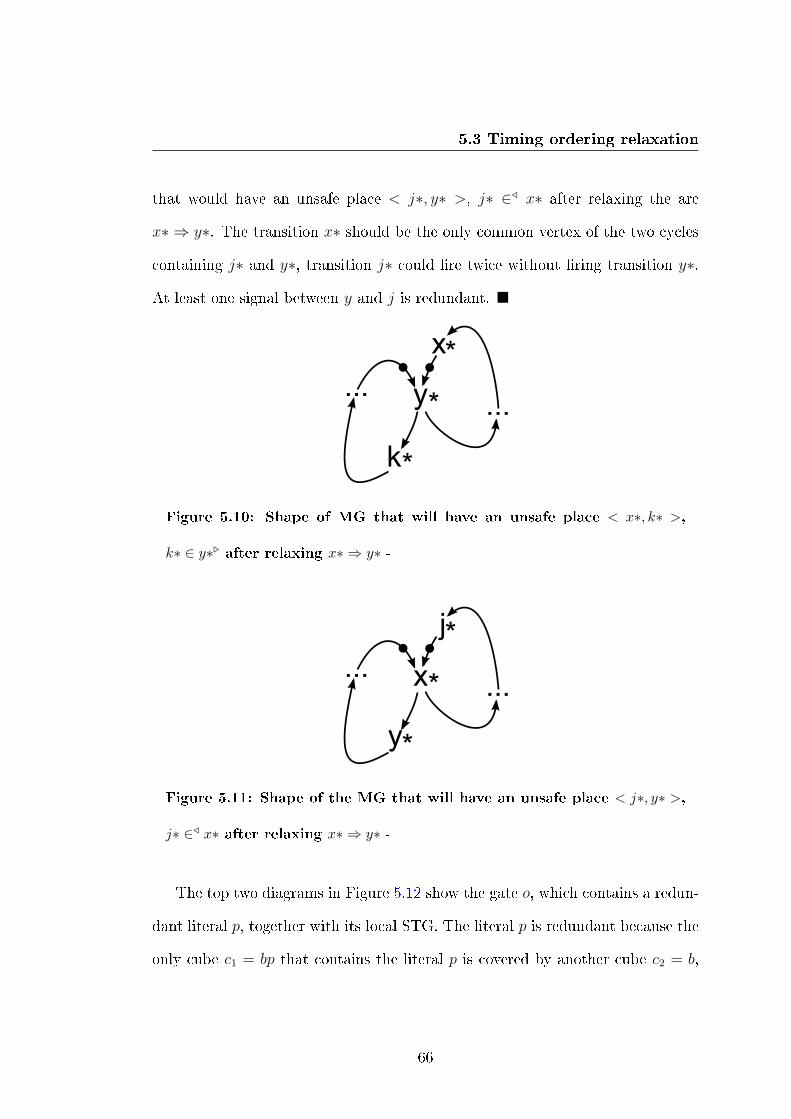
5.3 Timing ordering relaxation
that would have an unsafe place < j∗, y∗ >, j∗ ∈⊳ x∗ after relaxing the arc
x∗ ⇒ y∗. The transition x∗ should be the only common vertex of the two cycles
containing j∗ and y∗, transition j∗ could �re twice without �ring transition y∗.
At least one signal between y and j is redundant. �
x
y
k
......
*
*
*
Figure 5.10: Shape of MG that will have an unsafe place < x∗, k∗ >,
k∗ ∈ y∗⊲ after relaxing x∗ ⇒ y∗ -
x
y
j
......
*
*
*
Figure 5.11: Shape of the MG that will have an unsafe place < j∗, y∗ >,
j∗ ∈⊳ x∗ after relaxing x∗ ⇒ y∗ -
The top two diagrams in Figure 5.12 show the gate o, which contains a redun-
dant literal p, together with its local STG. The literal p is redundant because the
only cube c1 = bp that contains the literal p is covered by another cube c2 = b,
66

5.3 Timing ordering relaxation
we have c1 ⊑ c2. The literal p is redundant in gate o, the value of gate o will
never depend on the literal p. So, other input signals and the output signal of
gate o could transition more than once without waiting for any transitions on
signal p. In this situation, if we do the relaxation on arc p− ⇒ b+ on the STG,
the resulting STG will not be safe. When the redundant literal p is removed from
the gate and from its local STG, as was shown at the bottom two diagrams in
Figure 5.12, relaxation will not break the safeness on the resulting STG.
a+
p*
b+
a- b-
o-
p+
p- ab
p
o
a
bo
Remove redundant literals
a+
o+
b+
a- b-
o-
Figure 5.12: Gate o has a redundant literal p -
67

5.3 Timing ordering relaxation
5.3.3 Removing redundant arcs
The relaxation of a single arc will add a set of new arcs into the STG. Some of
the newly added arcs could be redundant. An arc is redundant 1 if the order
constraints imposed by this arc has been guaranteed by other arcs. E.g. in the
Figure 5.13, after relaxing the arcs b+ ⇒ a−, two arcs o+ ⇒ a− and b+ ⇒ o−
will be added, where the arc o+ ⇒ a− is a redundant arc. The arcs b+ ⇒ b− ⇒
o− have already constrained that b+ would happen before o−.
a+
p*
b+
a- b-
o-
a+
o+
b+
a- b-
o-
a+
o+
b+
a- b-
o-
Relax b+ a-Remove
redundant arcs
Figure 5.13: redundant arcs due to the relaxation -
Redundant arcs do not contribute to the �ow of an STG, but their existence
might complicate the relaxation and analysis processes. So, redundant arcs should
be detected and removed after new arcs are added into the STG.
1In this thesis, the term redundant is used to characterize the arcs and places which couldbe eliminated without a�ecting the �ow sequences in the underlying STG. In other literature,e.g. [61], di�erent terms (implicit place) might be used. Due to the fact, the redundancy andimplicitness is equivalent w.r.t. places in a live MG, the term redundant is used to generalizethis characteristic. The term implicit are used to characterize the un-drawn places in an MG.
68

5.3 Timing ordering relaxation
Please note that for each arc x∗ ⇒ y∗ in the local STG, there is an im-
plicit place denoted by < x∗, y∗ > on it. An arc is redundant means that the
corresponding place < x∗, y∗ > and the �ow relation w.r.t this place could be
eliminated without a�ecting the �ow sequences in the original STG. A redundant
place will never disable the �ring of one transition on its own [62]. This suggests
that the redundant place could be checked in an MG N = (P, T, F,m0) whose
marking set is M as follows,
A place p is redundant if ∀m ∈ M,m(p) = 0 ⇒ ∃p′ ∈ P∧p′ 6= p∧p′ ∈ •((p)•)∧
m(p′) = 0
However, this requires to generate the marking set of an STG and check each
marking in it. [61] suggests a method to check the redundancy of a place in an
MG structurally, which avoids the generation of marking set.
In [61], researchers had proved that in a live MG, a redundant place would
either be a loop-only place or a shortcut place.
In a live MG, a place p is a loop-only place if •p = p• ∧m0(p) = 1; a place p is
a shortcut place if there is a path σ =• p · · · p• ∧ p /∈ σ ∧∑
p′∈σ m0(p′) ≤ m0(p).
The place p4 in the Figure 5.14 (a) is a shortcut place, because there is a
path σ = (x+, p2, y+, p3, x−) between two transitions •p4 = x+ and p•4 = x− and
m0(p4) ≥∑
p′∈σ m0(p′) = m0(p2) +m0(p3) = 0.
However, the place p11 in Figure 5.14 (b) is not a shortcut place, the path
connecting two transitions •p11 = b− and p•11 = b+, which contains the least
tokens, is shown by the dotted line in the graph. The total number of tokens on
this path is two which is greater than the number of tokens in place p11.
In order to check the redundancy of a place p0, one needs to check whether
69
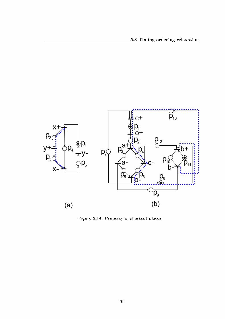
5.3 Timing ordering relaxation
(a)
x+
y+
x-
y-
p1
p2
p3
p4
p5
p1
p2p3 p4
p5 p6
p7
p8
p9
p10 p11
p12
p13c+
o+
a+
a- c-
o-
b+
b-
(b)
Figure 5.14: Property of shortcut places -
70

5.3 Timing ordering relaxation
there exists one path from •p0 to p•0 and the number of tokens on this path
should be less than or equal to the number of tokens in p0. This could be done by
changing the MG into an edge weighted directed graph and searching the shortest
path between two nodes •p0 and p•0 as was proposed in [61].
Given a marked graph MG = (T, P, F,m0), a directed graph G = (V,E)
is built by creating one node t for each transition t∗ ∈ T in MG and creating
one edge e = (•p, p•) for each place p ∈ P ∧ p 6= p0. The weight of each edge
e = (•p, p•) is the number of tokens in the place p in initial marking m0. The
edge weights in the directed graph G = (V,E) are non-negative and the shortest
path between two nodes could be solved by Dijkstra algorithm. A pseudo-code
for checking the redundancy of a place p0 in the marked graph MG is shown in
Algorithm 3. The time complexity of this algorithm is O(n2), where n is the
number of transitions in the MG.
The directed graphs corresponding to the MGs in Figure 5.14, which are used
to check the redundancy of the place p0, is shown in Figure 5.15. The dotted
arc corresponds to the place in the original MG for checking redundancy and. In
graph (a) in Figure 5.15, the shortest path from x+ to x− is x+, y+, x− whose
weight is 0, equal to the number of token in the place < x+, x− >. So, the place
< x+, x− > is redundant in the original MG. However, in graph (b), the shortest
path from b− to b+ is b−, c+, o+, a+, a−, o−, b+ whose weight is 2, larger than
the number of token in the place < b−, b+ >. So, the place < b−, b+ > is not
redundant.
71

5.3 Timing ordering relaxation
Algorithm 3 Check_place_redundancy (MG, p0)
1: V = ∅2: E = ∅3: for all transitions t∗ ∈ T in MG do4: V = V ∪ t∗5: end for6: for all places p ∈ P and p 6= p0 in MG do7: E = E ∪ (•p, p•)8: w(•p, p•) = m0(p)9: end for
10: SP = Dijkstra (V , E,w, •p0, p•0)
11: if m(p0) ≥ SP then12: return true13: else14: return false15: end if
(a)
x+
y+
x-
y-a0 b+
b-
(b)
10
0
0
1
0
0 0
0 0
0 1
0
0
0
10
0
Figure 5.15: Check for shortcut places using Dijkstra's algorithm -
72

5.4 Local STG relaxation and hazard criterion
5.4 Local STG relaxation and hazard criterion
5.4.1 Four relaxation cases
The relaxation of one arc in the STG, which will make two ordered transitions
into concurrent ones, will expand the reachable states of the STG. Whether this
relaxation is acceptable or not depends on whether the newly introduced states
cause glitches. A glitch is a premature transition, in which the output of a gate
is enabled to �re when it is expected to remain stable.
Timing conformance: A local STG of a gate o, is said to be in timing confor-
mance to gate o if in the SG of the STG: {fo↑(s) = 1|s ∈ ER(o+)∨s ∈ QR(o+)}
and {fo↓(s) = 1|s ∈ ER(o−) ∨ s ∈ QR(o−)}.
The timing conformance of a local STG with respect to a gate is that, the
output value of this gate should evaluated to "1" at each state in ER(o+) and
QR(o+) and should evaluated to "0" at each state in ER(o−) and QR(o−) in
the SG of STG.
The timing conformance of a local STG to a gate o = a · b is illustrated in
Figure 5.16, where diagram (a) and diagram (b) show the gate and its initial
local STG and the corresponding SG. Diagram (c) shows the STG, where the arc
a+ ⇒ b+ is relaxed, and the corresponding SG. In the SG of the resulting STG,
gate o evaluates to "1" in every state in ER(o+) and QR(o+) and evaluates to
"0" in every state in ER(o−) and QR(o−). So, the STG in diagram (c) is in
timing conformance to the gate o. However, the STG in diagram (d), which is
derived by relaxing the arc b− ⇒ a+ in diagram (b), is not in timing conformance
to the gate o. Because there is a state abo = 110 in QR(o−) at which the fo↑ = ab
73

5.4 Local STG relaxation and hazard criterion
a
bo
b-
a+
b+
o+
a-
o-
010
000
abo
100
110
111
011
b-
a+
b+o+
a-
o-
(a) (b)
b-
a+ b+
o+
a-
o-
010
000
abo
100
110
111
011
b-
a+
b+ o+
a-
o-
(c)
110a+
b+
b-a+
b+
o+
a-
o-
010
000
abo
100
110
111
011
b-
a+
b+o+
a-
o-
(d)
110a+
b-
Figure 5.16: Illustration of timing conformance. (a) the gate and (b)-(d)
local STGs and the corresponding SGs -
74

5.4 Local STG relaxation and hazard criterion
evaluates to "1" and the gate would prematurely �re to "1" without waiting for
the transition b+ to come.
After relaxing one arc x∗ ⇒ y∗, if the resulting STG is in timing conformance
to the gate, it indicates that the gate will be glitch-free even when the transition
x∗ comes later than transition y∗. But the reverse is NOT always true. If the
resulting STG is not in timing conformance to the gate, the gate still could be
glitch-free if the violation of timing conformance is due to unnecessary relation
constraints or the so-called "OR-causality" [63] [64].
The prerequisite transition set of the i-th occurrence of an output o∗ is de�ned
as Epre(o ∗ /i) = {z∗ : z∗ ∈ (⊳o ∗ /i)}. The output transition should only �re
when all transitions in its prerequisite transition set have �red; otherwise, the
�ring of an output transition is a glitch. The prerequisite transition set for each
transition on output signal o is calculated before relaxation and is used to check
the correctness after this relaxation has been carried out.
When an arc x∗ ⇒ y∗ belongs to the local STG of gate o, for the SG of the
resulting STG, one and only one of the following four cases will happen.
Relaxation case 1: ∀s ∈ QR(o+), fo↓(s) = FALSE and ∀s ∈ QR(o−),
fo↑(s) = FALSE.
x
yo
x+
y.
ob
x+ y.
ob
000
x+
100
y+
110
111
o+
000
x+
100
y+
110
111
o+
010
y+
x+
relax x+ -> y+
relaxation case 1
Figure 5.17: Relaxation case 1 -
75

5.4 Local STG relaxation and hazard criterion
Relaxation case 1 relates to the situation that the resulting STG is in timing
conformance to the gate. If so, the gate is guaranteed to be glitch-free under the
new STG.
Relaxation case 2: ∃s ∈ QR(o+) such that fo↓(s) = TRUE and ∀s ∈
QRi(o+) such that fo↓(s) = TRUE, s(z) = 1 if z+ ∈ Epre(o − /j); s(z) = 0
if z− ∈ Epre(o − /j), where QRi(o+) is followed by ERj(o−). Or similarly for
QR(o−), fo↑, QRi(o−) and ERj(o+).
w='0'
x
z
yo
z+ x+
y+
o+
z+x+ y+
o+
00000
00010 01000
01010 01100
01110
01111
z+ x+
x+ z+ y+
y+ z+
o+
00000
00010 01000
01010 01100
01110
01111
z+ x+
x+ z+ y+
x+ z+
o+
00100
y+
00110
x+y+
y+
z+
relax x+ -> y+
relaxation case 2.1
wxyzo wxyzo
Figure 5.18: Relaxation case 2 -
Relaxation case 2 relates to the situation that the gate evaluates to "0" ("1")
in some states in QR(o+) (QR(o−)), but in all these states, all the prerequisite
transitions have �red. Even if the resulting STG violated the timing conformance,
this situation does not indicate a glitch. This situation occurs when a transition,
which cannot be acknowledged by an output transition, is unnecessarily put into
the prerequisite set of an output transition.
The Figure 5.18 shows a gate o with its STG segment. The literal w remains at
"0" during this segment. When the arc x+ ⇒ y+ is relaxed, the transition x+ is
set to be one of the prerequisite events of o+. However, due to the gate function,
the occurrence of x+ cannot be acknowledged by o+, thus the gate becomes
76

5.4 Local STG relaxation and hazard criterion
enabled to �re o+ in state '00110' (as is indicated by the dashed square in the
�gure) in QR(o−). This is not a premature �ring, because all the transitions
{z+, y+} in the prerequisite set of o+ in the STG before relaxing have �red; the
o+ is allowed to be �red.
Relaxation case 3: ∃s ∈ QRi(o+) such that fo↓(s) = TRUE and either
x+ ∈ Epre(o − /j) and s(x) = 0 or x− ∈ Epre(o − /j) and s(x) = 1, where
QRi(o+) is followed by ERj(o−). For all s that ful�lls all conditions above, x∗
is excited in s and s′ is the state obtained by �ring x∗ in s, s′ ∈ ERj(a−). Or
similarly for QR(o−), fo↑, QRi(o−) and ERj(o+).
ox
y
x+
y+ o+
x+
y+ o+
relax x+ -> y+
100
x+
110
y+
111
000
o+
101
y+
o+
100
x+
110y+
111
000
o+
101
y+
o+
010
y+
x+
relaxation case 3
xyo xyo
Figure 5.19: Relaxation case 3 -
Relaxation case 3 applies to the situation when the gate evaluates to "0"
("1") in some states in QR(o+) (QR(o−)), and for all these states, x∗ is excited
and the states reached by �ring x∗ is in ER(o−) (ER(o+)). Relaxation case 3
is still not a hazardous situation. Because in all states in QR(o+) or QR(o−)
where the gate is ready to transit, x∗ is the only transition that belongs to the
prerequisite set of o+ or o− that has not �red yet. The reason that the gate
becomes excited without waiting for transition x∗ after relaxing the arc x∗ ⇒ y∗
is that transition y∗ could make another clause in fo↑ or fo↓ become true. This is
called OR-causality in [63] and [64]. This is not a hazard because the arc x∗ ⇒ y∗
77
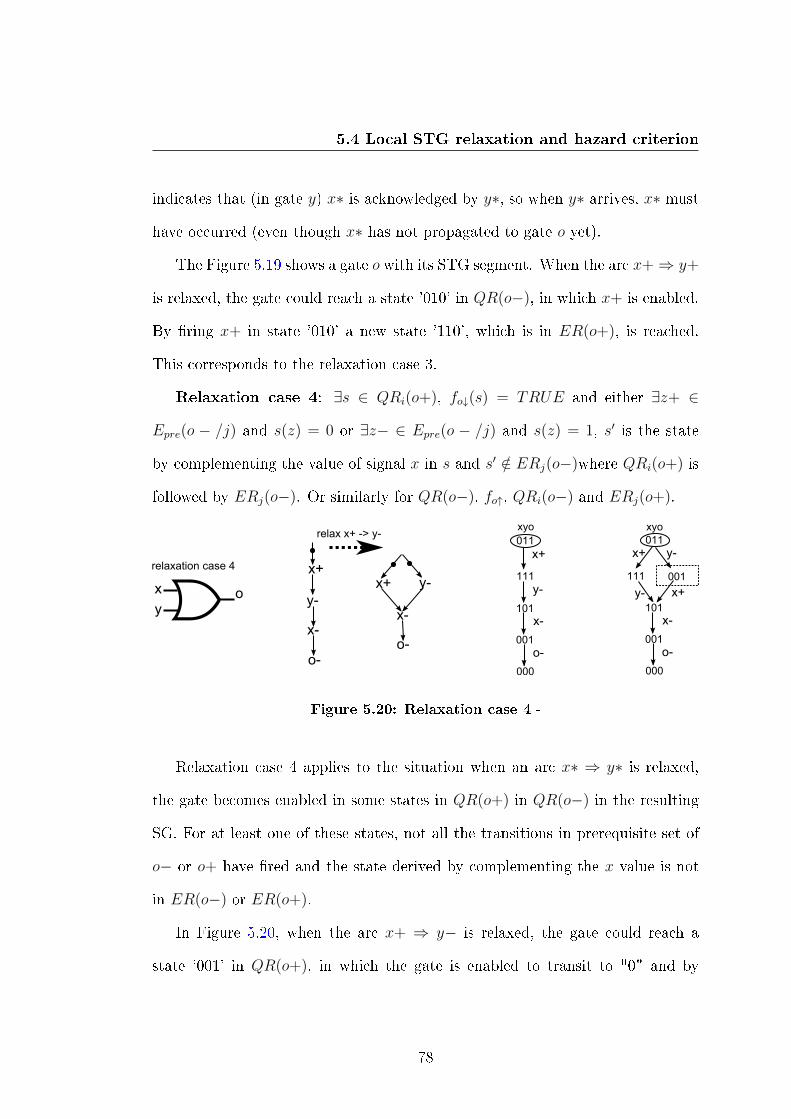
5.4 Local STG relaxation and hazard criterion
indicates that (in gate y) x∗ is acknowledged by y∗, so when y∗ arrives, x∗ must
have occurred (even though x∗ has not propagated to gate o yet).
The Figure 5.19 shows a gate o with its STG segment. When the arc x+ ⇒ y+
is relaxed, the gate could reach a state '010' in QR(o−), in which x+ is enabled.
By �ring x+ in state '010' a new state '110', which is in ER(o+), is reached.
This corresponds to the relaxation case 3.
Relaxation case 4: ∃s ∈ QRi(o+), fo↓(s) = TRUE and either ∃z+ ∈
Epre(o − /j) and s(z) = 0 or ∃z− ∈ Epre(o − /j) and s(z) = 1, s′ is the state
by complementing the value of signal x in s and s′ /∈ ERj(o−)where QRi(o+) is
followed by ERj(o−). Or similarly for QR(o−), fo↑, QRi(o−) and ERj(o+).
ox
y
x+
y-
o-
x-
x+ y-
o-
x-
relax x+ -> y-011
x+
111
y-
101
001
x-
000
o-
011
x+
111
y-101
001
x-
000
o-
001
y-
x+
relaxation case 4
xyo xyo
Figure 5.20: Relaxation case 4 -
Relaxation case 4 applies to the situation when an arc x∗ ⇒ y∗ is relaxed,
the gate becomes enabled in some states in QR(o+) in QR(o−) in the resulting
SG. For at least one of these states, not all the transitions in prerequisite set of
o− or o+ have �red and the state derived by complementing the x value is not
in ER(o−) or ER(o+).
In Figure 5.20, when the arc x+ ⇒ y− is relaxed, the gate could reach a
state '001' in QR(o+), in which the gate is enabled to transit to "0" and by
78

5.4 Local STG relaxation and hazard criterion
complementing the value of x in state '001', the newly reach state '101' is still in
QR(o+). The relaxation case 4 is equal to that in the "problematic" state, there
exists another transition in the prerequisite set of o+ or o− other than x∗, which
has not �red yet.
The relaxation case 1 indicates the relaxation of arc x∗ ⇒ y∗ will be accepted
immediately. The STG will be updated for further operation. The relaxation
case 4 indicates the relaxation will be rejected and one timing constraint x∗ ≺ y∗
(which means that x∗ must reach the gate before y∗) will be generated to prevent
the gate from entering the hazardous states. The relaxation cases 2 and 3 requires
further modi�cations of the STG.
The relaxation case 2 happens when a transition x∗, which is not necessary for
the �ring of the output transition o∗, is relaxed into one of prerequisite transitions
of o∗. The gate o could become enabled without waiting for the occurrence of x∗,
so the gate becomes excited in some states in QR(o∗). In this case, x∗ should be
concurrent with o∗, which is done by relaxing the arc x∗ ⇒ o∗. There could be
two cases after making x∗ to be concurrent with o∗.
The �rst case is exempli�ed in Figure 5.21 (a), where after making x+ to
be concurrent with o+, fo↑ is true in every state in ER(o+). However, in the
second case, there exists one state s ∈ ER(o+) such that fo↑ is false in s. One
example for the second case is shown in Figure 5.21 (b), x+ is not necessary for
o+, because there is another transition z+ which is concurrent with o+ and if z+
reaches gate o earlier than x+, it will trigger o+ instead of x+. This means that
neither z+ nor x+ is necessary for o+, neither of them could be a prerequisite
transition of o+. So, when x+ is relaxed to be one of prerequisite transition of
79
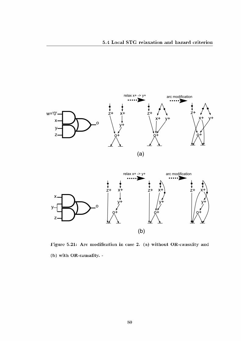
5.4 Local STG relaxation and hazard criterion
w='0'
x
z
yo
z+
x+
y+
o+
z+x+ y+
o+
relax x+ -> y+
z+x+ y+
o+
arc modification
x
z
y o
z+
y+
o+
x+z+
y+
o+
relax x+ -> y+
x+
arc modification
x+z+
y+
o+
(a)
(b)
Figure 5.21: Arc modi�cation in case 2. (a) without OR-causality and
(b) with OR-causality. -
80

5.5 Optimal relaxation order
o+, it must be made to be concurrent with o+ as discussed above. However,
when x+ is modi�ed to be concurrent with o+, the ER(o+) could be entered by
just �ring y+ in the initial marking, where fo↑ is still false. This happens because
the enabling of gate o needs at least one transition between x+ and z+ to happen
�rst, but neither of them are necessary for o+, when both of them are concurrent
with o+, the ER(o+) could be entered when fo↑ is still false. This problem is
caused by the OR-causality, where the enabling of a gate could be caused by more
than one option. Both relaxation case 2 and case 3 could meet the OR-causality.
The details of OR-causality situation and decomposition of the OR-causality will
be speci�ed in detail in Chapter 6.
5.5 Optimal relaxation order
Di�erent relative timing constraint sets might be derived if arcs are relaxed in
di�erent orders. This is because there might be more than one way to prevent a
gate entering a hazardous state.
The diagram (a) in Figure 5.22 show an STG segment whose SG (shown in
diagram (b)) contains a hazardous state s. There are two approaches to forbid
the circuit to visit this hazardous state (timing constraints are denoted by &):
1) to force c+ before a+ (the corresponding STG segment and SG are shown in
diagram (c) and (d)); 2) to force b+ to come before a+ (the corresponding STG
segment and SG are shown in diagram (e) and (f)).
One example which shows di�erent timing constraints due to di�erent relax-
ation orderings is presented in Figure 5.23. Four di�erent sets of timing con-
81

5.5 Optimal relaxation order
a+
b+
ca
baba
baa+
ca
caca
a+
a+
constraint 1
s
b+c+
b+ b+
a+
c+
a+
constr
aint 2
constraint 1 : c+ < a+
b+c+
b+
c+c+a+
a+constraint 2 : b+ < a+
a+
c+ b+
a+
c+ b+
a+
c+ b+
& &
(a) (c) (e)
(b) (d) (f)
Figure 5.22: Preventing the gate entering hazardous state s -
straints could guarantee the correctness of the circuit:
1) {x+ ≺ y−, y+ ≺ z+} (relax x+ ⇒ z+ before y+ ⇒ z+ and then relax
y+ ⇒ x− before x+ ⇒ y−);
2) {y+ ≺ x−, y+ ≺ z+}(relax x+ ⇒ z+ before y+ ⇒ z+ and then relax
x+ ⇒ y− before y+ ⇒ x−);
3) {x+ ≺ z+, y+ ≺ x−} (relax y+ ⇒ z+ before x+ ⇒ z+ and then relax
x+ ⇒ y− before y+ ⇒ x−) and
4) {x+ ≺ z+, x+ ≺ y−} (relax y+ ⇒ z+ before x+ ⇒ z+ and then relax
y+ ⇒ x− before x+ ⇒ y−).
We prefer to generate the optimal one during the relaxation process rather
than generate all of the cases and choose the best one. Exhaustion of all relaxation
orders implies a time complexity of O(n! ), where n is the number of arcs to be
82

5.5 Optimal relaxation order
relaxed, and most of these relaxations lead to the same results.
xyz
o
y-
o-
x+ y+
z+
x- y-
o+
z-
o-
x+ y+
z+
x- y-
o+
&
&
z-
o-
x+ y+
z+
x- y-
o+
&
&
z-
o-
x+ y+
z+
x- y-
o+
&
&
z-
o-
x+ y+
z+
x- y-
o+
&
&
Expand
1) 2) 3) 4)
Figure 5.23: Di�erent timing constraints due to di�erent relaxation or-
dering -
The weakest constraint set could be generated by relaxing the tightest arc at
each step. This will relax tighter arcs as much as possible before they become
the necessary timing requirement to avoid entering the hazardous state. In Fig-
ure 5.24, when deciding which of the two arcs c+ ⇒ a+ and b+ ⇒ a+ should be
relaxed �rst, their weights (the level of adversary path) could be calculated from
the STGimp. The STGimp explicitly presents adversary paths; for example, viola-
tion of the arc c+ ⇒ a+ needs two adversary paths c+ ⇒ p− ⇒ q+ ⇒ h− ⇒ a+
and c+ ⇒ m− ⇒ n+ ⇒ a+ to be faster than the wire between fan-out of gate
c and fan-in of gate a. If all the signals p, q, h,m, n, k, l are internal signals, the
weight of arc c+ ⇒ a+ is three and that of arc b+ ⇒ a+ is two. The arc
b+ ⇒ a+ is tighter than arc c+ ⇒ a+ and should be relaxed �rst. If there are
several arcs of the same tightness, one arc will be picked randomly. The function
find_tightest_arc(STG) returns the tightest input to input arc in a local STG
of a gate, whose ordering has not been guaranteed yet.
83

5.6 Top level algorithm
a+
cb b+
a+
cb b+
p-
q+
m-
n+
h-
k-
l+
local STG whole STG
Figure 5.24: Calculate the weight of an arc from STGimp -
5.6 Top level algorithm
The top level algorithm of the proposed method is shown in Algorithm 5, where
the input STG will be decomposed into a set of MGs by the function Decom-
pose_into_MG(STG) using Hack's algorithm [8] if it contains free-choice places.
Then the local STG for each internal (denoted by R) and primary output (de-
noted by O) signal a will be generated by the function Proj(MG, a∪ fan-in(a))
introduced in Algorithm 1. The timing constraints for a gate a to work correctly
under an MG component will be derived in Algorithm 4 using the processes an-
alyzed in the previous sections. The function Write_sg(STG) generates the SG
of an STG using the method presented in [48]. Function Relax(STG, x∗ ⇒ y∗)
is the arc relaxation algorithm de�ned in Algorithm 2. Function Check(SG, fa↑,
fa↓) decides which relaxation case will be due to the criteria introduced in this
chapter. Lines 10-14 and 20-24 depict the OR-causality decomposition in relax-
ation case 2 and 3, which will be speci�ed in detail in the next chapter. The
84

5.6 Top level algorithm
timing constraint the transition x∗ should arrive at gate a before y∗ is denoted
as a : x∗ ≺ y∗ in line 28. The timing constraints for a circuit to work correctly
when the isochronic fork is relaxed is the union of the timing constraints of all
gates under all MG components.
5.6.1 Complexity analysis
The time complexity of decomposing a free-choice STG into MGs using Hack's
algorithm grows exponentially with respect to the number of choice places in an
STG. However, the number of choice places in an STG is decided by the function
of the circuit not the scale of the circuit. Usually, an STG does not contain a
large number of choice places.
The complexity for deriving the local STGs for all gates in an SI circuit is
O(n6) with respect to the number of transitions (n) in the STG. In the worst case,
there are O(n) gates which need deriving their local STGs. There are up to O(n)
transitions needing to be eliminated for each local STG. When one transition is
eliminated, each arc in the resulting STG needs to be checked for redundancy.
The complexity for checking the redundancy of one arc is O(n2) and a graph
which has O(n) transitions could have up to O(n2) arcs.
When an STG is decomposed into a set of local STGs, checking hazards for
all gates is performed on their local STGs. Thus, the complexity for the hazard
checking work increases linearly with respect to the number of gates in the circuit.
So, the complexity of the proposed technique increases exponentially as the
number of choice places in an STG. When the number of choice places in the
85

5.6 Top level algorithm
STG is considered to be a constant, the asymptotic computation complexity is
O(n6), where n is the number of transitions in the STG.
Algorithm 4 Expand (STGa, fa↑, fa↓, Rt)
1: while STGa contains input to input arcs whose ordering is not guaranteed do
2: x∗ ⇒ y∗ = �nd_tightest_arc (STGa)3: new_STGa = Relax (STGa, x∗ ⇒ y∗)4: if Check (Write_sg (new_STGa), fa↑, fa↓) == relaxation case 1 then
5: STGa = new_STGa
6: else if Check (Write_sg (new_STGa), fa↑, fa↓) == relaxation case 2 then
7: if Check (Write_sg (Relax (new_STGa, x∗ ⇒ a∗), fa↑, fa↓) == relaxation case 1 then
8: STGa = Relax (new_STGa, x∗ ⇒ a∗)9: else
10: STGa = new_STGa
11: Cans_set = �nd_candidate_transitions (STGa)12: Init_cons = �nd_initial_restrictions (STGa)13: Solution_group = OR_causality_decomposition (Cans_set, Init_cons)14: SubSTGsa = Add_restriction_arcs_case2 (STGa, Solution_group)15: for all STGa' ∈ SubSTGsa do
16: Expand (STGa', fa↑, fa↓, Rt)17: end for
18: end if
19: else if Check (Write_sg (new_STGa), fa↑, fa↓) == relaxation case 3 then
20: STGa = new_STGa
21: Cans_set = �nd_candidate_transitions (STGa)22: Init_cons = �nd_initial_restrictions (STGa)23: Solution_group = OR_causality_decomposition (Cans_set, Init_cons)24: SubSTGsa = Add_restriction_arcs_case3 (STGa, Solution_group)25: for all STGa' ∈ SubSTGsa do
26: Expand (STGa', fa↑, fa↓, Rt)27: end for
28: else
29: Rt = Rt ∪ {a : x∗ ≺ y∗}30: Mark the arc {x∗ ⇒ y∗} has been guaranteed yet31: end if
32: end while
5.6.2 Proof of correctness
The starting point of the proposed method is an SI circuit and an STG describing
its behavior. The SI circuit conforms to the STG, which means that the circuit is
functionally correct and hazard-free. The relaxation operation only relaxes arcs
between two transitions on the input signals of a gate, which is equivalent to
changing two ordered input transitions into concurrent. This modi�cation does
86

5.6 Top level algorithm
Algorithm 5 Deriving_timing_constraints( STGimp, C)
1: Rt = ∅2: MG = Decompose_into_MG(STGimp)3: for all MGi ∈ MG do4: for all signal a ∈ R ∪O do5: STGa = Proj(MGi, a ∪ fan− in(a))6: Expand (STGa, fa↑, fa↓, Rt)7: end for8: end for9: return Rt
not change the interface protocol between a gate and its environment and thus
could only introduce hazards but will not harm the functionality of the gate.
Interface protocol will only be changed if the OR-causality relation happens,
where the corresponding transition on output signal will be triggered by a di�erent
clause of the gate. However, this is a local e�ect, that the environment could only
receive the output transition when it has sent the input transitions required by
the gate in the initial STG. As will be analyzed in the next chapter, the subSTGs
generated by the proposed OR-causality decomposition method cover all possible
�ring sequences when an OR-causality occurs. The relaxation operation will keep
the liveness and consistency of the STG nor will the safeness be violated if the
gate does not contain redundant literals. These three properties guarantee that
when an arc in the STG is relaxed the resulting STG is still a valid representation
of the behavior of the gate. Each time when an arc is relaxed, this relaxation will
be accepted if it does not introduce hazards; or will be rejected if it does.
In section 5.3.2 we have proved that the relaxation operation does not destroy
the liveness and consistency of the STG. Also, the safeness will not be a�ected if
the circuit does not have redundant literals. This suggests that the whole process
87

5.7 Delay padding to ful�ll timing constraints
will eventually terminate. Indeed, when an arc is relaxed, more states could be
reached by the resulting STG (if the relaxed arc is not a redundant one). For
a live and safe STG with n signals, there are at most 2n reachable states. The
whole process will eventually converge.
5.7 Delay padding to ful�ll timing constraints
When the relaxation is done, all of the generated timing constraints could be
changed into the pairwise delay constraints between a wire and a path by track-
ing back to the STGimp and looking up the Circuit C. The circuit will work
correctly if these constraints are guaranteed. Some constraints could be consid-
ered to be "safe" (e.g. adversary path cross environment or a very long adversary
path), some constraints could be guaranteed by layout. If there are very strong
constraints (very short adversary path) and the technology variations are severe,
all these strong constraints could be guaranteed by delay padding.
The padding technique will not be investigated in detail, because the number
of strong constraints in an SI is usually not large. Therefore, �nding a good
padding positions in a circuit is not a di�cult task when the timing constraints
have been generated. A simple heuristic that could �nd a good padding positions
in most cases is introduced below.
There are two kinds of padding positions: padding on a wire and padding
on a gate. Figure 5.25 shows the possible padding positions (position 1-5) to
guarantee the delay constraint that a wire from gate g_1 to g_4 should be
faster than another path between these two gates. Padding on position 1, 3 or 5
88

5.7 Delay padding to ful�ll timing constraints
(padding on wire), only delays transitions on one branch of a gate; while padding
on position 2 or 4 (padding on gate) will delay all branches of a gate output, which
is equivalent to the increase of the delay of a gate. Padding on a gate could always
ful�ll one delay constraint without worsening other delay constraints, but might
unnecessarily delay other branches in a fork; while padding on a wire has less
performance penalty but may degrade another delay constraint if the wire that
the delay padded on should be faster than another adversary path. A greedy
padding policy could be used which tries to pad the delay on position 1 if the
corresponding wire does not participate in another delay constraint. If it does,
then the greedy algorithm tries to pad on position 3. In the worst case when all
the wires in the adversary path are in some other delay constraints then pad on
the position 2 could break this cyclic dependency.
...
...
......
...
...
12
34
5g_1
g_2 g_3
g_4
Figure 5.25: Padding positions -
Due to the padding rule described above it could be guaranteed that all of
the delay constraints could be ful�lled (padding on the last gate could always
ful�ll this delay constraint without worsening another path, like the technique
used in synthesis in [9]). Usually, a good padding method to get the minimum
performance penalty is to try to pad delays on the wire near the destination gate
of an adversary path such that this wire is not in the fast path of another delay
89
5.8 Summary
constraint by looking up the delay constraint table(as was exempli�ed in Table
7.1 in Chapter 7).
5.8 Summary
This chapter introduces our method to generate a set of timing constraints for
an SI circuit to work correctly when the isochronic fork timing assumption is re-
laxed into the intra-operator timing assumption. The method generates the local
environments for all gates in the circuit and operates on these local environments
to avoid exploring the reachability space of the entire circuit. In each local en-
vironment, the timing constraints implied by the isochronic fork will be relaxed
one by one. Unnecessary timing constraints will be removed in the relaxation
process. The computational complexity of the proposed method is polynomial to
the number of signals in the circuit and the generated timing constraints could
always be ful�lled.
90

Chapter 6
OR-causality Decomposition
The relaxation case 2 and case 3 presented in the chapter 5 do not imply a glitch at
a gate. They violate the timing conformance because the so-called OR-causality
happens. This chapter analyzes the situation in which an OR-causality relation
would appear in the local STG in relaxation case 2 and case 3 and proposes a
method to decompose the STG into a set of subSTGs. The subSTGs are then
treated as individual STGs and are processed one by one iteratively. A gate will
work properly if it works properly in every subSTG.
6.1 OR-causality
The �ow semantics of PNs, an event is enabled if and only if all of its input places
have tokens, explicitly expresses the strong causality (AND-causality) between
events. It is easy to describe the causality like this: events a and b must occur
before the event c. However, the weak causality (OR-causality) like: event c is
91

6.1 OR-causality
enabled if any event of a and b occurs, is not easy to be represented in PNs. This
kind of causality might appear in the local STG during the relaxation process.
When two ordered transitions in the local STG are made to be concurrent by
the relaxation operation, more than one clause could evaluate from false to true
concurrently. The corresponding pull up/down function would become true and
cause the gate to transit when any of its clause evaluates true. OR-causality
relations between clauses cannot be expressed by a safe or free-choice PN. In
order to describe the behavior of a gate using safe MGs where the proposed
relaxation method could work, the local STG needs to be decomposed into a set
of subSTGs when the OR-causality relations between transitions are encountered.
The OR-causality in relaxation case 2 and case 3 will be analyzed in detail in this
section and the decomposition method will be introduced in the next section.
6.1.1 OR-causality in relaxation case 2
OR-causality in relaxation case 2: Relaxation case 2 happens if and only if
there is a transition y∗ which is a prerequisite transition of o∗ and the relaxation
of an arc x∗ ⇒ y∗ makes x∗ to be a prerequisite transition of o∗, but o∗ could
also be caused by other transitions if x∗ is delayed. Due to the relaxation rule, x∗
must then be made concurrent with o∗ because the transitions in the prerequisite
set of o∗ are those that must be necessary for the �ring of o∗. However, if the
clause containing x∗ is the last clause whose literals are all ordered with o∗ then
making x∗ concurrent with o∗ will cause fo↑ to become false in some states in
ER(o+) or fo↓ to become false in some states in ER(o−).
92

6.1 OR-causality
The Figure 6.1 shows an example that contains OR-causality in relaxation
case 2. The pull up function fo↑ of the gate o has three clauses, x · y, z · k · y and
m · y · n. Initially, when the arc k+ ⇒ y+ in the STG in diagram (b) is relaxed,
k+ is placed to be a prerequisite transition of o+ as is shown in diagram (c).
Apparently, fo↑ could also become true if clause x ·y or m ·n ·y becomes true. So,
k+ needs to be modi�ed to be concurrent with o+ by relaxing the arc k+ ⇒ o+.
The resulting STG shown in diagram (d) will be accepted because all the literals
in clause x · y are still ordered with o+ which guarantees that fo↑ is true in each
state in ER(o+). However, when the arc x+ ⇒ y+ in the STG in diagram (d)
is relaxed, x+ should also be modi�ed to be concurrent with o+. After that, the
STG in diagram (f) could enter ER(o+) after m+ and y+ �res but the pull up
function of the gate o, fo↑, is still false.
The reason for this is that in the STG segment, any of the three clauses x · y,
z·k·y andm·y·n could cause fo↑ to become true, thus only the transition y+, which
corresponds to their common literal y, is necessary for o+. All other transitions
cannot be placed at the prerequisite transitions of o+. But it is required that
all literals in at least one clause are ordered with o+ to guarantee that when the
STG enters the ER(o+) this clause could enable gate o to transit to high. When
any literal (x+ in this example) of the last clause that are ordered with o+ (the
clause x · y in this example) is modi�ed to be concurrent with o+, the STG could
enter ER(o+) without any clause becoming true.
When more than one clause could become true simultaneously and enable the
gate to transit, a safe MG cannot describe this race behavior. In order to describe
the behavior of a gate under OR-causality using MGs, the original local STG
93

6.1 OR-causality
x
zy o
relax x+ -> y+ arc modification
relax x+ -> o+
mn
k
x+
y+
relax k+ -> y+
arc modification
relax k+ -> o+
m+
o+
z+ n+k+x+
y+
m+
o+
z+ n+k+
x+
y+
m+
o+
n+k+z+x+
y+
m+
o+
n+k+z+
x+
y+
m+
o+
n+k+z+
(a) (b) (c)
(d) (e) (f)
Figure 6.1: OR-causality in relaxation case 2. (a) the gate and (b)-
(f)relaxation steps -
94

6.1 OR-causality
needs to be decomposed into a set of subSTGs. The OR-causality decomposition
is done by adding concurrency restriction arcs between the transitions involved
in the OR-causality relation, to guarantee that for each subSTG, one clause will
always evaluate true before (or not later than if clauses have common literals) all
other clauses, the transition on output signal is then unambiguously caused by
that clause.
Candidate clauses are the clauses which have a possibility to win the race
to cause the transition on the output signal. The candidate clauses for the OR-
causality in relaxation case 2 could be derived by testing whether one clause could
�rstly evaluate true among all clauses in the "problematic" states.
Candidate clause for OR-causality in relaxation case 2 : In relaxation
case 2, when the OR-causality happens, a clause c in fo↑ (if fo↑ is false in some
states in ER(o+)) is called a candidate clause if,
(1) In the SG corresponding to the STG before arc modi�cation, there exist
two states s and s′ in QR(o−), s → s′, fo↑(s) = false, fo↑(s′) = true and clause
c is true in s′.
Or,
(2) Clause c contains all prerequisite transitions of o∗.
A clause c in fo↓ (if fo↓ is false in some states in ER(o−)) is called a candidate
clause if,
(1) In the SG corresponding to the STG before arc modi�cation, there exist
two states s and s′ ∈ QR(o+), s → s′, fo↓(s) = false, fo↓(s′) = true and clause
c is true in s′;
Or,
95

6.1 OR-causality
(2) Clause c contains all prerequisite transitions of o∗.
Not all transitions, which correspond to literals in a candidate clause, will
be used for the OR-causality decomposition. Some transitions are guaranteed
to occur before the OR-causality relation happens by the arcs in the current
STG. The decomposition only involves those transitions whose occurrences could
in�uence the order of clause evaluation.
Candidate transition for OR-causality decomposition: A transition t∗
is called a candidate transition for the OR-causality decomposition if,
(1) there is a candidate clause c, t ∈ c if t∗ is t+, t̄ ∈ c if t∗ is t− and t∗ is
concurrent with o∗.
(2) t∗ is x∗, if this OR-causality is caused by relaxing x∗ ⇒ y∗.
A candidate clause is a clause which could make fo↑ from false to true in
QR(o−) or fo↓ from false to true in QR(o+) when the OR-causality happens.
Candidate transitions are those transitions whose literals appear at a candidate
clause and are concurrent with o∗ or this transition is x∗.
x
zy o
mn
k
x+
y+
m+
o+
n+k+z+
x+
y+
m+
o+
n+
k+
z+
(a) (b) (c)
Figure 6.2: Candidate clause and transition for OR-causality in relax-
ation case 2. (a) the gate, (b) and (c) two di�erent STG segments -
96

6.1 OR-causality
Figure 6.2 shows a gate o in diagram (a) together with two di�erent STG
segments in diagrams (b) and (c). In both STG segments, relaxation case 2
happens after relaxing x+ ⇒ y+ and after modifying the x+ to be concurrent
with o+, OR-causality happens. There are three candidate clauses z ·k ·y, m ·n ·y
and x·y in the STG segment in diagram (b), but only two candidate clauses z ·k ·y
and x ·y in the STG segment in diagram (c). In diagram (b), when the transitions
m+, y+, z+ and k+ �re the fo↑ turns from false to true; when the transitions
m+, y+ and n+ �re the fo↑ turns from false to true. However, in diagram (c),
there are no �ring sequences by which the clause m · n · y could make fo↑ turn
from false to true, because when the clause m · n · y becomes true the clause
z · k · y has already become true. The candidate transitions in diagram (b) are
z+, k+ for the candidate clause z · k · y (y+ is not concurrent with o+), n+ for
the candidate clause m ·n ·y (m+ and y+ are not concurrent with o+) and x+ for
the candidate clause x · y. The candidate transitions in diagram (c) are z+, k+
for the candidate clause z · k · y and x+ for the candidate clause x · y.
6.1.2 OR-causality in relaxation case 3
OR-causality in relaxation case 3: Relaxation case 3 happens if and only if
x∗ is a prerequisite transition of o∗ and the relaxation of an arc x∗ ⇒ y∗, which
makes y∗ to be concurrent with x∗, causes at least one clause containing the
literal y but not containing the literal x in fo↑ to become true in QR(o−) or in
fo↓ to become true in QR(o+).
The Figure 6.3 shows an example that contains OR-causality in relaxation
97
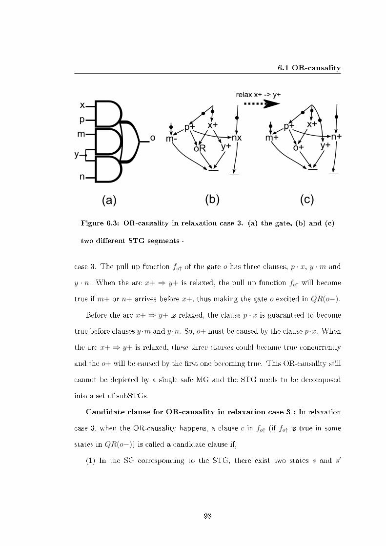
6.1 OR-causality
x
y
om
n
x+
y+oR
m- nx
p
relax x+ -> y+
p+ x+
y+o+m+ n+
p+
(a) (b) (c)
Figure 6.3: OR-causality in relaxation case 3. (a) the gate, (b) and (c)
two di�erent STG segments -
case 3. The pull up function fo↑ of the gate o has three clauses, p · x, y ·m and
y · n. When the arc x+ ⇒ y+ is relaxed, the pull up function fo↑ will become
true if m+ or n+ arrives before x+, thus making the gate o excited in QR(o−).
Before the arc x+ ⇒ y+ is relaxed, the clause p · x is guaranteed to become
true before clauses y ·m and y ·n. So, o+ must be caused by the clause p·x. When
the arc x+ ⇒ y+ is relaxed, these three clauses could become true concurrently
and the o+ will be caused by the �rst one becoming true. This OR-causality still
cannot be depicted by a single safe MG and the STG needs to be decomposed
into a set of subSTGs.
Candidate clause for OR-causality in relaxation case 3 : In relaxation
case 3, when the OR-causality happens, a clause c in fo↑ (if fo↑ is true in some
states in QR(o−)) is called a candidate clause if,
(1) In the SG corresponding to the STG, there exist two states s and s′
98

6.1 OR-causality
∈ QR(o−), s → s′, fo↑(s) = false, fo↑(s′) = true and clause c is true in s′.
Or,
(2) The clause c is the clause that contains all prerequisite transitions of o∗.
A clause c in fo↓ (if fo↓ is true in some states in QR(o+)) is called a candidate
clause if,
(1) In the SG corresponding to the STG, there exist two states s and s′
∈ QR(o+), s → s′, fo↓(s) = false, fo↓(s′) = true and clause c is true in s′.
Or,
(2) The clause c is the clause that contains all prerequisite transitions of o∗.
Candidate transition for OR-causality decomposition: A transition t∗
is called a candidate transition for OR-causality decomposition if,
(1) there is a candidate clause c, t ∈ c if t∗ is t+, t̄ ∈ c if t∗ is t− and t∗ is
concurrent with o∗.
(2) t∗ is x∗, if this OR-causality is caused by relaxing x∗ ⇒ y∗.
Figure 6.4 shows a gate o in diagram (a) together with two di�erent STG
segments in diagrams (b) and (c). In both STG segments, OR-causality happens.
There are three candidate clauses y · m, y · n and p · x in the STG segment in
diagram (b), but only two candidate clauses y · n and p · x in the STG segment
in diagram (c). In diagram (b), when the transitions p+, m+ and y+ �re the
fo↑ turns from false to true; when the transitions p+, n+ and y+ �re the fo↑
turns from false to true. However, in diagram (c), there are no �ring sequences
by which the clause yn could make fo↑ turn from false to true, because when the
clause y ·n becomes true the clause y ·m has already become true. The candidate
transitions in diagram (b) are m+, y+ for the candidate clause y ·m, n+, y+ for
99

6.2 Decomposition of OR-causality
the candidate clause y · n and x+ for the candidate clause p · x. The candidate
transitions in diagram (c) are m+, y+ for the candidate clause y ·m and x+ for
the candidate clause p · x.
Both OR-causality relations between clauses in relaxation cases 2 and 3 need
the STG to be decomposed into a set of subSTGs, and the technique that achieves
this will be introduced in the next section.
x
y
om
n
px+
y+o+m+ n+
p+ x+
y+o+m+ n+
p+
(a) (b) (c)
Figure 6.4: Candidate clause and transition for OR-causality in relax-
ation case 3. (a) the gate, (b) and (c) two di�erent STG segments -
6.2 Decomposition of OR-causality
OR-causality during the relaxation is the situation when the isochronic fork tim-
ing assumption is relaxed, more than one clause in a pull-up or pull-down function
of a gate could (depending on which of them become true �rst) cause a transi-
tion at the gate's output. This race relation cannot be depicted by a safe MG.
In order to describe the behavior of a gate using MG, the corresponding local
STG needs to be decomposed into a set of subSTGs where each subSTG does not
100

6.2 Decomposition of OR-causality
contain OR-causality relations and the union of reachable states of all subSTGs
should contain all the states that could be reached by the original STG when
OR-causality happens.
The diagrams (a) and (b) in Figure 6.5 show a gate o and its local STG
segment that were introduced before in Figure 6.2. The STG segment in diagram
(b) contains OR-causality relations where any of the three clauses x · y, z · k · y
and m ·n ·y could trigger a rising transition at the gate o output when it becomes
true and there are no constraints on which of these three clauses will become
true �rst. Diagrams (c) to (g) are the decomposed subSTG segments of the
STG segment in diagram (b). In each subSTG, the OR-causality relation is
eliminated by adding order-restriction arcs (arcs marked with a '#' symbol ).
The order-restriction arcs are added between candidate transitions in an OR-
causality, which restrict the orderings of candidate transitions in di�erent clauses
to guarantee that one candidate clause will always become true before all others,
the output transition is then clari�ed to be caused by that clause. For example,
the diagrams (c) and (d) depict the subSTGs where the output transition o+ is
caused by the clause x · y, diagram (e) depicts the subSTG where o+ is caused
by clause z ·k ·y and diagram (f) and (g) depict the subSTGs where o+ is caused
by clause m · n · y. The OR-causality decomposition only restricts the ordering
between the candidate transitions, so, the transition m+ in the diagram will
not be considered in the decomposition but it will be considered when the arc
m+ ⇒ y+ is relaxed and the corresponding STG entering OR-causality again in
the following subSTG relaxation. The union of the states reached by diagram (c)
to (g) includes all the states that the gate o could exhibit in diagram (b).
101

6.2 Decomposition of OR-causality
x
zy o
mn
k
x+
y+
m+
o+
n+k+z+x+
y+
m+
o+
n+k+z+ ## x+
y+
m+
o+
n+k+z+ ##
x+
y+
m+
o+
n+k+z+ #x+
y+
m+
o+
n+k+z+ ### #
#
x+
y+
m+
o+
n+k+z+ #
#
OR-causality
decomposition
(a)
(b) (c)
(e)
(d)
(f) (g)
Figure 6.5: OR-causality decomposition example. (a) the gate, (b) STG
segment before decomposition and (c)-(g)resulting subSTG segments -
102

6.2 Decomposition of OR-causality
An order-restriction arc behaves like a normal arc in PN semantics except
that it will not be relaxed (the ordering of the two events connected by a order-
restriction arc is considered to be �xed) and it will not be checked for redun-
dancy, which means even if an order-restriction arc is redundant it will not be
eliminated. The elimination of an order-restriction arc might cause STG enter-
ing OR-causality relation again in the future relaxation and cause the additional
unnecessary OR-causality decomposition. Keep the redundant order-restriction
arcs in an STG will not cause any trouble, because they will not be relaxed any
more.
The technique to decompose an STG which contains an OR-causality will be
demonstrated on a set of examples, from simple to complex.
The decomposition of an STG containing OR-causality is a technique to add
order-restriction arcs to concurrent candidate transitions between di�erent clauses
to make sure that one clause will become true before other clauses. The subSTGs
should include all the states that could be reached by the gate under this OR-
causality and the decomposition that contains fewer subSTGs is preferred (each
subSTG needs to be analyzed one by one, fewer subSTGs implies less computa-
tion).
A set of concurrency restriction arcs are generated for each subSTG during
the OR-causality decomposition. The subSTG is then derived by adding these
arcs into the original STG and modifying some causalities when needed. For
example, the set of concurrency restriction arcs for the subSTG in diagram (c) in
Figure 6.5 are {x+ ≺ k+; x+ ≺ n+}. The solution of an OR-causality decompo-
sition is a group of sets of concurrency restriction arcs, one set for each subSTG.
103

6.2 Decomposition of OR-causality
The solution for the OR-causality in Figure 6.5 is:
S =
Sx =
{
{x+ ≺ k+; x+ ≺ n+}{x+ ≺ z+; x+ ≺ n+}
Szk ={
{z+ ≺ x+; k+ ≺ x+; z+ ≺ n+; k+ ≺ n+}
Sn =
{
{n+ ≺ x+;n+ ≺ k+}{n+ ≺ x+;n+ ≺ z+}
Firstly, consider the simplest situation, where an OR-causality relation only
involves two clauses ca and cb. The clause ca will become true when all the
candidate transitions in set A �re and the clause cb will become true when all
transitions in set B �re. The task is to generate a set of subSTGs such that
in each subSTG the clause ca evaluates true before the clause cb, and the set of
states in the SGs of all subSTGs includes all the states in which the clause ca will
evaluate true before the clause cb.
For example, suppose the clause ca becomes true when all the candidate tran-
sitions in set A = {a+, b+, c+} �re and clause cb becomes true when all the can-
didate transitions in set B = {d+, e+, f+} �re. Initially, there are no constraints
about the �ring order relation among these transitions. There are P 66 = 720
di�erent �ring sequences. When a restriction a+ ≺ d+ is added, it excludes all
�ring sequences that d+ �res before a+. The question is how to �nd a group
of restriction sets such that in each constraint set, there are only pairwise order
constraints between two transitions (like a+ ≺ d+). The order constraints in
a constraint set work together to limit the �ring sequences this constraint set
expresses. The union of the �ring sequences of all constraint sets contains all
sequences in which all transitions in set A �re before at least one transition in set
B and contains no sequences in which all transitions in set B �re before at least
104

6.2 Decomposition of OR-causality
one transition in set A. Among all of the groups which ful�ll the requirement
above, the one which contains the fewest number of sets is preferred.
For example, in the group
{
{a+ ≺ d+; b+ ≺ e+}{a+ ≺ d+; b+ ≺ e+; c+ ≺ d+} , there are two
restriction sets {a+ ≺ d+; b+ ≺ e+} and {a+ ≺ d+; b+ ≺ e+; c+ ≺ d+}. This
group is not a valid solution for the problem: Firstly, the restriction set {a+ ≺
d+; b+ ≺ e+} includes a �ring sequence a+ → d+ → b+ → e+ → f+ → c+
where all transitions in B �re before the transition c+ in A. Besides, the �ring
sequence e+ → b+ → a+ → c+ → d+ → f+, which should be included, is not
included in any restriction set.
A closer look at problem description reveals that, each transition in A should
�re before at least one transition in B, this requires that each transition t∗ ∈ A
to have a constraint pair t∗ ≺ t′∗ where t′∗ ∈ B 1. Otherwise, there exists a
�ring sequence where all transitions in B �re before t∗ and thus violates the
requirement. Meanwhile, each transition t∗ ∈ A needs at most one constraint
pair t∗ ≺ t′∗ where t′∗ ∈ B. Additional order constraints on t∗ only exclude some
required �ring sequences and push the solution into sub-optimal.
The technique to get the required solution group will be analyzed step by
step, from the simplest to the most general case.
1This is under the circumstances that t∗ does not transitively �re before any transition inB, this situation will be analyzed in detail later
105

6.2 Decomposition of OR-causality
6.2.1 Generating the solution group
This subsection will introduce the method to derive the solution group step by
step.
Case (1): There are only two clauses involved in an OR-causality whose can-
didate transition sets are A and B. Sets A and B do not have any common
transition and do not have initial ordering restrictions between transitions. The
task is to generate a group of restriction sets for the relation A ≺ B, where A ≺ B
denotes all the �ring sequences that all transitions in A must �re before at least
one transition in B :
In all valid �ring sequences, the last transition must be a transition in set B,
and the task is to generate a group of restriction sets to include these and only
these sequences. When the sets A and B do not have any common transition
and do not have initial ordering restrictions between transitions, the method
to generate the solution group is quite straightforward: generate a restriction
set for each transition t′∗ in set B and in each restriction set generate order
constraint pairs to make all transitions in A �re before t′∗. For example when
the set A = {a+, b+, c+} and B = {d+, e+, f+}. The solution group SA≺B =
{a+ ≺ d+; b+ ≺ d+; c+ ≺ d+}{a+ ≺ e+; b+ ≺ e+; c+ ≺ e+}{a+ ≺ f+; b+ ≺ f+; c+ ≺ f+}
is valid (and quite likely to be optimal). The
constraint set {a+ ≺ d+; b+ ≺ d+; c+ ≺ d+} includes (but not only includes)
all the �ring sequences ending with transition d+ and so do {a+ ≺ e+; b+ ≺
e+; c+ ≺ e+} and {a+ ≺ f+; b+ ≺ f+; c+ ≺ f+} for transition e+ and f+. In
all three constraint sets, every transition in A is forced to precede one transition
in B, so all the �ring sequences included by three restriction sets are valid. The
106

6.2 Decomposition of OR-causality
solution group contains |B| restriction sets, where |B| denotes the cardinality of
the set B.
The case (1) solves the simplest case where there are only two candidate
clauses, which do not have any common candidate transitions and all candidate
transitions are concurrent. The case (2) will allow two candidate clauses to have
common candidate transitions, based on case (1).
Case (2): Sets A and B do not have initial ordering restrictions between
transitions, but might have common transitions:
When A and B have common transitions, for example A = {a+, b+, c+}
and B = {a+, d+, e+, f+}. Transition a+ is a candidate transition, which is
necessary for both two clauses to become true. In this case, a+ does not need
to have an order restriction to precede any other transition in B (or it could be
considered as the transition a+ in A always precedes itself in B). All transitions
that are both in set A and B will be eliminated from set A and then, the new set
A′ and B do not have any common transitions and do not have initial ordering
restrictions between transitions.
After deleting the common transitions, A′ and B ful�ll the conditions in case
(1) and the constraint group could be derived using the method shown in case
(1). The constraint group for A = {a+, b+, c+} and B = {a+, d+, e+, f+} for
the relation A ≺ B is SA≺B =
{b+ ≺ a+; c+ ≺ a+}{b+ ≺ d+; c+ ≺ d+}{b+ ≺ e+; c+ ≺ e+}{b+ ≺ f+; c+ ≺ f+}
.
There could be initial ordering restrictions between transitions in A and B
when all candidate transitions are not fully concurrent in the STG. Except for
107

6.2 Decomposition of OR-causality
ful�lling all requirements for A ≺ B, the solution group should not involve any
�ring sequences that contradict the initial ordering restrictions. This means that
if there is a transitive relation that t∗ ≺ t′∗, where t∗, t′∗ ∈ A⋃
B; the solution
group should not contain any �ring sequence where t′∗ appears before t∗. The
case (3) allows two candidate clauses to have initial ordering restrictions between
candidate transitions.
Case (3): Sets A and B could have initial ordering restrictions between tran-
sitions and could contain common transitions:
This is the most general case between two transition sets A and B. There
might be some pre-set ordering relations between transitions in set A and B. For
example, when A = {a+, b+, c+, g+, h+}, B = {a+, d+, e+, f+} with the initial
orderings {c+ ≺ d+; f+ ≺ c+; e+ ≺ b+; e+ ≺ g+}. The initial orderings are
from ordering relations between candidate transitions in the STG speci�cation.
As in case (2), the common transitions of A and B will be removed from A �rst.
The set A after eliminating the common transitions is A′ = {b+, c+, g+, h+}.
Meanwhile, for any transition t∗ ∈ A if there is a transitivity relation t∗ ≺
t1∗, t1∗ ≺ ... ≺ tm∗, tm∗ ≺ tn∗ where t1∗, ..., tm∗ ∈ A ∪ B and tn∗ ∈ B, it implies
that t∗ is already guaranteed to precede the transition tn∗ ∈ B and t∗ does not
need any additional ordering restrictions. All transitions in A, which are already
guaranteed to precede one transition in B, will be eliminated from A. The set
A after eliminating the common transitions in B and the transitions which are
already guaranteed to precede one transition in B is A′′ = {b+, g+, h+}.
The question is then changed into how to �nd the required restriction group
between A′′ and B such that A′′ and B do not have any common alphabets and
108

6.2 Decomposition of OR-causality
there are no transitions in A′′ which transitively precede a transition in B but
there could be some transitions in B which transitively precede a transition in
A′′.
Any valid �ring sequence for the relation A′′ ≺ B must be ended by a tran-
sition in B. When a transition t′∗ ∈ B transitively precedes a transition in A′′
in the initial ordering restrictions, transition t′∗ cannot be the last transition in
any valid �ring sequence.
From the previous analysis it could be seen that, when solving the solution
group for the relation A ≺ B in case (2), one constraint set will be generated
for each transition t∗ in B to include all �ring sequences ending with t∗. When
a transition t′∗ ∈ B in case (3) cannot be the last transition in any valid �ring
sequence, no constraint set should be generated for this transition. So, the tran-
sition t′∗ ∈ B should be deleted from the set B. The set B after deleting those
transitions that transitively precede a transition in A′′ is denoted by B′.
After deleting all the transitions in A′, which transitively precede a transition
in B and the transitions in B which transitively precede a transition in A′ in
the initial ordering restrictions. A′′ and B′ ful�ll the conditions in case (1).
The constraint group for A = {a+, b+, c+, g+, h+}, B = {a+, d+, e+, f+} with
the initial orderings {c+ ≺ d+; f+ ≺ c+; e+ ≺ b+; e+ ≺ g+} is A ≺ B is
SA≺B =
{
{b+ ≺ a+; c+ ≺ a+; g+ ≺ a+;h+ ≺ a+}{b+ ≺ d+; c+ ≺ d+; g+ ≺ d+;h+ ≺ d+} .
To sum up, in order to �nd a solution group of the relation A ≺ B subject to
a set of initial ordering restrictions, the common transitions of A and B and the
transitions in A which transitively precede a transition in B, are removed from A
�rst. Then the transitions in B which transitively precede a transition in A, are
109

6.2 Decomposition of OR-causality
removed from B. After this, a restriction set where all transitions of A precede
a transition t∗ will be generated for each transition t∗ ∈ B. The algorithm for
solving the relation A ≺ B subject to the initial ordering restrictions Init_cons
is presented in Algorithm 6.
Algorithm 6 Two_clause_slover(A, B, Init_cons)
1: Constraint_set = NULL2: for all transitions t∗ ∈ A do3: if t∗ transitively precedes a transition t′∗ ∈ B in Init_cons then4: delete t∗ from A
5: end if6: if t∗ ∈ B then7: delete t∗ from A
8: end if9: end for
10: for all transitions t′∗ ∈ B do11: if t′∗ transitively precedes a transition t∗ ∈ A in Init_cons then12: delete t′∗ from B
13: end if14: end for15: for all transitions t′∗ ∈ B do16: create a constraint set c_s containing t∗ ≺ t′∗ for all transition t∗ ∈ A
17: Constraint_set = Constraint_set ∪ c_s18: end for19: return Constraint_set
6.2.2 Decomposition according to the solution group
When OR-causality relation involves more than two candidate clauses, c1, c2, ..., cn,
the timing restrictions for a given clause c1 to be evaluated true before all other
clauses are solved in two steps. Firstly, derive the solution groups for c1 to be
evaluated true before each other clause separately, and then picks up a restric-
tion set in each group and merge (union) them together to form a restriction set
110

6.2 Decomposition of OR-causality
in the �nal solution group. The �nal solution group should include all possible
combinations of restriction sets in each solution group.
For example, in the Figure 6.5, the solution for the clause m · n · y to be
evaluated true before the clause x · y is Smny≺xy ={
{n+ ≺ x+} and to be
evaluated true before the clause z · k · y the restriction group is Smny≺zky ={
{n+ ≺ z+}{n+ ≺ k+} . So, the solution for the clause m · n · y to be �rstly evaluated
true among all clauses is Smny =
{
{n+ ≺ x+;n+ ≺ z+}{n+ ≺ x+;n+ ≺ k+} .
There might exist common restriction sets between certain groups. For exam-
ple, if the solution group for the relationA ≺ B is SA≺B =
{
{a+ ≺ c+; b+ ≺ c+}{a+ ≺ d+; b+ ≺ d+}
and for A ≺ C is SA≺C =
{
{a+ ≺ c+; b+ ≺ c+}{a+ ≺ e+; b+ ≺ e+} . When the restriction set
{a+ ≺ c+; b+ ≺ c+} is picked from the solution group SA≺B, there is no need to
pick any restriction set from the second group SA≺C. So, when it is the turn to
pick a restriction set from one group, whether any restriction set in that group
has been included will be checked �rst. If any restriction set have been included
(which is true if two groups have common restriction sets), this group will be
ignored in this turn. Moveover, when two restriction sets have common restric-
tion orderings, the repeated restriction orderings will be removed automatically
by the union operation.
The algorithm for calculating the timing constraints for a clause, whose candi-
date transition set is A, to be �rstly evaluated true among all candidate clauses is
presented in Algorithm 8. Algorithm 8 calls the Algorithm 7 to recursively solve
all combinations of restriction sets (res_set) in each solution group(sub_sets).
The decomposition of an OR-causality, is to generate the timing restriction
111
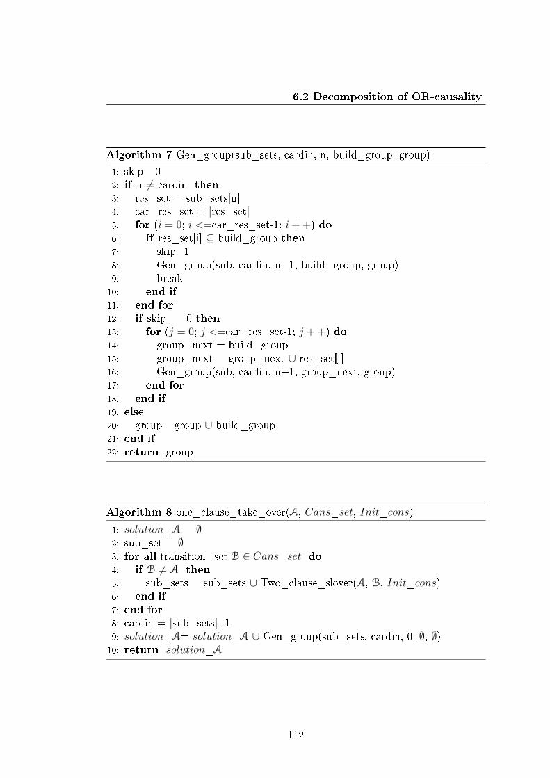
6.2 Decomposition of OR-causality
Algorithm 7 Gen_group(sub_sets, cardin, n, build_group, group)
1: skip =02: if n 6= cardin then3: res_set = sub_sets[n]4: car_res_set = |res_set|5: for (i = 0; i <=car_res_set-1; i++) do6: if res_set[i] ⊆ build_group then7: skip=18: Gen_group(sub, cardin, n+1, build_group, group)9: break
10: end if11: end for12: if skip ==0 then13: for (j = 0; j <=car_res_set-1; j ++) do14: group_next = build_group15: group_next = group_next ∪ res_set[j]16: Gen_group(sub, cardin, n+1, group_next, group)17: end for18: end if19: else20: group =group ∪ build_group21: end if22: return group
Algorithm 8 one_clause_take_over(A, Cans_set, Init_cons)
1: solution_A = ∅2: sub_set = ∅3: for all transition_set B ∈ Cans_set do4: if B 6= A then5: sub_sets = sub_sets ∪ Two_clause_slover(A, B, Init_cons)6: end if7: end for8: cardin = |sub_sets| -19: solution_A= solution_A ∪ Gen_group(sub_sets, cardin, 0, ∅, ∅)
10: return solution_A
112

6.2 Decomposition of OR-causality
groups for each candidate clause, where each restriction set represents the added
ordering restriction arcs in one subSTG. The top level algorithm for the decom-
position of an OR-causality relation involving a set of candidate transition sets
Cans_set with the initial ordering restriction set Init_cons is presented in Al-
gorithm 9.
Algorithm 9 OR_causality_decomposition (Cans_set, Init_cons)
1: solution = ∅2: for all Candidate_transition_set A ∈ Cans_set do3: solution = solution ∪ one_clause_take_over(A, Cans_set, Init_cons)4: end for5: return solution
When the solution group for one OR-causality is derived, the STG will be
decomposed into a set of subSTGs according to the restriction sets in the group.
One subSTG will be generated for each restriction set and an ordering restriction
arc will be inserted for each restriction pair in each restriction set.
For OR-causality relation in case 2, when one candidate clause takes respon-
sibility for causing the output transition, arcs will be added from all candidate
transitions in that clause to the output transition to indicate that these candi-
date transitions are the prerequisite transitions for the output transition. One
ordering restriction arc (marked with # symbol) will be added for one restriction
pair in each restriction set.
Figure 6.6 shows a gate o and its STG segment. This STG segment has an
OR-causality relation whose solution set is
113

6.2 Decomposition of OR-causality
x
zy o
mn
k
x+
y+
m+
o+
n+k+z+
(a) (b)
Figure 6.6: An OR-causality relation in case 2. (a) the gate and (b) its
local STG segment -
S =
Sx =
{
{x+ ≺ k+; x+ ≺ n+}{x+ ≺ z+; x+ ≺ n+}
Szk ={
{z+ ≺ x+; k+ ≺ x+; z+ ≺ n+; k+ ≺ n+}
Sn =
{
{n+ ≺ x+;n+ ≺ k+}{n+ ≺ x+;n+ ≺ z+}
The decomposition results for the OR-causality relation in Figure 6.6 (after
eliminating the redundant arcs) is presented in Figure 6.7. Diagram (a) in Fig-
ure 6.7 shows the subSTG corresponds to the restriction set {x+ ≺ k+; x+ ≺
n+}. Diagram (b) shows the subSTG corresponds to the restriction set {x+ ≺
z+; x+ ≺ n+}. Diagram (c) shows the subSTG corresponds to the restriction
set {z+ ≺ x+; k+ ≺ x+; z+ ≺ n+; k+ ≺ n+}. Diagram (d) shows the subSTG
corresponds to the restriction set {n+ ≺ x+;n+ ≺ k+}. Diagram (e) shows the
subSTG corresponds to the restriction set {n+ ≺ x+;n+ ≺ z+}.
For OR-causality relation in case 3, when one candidate clause c takes charge
of causing the output transition, arcs will be added from all candidate transitions
in this clause to the output transition to indicate that these candidate transitions
are the prerequisite transitions for the output transition. For all transitions t∗,
114
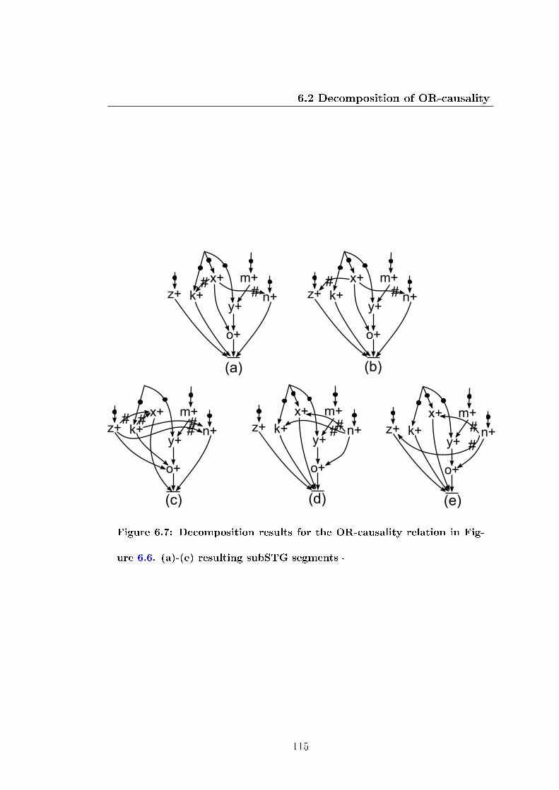
6.2 Decomposition of OR-causality
x+
y+
m+
o+
n+k+z+ ## x+
y+
m+
o+
n+k+z+ ##
x+
y+
m+
o+
n+k+z+ #x+
y+
m+
o+
n+k+z+ ### #
#
x+
y+
m+
o+
n+k+z+ #
#
(a) (b)
(c) (d) (e)
Figure 6.7: Decomposition results for the OR-causality relation in Fig-
ure 6.6. (a)-(e) resulting subSTG segments -
115

6.2 Decomposition of OR-causality
which are prerequisite transitions for the output transition in the original STG,
if t (if t∗ is t+) or t (if t∗ is t−) is not a literal of clause c, the arc t∗ ⇒ o∗ will
be relaxed. This is because unlike case 2, where all the prerequisite transitions of
o∗ are still prerequisite transitions after decomposition, if t or t is not a literal of
clause c, t∗ will not be the prerequisite transition any more and t∗ should become
concurrent with o∗. One ordering restriction arc (marked with # symbol) will be
added for one restriction pair in each restriction set.
x
y
om
n
px+
y+o+m+ n+
p+
(a) (b)
Figure 6.8: An OR-causality relation in case 3. (a) the gate and (b) its
local STG segment -
Figure 6.8 shows a gate o and its STG segment. This STG segment meets an
OR-causality relation whose solution set is
S =
Sx =
{
{x+ ≺ y+}{x+ ≺ m+; x+ ≺ n+}
Smy ={
{m+ ≺ x+; y+ ≺ x+;m+ ≺ n+}Sny =
{
{n+ ≺ x+; y+ ≺ x+;n+ ≺ m+}The decomposition results for the OR-causality relation in Figure 6.8 (af-
ter eliminating the redundant arcs) is presented in Figure 6.9. Diagram (a) in
Figure 6.9 shows the subSTG corresponds to the restriction set {x+ ≺ y+}. Dia-
116

6.3 Summary
gram (b) shows the subSTG corresponds to the restriction set {x+ ≺ m+; x+ ≺
n+}. Diagram (c) shows the subSTG corresponds to the restriction set {m+ ≺
x+; y+ ≺ x+;m+ ≺ n+}. Diagram (d) shows the subSTG corresponds to the
restriction set {n+ ≺ x+; y+ ≺ x+;n+ ≺ m+}.
x+
y+oymz nz
py#
x+
y+oymz nz
py ##
x+
y+oymz nz
py#
#
#
x+
y+oymz nz
py
#
#
#
(a) (b)
(c) (dm
Figure 6.9: Decomposition results for the OR-causality relation in Fig-
ure 6.8. (a)-(d) resulting subSTG segments -
6.3 Summary
This chapter analyzes the OR-causality relation in the relaxation case 2 or case 3
in detail and introduces the technique to decompose an STG into a set of subSTGs
when an OR-causality occurs. In each subSTG, one pull up/down function of a
117

6.3 Summary
gate is guaranteed to be enabled by one speci�ed clause. There are no OR-
causality relations in the subSTGs. Each subSTG is then processed in the �ow
described in chapter 5 and a gate will work properly if it works properly in every
subSTG.
118

Chapter 7
Results
This chapter presents the results of the theory proposed in Chapter 5. In the �rst
section, one example is used to demonstrate entire �ow of the proposed method
in detail and then the benchmark results for certain application examples are
presented.
7.1 Design example
The inputs of the proposed technique are one SI circuit together with its imple-
mentation STG. As an example, the block diagram and the STG speci�cation of
a 2-cycle FIFO controller(chu150 ) is presented in Figure 7.1. The speci�cation is
synthesized and then decomposed into simple gates using the tool petrify. The re-
sulting implementation STG and the circuit diagram are presented in Figure 7.2.
This implementation STG is an MG, so, it does not need to be decomposed any-
more. The local STG for each internal and output signal is then derived and
119
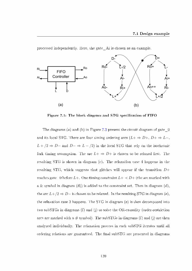
7.1 Design example
processed independently. Here, the gate_Ai is chosen as an example.
Ri
Ai
Ro
Ao
L D
D-
Ao-
Ai-
Ri+
L+
D+
Ao++
Ai+
Ri-
Ro-
L+/2
Ro+ L-L-/2
(a) (b)
FIFO
Controller
Figure 7.1: The block diagram and STG speci�cation of FIFO -
The diagrams (a) and (b) in Figure 7.3 present the circuit diagram of gate_0
and its local STG. There are four timing ordering arcs (L+ ⇒ D+, D+ ⇒ L−,
L + /2 ⇒ D− and D− ⇒ L − /2) in the local STG that rely on the isochronic
fork timing assumption. The arc L+ ⇒ D+ is chosen to be relaxed �rst. The
resulting STG is shown in diagram (c). The relaxation case 4 happens in the
resulting STG, which suggests that glitches will appear if the transition D+
reaches gate_0 before L+. One timing constraint L+ ≺ D+ (the arc marked with
a & symbol in diagram (d)) is added to the constraint set. Then in diagram (d),
the arc L+/2 ⇒ D− is chosen to be relaxed. In the resulting STG in diagram (e),
the relaxation case 3 happens. The STG in diagram (e) is then decomposed into
two subSTGs in diagrams (f) and (j) to solve the OR-causality (order-restriction
arcs are marked with a # symbol). The subSTGs in diagrams (f) and (j) are then
analyzed individually. The relaxation process in each subSTG iterates until all
ordering relations are guaranteed. The �nal subSTG are presented in diagrams
120

7.1 Design example
Ao
D
Ri
Ro
Ai
L
gate_0
gate_Ro
gate_Ai
gate_2
gate_3
w1
gate_4
gate_L
w2
w3 w4 w16
w5
w6w8
w7
w9 w10
w11
w12
w13
w14
w15
w17
D+
Ro+
Ao+
2-
3-
4+
L-
0-
Ri-
L+/2
D- 0+
Ro- 2+
Ao- L-/2
3+ Ai-
Ri+
4-
L+
Ai+
Figure 7.2: The implementation STG and circuit diagram of FIFO -
(i) and (k). One could see that there are two timing constraints (L+ ≺ D+
and D− ≺ L − /2) in the �nal subSTGs compared with four in the original
local STG, which indicates that the unnecessary timing orderings D+ ⇒ L− and
L+ /2 ⇒ D− are excluded during the relaxation process.
A timing constraint could then be changed into a delay constraint between a
wire and its adversary path by looking up the circuit and the entire STG shown
in Figure 7.2. The timing constraint D− ≺ L − /2 for gate_0 implies that the
transition D− from the environment propagating to gate_0 along the wire w3
should be faster than propagating along the adversary path wire w5, gate_2, w7,
gate_L and w14.
Each internal and output signal in this circuit are processed individually, and
121

7.1 Design example
0-
L- D+
L+
L-/2L+/2D-
0+
Relax L+ D+
Relax L+/2 D-
Case 3 STG decompositio
n
subSTG 1
Implementation
STG projecting
on {D, L, 0}
gate_0
L
(a) (b) (c)
(d) (e)
(f)
D0-
L- D+
L+
L-/2L+/2D-
0+
0-
L- D+
L+
L-/2L+/2D-
0+
&
Case 4
timing constraint
L+ < D+
0-
L- D+
L+
L-/2L+/2 D-
0+
&
0-
L- D+
L+
L-/2L+/2D-
0+
&
#
(j)
0-
L- D+
L+
L-/2L+/2
D-
0+
&
#
Case 3 STG decomposition
subSTG 2
Relax D- L-/2
0-
L- D+
L+
L-/2L+/2 D-
0+
&
#
(g)Case 4
timing constra
int
D- < L-/2
0-
L- D+
L+
L-/2L+/2D-
0+
&
#
(h)
0-
L-
D+ L+
L-/2L+/2D-
0+
&
#
Relax D+ L-
Case 1
& &
(i)
0-
L-
L+
L-/2L+/2
D-
0+
#
(k)
Relax D+ L-
Case 1
D+ &
Figure 7.3: The STG relaxation procedure of the gate_0 -
122

7.1 Design example
the delay constraints for this circuit to work correctly are shown in Table 7.1.
Most constraints in Table 7.1 are quite loose, which could be considered to have
been ful�lled already. When some constraints are considered strong, delays need
to be padded to ful�ll these constraints.
In this example, the adversary paths, whose levels are deeper than �ve (adver-
sary path involves more than two gates), or which pass through the environment
(the delay for the response from the environment is usually larger than a wire de-
lay in the circuit), are considered to be ful�lled already. There are two constraints
left, w15+ < w14+, gate_0+, w4+ and w3− < w5−, gate_2+, w7+, gate_L−, w14−.
These two constraints could be guaranteed by padding delays on wire w4 and w14.
A closer look at Table 7.1 reveals that each constraint only involves unidirec-
tional transitions on the adversary paths. This suggests that less performance
penalty would be introduced if the delays padded on adversary paths only de-
lay the required unidirectional transition. This could be achieved by using the
current-starved delay[65][66]. Two examples of the current-starved delay are pre-
sented in Figure 7.4. The current-starved delay uses a control voltage V to control
the charge/discharge current to control the delay magnitude of falling/rising tran-
sitions. The delay presented in diagram (a) in Figure 7.4 could delay the rising
transition for a given time but has little e�ect on the falling transition; while the
current-starved delay in (b) could delay the falling transition for a given time but
has little e�ects on the rising transition.
123

7.2 Simulation and Analysis
Table 7.1: List of timing constraints
wire ≤ adversary pathw15+ w14+, gate_0+, w4+w14+ w3+, ENV, w17+w3- w5-, gate_2+, w7+, gate_L-, w14-w6- w9-, gate_3+, w10+, gate_4-, w12-,gate_L+, w17+,ENV, w5+w5- w1+, gate_Ro+, w2+, ENV, w6+w8+ w1+, gate_Ro+, w2+, w6+, gate_2-, w7-, gate_L+, w8+,
gate_3-, w10-, gate_4+, w12+, gate_L-, w14-, gate_0-, w4-,gate_Ai+, ENV, w16+, w13-, gate_L+, w17+, w1-, gate_Ro-,w2-, w9-
w9+ w6+, gate_2-, w7-, gate_L+, w17+, ENV, w8-w13+ w11+, gate_4-, w12-, gate_L+, w17+, ENV, w1+, Ro+, w2+,
ENV, w6+, gate_2-, w7-w11- w13-, gate_L+, w17+, ENV, w1-, Ro-, w2-, w9-, gate_3+,
w10+
7.2 Simulation and Analysis
The FIFO circuit is put through SPICE simulation using ASU Predictive Tech-
nology Model bulk CMOS model library from 90nm to 32nm [67]. The theoretical
error rates due to the failure of the isochronic fork as the process shrinks and the
performance penalty due to the padding are tested. When calculating the error
rate, only the glitches caused by the wire delays are considered. Failures caused
by the variation of the threshold are not considered. The error rate of the cir-
cuit is pessimistically calculated when any gate in the FIFO circuit glitches. As
the length of local interconnection decreased as process shrinks, the relative wire
length is used to compare the error rates between di�erent processes. The wire
length is changed into units of gate pitches and the interconnection distribution
function of the wire length in a circuit is calculated using the formula in [68]:
124

7.2 Simulation and Analysis
inp outp
V
V
inp outp
(a) (b)
Figure 7.4: The current starved delays. (a) controlled delay for rising
transition and (b) controlled delay for falling transition -
for 1 ≤ l ≤√N :
i(l) =αk
2Γ(
l3
3− 2
√Nl2 + 2Nl)l(2p−4)
for√N ≤ l <
√2N :
i(l) =αk
6Γ(2
√N − l)3l(2p−4)
where
Γ =2N(1−Np−1)
−Np 1+2p−22p−1
p(2p−1)(p−1)(2p−3)− 1
6p+ 2
√N
2p−1− N
p−1
Where N is the number of gates and the experience constant is set to k=3, p=0.85
and α=23respectively. The error rate for each gate is conservatively calculated
as:
ER =
∫ 2√N
error_length
i(l)dl · (∫ short_wire_length
0
i(l)dl)m
Where error_length is the units of gate pitch from which this gate starts to
glitch, short_wire_length is the length that we assume the wires in the adver-
125

7.2 Simulation and Analysis
sary path will not exceed (about 20 gate pitches) and m is the number of wires
segments in the adversary path.
90nm 65nm 45nm 32nm0
2%
4%
6%
8%
10%
12%
Circ
uit e
rror
rat
e
Process
un−bufbuf−1
Figure 7.5: The trend of error rate as the technology shrinks -
Figure 7.5 shows the trends of error rate as the process shrinks in one million-
gate scale circuit, un-buf indicates the case where bu�ering is not used on long
wires and buf-1 depicts the error rate when one bu�er is inserted into the "direct
wire" and no bu�ers inserted into its "adversary path" (The error rate will in-
crease signi�cantly when a bu�er is inserted into the "direct wire". Please refer
to the section 4.2.3 for the detailed analysis).
The Figure 7.6 shows the trends of the error rate as the scale increases from
0.5 million to 4 million under the 90nm process.
As can be seen from these �gures, the error rate increases as the technology
shrinks and the bu�er insertion technique will increase the error rate signi�cantly.
126

7.2 Simulation and Analysis
90nm−0.5M 90nm−1M 90nm−2M 90nm−4M0
1%
2%
3%
4%
5%
6%
7%
8%
9%
Circ
uit e
rror
rat
e
Scale
un−bufbuf−1
Figure 7.6: The trend of error rate as the scale increases -
Also, the error rate increases remarkably with the scale of circuit. The results
suggest that SI circuits will become less safe in the future.
The Figure 7.7 shows the delay penalty to eliminate all the glitches in one mil-
lion gates scale using di�erent padding methods (bu�er and one-direction current-
starved delay). The delays are inserted on wire w4 and w14 to just counter the
maximum wire length delay, the environment is assumed to be zero delay and the
delay penalty is calculated as the maximum latency increase in the slowest STG
cycle.
127

7.3 Benchmarks
90nm 65nm 45nm 32nm0%
5%
10%
15%
20%
25%
30%
35%
40%
45%
Del
ay p
enal
ty
current−starvedrepeater
Figure 7.7: The delay penalty -
7.3 Benchmarks
This section describes automated tool and presents the benchmark results on a
set of popular SI circuits.
7.3.1 Description of the Tool
The technique presented in Chapter 5 has been implemented in the tool Check_hazard,
which reads an STG as the circuit speci�cation and a restricted EQN �le as the
circuit description.
The STG to the tool is in the astg format as was used in the tools petrify
[60] and sis [69], since the astg format is widely used in the tools related to the
synthesis and veri�cation of SI circuits. This format will not be introduced in
128

7.3 Benchmarks
detail here. Currently, the circuit speci�cation format used in the tool is in a
restricted EQN format. In this format, each line contains an equation in the
sum of product form to specify the pull-up function of one gate in the circuit.
No brackets are allowed. The literals in each product term are connected by
the symbol ∗ and di�erent product terms are connected by the symbol +. The
negation of a signal is su�xed by "'". An equation is terminated with a ";". The
synthesized netlists from some popular tools such as petrify and sis might need
to be preprocessed before being input to the tool. For example, for a C-element
with the input signal A and the negation of signal B, the equation should be like:
C = A*B' + A*C + B'*C;
The equation C = A*B' + C* (A+B'); is not correct because it contains a pair
of brackets. The example of an STG in the astg format is shown below:
129

7.3 Benchmarks
.model imec-ram-read-sbuf
.inputs req precharged prnotin wenin wsldin
.outputs ack wsen prnot wen wsld
.internal csc0 map0 i0 i2 i4 i8
.graphreq+ i4+i4+ prnot+prnot+ prnotin+precharged+ prnot+prnotin+ wen+wen+ precharged- wenin+precharged- i0-i0- ack+wenin+ i0-ack+ req-req- i8+ wen-i8+ csc0-wen- wenin-wsen- wenin-wenin- wsld+ i4- i0+i0+ ack-i4- prnot-wsld+ wsldin+ precharged+wsldin+ csc0+prnot- prnotin- precharged+prnotin- i8-i8- csc0+wsld- wsldin-wsldin- wsen+ map0+ack- req+wsen+ req+csc0+ wsld- i2-i2- wsen+csc0- map0-map0+ ack-map0- i2+i2+ wsen-.marking { <i4+,prnot+> <precharged+,prnot+> }.end
A circuit speci�cation in the restricted EQN format is shown below:
i0 = precharged + wenin';ack = i0' + map0';i2 = csc0' * map0';wsen = wsldin' * i2';i4 = wenin + req;prnot = i4* precharged + i4 * prnot + precharged * prnot;wen = req * prnotin;wsld = wenin' * csc0';i8 = req' * prnotin;csc0 = i8' *wsldin + i8' * csc0;map0 = wsldin' * csc0;
A command line to run the tool is "Check_hazard STG.g EQN.eqn". The tool
130
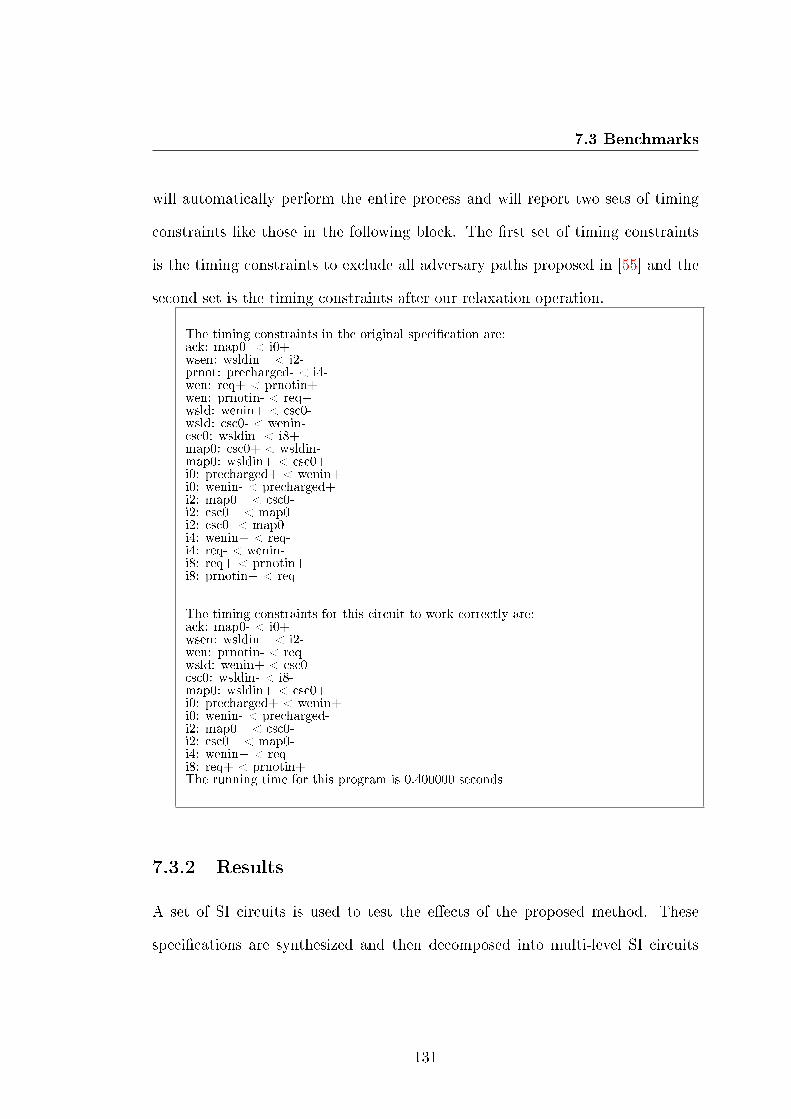
7.3 Benchmarks
will automatically perform the entire process and will report two sets of timing
constraints like those in the following block. The �rst set of timing constraints
is the timing constraints to exclude all adversary paths proposed in [55] and the
second set is the timing constraints after our relaxation operation.
The timing constraints in the original speci�cation are:ack: map0- < i0+wsen: wsldin+ < i2-prnot: precharged- < i4-wen: req+ < prnotin+wen: prnotin- < req+wsld: wenin+ < csc0-wsld: csc0- < wenin-csc0: wsldin- < i8+map0: csc0+ < wsldin-map0: wsldin+ < csc0+i0: precharged+ < wenin+i0: wenin- < precharged+i2: map0+ < csc0-i2: csc0+ < map0+i2: csc0- < map0-i4: wenin+ < req-i4: req- < wenin-i8: req+ < prnotin+i8: prnotin+ < req-
The timing constraints for this circuit to work correctly are:ack: map0- < i0+wsen: wsldin+ < i2-wen: prnotin- < req+wsld: wenin+ < csc0-csc0: wsldin- < i8-map0: wsldin+ < csc0+i0: precharged+ < wenin+i0: wenin- < precharged-i2: map0+ < csc0-i2: csc0+ < map0-i4: wenin+ < req-i8: req+ < prnotin+The running time for this program is 0.400000 seconds
7.3.2 Results
A set of SI circuits is used to test the e�ects of the proposed method. These
speci�cations are synthesized and then decomposed into multi-level SI circuits
131

7.3 Benchmarks
with each gate containing no more than 4 input signals using the tool petrify [60].
The benchmark results are obtained on a 2.4Ghz personal computer. The Table
6.2 shows the comparison of generated timing constraints between the proposed
method and the timing assumptions proposed in [55], which is currently the
weakest formally proved set of conditions.
The column "NO. of adv. before" presents the number of timing constraints
before our relaxation process. The timing constraints before our process are
equal to the timing constraints to exclude all adversary paths in an SI circuit as
is proposed in [55] . The column "NO. of adv. after" presents the number of
timing constraints after our relaxation process. The column "NO. of ≤ 5 level
adv. before" presents the number of timing constraints to exclude the adversary
paths whose level is less than or equal to 5 (two gates appear in the adversary
path) and the column "NO. of ≤ 5 level adv. after" presents the number of timing
constraints in three and �ve level in our technique. The column "NO. of ≤ 3 level
adv. before" presents the number of timing constraints to exclude the adversary
paths whose level is three (one gate appears in the adversary path). The column
"NO. of ≤ 3 level adv. after" presents the number of timing constraints in three
level in our technique. As can be seen from this table, the relaxation reduces by
around 40% of unnecessary constraints in all these three aspects. Also, from the
table, one could �nd that the computational time does not increase signi�cantly
as the number of states 1 increases.
1The number of reachable states shown in this table is the number of states reached by thecircuit when the isochronic fork timing assumption is not relaxed. The reachable states wouldboost signi�cantly when the isochronic fork timing assumption is relaxed.
132

7.3
Benchmarks
Name NO. of
in
NO. of
out
NO. of
gate
NO. of
states
NO. of adv.
before
NO. of adv.
after
NO. of ≤
5 level adv.
before
NO. of ≤
5 level adv.
after
NO. of ≤
3 level adv.
before
NO. of ≤
3 level adv.
after
CPU
time (s)
adfast 3 3 7 94 10 6 4 2 0 0 0.04
atod 3 3 5 28 14 9 10 4 3 1 0.01
chu 133 3 4 7 41 10 6 2 1 1 1 0.04
converta 2 3 7 36 20 10 10 6 8 4 0.1
ebergen 2 3 5 24 10 6 5 5 2 2 0.01
�fo (chu 150) 3 3 7 64 14 9 5 3 4 2 0.05
imec-nak-pa 4 5 10 110 16 11 8 5 1 1 0.24
imec-ram-read-sbuf 5 5 11 112 19 12 4 2 2 1 0.40
imec-sbuf-read-ctl 2 4 8 32 12 6 3 3 2 2 0.06
mp-forward-pkt 3 5 8 44 13 8 1 1 0 0 0.1
nowich 3 3 8 43 10 5 2 1 1 0 0.12
trimos-send 3 6 15 2023 35 25 15 11 12 8 0.12
vbe5c 3 6 5 37 8 4 6 1 4 1 0.12
Total ratio after/before = 63.9 % after/before = 60.0% after/before = 57.5 %
Table 7.2: Comparison of the timing constraints
133

7.4 Summary
7.4 Summary
This chapter �rst demonstrates the relaxation process of the proposed method
using an FIFO controller example. The example is then simulated to study the
error rate when the technology develops. Even though the threshold voltage
variations are not considered, error rate increases as the semiconductor feature
size shrinks. Also, a set of popular SI circuits is used to test the proposed method.
The benchmark results suggest that the proposed method excludes around 40%
unnecessary timing constraints compared with the previous research on this issue.
134
Chapter 8
Conclusion and Future Work
This chapter concludes our work and discusses the possible promotions for the
proposed method.
8.1 Conclusion
As the semiconductor technology shrinks, process variations become a big ob-
stacle to the circuit design. The synchronous design, which needs to distribute
the clock signal throughout the whole circuit, faces severe challenges. The asyn-
chronous design suggests a promising design method for the IC design industry
in the coming few decades. The SI design paradigm is more interesting in the
variation tolerance aspect compared with other asynchronous design paradigms.
Not only because it has the strongest variation tolerance ability for the most
speci�cations, but also because it has comparatively better EDA tool support.
However, any asynchronous circuit which is not DI will malfunction if certain
135

8.1 Conclusion
timing requirements are not met. Any SI circuit should be veri�ed �rst before
implementation.
Current veri�cation methods for SI circuits are mainly focused on checking
whether an SI circuit works properly under the isochronous fork timing assump-
tion; that is whether the circuit is functionally conformant to the its speci�cation
and is SI. However, as the process shrinks, the isochronic fork timing assumption
is no longer reliable. It is required that the timing veri�cation technique should
also consider the situation where the isochronic fork assumption is no longer
guaranteed. The timing veri�cation is a computationally expensive task. It is
especially true for asynchronous circuits which do not have latches to isolate the
entire circuit into smaller blocks. This work proposes a technique to derive a set
of timing constraints that are su�cient for an SI circuit to work correctly when
the isochronic fork timing assumption is relaxed into the intra-operator fork tim-
ing assumption. The whole veri�cation task is divided into a set of smaller tasks
to avoid exploring the entire reachability space. The high level model (STG) is
used to describe the behavior and manipulate the transition causalities in an SI
circuit; while, the low level model (SG) is used to check whether hazards would
appear in the circuit under a given environment. Each turn, the relaxation pro-
cess modi�es the causality of two ordered transitions into concurrent to include
the states that will be reached when the arriving order of two events in the circuit
is reversed. Then the SG of the resulting STG will be checked to see whether it
contains hazards. If it does, one timing constraint will be generated to guarantee
the original ordering of the two events; if it does not, the resulting STG will be
accepted which allows the occurrence of the two events in any order. The timing
136

8.2 Future work
assumptions in the resulting STG will have one less adversary path compared
with the original one. The generated timing constraints are signi�cantly weaker
than the existing proved conditions. Around 40% unnecessary timing constraints
are excluded after local STG relaxation.
The main contributions of the proposed method are:
1) It corrects some wrong conclusions given by previous researchers about the
weakest timing assumption in SI circuits.
2) It introduces a hazard checking criterion for SI circuits when the isochronic
fork timing assumption is relaxed into the intra-operator fork timing assumption.
3) It proposes a polynomial complexity method for generating a set of timing
constraints for an SI circuit to work properly under the intra-operator fork timing
assumption. The proposed method checks the hazards of each gate at its local
STG. This means that the complexity of hazard checking task is linear to the
number of gates in an SI circuit. Also, the complexity of deriving the local STGs
for all gates in an SI circuit is polynomial to the number of gate in the circuit if
the number of free-choice places in its STG is considered to be a constant.
This work could be improved if the following questions are answered.
8.2 Future work
8.2.1 Non-free-choice place
The relaxation process in the proposed technique requires that the local STG
of the gate must be an MG, where transitions have explicit ordering relations.
137

8.2 Future work
The technique proposed in [8], which could decompose a live and safe free-choice
STG into a set of MGs, requires the original STG to be a free-choice one and
a guaranteed method of decomposing any STG into a set of equivalent MG's
cannot be found in the literature. One solution to this problem is to change a
non-free-choice STG into a free-choice STG by writing its SG and then deriving
a free-choice STG from this SG using the technique proposed in [49], which has
been implemented in the petrify tool. One example is shown in Figure 8.1.
However, the derived free-choice STG might contain too many choice places.
The technique proposed in [8] uses brute force to enumerate all possible MG
components; so, the number of MGs grows exponentially with respect to the
number of free-choice places in the STG. If the STG contains too many choice
places, decomposing this STG becomes impractical.
Future research could be carried out to �nd a technique that could struc-
turally decompose a less restricted class of PN into a set of MGs, thus avoiding
introducing too many choice places during transforming the original STG into a
free-choice STG.
8.2.2 Not pure SI circuits
Many synthesis techniques [70] [71] [72] involve timing assumptions during the
logic synthesis to improve the performance. The synthesized circuits are then no
longer pure SI circuits. Some timing assumptions involved in these synthesis tech-
nique could be expressed by relative timing arcs, for example, the concurrency
reduction arcs in [50]. Some timing assumptions could be expressed by decom-
138
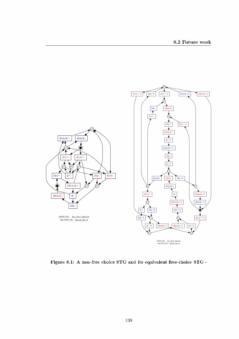
8.2 Future work
INPUTS: dsr,dsw,ldtack
OUTPUTS: dtack,lds,d
p0
dtack-
dsr- dsw-
p 2
d t a c k+
d s r + d sw+
p 1
p 5 p 6 p7
p4
l d s+ d +
ld t ack+ p 3
d-
lds-
ldtack-
INPUTS: dsr,dsw,ldtack
OUTPUTS: dtack,lds,d
p0
ldtack-/3d sw+ / 2 d s r+ / 2
p 2
p11
p5
dtack-/2lds-/3
ldtack-lds-
p8
l d s+
d s r +
ld t ack+
ds r+ / 1
d+ / 1
d t a ck+ /1
dsr-
d-/1
p1
dtack- lds-/4
p6
dsw-
p9
d sw+ ldtack-/4
d t a c k+
d-
p10 dtack-/1
d + lds-/2
ld tack+/1
d sw+ / 1lds-/1
lds+ /1
p7
ldtack-/2d+ / 3
p 3 p 4
d+ / 2ldtack-/1
(b)
Figure 8.1: A non-free choice STG and its equivalent free-choice STG -
139

8.2 Future work
posing the original STG into a set of component STGs and then using timing arcs
to restrict the �ring sequences (similar the OR-causality decomposition), like the
indistinguishable �ring timing assumption in [50]. For those timing assumptions
that are not easy to express with timing arcs, one possible approach is to specify
a set of states such that these states are not hazardous states even if they are not
timing conformant to the function of the gate.
140

References
[1] G. E. Moore. Cramming more components onto integrated circuits.
Electronics Magazine, 1965. 3
[2] M. Donno, E. Macii, and L. Mazzoni. Power-aware clock tree plan-
ning. Proceedings of ISPD'04, 2004. 3
[3] V. Tiwari, D. Singh, S. Rajgopal, G. Mehta, R. Patel, and
F. Baez. Reducing Power in High-Performance Microprocessors.
Proceedings of DAC'98, 2004. 3
[4] M. Favalli and L. Benini. Analysis of glitch power dissipation in
CMOS ICs. Proceedings of the 1995 international symposium on Low
power design, 2004. 4
[5] ITRS2007. http://www.itrs.net/. 2007. 5
[6] J. Sparso and S. Furber. Principles of Asynchronous Circuit De-
sign: A Systems Perspective. Kluwer Academic Publishers, 2001. 5, 13,
15
141

REFERENCES
[7] A. J. Martin. The Limitations to Delay-Insensitivity in Asyn-
chronous Circuits. Sixth MIT Conference on Advanced Research in VLSI,
1990. 7
[8] M. Hack. Analysis of production schemata by Petri nets. Technical
Report, Massachusetts Institute of Technology Cambridge, 1972. 9, 53, 54,
84, 138
[9] L. Lavagno. Synthesis and Testing of Bounded Wire Delay Asyn-
chronous Circuits from Signal Transition Graphs. PhD thesis, U.C.
Berkeley, 1992. 11, 30, 89
[10] W. B. Toms and D. A. Edwards. E�cient Synthesis of Speed-
Independent Combinational Logic Circuits. Proceedings of the Asia
and South Paci�c Design Automation Conference, 2005. 16
[11] Y. Zhou, D. Sokolov, and A. Yakovlev. Cost-aware synthe-
sis of asynchronous circuits based on partial acknowledgement.
Proceedings of International Conference on Computer-Aided Design, 2006.
16
[12] A. J. Martin. Asynchronous datapaths and the design of an asyn-
chronous adder. Formal Methods in System Design, 1992. 16
[13] D.A. Huffman. The synthesis of sequential switching circuits. J.
Franklin Inst., 1954. 16, 17
142

REFERENCES
[14] S. H. Unger. Asynchronous sequential switching circuits.
Wiley-interscience, John Wiley & Sons, Inc., 1969. 17
[15] S. M. Nowick. Automatic synthesis of burst-mode asynchronous
controllers. Technical Report, CSL-TR-95-686, Stanford University, 1995.
17
[16] Robert M. Fuhrer, Niraj K. Jha, Bill Lin, Luis Plana, and et al.
MINIMALIST: An Environment for the Synthesis, Veri�cation
and Testability of Burst-Mode Asynchronous Machines, 1999. 18
[17] K. Y. Yun and D. L. Dill. Unifying Synchronous/Asynchronous
State Machine Synthesis. Proceedings of the IEEE/ACM International
Conference on Computer-Aided Design, 1993. 18
[18] K. Y. Yun and D. L. Dill. Automatic synthesis of extended burst-
mode circuits. I. (Speci�cation and hazard-free implementations).
IEEE Transactions on Computer-Aided Design of Integrated Circuits and
Systems, 1999. 18
[19] K. Y. Yun and D. L. Dill. Automatic synthesis of extended burst-
mode circuits: part II (automatic synthesis). IEEE Transactions on
Computer-Aided Design of Integrated Circuits and Systems, 1999. 18
[20] D. E. Muller and W. S. Bartky. A theory of asynchronous circuits.
Proceedings of an International Symposium on the Theory of Switching,
1959. 19
143

REFERENCES
[21] D. E. Muller. Asynchronous logics and application to information
processing. Proceedings of the Symposium on the Application of Switching
Theory in Space Technology, 1963. 19
[22] A. J. Martin. The design of a delay-insensitive microprocessor: an
example of circuit synthesis by program transformation. Hardware
Speci�cation, Veri�cation and Synthesis: Mathematical Aspects, 1989. 19,
38
[23] J. A. Brzozowski and J. Ebergen. On the Delay-Sensitivity of
Gate Networks. IEEE Transactions on Computers, 1992. 19
[24] R. Manohar and A. J. Martin. Quasi-delay-insensitive circuits are
Turing-complete. Second International Symposium on Advanced Research
in Asynchronous Circuits and Systems, 1995. 20
[25] A. J. Martin. Programming in VLSI: From Communicating Pro-
cesses to Delay-Insensitive Circuits. Developments in Concurrency and
Communication, 1990. 20
[26] S. H. Unger. Hazards, Critical Races, and Metastability. IEEE
Transactions on Computers, 1995. 20
[27] K. S. Stevens, S. Rotem, R. Ginosar, P. Beerel, C. J. Myers,
K. Y. Yun, R. Kol, C. Dike, and M. Roncken. An Asynchronous
Instruction Length Decoder. IEEE Journal of solid-state circuits, 2001.
24
144

REFERENCES
[28] A. Davis, B. Coates, and K. Stevens. The Post O�ce experience:
Designing a large asynchronous chip. In Proceeding of the Twenty-Sixth
Hawaii International Conference on System Sciences, 1993. 24
[29] P. A. Beerel and T.H.-Y. Meng. Automatic Gate-Level Syn-
thesis of Speed-Independent Circuits. In Proceeding of IEEE/ACM
International Conference on Computer-Aided Design, 1992. 24
[30] E. Pastor, J. Cortadella, A. Kondratyev, and O. Roig. Struc-
tural methods for the synthesis of speed-independent circuits. IEEE
Transactions on Computer-Aided Design, 1998. 24
[31] D. Edwards and A. Bardsley. Balsa: An Asynchronous Hardware
Synthesis Language. The Computer Journal, 2002. 24
[32] D. Sokolov, A. Bystrov, and A. Yakovlev. Direct Map-
ping of Low-Latency Asynchronous Controllers From STGs.
Computer-Aided Design of Integrated Circuits and Systems, IEEE
Transactions on, 2007. 24
[33] D. L. Shang, F. Burns, A. Koelmans, A. Yakovlev, and F. Xia.
Asynchronous system synthesis based on direct mapping using
VHDL and Petri nets. IEE Proceedings - Computers and Digital
Techniques, 2004. 24
[34] F. P. Burns, D. L. Shang, A. Koelmans, and A. Yakovlev. An
Asynchronous Synthesis Toolset Using Verilog. Design, Automation
and Test in Europe Conference and Exposition, 2004. 24
145

REFERENCES
[35] S. M. Burns. General Conditions for the Decomposition of
State Holding Elements. Asynchronous Circuits and Systems, IEEE
International Symposium on, 1996. 24
[36] A. Kondratyev, M. Kishinevsky, J. Cortadella, L. Lavagno, and
Alex Yakovlev. Technology mapping for speed-independent cir-
cuits: decomposition and resynthesis. In Proceeding of International
Symposium on Advanced Research in Asynchronous Circuits and Systems,
1997. 24
[37] A. Kondratyev, J. Cortadella, M. Kishinevsky, L. Lavagno, and
Alexander Yakovlev. Logic decomposition of speed-independent
circuits. In Proceedings of the IEEE, 1999. 24
[38] V. Khomenko. Model Checking Based on Pre�xes of Petri Net
Unfoldings. PhD thesis, University of Newcastle upon Tyne, 2003. 24, 49
[39] O. Roig, J. Cortadella, and E. Pastor. Hierarchical gate-level
veri�cation of speed-independent circuits. Proceeding of Second
Working Conference on Asynchronous Design Methodologies, 1995. 24, 49,
51
[40] I. Poliakov, A. Mokhov, A. Rafiev, D. Sokolov, and A. Yakovlev.
Automated veri�cation of asynchronous circuits using circuit
Petri nets. Proceedings of the 14th IEEE International Symposium on
Asynchronous Circuits and Systems, 2008. 24, 49, 51
146
REFERENCES
[41] D. L. Dill. Trace Theory for Automatic Hierarchical Veri�cation
of Speed-independent Circuits. MIT Press, 1989. 24
[42] P. A. Beerel, J. Burch, and T. H. Y. Meng. E�cient veri�cation
of determinate speed-independent circuits. Proceedings of the 1993
IEEE/ACM international conference on Computer-aided design, 1993. 24
[43] O. Roig, J. Cortadella, M. A. Pena, and E. Pastor. Automatic
generation of synchronous test patterns for asynchronous circuits.
In Proceeding of ACM/IEEE Design Automation Conference, 1997. 24
[44] C. A. Petri. Kommunikation mit automaten. PhD thesis, University
of Bonn, 1962. 25
[45] T. Murata. Petri nets: Properties, analysis and applications.
PROCEEDINGS OF THE IEEE, 1989. 27
[46] J. Desel and J. Esparza. Free choice Petri nets. Cambridge University
Press, 1995. 27
[47] L. Rosenblum and A. Yakovlev. Signal graphs: From self-timed to
timed ones. Proceedings of International Workshop on Timed Petri Nets,
1985. 28, 30
[48] T. A. Chu. Synthesis of self-timed VLSI circuits from graph-
theoretic speci�cations. PhD thesis, MIT Laboratory for Computer
Science, 1987. 28, 31, 84
147

REFERENCES
[49] J. Cortadella, M. Kishinevsky, L. Lavagno, and A. Yakovlev.
Deriving Petri nets from �nite transition systems. Computers, IEEE
Transactions on, 1998. 29, 138
[50] J. Cortadella, M. Kishinevsky, A. Kondratyev, L. Lavagno, and
A. Yakovlev. Logic Synthesis of Asynchronous Controllers and
Interfaces. Springer-Verlag, 2002. 31, 35, 36, 138, 140
[51] K. Van Berkel, F. Huberts, and A. Peeters. Stretching quasi de-
lay insensitivity by means of extended isochronic forks. Proceedings
of ASYNC '95, 1995. 35
[52] C. Piguet. Supplementary condition for STG-designed speed-
independent circuits. Electronics Letters, April 1998. 35, 36
[53] Kees van Berkel. Beware the Isochronic Fork. INTEGRATION, The
VLSI Journal, 1992. 35, 37
[54] N. Sretasereekul and T. Nanya. Eliminating isochronic-fork con-
straints in quasi-delay-insensitive circuits. Proceedings of the 2001
Asia and South Paci�c Design Automation Conference, 2001. 35, 41, 49
[55] S. Keller, M. Katelman, and A. J. Martin. A Necessary
and Su�cient Timing Assumption for Speed-Independent Cir-
cuits. Proceedings of Asynchronous Circuits and Systems, International
Symposium on, 2009, 2009. 35, 42, 45, 46, 50, 59, 131, 132
148

REFERENCES
[56] C. Piguet. Logic synthesis of race-free asynchronous CMOS cir-
cuits. IEEE J. Solid-State Circuits, March 1991. 37
[57] N. Starodoubtsev and S. Bystrov. Behavior and Synthesis of
Two-Input Gate Asynchronous Circuits. Proceedings of the 11th IEEE
international Symposium on Asynchronous Circuits and Systems, March
2005. 37
[58] L. Lin and W. Burleson. Analysis and mitigation of process varia-
tion impacts on Power-Attack Tolerance. Proceedings of Proceedings
of the 46th Annual Design Automation Conference, 2009. 38
[59] H. Saito, A. Kondratyev, J. Cortadella, L. Lavagno, and
A. Yakovlev. What is the cost of Delay Insensitivity. Proceedings
of the 1999 IEEE/ACM international conference on Computer-aided design,
1999. 49
[60] J. Cortadella, M. Kishinevsky, A. Kondratyev, L. Lavagno,
and A. Yakovlev. Petrify: A Tool for Manipulating Concurrent
Speci�cations and Synthesis of Asynchronous Controllers. IEICE
TRANSACTIONS on Information and Systems, 1996. 52, 128, 132
[61] M. Schafer, W. Vogler, and P. Jancar. Determinate STG De-
composition of Marked Graphs. Applications and Theory of Petri Nets
2005, 26th International Conference, 2005. 68, 69, 71
[62] M. Diaz. Petri Nets: Fundamental Models, Veri�cation and Ap-
plications. Wiley-ISTE, 2009. 69
149

REFERENCES
[63] A. Yakovlev, M. Kishinevsky, A. Kondratyev, and L. Lavagno.
OR causality: Modelling and hardware implementation.
Applications and Theory of Petri Nets 1994, International Conference, 1994.
75, 77
[64] A. Yakovlev, M. Kishinevsky, A. Kondratyev, L. Lavagno, and
M. Pietkiewicz-Koutny. On the models for asynchronous circuit
behaviour with OR causality. Formal Methods in System Design, 1996.
75, 77
[65] M. G. Johnson and E. L. Hudson. A variable delay line PLL
for CPU-coprocessor synchronization. IEEE Journal of Solid-State
Circuits, 1988. 123
[66] M. Maymandi-Nejad and M. Sachdev. A Digitally Programmable
Delay Element: Design and Analysis. IEEE TRANSACTIONS ON
VERY LARGE SCALE INTEGRATION SYSTEMS, 2003. 123
[67] http://ptm.asu.edu/. 124
[68] J. A. Davis, V. K. De, and J. D. Meindl. A stochastic wire-length
distribution for gigascale integration (GSI). IEEE Transactions on
Electron Devices, 1998. 124
[69] E. M. Sentovich, K. J. Singh, L. Lavagno, C. Moon, R. Mur-
gai, A. Saldanha, H. Savoj, P. R. Stephan, R. K. Brayton, and
A. Sangiovanni-vincentelli. SIS: A System for Sequential Circuit
Synthesis. technique report, 1992. 128
150

REFERENCES
[70] J. Cortadella, M. Kishinevsky, S. M. Burns, A. Kondratyev,
L. Lavagno, K. S. Stevens, A. Taubin, and A. Yakovlev. Lazy
Transition Systems and Asynchronous Circuit Synthesis with Rel-
ative Timing Assumptions. In IEEE Transactions on CAD, 2002. 138
[71] K. S. Stevens, S. Rotem, S. M. Burns, J. Cortadella, R. Gi-
nosar, M. Kishinevsky, and M. Roncken. CAD Directions for High
Performance Asynchronous Circuits. In Proceedings of the Digital
Automation Conference, 1999. 138
[72] P. Vanbekbergen, G. Goossens, and B. Lin. Modeling and Synthe-
sis of Timed Asynchronous Circuits. In Proceedings of the European
Design Automation Conference, 1994. 138
151

Index
adversary path, 43
adversary path timing assumption, 43
AND-causality, 90
autonomous circuits, 14
burst mode, 15
circuit, 14
clause, 12
cover, 12
irredundant prime cover, 12
o�-set cover, 12
on-set cover, 12
prime cover, 12
redundant cover, 12
cube, 12
delay, 13
bounded delay, 13
inertial delay, 13
pure delay, 13
unbounded delay, 13
delay-insensitive, 19
environment, 14
fundamental mode, 15
gate, 11
glitch, 20
Hu�man style, 16
implicant, 12
prime implicant, 12
input state, 11
input-output mode, 15
inter-operator fork, 41
intra-operator fork, 41
isochronic fork, 23
literal, 12
logic function, 11
marking
marking set, 26
Muller style, 18
o�-set, 11
on-set, 11
OR-causality, 80, 90
Petri net, 25
live, 27
marked graph, 27
marking, 25
MG component, 52
place, 25
choice place, 27
implicit, 67
loop-only place, 68
merge place, 27
shortcut place, 68
safe, 27
transition, 25
concurrent, 27
con�ict, 27
enabled transition, 26
152

INDEX
predecessor transition, 28
successor transition, 28
race hazard, 5
SG, 30
excitation region, 31
excited, 31
quiescent region, 32
stable, 31
SI
acknowledgement, 34
signal, 14
speed-independent, 20, 23
STG, 28
arc, 67
redundant, 67
consistency, 29
implementation STG, 29, 51
speci�cation STG, 29, 51
timing conformance, 72
153