timing issues in digital circuits
TRANSCRIPT

05/02/2023 1
05/02/2023 2
TIMING ISSUES IN DIGITAL CIRCUITS:

05/02/2023 3
Group Members:• Maryam• Aroosa• Sheher• Saba
PRESENTED TO: Engr.FARYAL.
05/02/2023 4
Outline
• Synchronization • Clock Skew• Clock Jitter• Sources of skew and Jitter• Dynamic Behavior of CMOS Inverter• Solution of timing Issues
05/02/2023 5
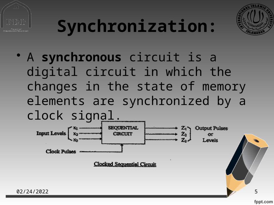
Synchronization:• A synchronous circuit is a digital circuit in
which the changes in the state of memory elements are synchronized by a clock signal.
05/02/2023 6
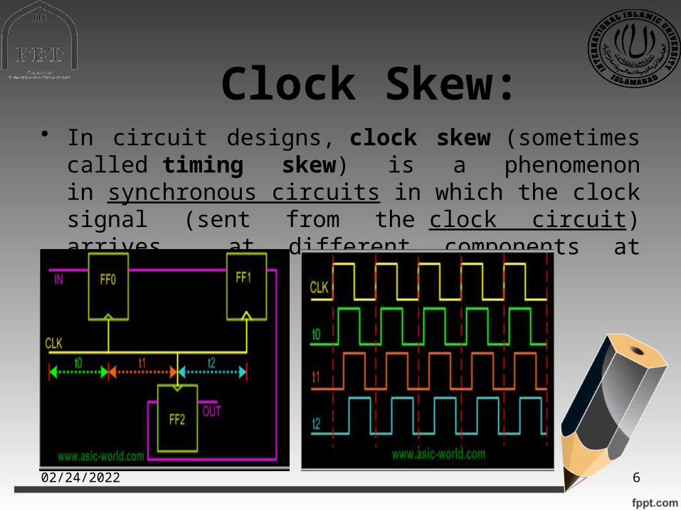
Clock Skew:• In circuit designs, clock skew (sometimes called timing
skew) is a phenomenon in synchronous circuits in which the clock signal (sent from the clock circuit) arrives at different components at different times.
05/02/2023 7
Clock Skew: The spatial variation in arrival time of a clock
transition on an integrated circuit is commonly referred to as clock skew.
Clock skew is caused by static path-length mismatches in the clock load and by definition skew is constant from cycle to cycle.
That is, if in one cycle CLK2 lagged CLK1 byδ, then on the next cycle it will lag it by the same amount.
05/02/2023 8
Types of skew:There are three types of clock skew:1. Positive skew: It occurs when the transmitting register receives the
clock tick earlier than the receiving register (δ>0).2. Negative skew: Negative skew occurs when the receiving register gets
the clock tick earlier than the sending register(δ<0).3. Zero clock skew: Zero clock skew refers to the arrival of the clock tick simultaneously at transmitting and receiving register.
05/02/2023 9
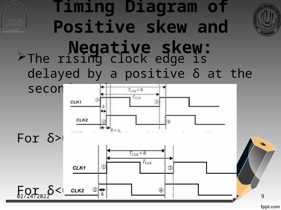
Timing Diagram of Positive skew and Negative skew:
The rising clock edge is delayed by a positive δ at the second register.
For δ>0:
For δ<0:
05/02/2023 10
Clock Distribution:• On a small chip, the clock distribution network is just a
wire .• And possibly an inverter for second clock.• On practical chips, the RC delay of the wire resistance
and gate load is very long .• Variations in this delay cause clock to get to different
elements at different times .• This is called clock skew .• Most chips use repeaters to buffer the clock and equalize the delay .• Reduces but doesn’t eliminate skew.
05/02/2023 11
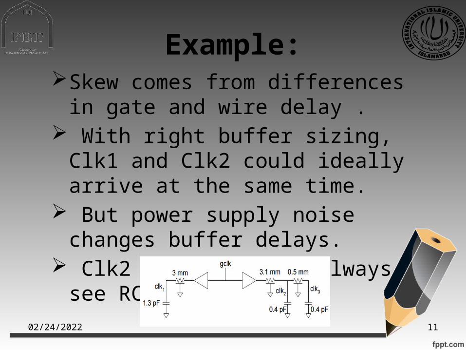
Example:Skew comes from differences in gate
and wire delay . With right buffer sizing, Clk1 and Clk2
could ideally arrive at the same time. But power supply noise changes buffer
delays. Clk2 and Clk3 will always see RC
skew.
05/02/2023 12
Solutions: Reduce clock skew: Careful clock distribution network design . Plenty of metal wiring resources . Tolerate clock skew : Choose circuit structures insensitive to skew.

05/02/2023 13
Clock Jitter:
Temporal variation of the clock period at a given point .
Clock period can reduce or expand on a cycle-by-cycle basis and is often specified at a given point on the chip.
Jitter directly impacts the performance of a sequential system.

05/02/2023 14
Clock Jitter:• The cycle-to-cycle jitter (T jitter) typically
refers to the time-varying deviations of a signal clock period relative to an ideal reference clock.

05/02/2023 15
Causes• Clock generator circuitry.• Noise.• Power supply variations.• Interference from nearby circuitry etc. Jitter is a contributing factor to the design margin specified for timing closure.Must reduce jitter in the clock network to
maximize performance.

05/02/2023 16
JITTER TYPES:Based on how it is measured in a system,
Jitter is of following types:
• Period jitter.• Cycle to cycle jitter.• Phase jitter.
05/02/2023 17
Period jitter• Deviation in cycle time of a clock signal w.r.t the
ideal period over a number of randomly selected cycles(say 10K cycles).
• An average value of clock period deviation over the selected cycles(RMS value)
• Difference of Max and Min deviation within the selected group
05/02/2023 18
Cycle to cycle jitter.• C2C is the deviation in cycle of two
adjacent clock cycles over a random number of clock cycles. (say 10K).
• This is typically reported as a peak value within the random group.
• This is used to determine the high frequency jitter.
05/02/2023 19
Phase jitter:• It is the frequency domain representation of rapid, short-
term, random fluctuations in the phase of a waveform. • This can be translated to jitter values for use in digital
design.

05/02/2023 20
Effects of jitter:• Jitter affects the clock delay of the circuit and the time• The clock is available at sync points, setup and hold of
the path elements are affected by it.• Performance or functional issues for the chip.• So it is necessary that the designer knows the jitter
values of the clock signal and account for it while analyzing timing.
05/02/2023 21
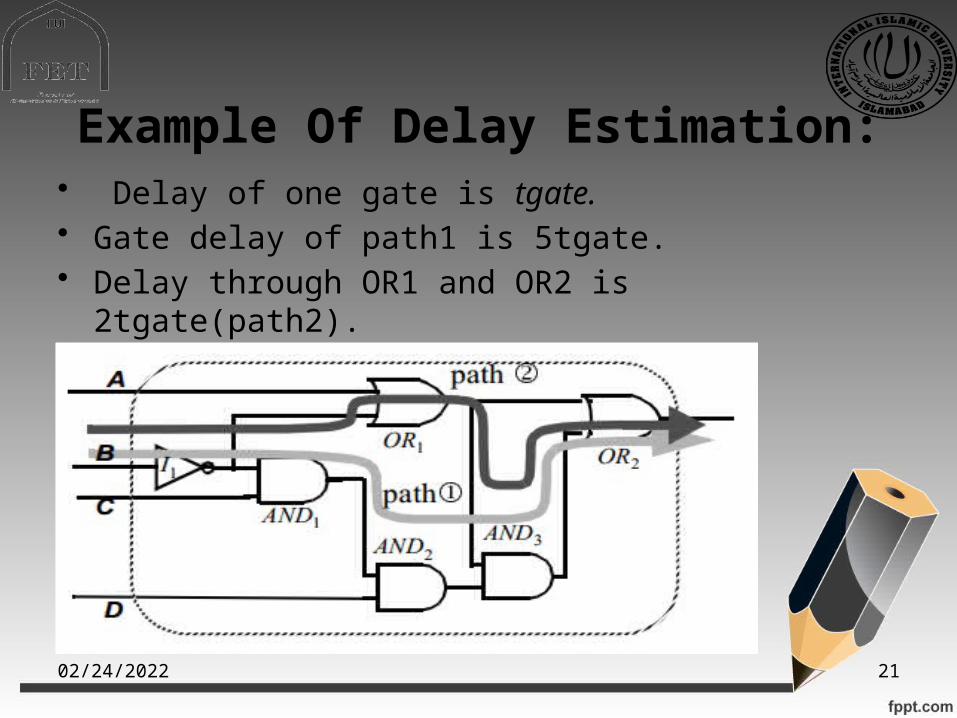
Example Of Delay Estimation:• Delay of one gate is tgate.• Gate delay of path1 is 5tgate.• Delay through OR1 and OR2 is 2tgate(path2).

05/02/2023 22
Errors Of Clock Sources:
Errors can be divided into: Systematic: Systematic errors are nominally identical from chip to
chip, and are typically predictable. Systematic errors can be deduced from measurements
over a set of chips. Random: Random errors are due to manufacturing variations . Are difficult to model and eliminate.
05/02/2023 23
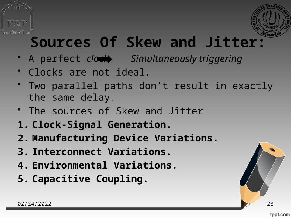
Sources Of Skew and Jitter:• A perfect clock Simultaneously triggering• Clocks are not ideal.• Two parallel paths don’t result in exactly the same delay.• The sources of Skew and Jitter1. Clock-Signal Generation.2. Manufacturing Device Variations.3. Interconnect Variations.4. Environmental Variations.5. Capacitive Coupling.
05/02/2023 24
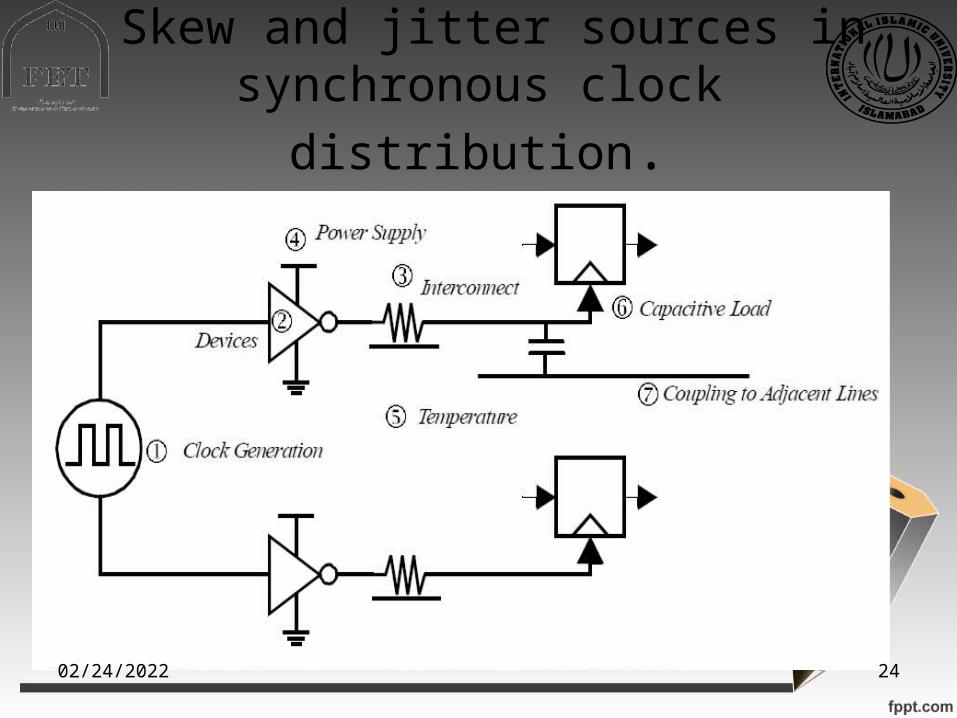
Skew and jitter sources in synchronous clock distribution.
05/02/2023 25
` Sources of Skew and Jitter1. Clock-Signal Generation:• The generation of the clock signal itself causes jitter.• Low-frequency reference clock high-frequency• VCO2 .Manufacturing Device Variations:• There are many sources of variations including Oxide variations (that affects the gain and threshold). Dopant variations.(depth of junction) Lateral dimension (width and length) variations.
05/02/2023 26
Sources of Skew and Jitter Contd.
• Temperature (Power Dissipation)• Power supply
3. Interconnect Variations:
Inter-layer Dielectric (ILD) thickness variations.
4. Environmental Variations
Temperature gradients across the chip is a result of variations in power dissipation across the die.5. Capacitive Coupling:• Coupling between the clock wire and adjacent signal results in timing
uncertainty.• Another major source of clock uncertainty is variation
in the gate capacitance related to the sequential elements.
05/02/2023 27
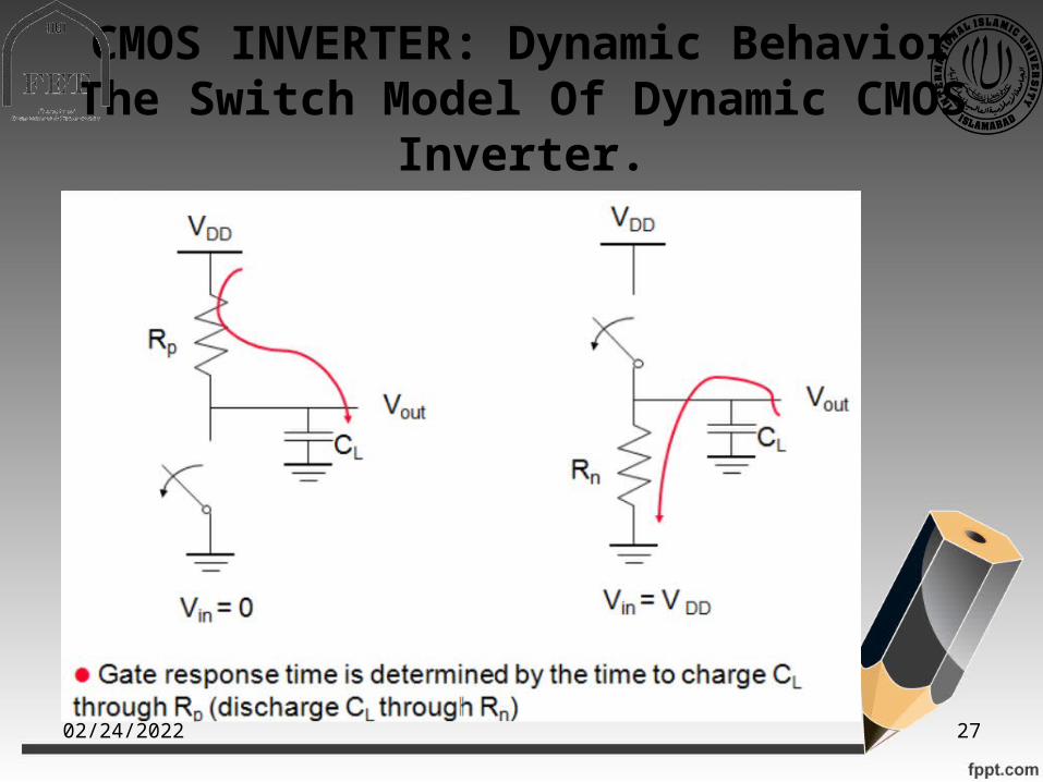
CMOS INVERTER: Dynamic BehaviorThe Switch Model Of Dynamic CMOS
Inverter.

05/02/2023 28
CMOS INVERTER: Dynamic BehaviorParasitic Capacitances of CMOS inverter
05/02/2023 29
Gate-Drain Capacitance Cgd12:
• The only contributions to Cgd12 are the overlap capacitances of both M1 and M2.
• This floating gate-drain capacitor be replaced by a capacitance-to-ground, so-called Miller effect .
• During a low-high or high-low transition, the terminals of the gatedrain capacitor are moving in opposite directions. .
• The voltage change over the floating capacitor is hence twice the actual output voltage swing.
05/02/2023 30
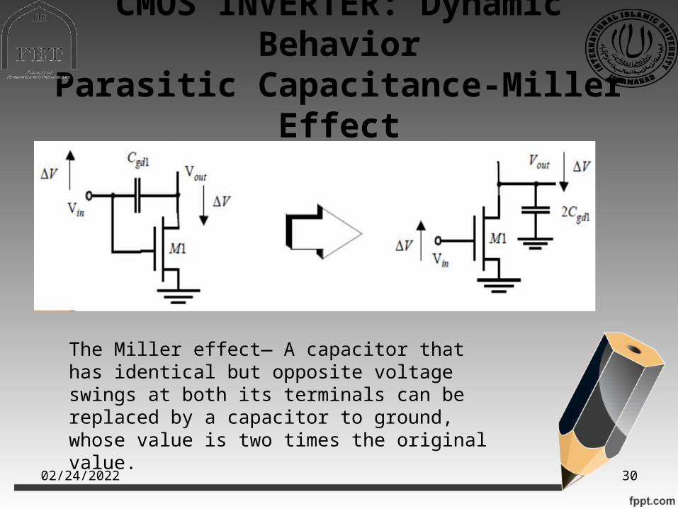
CMOS INVERTER: Dynamic Behavior
Parasitic Capacitance-Miller Effect
The Miller effect— A capacitor that has identical but opposite voltage swings at both its terminals can be replaced by a capacitor to ground, whose value is two times the original value.
05/02/2023 31
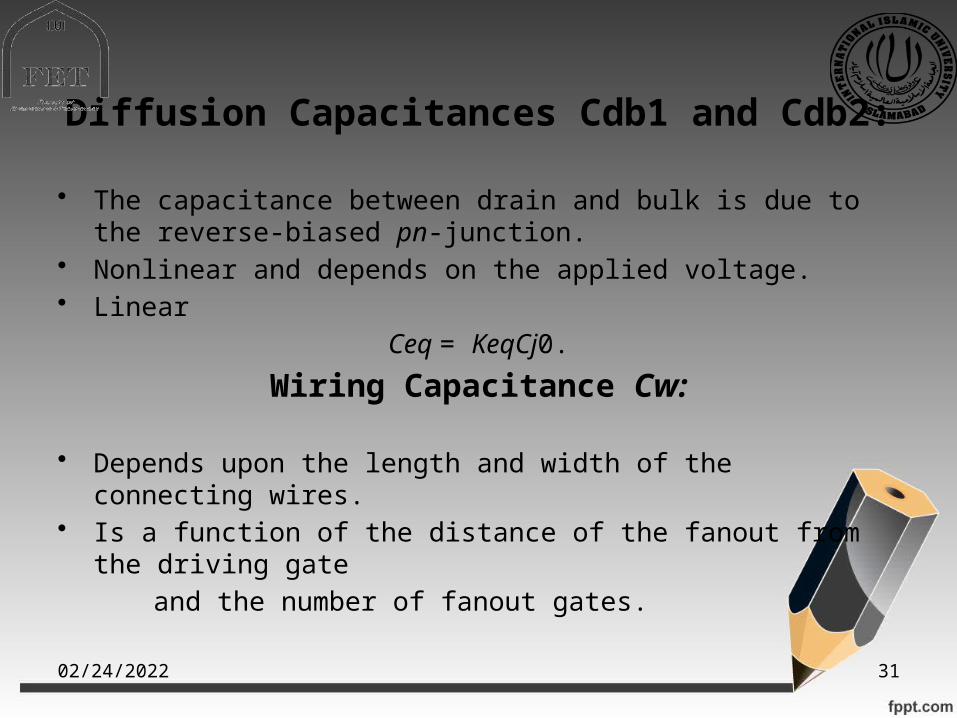
Diffusion Capacitances Cdb1 and Cdb2:
• The capacitance between drain and bulk is due to the reverse-biased pn-junction.
• Nonlinear and depends on the applied voltage.• Linear
Ceq = KeqCj0.
Wiring Capacitance Cw:
• Depends upon the length and width of the connecting wires.• Is a function of the distance of the fanout from the driving gate and the number of fanout gates.
05/02/2023 32
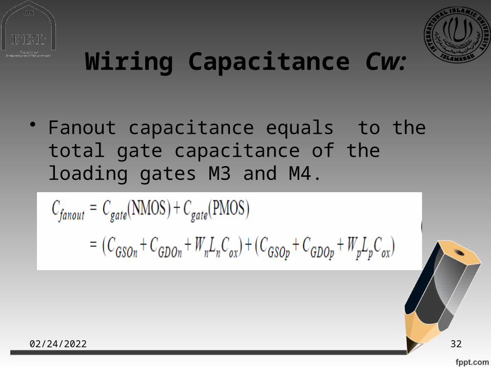
Wiring Capacitance Cw:
• Fanout capacitance equals to the total gate capacitance of the loading gates M3 and M4.
05/02/2023 33
Solutions • Shielding clock wires from adjacent signal wires to avoid
noise• Avoid too much parallel routing of metals• Decoupling capacitors are used to avoid power supply
variation in jitter• Use local clock in place of routed clock to avoid skew• Clock buffer delay can be reduced by feedback circuits

05/02/2023 34
Any Questions?