reducing signal transmission loss by low surface … signal transmission loss by low surface...
TRANSCRIPT
Reducing signal transmission loss
by low surface roughness
Taka-aki Okubo1), Toshio sudo1),
Toshihiro Hosoi2), Hiroaki Tsuyoshi2), and Fujio Kuwako2)
1)Shibaura-institute of Technology 2)Mitsui- Mining & Smelting Co., Ltd.

Agenda
1. Introduction and research purpose
2. Signal transmission loss
3. Configuration of the evaluation board
4. Measurement and simulated results
5. Loss and surface roughness of copper foil
6. Summary

Agenda
1. Introduction and research purpose
2. Signal transmission loss
3. Configuration of the evaluation board
4. Measurement and simulated results
5. Loss and surface roughness of copper foil
6. Summary

Introduction and Research purpose
Introduction
1. Higher-speed signal transmission is strongly required on a printed
circuit board to handle massive data in electronic systems.
2. So, signal transmission loss of copper wiring on a printed circuit
board has been studied.
3. First, total signal loss was divided into dielectric loss and
conductor loss quantitatively based on electromagnetic theory.
4. In particular, the scattering loss due to surface roughness of copper
foil has been examined in detail.
Research purpose
To demonstrate the usefulness of the copper foil with low surface
roughness for higher-speed signal transmission.

Agenda
1. Introduction and research purpose
2. Signal transmission loss
3. Configuration of the evaluation board
4. Measurement and simulated results
5. Loss and surface roughness of copper foil
6. Summary

Signal transmission loss (1)
Signal transmission loss on printed circuit boards can be classified into
conductor loss and dielectric loss.
Conductor loss can be classified into scattering loss caused by surface
roughness and the skin effect loss.
On the other hand, dielectric loss is due to dielectric loss tangent and relative
permittivity.

Signal transmission loss (2)
Total loss Total signal transmission loss can be expressed by two loss factors.
Where,𝑳𝒐𝒔𝒔𝑫is dielectric loss, 𝑳𝒐𝒔𝒔𝑪is conductor loss.
Conductor loss Conductor loss is represented by the following equation.
Where,𝑳𝒐𝒔𝒔𝑪 is conductor loss, 𝑳𝒐𝒔𝒔𝑲 is skin effect loss and 𝑳𝒐𝒔𝒔𝑺is scattering loss.
Conductor loss is composed of scattering loss and skin effect loss.
Loss = 𝑳𝒐𝒔𝒔𝑪 + 𝑳𝒐𝒔𝒔𝑫
𝑳𝒐𝒔𝒔𝑪 = 𝑳𝒐𝒔𝒔𝑲 + 𝑳𝒐𝒔𝒔𝑺

Frequency dependency of skin depth
in copper conductor
Skin depth δ is defined by the distance where the current amplitude becomes 1/e
times of the surface current amplitude in the conductor.
In the frequency of 1GHz, the skin depth is about 2.1 μm.
Current distribution is concentrated at the surface, or the edge of the conductor at
high frequencies. This is the skin effect.

Skin effect loss
Skin effect Skin effect is represented by following equation.
Where, 𝜹 is skin depth, 𝝎 is angular frequency, 𝝁is permeability, 𝝈is conductivity of copper and 𝒇is frequency.
Skin effect δ is inversely proportional of the square root of the frequency.
Skin effect loss The loss due to skin effect is represented by following equation.
Where, w is wiring width of copper.
Skin effect loss is proportional to the square root of frequency.
𝜹 =𝟐
𝝎𝝁𝝈 =
𝟏
𝝅𝒇𝝁𝝈
𝑳𝒐𝒔𝒔𝑯 =𝟐. 𝟐𝟔 × 𝟏𝟎−𝟖 × 𝒇
𝒘 [dB/m]

Cross-section of copper conductor
Usually, the surface of the conductor in printed circuit boards is intentionally
roughened to enhance the adhesion to the prepreg.
Typical surface roughness of the copper foil commonly used in printed circuit
boards was 6 μm.
This is a value greater than 2.1 μm of the skin depth at 1GHz.
Because skin depth becomes smaller than surface roughness at high frequency,
the scattering loss becomes prominent.
Surface roughness

Dielectric loss
Dielectric loss
Dielectric loss is represented by the following equation.
Where, 𝜺𝜸is relative permittivity,𝒕𝒂𝒏 𝜹is dielectric loss tangent and 𝒇 is frequency.
Dielectric loss is proportional to the frequency.
Dielectric loss is affected by dielectric loss tangent and relative permittivity of the
dielectric.
𝑳𝒐𝒔𝒔𝑫 = 𝟗𝟎. 𝟗 𝜺𝜸 × 𝒕𝒂𝒏 𝜹 × 𝒇

Agenda
1. Introduction and research purpose
2. Signal transmission loss
3. Configuration of the evaluation board
4. Measurement and simulated results
5. Loss and surface roughness of copper foil
6. Summary

Configuration of the evaluation board
The evaluation boards included into the four types of transmission line structures.
They are microstrip and strip structures for single-ended transmission line and there are
those structures for differential transmission line.
The dotted red lines on the conductors show mat faces of copper foils.
The characteristic impedance for single-ended line was configured to 50 ohms and the
differential impedance for differential line was configured to 100 ohms.
Single-ended Differential

Properties of dielectric materials
The evaluation boards have been provided with three types of the dielectric materials.
They are low dielectric material G1, G2 and commonly used dielectric material, FR-4.
This table shows relative permittivity and dielectric loss tangent of each materials.

Agenda
1. Introduction and research purpose
2. Signal transmission loss
3. Configuration of the evaluation board
4. Measurement and simulated results
5. Loss and surface roughness of copper foil
6. Summary
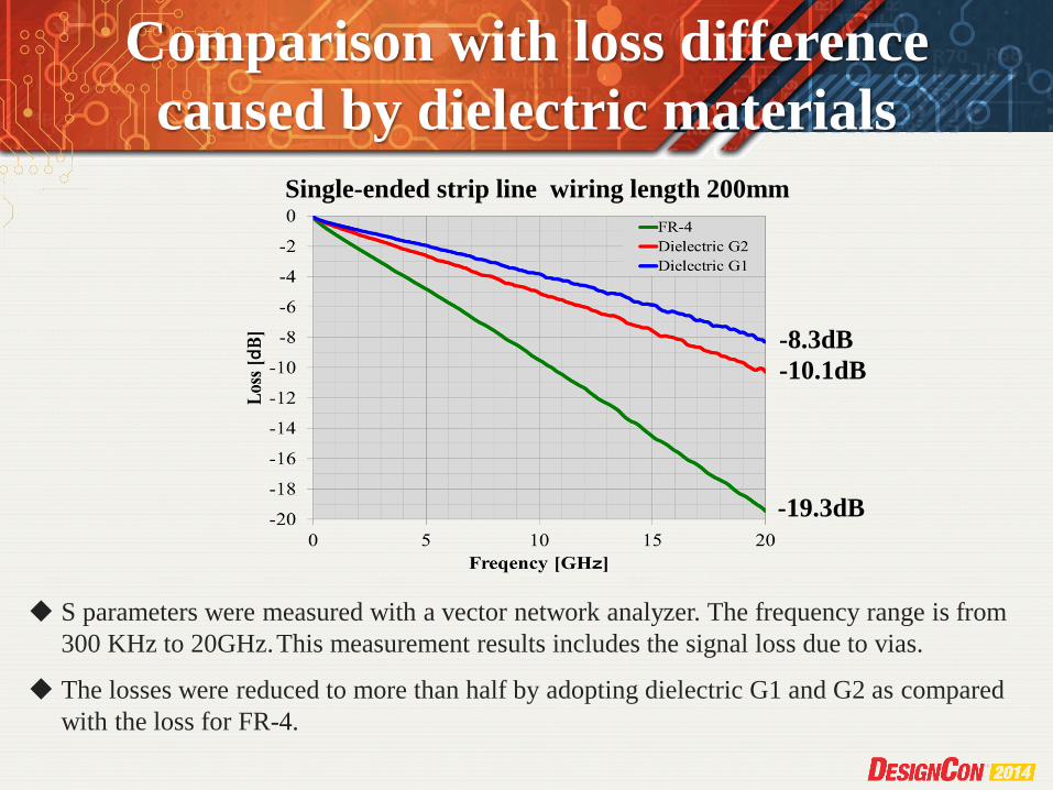
Comparison with loss difference
caused by dielectric materials
S parameters were measured with a vector network analyzer. The frequency range is from
300 KHz to 20GHz. This measurement results includes the signal loss due to vias.
The losses were reduced to more than half by adopting dielectric G1 and G2 as compared
with the loss for FR-4.
Single-ended strip line wiring length 200mm
-8.3dB
-10.1dB
-19.3dB

How to deduce the loss due to vias?
This figure shows the losses for three wiring lengths at 1GHz.
The red plots indicate the measured losses in each wiring length and the blue line is the
regression line of them.
The intercept of the blue line shows the via loss value. The value of the via loss was -
0.00679dB at 1GHz.

Deduction of via loss from measurement
This figure shows the deduced via loss from 1GHz to 20 GHz.
The red line shows plots of loss due to vias in each frequency. The blue line shows
approximated curved line for the red line.
The deduced via loss was approximately -2.8 dB at 20 GHz.
Plot of the loss
The approximate

Calibrated S21 without via loss
This figure shows calibrated S21 that does not include the loss due to vias.
In case of dielectric G1, the loss value was about -5.4 dB at 20 GHz.
On the other hand, the loss value for FR-4 was about -16.6 dB at 20 GHz.
-16.6dB
-7.4dB
-5.4dB
Single-ended strip line wiring length 200mm

Simulated S21 by HFSS model
The signal loss was analyzed with 3D electromagnetic solver, HFSS.
This figure shows the analysis model of wiring on a printed circuit board.
The model was single-ended strip structure and wiring length was 200mm.

HFSS model without via
This figure shows a port of HFSS model without via.
The ports were set to wave port. This wave port is the ideal port.
Wave port
Air Ground
Wiring
Dielectric
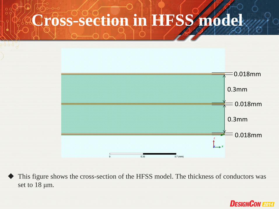
Cross-section in HFSS model
This figure shows the cross-section of the HFSS model. The thickness of conductors was
set to 18 μm.
0.018mm
0.018mm
0.018mm
0.3mm
0.3mm

Plane view of wiring trace in HFSS
This figure shows plane view of wiring trace in HFSS model.
The distance between the edge of the wiring and the wiring model was 3mm.
3 mm
Wiring width

Comparison with measured S21 and HFSS result
The measured S21 includes the scattering loss caused by surface roughness of the conductor.
On the other hand, simulated S21 with HFSS does not include the scattering loss due to surface
roughness. The simulated model by HFSS was assumed to be completely smooth surface.
Then, the difference of S21 between measured S21 and HFSS result shows the amount of scattering
loss, which was estimated to be approximately 1.5 dB at 20 GHz.
Structure : Single-ended strip, Wiring length: 200mm, Dielectric : FR-4
RTF

How to decompose the total loss
into loss factors?
◆ The entire loss is represented by following equation.
where, A and B are proportional constant of each loss.
The amount of each loss factor can be obtained by determining the values of A and B.
The following equation is the result by dividing the entire loss with the square root of the
frequency.
The values of the constant A and B were obtained from S21 dividing the square root of the
frequency. The constant A is the slope and the constant B is the intercept of the graph.
𝑳𝒐𝒔𝒔 = 𝑳𝒐𝒔𝒔𝑫 + 𝑳𝒐𝒔𝒔𝑪 = 𝑨𝒇 + 𝑩 𝒇
𝑳𝒐𝒔𝒔
𝒇= 𝑨 𝒇 + 𝑩

S21/ 𝒇and regression line
The blue line shows plots of the S21 divided by the square root of the frequency for FR-4
and red line shows the regression line of that.
The constant A and B were obtained from the regression line.
A B
S21/√ f
Regression line

This figure shows the decomposed each loss factors of simulated result with HFSS.
The orange line indicates the conductor loss due to only skin effect.
On the other hand, the green line shows the dielectric loss.
Total loss and loss factors for FR-4
-2.3dB (Skin effect loss)
-12.9dB (Dielectric loss)
-15.0dB ( Analysis result )

Total loss and decomposed loss factors
for FR-4
The red trace shows the measured result for foil MLS-G(RTF).
The sum of two loss factors decomposed from measured result was well coincident
with the simulated result by HFSS.
The estimated value of conductor loss was about 3.6 dB at 20 GHz. It corresponds
to about 22% for total loss at 20 GHz.
-2.3dB (Skin effect loss)
-12.9dB (Dielectric loss)
-16.5dB ( Measurement result )
3.6dB = 22%

Total loss and decomposed loss factors
for dielectric G1
This figure shows the decomposed each loss factors in case of dielectric G1.
Each loss factor was decomposed from total loss which agreed well with simulated result.
In comparison with FR-4, the dielectric loss was reduced considerably, then the percentage
of the skin effect loss was relatively increased.
-2.2dB (Dielectric loss)
-4.8dB (HFSS result)
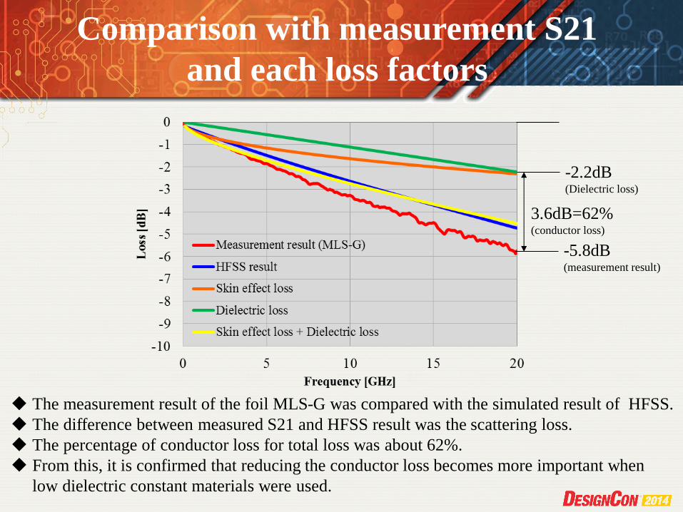
Comparison with measurement S21
and each loss factors
The measurement result of the foil MLS-G was compared with the simulated result of HFSS.
The difference between measured S21 and HFSS result was the scattering loss.
The percentage of conductor loss for total loss was about 62%.
From this, it is confirmed that reducing the conductor loss becomes more important when
low dielectric constant materials were used.
-5.8dB (measurement result)
-2.2dB (Dielectric loss)
3.6dB=62% (conductor loss)

Agenda
1. Introduction and research purpose
2. Signal transmission loss
3. Configuration of the evaluation board
4. Measurement and simulated results
5. Loss and surface roughness of copper foil
6. Summary

Surface roughnesses of copper foils
RTF(MLS-G) MWG-VSP
HS-VSP HS1-VSP
NP-VSP
RTF(MLS-G) MWG-VSP
HS-VSP HS1-VSP
NP-VSP
These figures show SEM image and
schematic image of each copper foil.
Large tangled Cu
Small tangled Cu
Large tangled Cu
Very small tangled Cu:
No tangled Cu (Primer was used instead of tangles.)
Resist side : Large waving
Resist side : small waving
Resist side : small waving
Resist side : small waving
Resist side : Little waving

Surface roughnesses on the mat face
[μ m]copper foil Laser microscope Zygo
RTF 2.49 3.13MWG-VSP 0.99 1.21HS-VSP 0.97 1.23HS1-VSP 1.06 0.99NP-VSP 1.25 1.15
[μ m]copper foil Laser microscope Zygo
RTF 3.95 4.21MWG-VSP 3.75 3.86HS-VSP 2.13 1.80HS1-VSP 1.42 1.09NP-VSP 0.19 0.29
Rz : average of ten points on the surface Rq : root-mean-square of roughnesses
Surface roughness of each copper foils were RTF > MWG-VSP > HS-VSP > NP-VSP.

Surface roughnesses on the shiny face
[μ m]copper foil Laser microscope Zygo
RTF 2.49 3.13MWG-VSP 0.99 1.21HS-VSP 0.97 1.23HS1-VSP 1.06 0.99NP-VSP 1.25 1.15
[μ m]copper foil Laser microscope Zygo
RTF 0.51 0.42MWG-VSP 0.18 0.16HS-VSP 0.18 0.17HS1-VSP 0.17 0.13NP-VSP 0.22 0.12
Rz : average of ten points on the surface Rq : root-mean-square of roughnesses
The surface roughnesses on the shiny face of each copper foils were
RTF>MWG-VSP≒HS-VSP≒HS1-VSP≒NP-VSP.

The loss difference due to surface
roughness of copper foils
When the foil MLS-G(RTF) was compared with the foil NP-VSP, the signal loss of the foil
NP-VSP was reduced by approximately 23.8% of the signal loss of the foil MLS-G.
This shows that the usage of copper foil with low surface roughness is effective to reduce
the scattering loss of the conductor.
1.4dB=23.8%
100% -4.49dB (NP-VSP)
-5.89dB (MLS-G)
NP-VSP
HS1-VSP
HS-VSP
MWG-VSP
MLS-G(RTF)

Relationships between signal loss
and surface roughness
This figure shows the relationship between loss and surface roughness of each
copper foils.
It was confirmed that as the roughness became smaller, the loss was decreased.

Summary
1) In this research, S parameters of various types of transmission lines structures on an
evaluation board were measured and simulated in detail. Furthermore, several types of
surface roughnesses of copper conductors have been examined.
2) First, purely total signal loss for the stripline structure has been obtained by deducting the
loss due to via structure. Next, the pure total loss has been decomposed into the conductor
loss due to skin effect and the dielectric loss along with HFSS model. Finally, the amount
of scattering loss due to surface roughness has been extracted.
3)Signal loss has been greatly reduced by adopting low dielectric constant material. It has
been confirmed that the signal loss of dielectric G1 was reduced by about 68% compared
with the signal loss of FR-4.
4) Low roughness copper foil has been found to be effective in reducing the overall loss when
low dielectric material is used as dielectric. When the foil A was compared with the foil D,
signal loss was reduced by about 1.4 dB, at 20 GHz. This corresponds to approximately
23.8% reduction in the conductor loss.

Thank you for listening.