signal transmission loss due to copper surface roughness ... · signal transmission loss due to...
TRANSCRIPT
Signal Transmission Loss due to Copper Surface Roughness in
High-Frequency Region
Elaine Liew, Mitsui Copper Foil Malaysia, Shah Alam Malaysia
Taka-aki Okubo, Toshio Sudo, Shibaura Institute of Technology, Tokyo Japan
Toshihiro Hosoi, Hiroaki Tsuyoshi, Fujio Kuwako, Mitsui Kinzoku Co., Ltd, Japan
Abstract
Higher-speed signal transmission is increasingly required on a printed circuit board to handle massive data in electronic
systems. So, signal transmission loss of copper wiring on a printed circuit board has been studied. First, total signal loss was
divided into dielectric loss and conductor loss quantitatively based on electromagnetic theory. In particular, the scattering loss
due to surface roughness of copper foil has been examined in detail and the usefulness of the copper foil with low surface
roughness has been demonstrated.
Introduction
Higher performance IT electronic systems are strongly required to handle huge amounts of data in a shorter time in recent
years. Transmission speed of the signals propagating inside the equipment has been increasing. Signal loss becomes
remarkable on a printed circuit board in the GHz frequency range. It causes many problems, such as rising edge degradation
of signals, or resulting higher bit error rate, and so on. Then, reducing the signal loss on a printed circuit board has become
more important. Therefore, in this study, measurement of S21 has been carried out by fabricating various evaluation boards
combining different copper foils with low roughness and low dielectric materials. And they were compared with the
transmission loss of the commonly used material, FR-4. In particular, the reduction effect of signal loss has been
demonstrated quantitatively by using copper foil with smooth surface roughness along with low dielectric loss material.
Signal transmission loss
Signal transmission loss on printed circuit boards can be classified into conductor loss due to the conductor and dielectric loss
due to the dielectric. Then, total signal transmission loss can be expressed by two loss factors.
(1)
Where, is dielectric loss and is conductor loss.
Dielectric loss is represented by the following equation (2).
(2)
where, relative permittivity, is dielectric loss tangent, and is frequency in GHz. Conductor loss can be divided
into scattering loss caused by surface roughness and the skin effect loss. Then, it is represented by the formula (3).
(3)
where, the loss due to skin effect, and is scattering loss. Current distribution is concentrated at the surface or
the edge of the conductor at high frequencies. Skin depth δ is an index representing skin effect. Skin depth δ is defined by the
distance where the current amplitude becomes 1/e times of the surface current amplitude in the conductor, and it is
represented by the formula (4).
(4)
As originally published in the IPC APEX EXPO Conference Proceedings.

where, is angular frequency, is permeability, and is conductivity of copper.
Figure 1 : Frequency dependency of skin depth for copper Figure 1 shows frequency dependency of the skin depth in copper conductor. The skin depth is approximately 2.1 μm at 1
GHz. Effective cross-section area of the conductor for the current flow becomes restricted at high frequencies. Therefore,
signal line impedance increases with the frequency. Signal loss due to skin effect is represented by the formula (5).
(5)
where, w is wiring width of conductor. Figure 2 shows a SEM image of cross-section of a printed circuit board. Usually, the
surface of the conductor in printed circuit boards is intentionally roughened to enhance the adhesion to the prepregs. Typical
surface roughness Rz of the copper foil commonly used in printed circuit board is 6 μm. This is a value greater than 2.1 μm
of the skin depth at 1 GHz. Here, Rz is a ten-point average roughness of the surface. Because skin depth becomes smaller
than surface roughness at high frequency, the scattering loss becomes prominent[1][2][4][5].
Figure 2 : Surface roughness of copper conductor
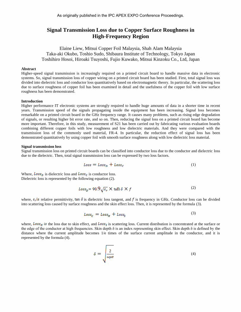
Configuration of the evaluation board
In order to investigate the relationship between the scattering loss and surface roughness of the conductor, various evaluation
boards were fabricated by different surface roughness of copper foils. Evaluation boards were made of four conductive layers
as shown Figure 3. In order to observe the difference in the transmission line structures, four types of transmission lines were
designed in the board. They were single-ended microstrip line and strip line, and differential microstrip line and strip line.
The characteristic impedance Zo for the single-ended transmission line was designed to 50 ohms, differential impedance was
designed to 100 ohms. Moreover, three kinds of dielectric materials were examined. They were dielectric material G1
(Dk=3.7, Df=0.002), dielectric G2 (Dk=3.8, Df=0.005), and commonly used dielectric material, FR-4 (Dk=4.4, Df=0.02).
Former two materials were low dielectric materials.
Figure 3 : Cross-section with 4 types of transmission lines
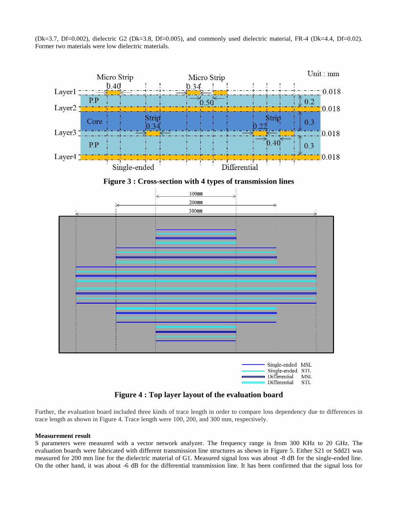
Figure 4 : Top layer layout of the evaluation board
Further, the evaluation board included three kinds of trace length in order to compare loss dependency due to differences in
trace length as shown in Figure 4. Trace length were 100, 200, and 300 mm, respectively.
Measurement result
S parameters were measured with a vector network analyzer. The frequency range is from 300 KHz to 20 GHz. The
evaluation boards were fabricated with different transmission line structures as shown in Figure 5. Either S21 or Sdd21 was
measured for 200 mm line for the dielectric material of G1. Measured signal loss was about -8 dB for the single-ended line.
On the other hand, it was about -6 dB for the differential transmission line. It has been confirmed that the signal loss for

differential transmission line is lower than the loss for single-ended transmission line. From this, it can be said that the
differential transmission line is also useful to reduce the losses in high-speed signal transmission[1][2].
Also, evaluation boards were fabricated with different materials as shown in Figure 6. Measured total signal loss was about -
19 dB for FR-4. On the other hand, it was about -10dB for the dielectric G2, and about -8 dB for the dielectric G1. The loss
of dielectric G1was reduced by 68% compared with FR-4. It has been confirmed that the use of low dielectric constant
material is necessary for high speed transmission.
Figure 4 : Comparison of the signal losses of FR4 for the four different transmission structures
Figure 5 : Comparison of measured signal losses due to the difference of dielectric material
Decomposition of total loss into loss factors of copper and dielectric
Measured total signal losses for low dielectric constant materials were dramatically reduced, then the ratio of dielectric loss
among total signal loss was decreased, and the ratio occupied by the conductor loss was relatively increased.
Next, the ratio of conductor loss and dielectric loss among the overall loss was examined. Total attenuation constant can be
represented by the formula (6). As shown in the formula, the dielectric loss is proportional to the frequency, while the
conductor loss is proportional to the square root of the frequency.
(6)
In addition, equation (7) can be obtained by dividing the equation (6) by the square root of the frequency.
(7)
Constants A and B are proportional coefficients of each loss. These values of constants A and B can be obtained by using the
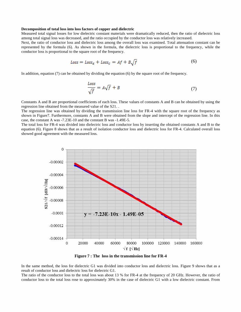
regression line obtained from the measured value of the S21. .
The regression line was obtained by dividing the transmission line loss for FR-4 with the square root of the frequency as
shown in Figure7. Furthermore, constants A and B were obtained from the slope and intercept of the regression line. In this
case, the constant A was -7.23E-10 and the constant B was -1.49E-5.
The total loss for FR-4 was divided into dielectric loss and conductor loss by inserting the obtained constants A and B to the
equation (6). Figure 8 shows that as a result of isolation conductor loss and dielectric loss for FR-4. Calculated overall loss
showed good agreement with the measured loss.
Figure 7 : The loss in the transmission line for FR-4
In the same method, the loss for dielectric G1 was divided into conductor loss and dielectric loss. Figure 9 shows that as a
result of conductor loss and dielectric loss for dielectric G1.
The ratio of the conductor loss to the total loss was about 13 % for FR-4 at the frequency of 20 GHz. However, the ratio of
conductor loss to the total loss rose to approximately 30% in the case of dielectric G1 with a low dielectric constant. From
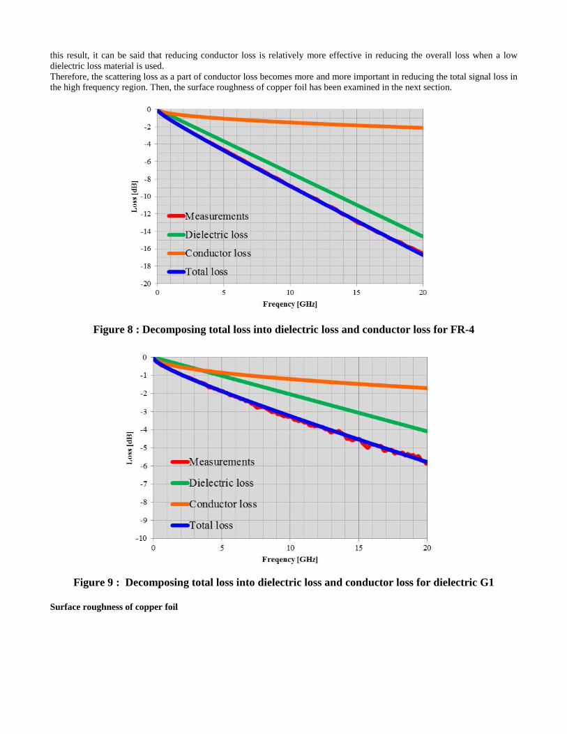
this result, it can be said that reducing conductor loss is relatively more effective in reducing the overall loss when a low
dielectric loss material is used.
Therefore, the scattering loss as a part of conductor loss becomes more and more important in reducing the total signal loss in
the high frequency region. Then, the surface roughness of copper foil has been examined in the next section.
Figure 8 : Decomposing total loss into dielectric loss and conductor loss for FR-4
Figure 9 : Decomposing total loss into dielectric loss and conductor loss for dielectric G1
Surface roughness of copper foil
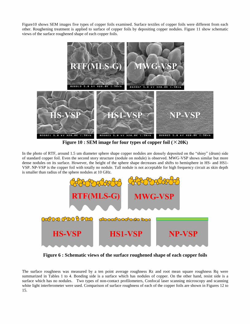
Figure10 shows SEM images five types of copper foils examined. Surface textiles of copper foils were different from each
other. Roughening treatment is applied to surface of copper foils by depositing copper nodules. Figure 11 show schematic
views of the surface roughened shape of each copper foils.
Figure 10 : SEM image for four types of copper foil (×20K)
In the photo of RTF, around 1.5 um diameter sphere shape copper nodules are densely deposited on the “shiny” (drum) side
of standard copper foil. Even the second story structure (nodule on nodule) is observed. MWG-VSP shows similar but more
dense nodules on its surface. However, the height of the sphere shape decreases and shifts to hemisphere in HS- and HS1-
VSP. NP-VSP is the copper foil with totally no nodule. Tall nodule is not acceptable for high frequency circuit as skin depth
is smaller than radius of the sphere nodules at 10 GHz.
Figure 6 : Schematic views of the surface roughened shape of each copper foils
The surface roughness was measured by a ten point average roughness Rz and root mean square roughness Rq were
summarized in Tables 1 to 4. Bonding side is a surface which has nodules of copper. On the other hand, resist side is a
surface which has no nodules. Two types of non-contact profilometers, Confocal laser scanning microscopy and scanning
white light interferometer were used. Comparison of surface roughness of each of the copper foils are shown in Figures 12 to
15.
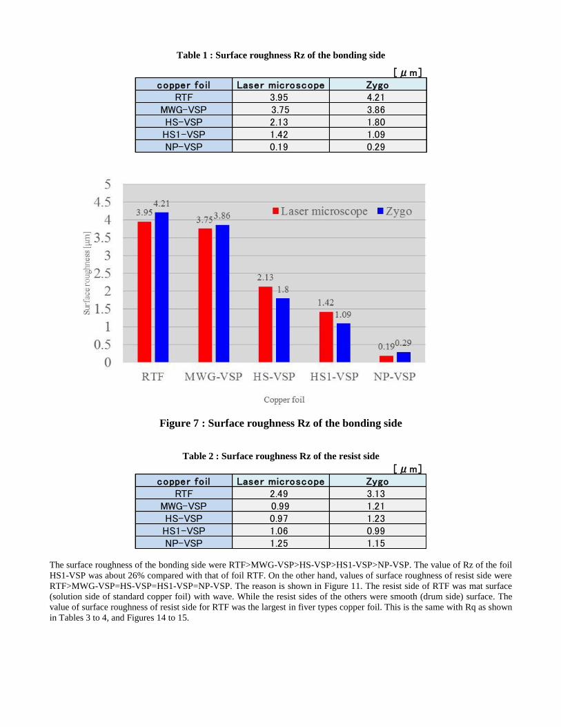
Table 1 : Surface roughness Rz of the bonding side
Figure 7 : Surface roughness Rz of the bonding side
Table 2 : Surface roughness Rz of the resist side
[μm]copper foil Laser microscope Zygo
RTF 2.49 3.13MWG-VSP 0.99 1.21HS-VSP 0.97 1.23HS1-VSP 1.06 0.99NP-VSP 1.25 1.15
The surface roughness of the bonding side were RTF>MWG-VSP>HS-VSP>HS1-VSP>NP-VSP. The value of Rz of the foil
HS1-VSP was about 26% compared with that of foil RTF. On the other hand, values of surface roughness of resist side were
RTF>MWG-VSP=HS-VSP=HS1-VSP=NP-VSP. The reason is shown in Figure 11. The resist side of RTF was mat surface
(solution side of standard copper foil) with wave. While the resist sides of the others were smooth (drum side) surface. The
value of surface roughness of resist side for RTF was the largest in fiver types copper foil. This is the same with Rq as shown
in Tables 3 to 4, and Figures 14 to 15.
[μm]copper foil Laser microscope Zygo
RTF 3.95 4.21MWG-VSP 3.75 3.86HS-VSP 2.13 1.80HS1-VSP 1.42 1.09NP-VSP 0.19 0.29
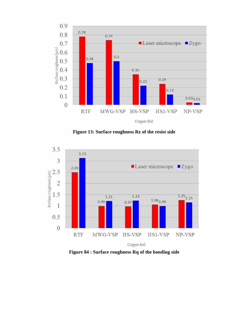
Figure 13: Surface roughness Rz of the resist side
Figure 84 : Surface roughness Rq of the bonding side
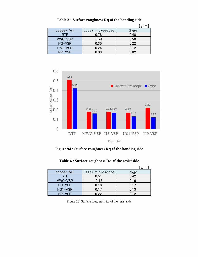
Table 3 : Surface roughness Rq of the bonding side
Figure 94 : Surface roughness Rq of the bonding side
Table 4 : Surface roughness Rq of the resist side
Figure 10: Surface roughness Rq of the resist side
[μm]copper foil Laser microscope Zygo
RTF 0.78 0.48MWG-VSP 0.74 0.50HS-VSP 0.35 0.22HS1-VSP 0.24 0.12NP-VSP 0.03 0.02
[μm]copper foil Laser microscope Zygo
RTF 0.51 0.42MWG-VSP 0.18 0.16HS-VSP 0.18 0.17HS1-VSP 0.17 0.13NP-VSP 0.22 0.12
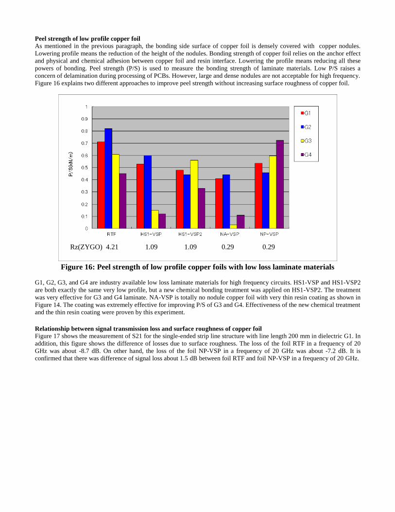
Peel strength of low profile copper foil As mentioned in the previous paragraph, the bonding side surface of copper foil is densely covered with copper nodules.
Lowering profile means the reduction of the height of the nodules. Bonding strength of copper foil relies on the anchor effect
and physical and chemical adhesion between copper foil and resin interface. Lowering the profile means reducing all these
powers of bonding. Peel strength (P/S) is used to measure the bonding strength of laminate materials. Low P/S raises a
concern of delamination during processing of PCBs. However, large and dense nodules are not acceptable for high frequency.
Figure 16 explains two different approaches to improve peel strength without increasing surface roughness of copper foil.
Figure 16: Peel strength of low profile copper foils with low loss laminate materials
G1, G2, G3, and G4 are industry available low loss laminate materials for high frequency circuits. HS1-VSP and HS1-VSP2
are both exactly the same very low profile, but a new chemical bonding treatment was applied on HS1-VSP2. The treatment
was very effective for G3 and G4 laminate. NA-VSP is totally no nodule copper foil with very thin resin coating as shown in
Figure 14. The coating was extremely effective for improving P/S of G3 and G4. Effectiveness of the new chemical treatment
and the thin resin coating were proven by this experiment. Relationship between signal transmission loss and surface roughness of copper foil
Figure 17 shows the measurement of S21 for the single-ended strip line structure with line length 200 mm in dielectric G1. In
addition, this figure shows the difference of losses due to surface roughness. The loss of the foil RTF in a frequency of 20
GHz was about -8.7 dB. On other hand, the loss of the foil NP-VSP in a frequency of 20 GHz was about -7.2 dB. It is
confirmed that there was difference of signal loss about 1.5 dB between foil RTF and foil NP-VSP in a frequency of 20 GHz.
Rz(ZYGO) 4.21 1.09 1.09 0.29 0.29
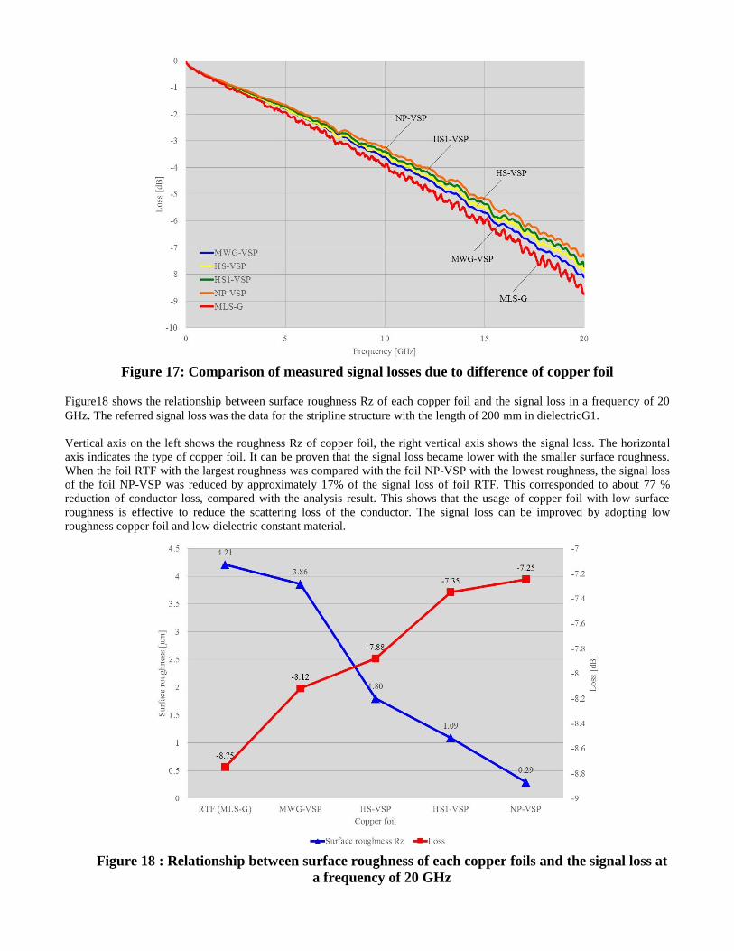
Figure 17: Comparison of measured signal losses due to difference of copper foil
Figure18 shows the relationship between surface roughness Rz of each copper foil and the signal loss in a frequency of 20
GHz. The referred signal loss was the data for the stripline structure with the length of 200 mm in dielectricG1.
Vertical axis on the left shows the roughness Rz of copper foil, the right vertical axis shows the signal loss. The horizontal
axis indicates the type of copper foil. It can be proven that the signal loss became lower with the smaller surface roughness.
When the foil RTF with the largest roughness was compared with the foil NP-VSP with the lowest roughness, the signal loss
of the foil NP-VSP was reduced by approximately 17% of the signal loss of foil RTF. This corresponded to about 77 %
reduction of conductor loss, compared with the analysis result. This shows that the usage of copper foil with low surface
roughness is effective to reduce the scattering loss of the conductor. The signal loss can be improved by adopting low
roughness copper foil and low dielectric constant material.
Figure 18 : Relationship between surface roughness of each copper foils and the signal loss at
a frequency of 20 GHz

Summary
In this research, S parameters of various types of transmission line structures on an evaluation board were measured and
analyzed in detail.
It was confirmed that reduction of signal loss for differential transmission line was greater than that for single-ended
transmission line. From this, it was shown that differential transmission line is useful for the reduction of losses in high-
speed signal transmission.
Signal loss has been greatly reduced by adopting low dielectric constant material. It has been confirmed that the signal
loss of dielectric G1 was reduced by about 68% compared with the signal loss of FR-4.
When using the low dielectric constant materials instead of FR-4, the ratio of the conductor loss against the entire loss
increases. The ratio of conductor loss for FR-4 was 13% of the total signal loss, but the conductor loss in dielectric G1
will increase to 30% among the overall loss.
If low dielectric material is used as dielectric, low roughness copper foil is effective in reducing the overall loss. Low
roughness copper foil was found to reduce by 73% of the scattering loss compared with commonly used surface
roughness of copper foil.
The chemical treatment on very low profile and the thin resin coating on no nodule copper foil are both very effective to
improve bond strength of laminates.
References
[1] S. Hinaga, M. Y. Koledintseva, P. K. R. Anmula, J. L. Drewniak, “Effect of Conductor Surface Roughness upon
Measured Loss and Extracted Values of PCB Laminate Material Dissipation Factor,” Proc. of IPC 2009.
[2] E. Bogatin, “Transmission technology of high-speed digital signal Signal Integrity Introduction” Pearson Education,
Inc. Chapter 9, pp.296-354, 2010.
[3] T. Suzuki, M. Ogihara, Y. Takada, T. Matsumoto, N. Senoku, “Study of transmission loss factors and influence of
surface roughness” MES2002 (12th Microelectronics Symposium), pp.443-446, October 2002.
[4] S. H. Hall & H. L. Heck, “Advanced Signal Integrity for High-speed digital circuit design” John Wiley & Sons, Inc.
Chapter 5 pp.189 -234, 2009.
[5] M. Y. Koledintseva, A. G. Razmadze, A. Y. Gafarov, Soumya De, J. L. Drewniak, and S. Hinaga, “PCB Conductor
Surface Roughness as a Layer with Effective Material Parameters,” Proc. of IEEE EMC Symposium, pp.138-143, 2012.