reduction of efficiency droop in ingan-based uv light ... · reduction of efficiency droop in...
TRANSCRIPT

Reduction of efficiency droop in InGaN-Based UV Light-Emitting Diodes with InAlGaN Barrier
Ching-Hsueh Chiu1, Po-Min Tu1, Jet-Rung Chang2, Wei-Ting Chang3, Hao-Chung Kuo1,*,
Chun-Yen Chang2 1Department of Photonics and Institute of Electro-Optical Engineering, National Chiao-Tung
University, Hsinchu 300, Taiwan 2Institute of Electronics, National Chiao-Tung University, Hsinchu 300, Taiwan.
3Department of Electro-Physics, National Chiao-Tung University, Hsinchu 300, Taiwan
TEL: +886-3-5712121#56354, Tai-wan* [email protected]
ABSTRACT
In this study, we fabricated and compared the performance of LEDs of InGaN-based UV MQWs active region with
ternary AlGaN and quaternary InAlGaN barrier layers. HRXRD and TEM measurements show the two barriers are
consistent with the lattice, and smooth morphology of quaternary InAlGaN layer can be observed in AFM. The
electroluminescence results indicate that the light performance of the InGaN-based UV LEDs can be enhanced
effectively when the conventional LT AlGaN barrier layers are replaced by the InAlGaN barrier layers. Furthermore,
simulation results show that InGaN-based UV LEDs with quaternary InAlGaN barrier exhibit higher radiative
recombination rate about 62% and low efficiency droop about 13% at a high injection current. We attribute this change
to a drastic improvement from increasing of carrier concentration and redistribution of carriers, because of reduction of
scatterings due to better morphology in the transverse carrier transport through the InGaN/InAlGaN MQWs.
Keywords: UV LEDs, efficiency droop
INTRODUCTION
GaN-based ultraviolet light emitting devices (LEDs) have attracted great attention in last few years due to its
potential applications in photocatalytic deodorizing such as air conditioner,1 and there have been interests in solid-state
lighting by using near-UV LEDs light for the phosphorconverting source.2,3 However, external quantum efficiency (EQE)
decreases drastically below the wavelength of 400 nm.4 It is well known that in low indium content InGaN quantum
wells (QWs), AlGaN barrier is necessary for carrier confinement. But the two materials of AlGaN and InGaN are very
different in growth temperature, which affects strongly on the quality of material and device performances. To improve
the quantum efficiency of the InGaN-based LEDs, previous reports used InAlGaN in the quantum barrier instead of
AlGaN or GaN for polarization, strain, material quality, and interfacial abruptness issues.5–8 However, by introducing of
indium in AlGaN without increase aluminum content will cause the enhancement of the quantum confined Stark effect
and other band gap issues. In this letter, the InAlGaN barrier was not for lattice or band gap matched in InGaN QW but
matched in optimized AlGaN barrier, for a fair investigation on the light output and efficiency current droop characteristics.
Gallium Nitride Materials and Devices VII, edited by Jen-Inn Chyi, Yasushi Nanishi, Hadis Morkoç, Joachim Piprek, Euijoon Yoon, Proc. of SPIE Vol. 8262, 826222
© 2012 SPIE · CCC code: 0277-786X/12/$18 · doi: 10.1117/12.912226
Proc. of SPIE Vol. 8262 826222-1
Downloaded From: http://proceedings.spiedigitallibrary.org/ on 04/28/2014 Terms of Use: http://spiedl.org/terms
EXPERIMENTS
All samples used in this letter were grown on 2 inch c-plane sapphire substrates using an atmospheric-pressure metal
organic chemical vapor deposition (SR4000) system. For the growth of GaN-based LEDs, trimethyl gallium (TMGa),
trimethyl indium (TMIn), trimethyl aluminum (TMAl), and ammonia (NH3) were used as the source precursors for Ga,
In, Al, and N, respectively. Silane (SiH4) and biscyclopentadienyl magnesium (Cp2Mg) were used as n-type and p-type
dopants. The conventional structure is as follows. A 500 °C LT 30-nm-thick GaN nucleation layer was deposited,
followed by a 1-μm-thick undoped GaN layer and a 2.5-μm-thick n-type Al0.02Ga0.98N layer grown at 1150 °C. A ten-
period InGaN/AlGaN multi-QW (MQW) active region was grown at 830 °C. Subsequently, a 15-nm-thick Mgdoped
Al0.3Ga0.7N and a 10-nm-thick Mg-doped Al0.1Ga0.9N electron-blocking layers (EBLs) were grown at 1050 °C, followed
by a 60-nm-thick Mg-doped GaN contact layer grown at 1030 °C. The quaternary structure of InGaN/InAlGaN MQW
was almost identical to that of the InGaN/AlGaN MQW LED, the only difference was that we used InAlGaN instead of
AlGaN as the barrier layers in the active region. Here, the MQW active region consisted of ten periods of 2.6-nm-thick
undoped In0.025Ga0.975N well layers and 11.7-nm-thick Si-doped In0.0085Al0.1112Ga0.8803N or Al0.08Ga0.92N barrier layers
growth on n-Al0.02Ga0.98N/ud-GaN/sapphire. During the growth of barriers, we kept the flow rates of TMGa, NH3, and
SiH4 at 12.24 μmol/min, 0.67 mol/min, and 0.196 nmol/min. For the growth of InAlGaN, we added the flow rate of
TMIn for 0.79 μmol/min and increased the flow rate of TMAl from 1.94 μmol/min to 2.13 μmol/min, compared to
AlGaN barrier. To probe the detailed properties of epitaxial layers, a 50 nm InAlGaN and AlGaN single heteroepitaxial
layers were also deposited on n-AlGaN/ud-GaN/sapphire substrate. The mole fractions of Al and In in MQWs were
identified by double crystal x-ray diffraction (DCXRD, Bede D1, U.K.) using Cu Kα1 (λ=1.54056 Å) as source. These
samples were also characterized by photoluminescence (PL), atomic force microscopy (AFM) and transmission electron
microscopy (TEM) to reveal the optical property, surface morphology, and MQWs structure, respectively. Finally, the
UV LED wafers were processed into mesa-type chips (size: 1 mm x1 mm) and packaged on epoxy-free metal cans (TO-
66, thermal resistance (Rθ)~2 K/W). The output power of the UV LED was measured using an integrated sphere detector
and tested at room temperature with currents up to 1 A. Testing is done in pulsed mode with 100 μs pulses and a 1%
duty cycle to prevent self-heating because the thermal time constant of the LEDs is in the millisecond range.9 In this
letter, the optical and electrical properties of InGaN/InAlGaN and conventional InGaN/AlGaN MQW LEDs are
numerically calculated using the APSYS simulation software.10
RESULTS AND DISCUSSION
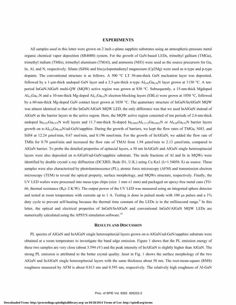
PL spectra of AlGaN and InAlGaN single heteroepitaxial layers grown on n-AlGaN/ud-GaN/sapphire substrate were
obtained at a room temperature to investigate the band edge emission. Figure 1 shows that the PL emission energy of
these two samples are very close (about 3.594 eV) and the peak intensity of InAlGaN is slightly higher than AlGaN. The
strong PL emission is attributed to the better crystal quality. Inset in Fig. 1 shows the surface morphology of the two
AlGaN and InAlGaN single heteroepitaxial layers with the same thickness about 50 nm. The root-mean-square (RMS)
roughness measured by AFM is about 0.813 nm and 0.595 nm, respectively. The relatively high roughness of Al-GaN
Proc. of SPIE Vol. 8262 826222-2
Downloaded From: http://proceedings.spiedigitallibrary.org/ on 04/28/2014 Terms of Use: http://spiedl.org/terms
single heteroepitaxial layer can mainly be attributed to the low deposition temperature of 830 °C necessary for the
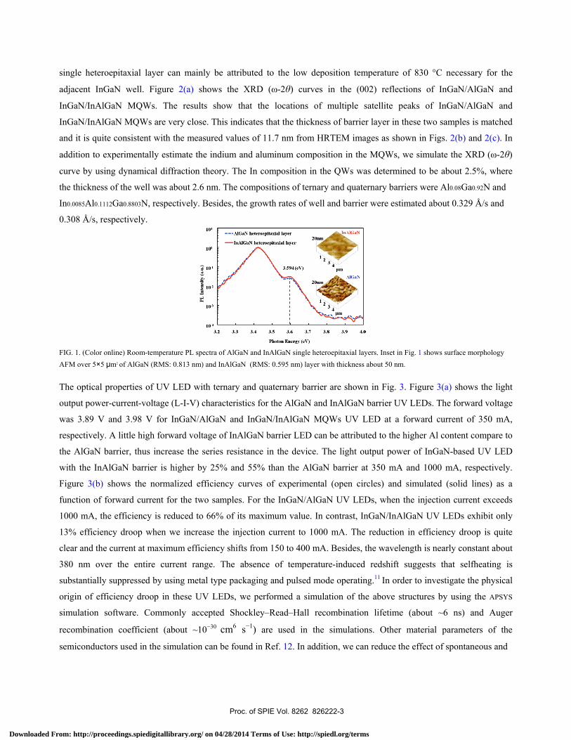
adjacent InGaN well. Figure 2(a) shows the XRD (ω-2θ) curves in the (002) reflections of InGaN/AlGaN and
InGaN/InAlGaN MQWs. The results show that the locations of multiple satellite peaks of InGaN/AlGaN and
InGaN/InAlGaN MQWs are very close. This indicates that the thickness of barrier layer in these two samples is matched
and it is quite consistent with the measured values of 11.7 nm from HRTEM images as shown in Figs. 2(b) and 2(c). In
addition to experimentally estimate the indium and aluminum composition in the MQWs, we simulate the XRD (ω-2θ)
curve by using dynamical diffraction theory. The In composition in the QWs was determined to be about 2.5%, where
the thickness of the well was about 2.6 nm. The compositions of ternary and quaternary barriers were Al0.08Ga0.92N and
In0.0085Al0.1112Ga0.8803N, respectively. Besides, the growth rates of well and barrier were estimated about 0.329 Å/s and
0.308 Å/s, respectively.
FIG. 1. (Color online) Room-temperature PL spectra of AlGaN and InAlGaN single heteroepitaxial layers. Inset in Fig. 1 shows surface morphology AFM over 5×5 μm2 of AlGaN (RMS: 0.813 nm) and InAlGaN (RMS: 0.595 nm) layer with thickness about 50 nm.
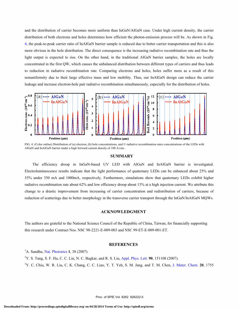
The optical properties of UV LED with ternary and quaternary barrier are shown in Fig. 3. Figure 3(a) shows the light
output power-current-voltage (L-I-V) characteristics for the AlGaN and InAlGaN barrier UV LEDs. The forward voltage
was 3.89 V and 3.98 V for InGaN/AlGaN and InGaN/InAlGaN MQWs UV LED at a forward current of 350 mA,
respectively. A little high forward voltage of InAlGaN barrier LED can be attributed to the higher Al content compare to
the AlGaN barrier, thus increase the series resistance in the device. The light output power of InGaN-based UV LED
with the InAlGaN barrier is higher by 25% and 55% than the AlGaN barrier at 350 mA and 1000 mA, respectively.
Figure 3(b) shows the normalized efficiency curves of experimental (open circles) and simulated (solid lines) as a
function of forward current for the two samples. For the InGaN/AlGaN UV LEDs, when the injection current exceeds
1000 mA, the efficiency is reduced to 66% of its maximum value. In contrast, InGaN/InAlGaN UV LEDs exhibit only
13% efficiency droop when we increase the injection current to 1000 mA. The reduction in efficiency droop is quite
clear and the current at maximum efficiency shifts from 150 to 400 mA. Besides, the wavelength is nearly constant about
380 nm over the entire current range. The absence of temperature-induced redshift suggests that selfheating is
substantially suppressed by using metal type packaging and pulsed mode operating.11 In order to investigate the physical
origin of efficiency droop in these UV LEDs, we performed a simulation of the above structures by using the APSYS
simulation software. Commonly accepted Shockley–Read–Hall recombination lifetime (about ~6 ns) and Auger
recombination coefficient (about ~10−30 cm6 s−1) are used in the simulations. Other material parameters of the
semiconductors used in the simulation can be found in Ref. 12. In addition, we can reduce the effect of spontaneous and
Proc. of SPIE Vol. 8262 826222-3
Downloaded From: http://proceedings.spiedigitallibrary.org/ on 04/28/2014 Terms of Use: http://spiedl.org/terms

piezoelectric polarizations because of lattice match condition in barrier between AlGaN and InAlGaN. The total
polarization fields in different combination of materials can be obtained through the calculation, and the results of
In0.025Ga0.975N, Al0.08Ga0.92N, and In0.0085Al0.1112Ga0.8803N are the −0.0305 (C m−2), −0.0391 (C m−2), and −0.0398 (C
m−2), respectively.13 Besides, a different bandoffset ratio from 6:4 to 7:3 is used in this simulation for introducing of
indium in AlGaN. We can know that under the same energy band of barrier, the band-offset ratio from 6:4 to 7:3 will
lead higher conduction-band and lower valence-band between well and barrier. This is useful for electron confinement
and hole distribution in low indium content InGaN-based UV LEDs. However, another difficult problem is the inclusion
of degenerate valence bands in minority carrier hole mobility. Hence, to investigate the efficiency droop in these two
samples, we assume that InGaNbased UV LED with InAlGaN barrier has relatively high carrier mobility. The values of
mobility for electron and hole are assumed in the simulation, μn-InGaN/AlGaN=354 cm2 /V s, μn-InGaN/InAlGaN=642 cm2 /V s, μp-
InGaN/AlGaN=2 cm2 /V s, and μp-InGaN/InAlGaN=5 cm2 /V s, respectively. Finally, the results of the EQE droop simulation of
both different structures are in good agreement with the experimental data as shown in Fig. 3(b). Finally, we have to
check the actual carrier distribution in our simulation.
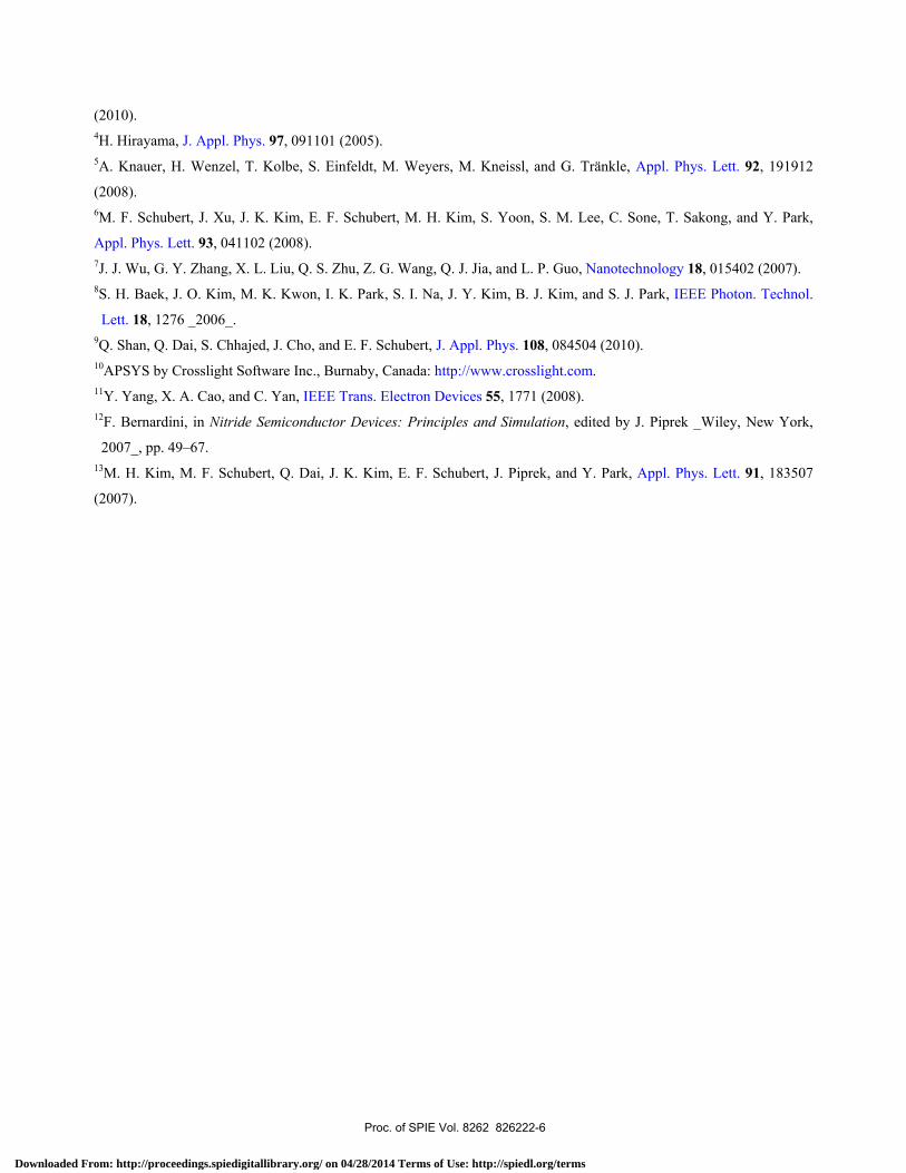
Figure 4 shows the calculated carrier distribution in these UV LEDs structure under a high forward current density
of 100 A/cm2 (1000 mA) by APSYS. When we apply the corresponding band-offset ratio and the carrier mobility in
InGaN/InAlGaN MQWs, the electron and hole concentration increases in the QW by about 26% and 35%, respectively,
FIG. 2. (Color online) (a) XRD ω -2 θ curves in the (002) reflections of InGaN/AlGaN and InGaN/InAlGaN MQW. Cross-sectional TEM images of (b) InGaN/AlGaN and (c) InGaN/InAlGaN MQW. The diffraction condition is g=0002.
FIG. 3. (Color online) (a) L-I-V curves of the LEDs with AlGaN (dash) and InAlGaN (solid) barrier. (b) Normalized efficiency curves of experimental (open circles) and simulated (solid lines). Inset in Fig. 3(a) shows the mesatype UV chip.
Proc. of SPIE Vol. 8262 826222-4
Downloaded From: http://proceedings.spiedigitallibrary.org/ on 04/28/2014 Terms of Use: http://spiedl.org/terms
and the distribution of carrier becomes more uniform than InGaN/AlGaN case. Under high current density, the carrier
distribution of both electrons and holes determines how efficient the photon-emission process will be. As shown in Fig.
4, the peak-to-peak carrier ratio of InAlGaN barrier sample is reduced due to better carrier transportation and this is also
more obvious in the hole distribution. The direct consequence is the increasing radiative recombination rate and thus the
light output is expected to rise. On the other hand, in the traditional AlGaN barrier samples, the holes are locally
concentrated in the first QW, which causes the unbalanced distribution between different types of carriers and thus leads
to reduction in radiative recombination rate. Comparing electrons and holes, holes suffer more as a result of this
nonuniformity due to their large effective mass and low mobility. Thus, our InAlGaN design can reduce the carrier
leakage and increase electron-hole pair radiative recombination simultaneously, especially for the distribution of holes.
FIG. 4. (Color online) Distribution of (a) electron, (b) hole concentrations, and © radiative recombination rates concentrations of the LEDs with AlGaN and InAlGaN barrier under a high forward current density of 100 A/cm2.
SUMMARY
The efficiency droop in InGaN-based UV LED with AlGaN and InAlGaN barrier is investigated.
Electroluminescence results indicate that the light performance of quaternary LEDs can be enhanced about 25% and
55% under 350 mA and 1000mA, respectively. Furthermore, simulations show that quaternary LEDs exhibit higher
radiative recombination rate about 62% and low efficiency droop about 13% at a high injection current. We attribute this
change to a drastic improvement from increasing of carrier concentration and redistribution of carriers, because of
reduction of scatterings due to better morphology in the transverse carrier transport through the InGaN/InAlGaN MQWs.
ACKNOWLEDGMENT The authors are grateful to the National Science Council of the Republic of China, Taiwan, for financially supporting
this research under Contract Nos. NSC 98-2221-E-009-003 and NSC 99-ET-E-009-001-ET.
REFERENCES 1A. Sandhu, Nat. Photonics 1, 38 (2007). 2Y. S. Tang, S. F. Hu, C. C. Lin, N. C. Bagkar, and R. S. Liu, Appl. Phys. Lett. 90, 151108 (2007). 3Y. C. Chiu, W. R. Liu, C. K. Chang, C. C. Liao, Y. T. Yeh, S. M. Jang, and T. M. Chen, J. Mater. Chem. 20, 1755
Proc. of SPIE Vol. 8262 826222-5
Downloaded From: http://proceedings.spiedigitallibrary.org/ on 04/28/2014 Terms of Use: http://spiedl.org/terms
(2010). 4H. Hirayama, J. Appl. Phys. 97, 091101 (2005). 5A. Knauer, H. Wenzel, T. Kolbe, S. Einfeldt, M. Weyers, M. Kneissl, and G. Tränkle, Appl. Phys. Lett. 92, 191912
(2008). 6M. F. Schubert, J. Xu, J. K. Kim, E. F. Schubert, M. H. Kim, S. Yoon, S. M. Lee, C. Sone, T. Sakong, and Y. Park,
Appl. Phys. Lett. 93, 041102 (2008). 7J. J. Wu, G. Y. Zhang, X. L. Liu, Q. S. Zhu, Z. G. Wang, Q. J. Jia, and L. P. Guo, Nanotechnology 18, 015402 (2007). 8S. H. Baek, J. O. Kim, M. K. Kwon, I. K. Park, S. I. Na, J. Y. Kim, B. J. Kim, and S. J. Park, IEEE Photon. Technol.
Lett. 18, 1276 _2006_. 9Q. Shan, Q. Dai, S. Chhajed, J. Cho, and E. F. Schubert, J. Appl. Phys. 108, 084504 (2010). 10APSYS by Crosslight Software Inc., Burnaby, Canada: http://www.crosslight.com. 11Y. Yang, X. A. Cao, and C. Yan, IEEE Trans. Electron Devices 55, 1771 (2008). 12F. Bernardini, in Nitride Semiconductor Devices: Principles and Simulation, edited by J. Piprek _Wiley, New York,
2007_, pp. 49–67. 13M. H. Kim, M. F. Schubert, Q. Dai, J. K. Kim, E. F. Schubert, J. Piprek, and Y. Park, Appl. Phys. Lett. 91, 183507
(2007).
Proc. of SPIE Vol. 8262 826222-6
Downloaded From: http://proceedings.spiedigitallibrary.org/ on 04/28/2014 Terms of Use: http://spiedl.org/terms