refinements to incremental transistor modelrmason/teaching/283-c.pdf · refinements to incremental...
TRANSCRIPT

Refinements to Incremental Transistor Model• This section presents modifications to the incremental models that
account for non-ideal transistor behavior
• Incremental output port resistance

• Incremental changes in the output port voltage cause incrementalchanges in the output port current
• rce and rds are commonly referred to as ro
• Typical values 20 kΩ - 100 kΩ

Input Port Resistances
• Accounts for the effects of any ohmic resistance that appears in serieswith the input port terminal
• Effects are particularly important in high frequency and high powerdevices
• Input port resistance can be taken into account by adding a resistancerx to the input port

Note: The incremental models do not take into account incremental capacitances which will be discussed in a later section.

Alternative BJT Representation
g ri
v
v
i
i
im beC
BE
BE
B
C
Bo= = =
δδ
δδ
δδ
β
• Since vBE and iB are related by the input port characteristics it is possibleto describe the output port in terms of vBE instead of iB


Two Port Representation of Incremental Circuits

Time Dependent Circuit Behavior
• The role of time dependence and frequency response is critical indetermining circuit behavior
• Many time-dependent properties can be modeled by the addition ofcapacitances to the PWL incremental model
• In very high speed circuits the addition of capacitances andinductances are necessary to model inter-connections between devices(parasitics)

Review of RC Circuits

• Response can be determined by using theappropriate differential equations or Laplacetransforms
• For a step function of the form
v t V u t u t
v t
v t V
v t V e
IN o
OUT
OUT o
OUT ot RC
( ) ( ) ( )
( )
( )
( ) ( )
"
/
= =
= == = ∞
= − −
step function
at t 0
at t
Time Domain"
0
1
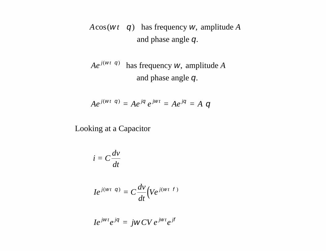
• In the time domain the V-I relationship for acapacitor is given by
i t Cd v t
dt( )
( )=

• In the frequency domain the impedencerepresentation transforms differential equationsinto simple algebraic equations
• Voltage and current variables are expressed ascomplex numbers (phasors) which have both amagnitude and phase
• From Euler’s formula
cos sin
cos sin
Re( ) cos
Im ( ) sin
tanRe( )
Im ( )
θ θ
θ θ
θ
θ
θ
θ
θ
θ
θ
θ
θ
+ =
= +
=
=
=
−
j e
Me M jM
Me M
Me M
Me
Me
j
j
j
j
j
j1
( )
A t A
Ae A
Ae Ae e Ae A
i Cdvdt
Ie Cdvdt
Ve
Ie e j CV e e
j t
j t j j t j
j t j t
j t j j t j
cos( )
.
.
( )
( )
( ) ( )
ω θ ωθ
ωθ
θ
ω
ω θ
ω θ θ ω θ
ω θ ω φ
ω θ ω φ
+
= = = ⟨
=
=
=
+
+
+ +
has frequency , amplitude
and phase angle
has frequency , amplitude
and phase angle
Looking at a Capacitor

[ ]
Ie j CV e
I j CV
I j CV
Vj C
I
Zj C
Z R Z j L
v v t Ve V t
j j
C
R L
INj t
θ φ
ω
ω
θ ω φ
ω
ω
ω
ω
ω
=
⟨ = ⟨
=
=
=
= =
= = =
1
1
Similarly:
If we apply an input sinusoid of the form
No phase angle
( ) Re cos
:

• The RC circuit can now be analyzed using thecomplex impedance representation
[ ]
v vZ
Z Zv
j C
j C R
v vj RC
vv RC
v RC
OUT INC
C RIN
OUT IN
OUT
IN
OUT
=+
=+
=+
=+
⟨ = −
1
1
11
1
1 2 1 2
1
ω
ω
ω
ω
ω
( )
tan
/

vv
j RCj RC j RC
j RC
R C
A j RC
OUT
IN
=−
+ −
=−
+
= −
1 1
1 1
1
1
1
2 2 2
( )
( )( )
( )
ωω ω
ωω
ω

• The analysis can also be performed on thefollowing circuit

• In the frequency domain the response to a singlefrequency sinusoid is given by
[ ]
v vZ
Z Zv
R
j C R
v vj RC
j RC
vv
RC
RC
OUT INR
R CIN
OUT IN
OUT
IN
=+
=+
=+
=+
1
1
1 2 1 2
ω
ωω
ω
ω( )/

⟨ = −
=+
−−
=+
+
= +
−v RC
v vj RC
j RCj RCj RC
R C j RCR C
A R C jA RC
OUT
OUT IN
π ω
ωω
ωω
ω ωω
ω ω
2
111 1
1
2 2 2
2 2 2
2 2 2
tan
( )( )

Bode Plot Representation
• For any linear circuit with a frequency dependent system function,both the magnitude and phase angle of the response are of greatinterest
• Often desirable to know these values over a wide frequency range
• Helpful to display information in graphical form called a Bode plot


• Common to express magnitude in decibels
dBvvOUT
IN
= 20 10log


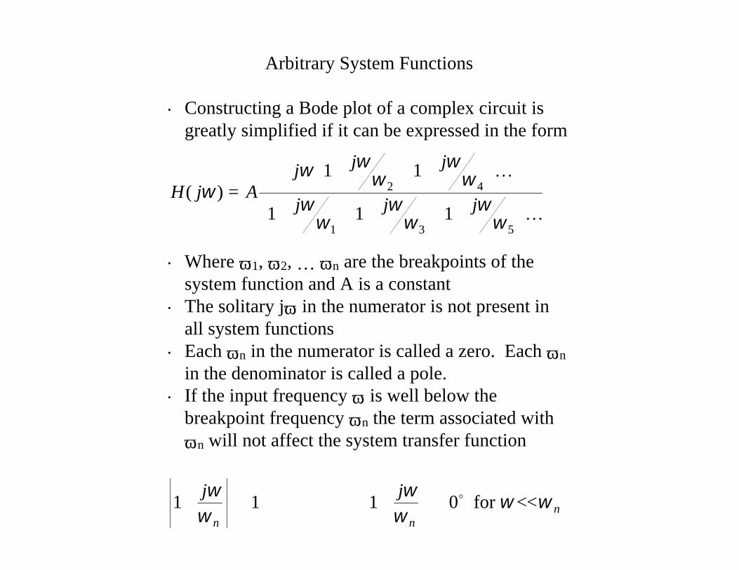
Arbitrary System Functions
• Constructing a Bode plot of a complex circuit isgreatly simplified if it can be expressed in the form
H j Aj j j
j j j( )ω
ω ωω
ωω
ωω
ωω
ωω
=+
+
+
+
+
1 1
1 1 1
2 4
1 3 5
K
K
• Where ω1, ω2, … ωn are the breakpoints of thesystem function and A is a constant
• The solitary jω in the numerator is not present inall system functions
• Each ωn in the numerator is called a zero. Each ωn
in the denominator is called a pole.• If the input frequency ω is well below the
breakpoint frequency ωn the term associated withωn will not affect the system transfer function
1 1+ ≅j
n
ωω
∠ +
≅ <<1 0
j
nn
ωω
ω ωo for

• If the driving frequency is well above ωn the termassociated with ωn will contribute a factor ω/ωn tothe magnitude and an angle factor of 90°
Hj
n n
ωω
ωω
≅
⟨ +
≅ = >>1 90
j j
n nn
ωω
ωω
ω ωo
• Given these guidelines the bode plot can be easilyconstructed. Beginning at a frequency far belowthe lowest breakpoint and increasing thefrequency. As the frequency passes through eachbreakpoint its term will contribute a factor ω/ωn tothe magnitude and 90° to the phase angle.
• If ωn is in the numerator the slope of the magnitudeBode plot shifts upward by a factor +20dB/decade. If ωn is in the denominator the slopewill shift downward -20 dB/decade.
• If ωn is in the numerator the angle will shift +90°.If ωn is in the denominator the angle will shift -90°.

• At the breakpoint the phase shift will be equal to± 45°
• If the solitary factor jω appears in the numeratorthe Bode plot will begin with a +20 dB/decadeslope and a phase angle of +90° at low frequencies
Problem:Construct a Bode plot for the following transfer function.
H jv t
v
j j
j jOUT
IN
( )( )ω
ω ω
ω ω= =+
+
+
501 10
110
1104 7
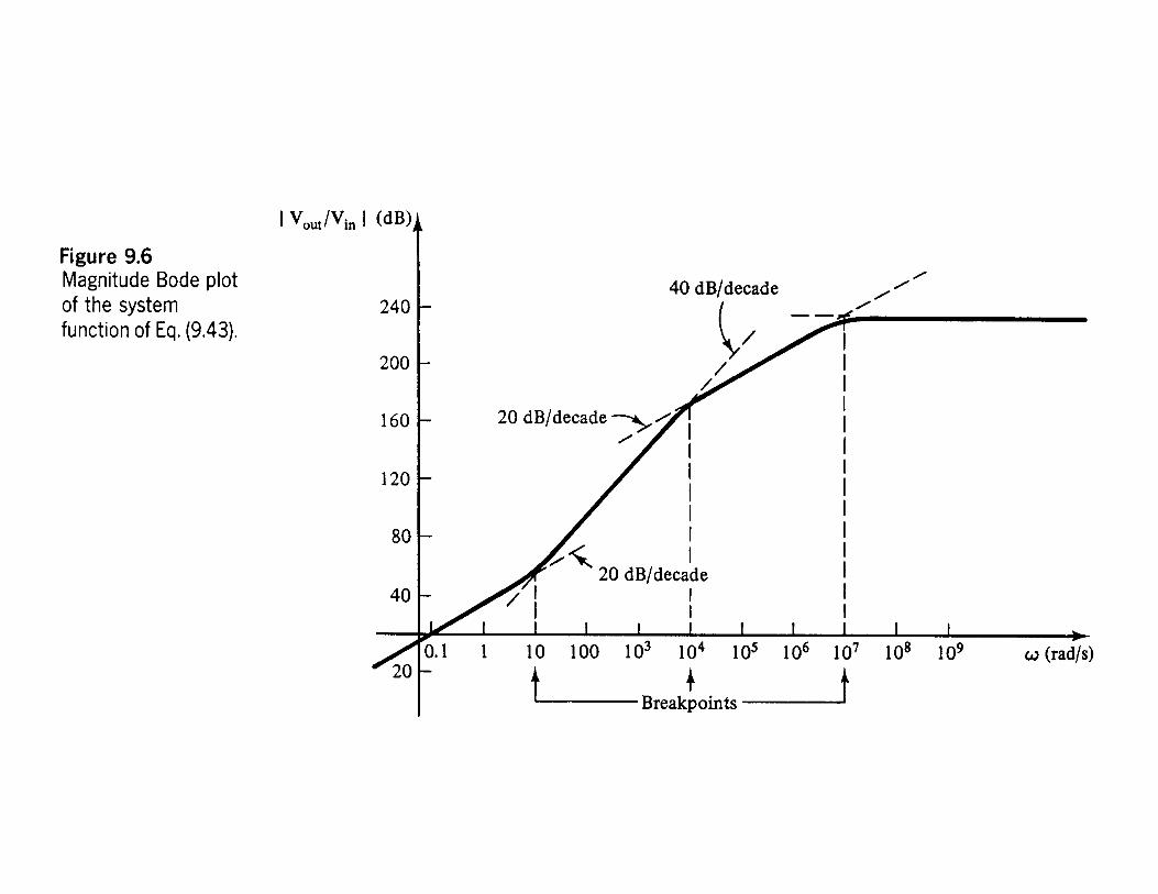

( )( )( )
( )( )at ω
ω ω
ω ω> ≅ = =10 50 10
10 10
50 10 10
102347
4 7
4 7vv
dBOUT
IN

Problem:Construct a Bode plot for the following function.
H jv j
v j jOUT
IN
( )( )ω ω
ω ω= =+
+
100
110
1104 4


Superposition of Poles
• Many applications require a constant response overa range of frequencies called the midband.
• The limits of the midband region may not coincidewith a single pole since multiple poles cancontribute to the output response
• Consider a system function as follows
H jj
j j j( )
( )
ω ωω ω ω
=+
+
+
1001 10 1
101
2 104 4x


HH
H
H H H
H
ω ωω
ω ω ω
ω
= =
+
+
+
=
≅
100
1 10 110
12 10
10002
0 84 10
2 1 2
4
2 1 2
4
2 1 2
4
/ / /
.
x
3 dB down from midband value
x rad / s

• It is possible to approximate ωL and ωH withmultiple poles using superposition of poles
• The system function is first put into the followingform
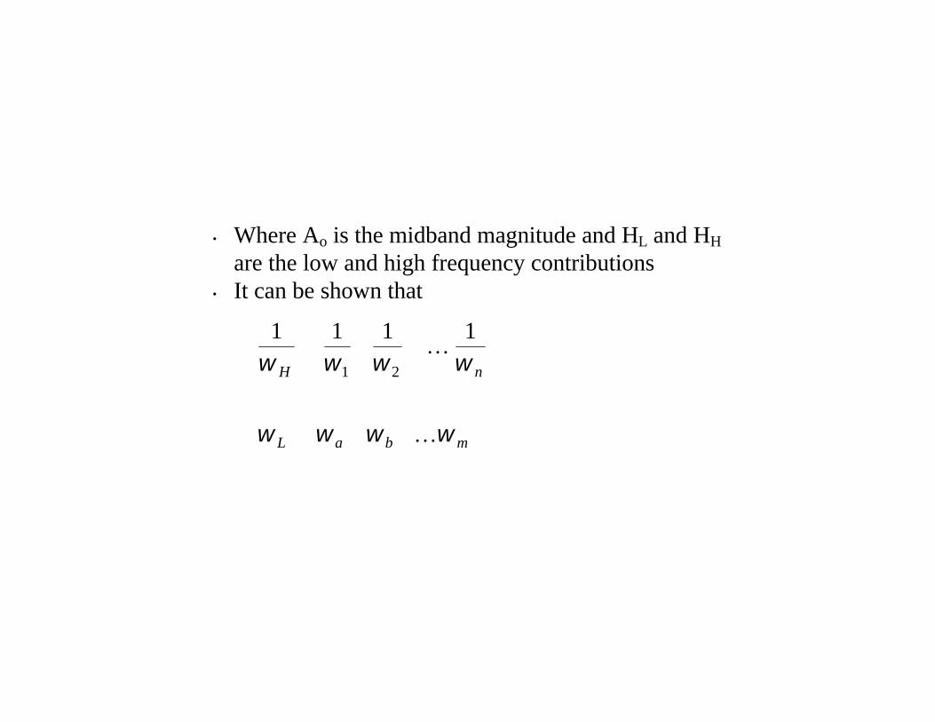
• Where Ao is the midband magnitude and HL and HH
are the low and high frequency contributions• It can be shown that
1 1 1 1
1 2ω ω ω ω
ω ω ω ω
H n
L a b m
≅ + +
≅ + +
K
K

Sources of Capacitance in Electronic Circuits• Capacitance plays a dominant role in shaping the time and frequency
response
• Inductances are usually important only well above breakpointfrequencies of major circuit capacitances
• Some exceptions include:– Power circuits using transformers
– RF circuits
– Oscillator circuits
– High speed digital circuits
– Filters
• Common sources of capacitance– Discrete capacitors
– Interconnect (stray) capacitance
– Internal capacitance of devices

Stray Lead Capacitance• Capacitance due to connections between devices
• Sometimes referred to as package capacitance
• Usually small < 10 pF
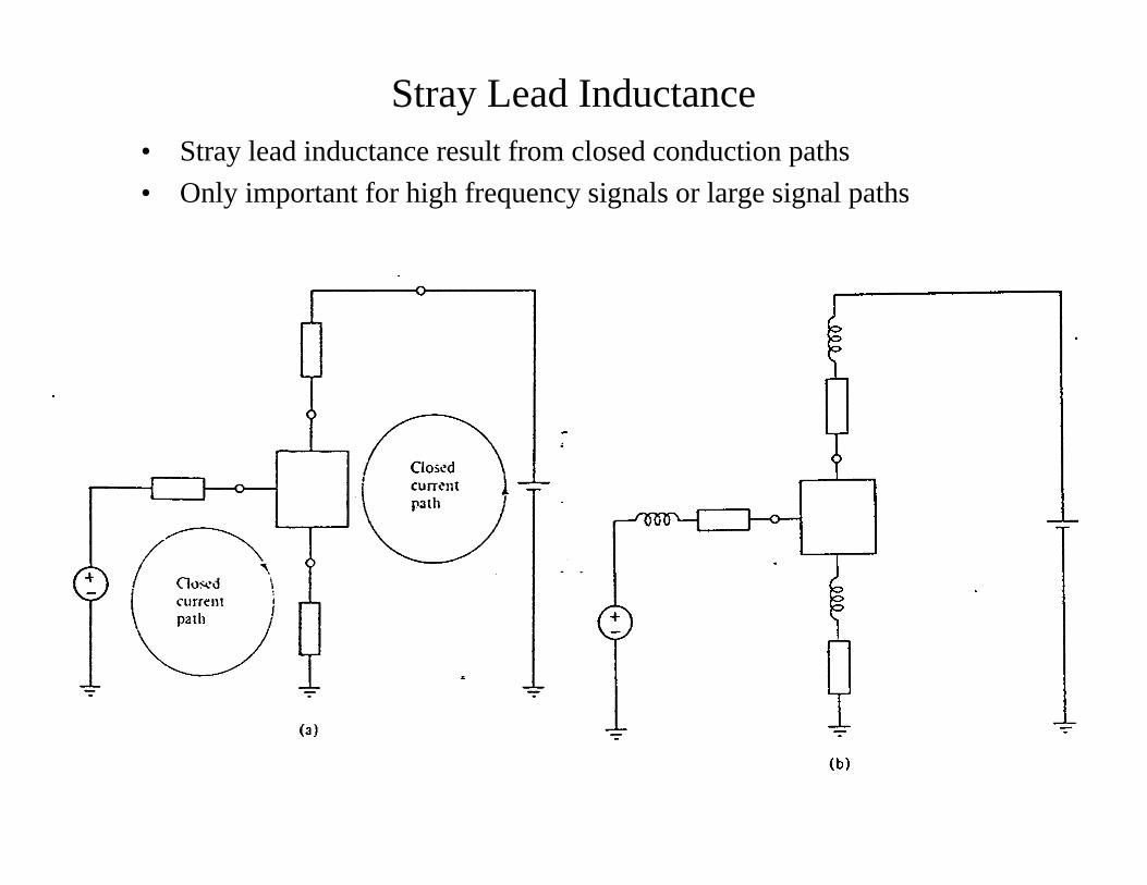
Stray Lead Inductance• Stray lead inductance result from closed conduction paths
• Only important for high frequency signals or large signal paths

Internal PN Junction Capacitance• PN junction forms the basis of Mos semiconductor devices
• The junction exhibits capacitance in both forward and reverse biasconditions
• This capacitance is usually much larger than stray capacitance andtherefore dominates frequency dependent behavior

Internal PN Junction Capacitance• As a result of junction capacitances we can develop a revised small
signal model of the BJT. This model is commonly referred to as theHybrid PI model.
• In most cases the base resistance rx can be ignored
• Important to note that the dependent source is dependent on the currentthrough rπ (i.e. iπ) not on the total base current ib
• It is possible to write gmvπ in terms of ib if the frequency dependenceof βo is taken into account
g v g r i i im m bπ π π ο π οβ β= = ≠( )

Internal PN Junction Capacitance

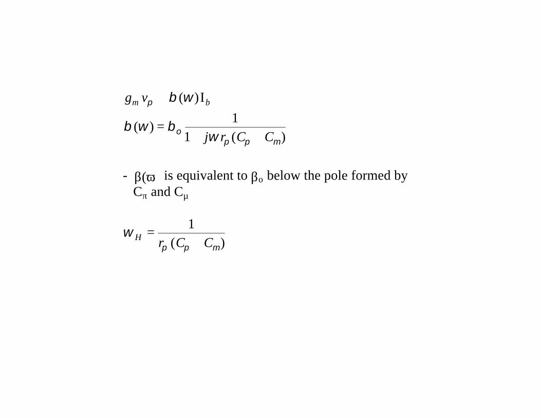
g v
j r C C
m bπ
οπ π µ
β ω
β ω βω
≅
=+ +
( )
( )( )
Ι1
1
- β(ω) is equivalent to βο below the pole formed by Cπ and Cµ
ωπ π µ
H r C C=
+1
( )


At Frequency ωT
β ω βω
ω ω
ω β
ω
οο
π π µ
π π µ π π µ
ο
π π µ π µ
π µ
( )( )
( ) ( )
( ) ( )
/
=+ +
=
+ +
≅ +
=+
=+
= −
11
1 2 22 1 2
j r C C
r C C r C C
r C Cg
C C
Cg
C
T
T T
Tm
m
T

MOSFET Model
• Similar models can be developed for other devices such asthe small signal MOSFET model below

Time and Frequency Response
• Presence of stray, internal and discrete circuit capacitance greatlyaffects the way electronic circuits respond to time-varying inputsignals
• Incremental step response of a transistor amplifier


v g R r v g R v
v v et r C
r R r
v g R v g R v et r C
OUT m c o m c
s
in s
in A
OUT m c m c s
in s
= − ≅ −
=−
=
= − = − −
( )
/ ( )
/
π π
π
π
π
for t > 0
• Small signal voltage decays to zero over time• Total output voltage returns to the DC bias value• In practice make Cs large such that
vv
g ROUT
s
m c
rin Cslim →∞
= −
• For the circuit in Fig. 9.24, Vcc = 5V, Cs = 1µF,RA= 1MΩ, RC = 3.3 kΩ, βF = βο = 200, Vf = 0.6V,η =1
• vin = square wave with Vp = 5mV


• rin Cs = 5.7 ms
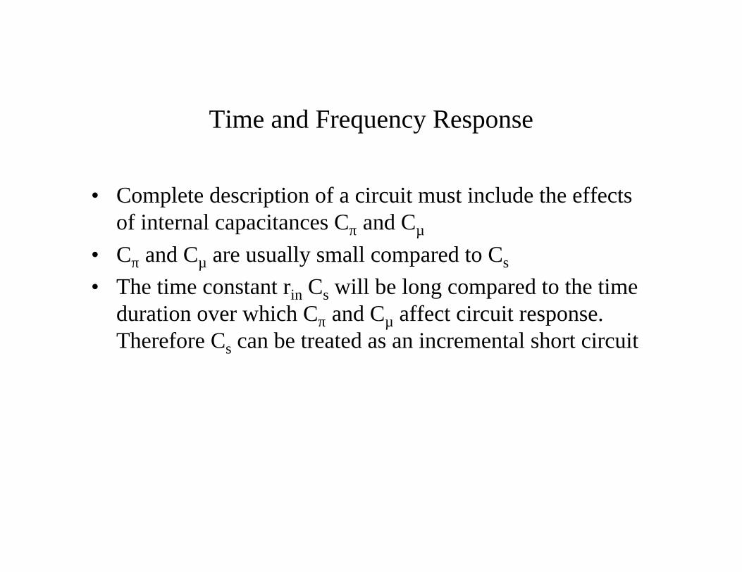
Time and Frequency Response
• Complete description of a circuit must include the effectsof internal capacitances Cπ and Cµ
• Cπ and Cµ are usually small compared to Cs
• The time constant rin Cs will be long compared to the timeduration over which Cπ and Cµ affect circuit response.Therefore Cs can be treated as an incremental short circuit


Using Miller’s Theorem
C Cv
v
C Cv
v
AOUT
BOUT
= −
= −
µπ
µπ
1
1
For Transverse Capacitance Cx
ZZ
VV
j Cj C
VV j C V
V
C C VV
C C VV
Ax
B
A
A
x
B
Ax
B
A
A xB
A
B xA
B
=−
=−
=−
∴ = −
= −
1
11
1
1
1
1
1
or
Similarly
ωω
ω

Miller’s Theorem
• Equivalence principle that can be applied to any port of a linear circuitthat is connected to another port by a transverse element

V I R V IVR
IV V
R
R RV
V V
RV
V
IVR
VR
V VV
V VR
R RV
V VRV
V
A A x B AA
A
AA B
x
A xA
A B
x
B
A
AA
A
A
x
A B
A
A B
x
B xB
A B
x
A
B
= + =
=−
=−
=−
= =−
=−
=−
=−
1
1
i.e.

Time and Frequency Response
• For the circuit configuration of figure 9.30 over the duration of theprincipal time constant the current through Cµ is negligible comparedto the current through gmvπ if gmrπ >> 1
[ ]
∴ = =
≅ −
≅ +
≅
i i g v g r i
v g R r
C C g R r
C C
m m
OUT m c o
A m c o
B
µ π π π π
µ
µ
( )
( )1

Time and Frequency Response
• Taking the Thevenin equivalent of vin, RA, rx and rπ results in thefollowing circuit

• The input loop has the same form as a simple RCcircuit for an input step function vs u(t)
v v e t r C C
v vr
r ru t
Ths A
Th sx
ππ
π
π
= − − +
=+
1 / ( )
( )
If rx << rπ then rs ≅ rx
v v e t r C C u t
v g v R r g R r e t r C C v u t
sx A
OUT m c o m c ox A
s
ππ
ππ
≅ − − +
= − = − − − +
1
1
/ ( ) ( )
( ) ( ) / ( ) ( )

• The principal time constant is rx(Cπ + CA)• The current source gmvπ will not be shorted out by
CB if:
( ) ( )R r C r C Cc o B x A<< +π
where (Rcro)CB is the time constant for CB