research archive - university of hertfordshire
TRANSCRIPT

Research Archive
Citation for published version:Qiwu Luo, Yigang He, and Yichuang Sun, “Real-Time Fault Detection and Diagnosis System for Analog and Mixed-signal Circuits of Acousto-Magnetic EAS Devices”, IEEE Design and Test, Vol. 33 (3), September 2015.
DOI: 10.1109/MDAT.2015.2480714
Document Version:This is the Accepted Manuscript version.The version in the University of Hertfordshire Research Archive may differ from the final published version. Users should always cite the published version of record.
Copyright and Reuse: © 2015 IEEE.Personal use of this material is permitted. Permission from IEEE must be obtained for all other uses, in any current or future media, including reprinting/republishing this material for advertising or promotional purposes, creating new collective works, for resale or redistribution to servers or lists, or reuse of any copyrighted component of this work in other works.
EnquiriesIf you believe this document infringes copyright, please contact the Research & Scholarly Communications Team at [email protected]
> DT-2015-05-0043.R1 <
1
Abstract—Real-time fault detection and diagnosis of analog and
mixed-signal circuits are challenging due to the large-scale integration and component tolerance. This paper presents a modular fault diagnostic system based on FPGA. Rather than dealing with the whole circuit directly, the proposed approach partitions a large-scale circuit into several small sub-circuits according to the circuit nature or signal flow and handles each sub-circuit by using two-dimensional information fusion, network analysis, and interval math theory. In the real applications of acousto-magnetic EAS products, two test examples are given to demonstrate the diagnosis performance for both pure analog and mixed-signal circuits. Results show the method’s high speed, effectiveness, and robustness.
Index Terms—Fault diagnosis, analog and mix-signal (AMS), circuit under test (CUT), field-programmable gate array (FPGA), electronic article surveillance (EAS)
I. INTRODUCTION ROM conventional fault dictionary, parameter identification and fault verification techniques to recent
neural network [1], fuzzy theory [2] and wavelet analysis [3] methods, the past five decades have witnessed an unprecedented development in the field of analog fault detection and diagnosis (AFDD) especially for the study of fundamental theory. And these sustainable theoretical achievements will be gradually applied to real world engineering to realize their contributions. In [4], a fast transient testing methodology for predicting the performance parameters of analog circuits was proposed, focusing mainly on analog ICs. Moreover, a remote AFDD method was developed based on LabVIEW in [5], its diagnosis results could be monitored on web browser. These studies show invariably that diagnosis speed and test cost should be emphasized simultaneously in the testing and diagnosis of analog and mixed-signal (AMS) circuits.
This work was supported by the National Natural Science Funds of China
for Distinguished Young Scholar under Grant No. 50925727, The National Defense Advanced Research Project Grant No.C1120110004 and 9140A27020211DZ5102, Hunan Provincial Science and Technology Foundation of China under Grant No.2010J4 and 2011JK2023, the Key Grant Project of Chinese Ministry of Education under Grant No.313018.
Q. Luo is with the College of Electrical and Information Engineering, Hunan University, Changsha 410082, China (e-mail: [email protected]).
Y. He is with the School of Electrical and Automation Engineering, Hefei University of Technology, Anhui, China (e-mail: [email protected]).
Y. Sun is with the School of Engineering and Technology, University of Hertfordshire, Hatfield ALl0 9AB, U.K. (e-mail: [email protected]).
Electronic article surveillance (EAS) detection devices are used to evaluate human exposure to designated electromagnetic fields [6]. Although the RFID technology has been revealing its ambition in expanding its range of application, the acousto-magnetic (AM) technology due to owning more reliable performance is dominating today's EAS industry. The normal operating of EAS systems are directly linked to the economic benefits both in the apparel industry and in retail. Until 2012, although retailers had introduced EAS technologies, around 25% of the most-stolen products still had no specific protections [7], needless to say that when the equipped EAS systems are off-normal. For a general AM-EAS detection system, the electronic control board (ECB), being the most vital constituent part, is a typical large-scale AMS circuit. And these kinds of soldered printed circuit board (PCB) are continuously operating in EAS equipments to support the non-stop profit protection by reducing shoplifting, theft and vendor fraud. However at present, the common handling method on the faulty ECBs is to replace them with brand-new ones by their suppliers, and then diagnose the possible faults offline. Such solutions have caused economic and time losses to both EAS device suppliers and retailers.
On the other hand, FPGA is by far parallel and highly reconfigurable, permitting rapid prototyping of control mechanisms and new algorithms for pre-research and realistic applications. These advantages show an opportunity to set up practical AFDD systems for the AM-EAS devices. In the recent past, FPGA has been widely applied for real-time power converter failure diagnosis, vibration analyses for industrial applications, and ionizing radiation detection for environmental awareness among many others. However, to our knowledge, FPGA-based real-time analog circuit diagnosis for AM-EAS products has not been available.
This paper mainly extends our previous diagnosis method by fusing information of gain-frequency and node voltages [8, 9]. Considering that the circuit accessible node voltages, responses of amplitude-frequency (A-F) and phase-frequency (P-F) contain abundant fault information, a FPGA-centered fault diagnosis prototype based on the above mentioned three circuit features is developed. The interval-math-based diagnosis algorithm is then tested on the realized prototype.
Real-Time Fault Detection and Diagnosis System for Analog and Mixed-signal Circuits of
Acousto-Magnetic EAS Devices Qiwu Luo, Yigang He, Yichuang Sun, Senior Member, IEEE
F
> DT-2015-05-0043.R1 <
2
The structure of the paper is as follows. Section II focuses on fault diagnosis theory, including how to extract the A-F and P-F parameters in real time. Following the theory, Section III presents the hardware topology of the diagnosis prototype and some key implementation details are described as well. Two experimental cases and their test results are shown in Section IV and Section V to prove the effectiveness of the proposed method. And finally, Section VI gives our conclusions and ideas for future work.
II. FEATURE EXTRACTION AND DIAGNOSIS THEORY This section firstly introduces our circuit fault feature
extraction method, and the orthogonal algorithm which is conducive to FPGA realization is also presented in detail. Then the diagnosis methods and judging rules using the techniques of interval math and information fusion are presented.
A. Approaches of Amplitude and Phase Detection Many recent publications show that the node-voltage-based
diagnostic methods are becoming increasingly mature [9]. Hence we only describe the real-time data acquisition approach of the A-F and P-F characteristics to avoid cumbersome.
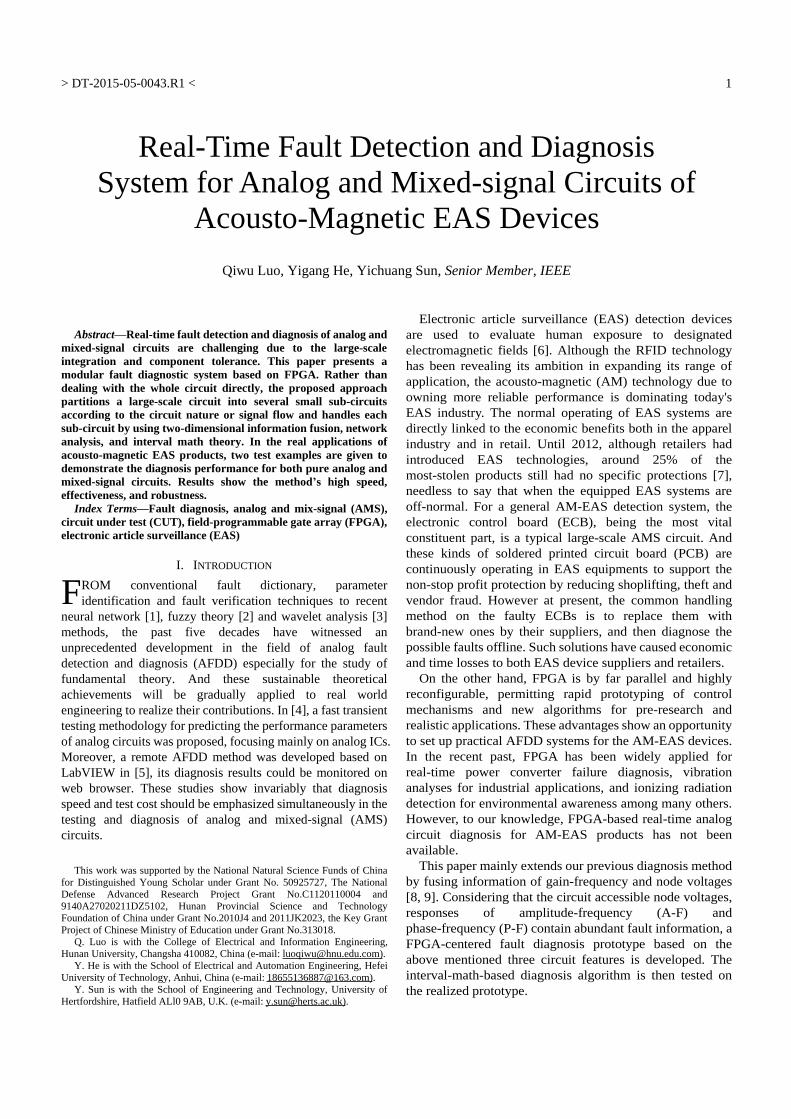
Digital amplitude and phase discriminations are extensively applied in intermediate frequency domain, which means it is practicable to adopt digital analysis approaches to fault diagnosis of large-scale AMS circuits. The data acquisition scheme is shown in Fig. 1. In order to diagnose the potential failure, we partition the whole small-signal-processing circuit into several small sub-networks according to the signal flow.
whole network
sub-network1
sub-networkN……
detection & diagnosis system
DAC ADC1 ADC2
y1
y2
y
Fig. 1. Testing diagram for analog network.
Supposing that the excitation signal on the DAC terminal is defined as y = sin(wt), the input and output signals of a certain sub-network are respectively expressed as y1(t) = A1 sin(wt+ϕ) and y2(t) = A2 sin(wt+θ), which are fed back into the fault detecting system via ADC1 and ADC2 ports. Then the amplitude, phase and network gain can be calculated according to (1)-(7) using orthogonal algorithm.
1( ) cos( )11 10
1 1 2 1sin( ) sin sin1 2 10 2 2 2
H nT wnTk y
n H HH wnT H
A A An H
φ φ φ
−= ×∑
=−
= + + =∑=
(1)
1
1 1
1( ) sin( )12 0
1 1 1 2cos cos( ) cos
0 2 2 2
H nT wnTk y
n H HH wnT H
A A An H
φ φ φ
−= ×∑
=−
= − + =∑=
1
(2)
2 2
1( ) cos( )21 20
1 1 1sin( ) sin sin20 2 2 2
H nT wnTk y
n H HH wnT H
A A An H
θ θ θ
−= ×∑
=−
= + + =∑=
(3)
2
1( ) sin( )22 20
1 1 1 2cos cos( ) cos2 20 2 2 2
H nT wnTk y
n H HH wnT H
A A An H
θ θ θ
−= ×∑
=−
= − + =∑=
(4)
11 12
2 2 2 21 11 12
(1) (2) tan( )
(1) (2) (2 )
ac k k
A H k k
φ⇒ =
+ ⇒ = +
(5)
21 22
2 2 2 22 21 22
(3) (4) tan( )
(3) (4) (2 )
ac k k
A H k k
θ⇒ =
+ ⇒ = +
(6)
2 1gainNetwork A A= (7)
where k11 and k12 are the intermediate variables derived from y1(t) and y, while k21 and k22 are the intermediate variables derived from y2(t) and y, T is the period of excitation signal, H is its quantization number per single period after discretization.
Because AM-EAS detection devices avoid item shrinkage of retail sales basically via magnetically-coupled resonant circuits tuned at a defined central frequency with an assigned bandwidth, usually 57.8 kHz ~ 58.2 kHz, the receiver sub-networks are handling these 2- amplitude shift keying (2-ASK) signals to identify whether the item under monitoring is already-paid or stolen. Unlike the narrow bandwidth of AM-EAS tags, the overall bandwidth of the receiver circuits is set to 5 kHz to maintain necessary margin for potential frequency deviation. Correspondingly during the implementation, the frequency of the excitation signal y is scanned with a pre-configured step within the 5 kHz bandwidth, the A-F and P-F parameters can then be obtained from (5) ~ (7), which constitute the fault feature vectors together with the accessible node voltages.
B. Theory of Fault Diagnosis
a) Parameter selection of the feature interval As hard fault is a special case of soft fault, thus, we treat all
fault modes as soft fault type. The three parameters of node voltages, A-F and P-F characteristics form the circuit feature vector (FV) in (8).
1 1 1 2 1 3, , , , , , ,
N N Nn n a a p pFV f f f f f f = L L L (8)
where, fn, fa, fp represent the features of node voltage, A-F and P-F respectively, N1, N2, N3 are their relevant totalities. For simplifying the derivation, here we define N as the sum of them, hence we can rewrite (8) as
[ ]1 2, , , NFV f f f= L (9)
where fj (j=1,… ,N) is the jth circuit parameter of the feature vector. Then we suppose there are M circuit modes
> DT-2015-05-0043.R1 <
3
including faulty and normal ones, then the feature interval vectors can be defined as
[ ]1 1 2 2( , ), ( , ), , ( , ) , 1, ,i i i i i iN iNFI L R L R L R i M= =L L (10) where Li j, Ri j are respectively the lower and upper bound
of the jth circuit parameter of the ith circuit mode. The feature interval reflects the circuit mode to some degree as it is composed by the circuit parameter intervals, which can be simulated by PSpice with Monte-Carlo method.
b) Circuit similarity of test sample to the feature interval vectors
The feature interval represents the circuit mode so that the circuit mode could be identified by calculating the correlation degree of the test sample to the feature interval vectors. According to the fuzzy pattern recognition theory, membership degree reflects the correlation of the test sample to the mode feature vector. Referring to this relationship, the circuit similarity is selected to depict the correlation of the sample and the feature interval vectors, which is defined as follows.
Suppose that the test sample (TS) is expressed by (11). [ ]1 2, , , NTS ts ts ts= L (11)
then, εi j, namely “interval similarity” of the test sample TS to the feature interval (Li j, Ri j) can be defined as
ηεη
=
∈= − ∉
∑1
1,( , )
1 ,( , )ijij M
iji
i j I
i j I (12)
In (12), I = {(i, j) | Li j ≤ tsj ≤ Ri j, i=1,…,M, j=1,…,N }, and ηi j is the so-called “interval relative distance” of TS to the feature interval (Li j, Ri j), which can be expressed as (13), where min represents the minimum value in its { }.
{ }η
− −= =
−L
min ,, 1, ,
j ij j ij
ij
ij ij
TS L TS Rj N
L R (13)
The nearer the tsj is to either boundary of the feature interval (Li j, Ri j), the wider the feature interval, the shorter the interval relative distance ηi j and the larger the interval similarity εi j (but less than 1). Only when Li j ≤ tsj ≤ Ri j, then εi j reaches 1. Furthermore,
ε ε=
= =∑ L1
1, 1, ,
N
i ijj
i MN
(14)
εi represents the average circuit similarity of the TS to the ith feature interval vector under information fusion of N circuit parameters.
c) Diagnosis rules using information fusion The responses of the tolerance circuit under different modes
are sometimes so similar and difficult to distinguish, which means that a certain test sample would belong to several circuit modes. So only from a single dimensional array of circuit parameters, the diagnosis result may be unreliable. To solve this problem, a multi-frequency-based information fusion approach is applied in this paper.
Without loss of generality, the total number of the frequency sampling points P can be expressed in (15), where W and F are
respectively the frequency bandwidth and scanning step. For a typical AM-EAS system, signals within the frequency range of 55.5 kHz ~ 60.5 kHz will be handled by the band-pass filter of the receiving circuits. Specifically, if the frequency step is set as 50 Hz, the total number P equals 100.
= =( )/ ( )W
P W Hz F HzF
(15)
Then the circuit similarity matrix of the TS to circuit modes is defined as
ε ε ε Γ = = = L L L1 2, , , , 1, , , 1, ,
i i ipi M k P (16)
where εi k is circuit similarity matrix under multi-frequency inputs, M and P are respectively the totalities of circuit modes and the selected frequency points. Furthermore, we assume that the reliability of different input with different frequency is ω ω ω= L
1( , )T
P (17)
Then the final similarity matrix of the TS to circuit modes can be rewritten as ε ω ε ε ε = Γ × = L
1 2, , ,
T
M (18)
where,
ε ε ω=
= =∑ L1
, 1, ,P
i ik kk
i M (19)
Based on the circuit similarity εi defined in (14), εi in (19) represents the final similarity of the test sample TS to the ith circuit mode under information fusion of N circuit parameters and P frequency responses.
According to literature [9], ωk (k=1, …, P) in (17) can be computed by the method as below,
{ }ω α β α β α ε β α ε=
= =
= = =∑ ∑1
1 1
, max ,MP M
k k k k k k ik k k iki
k i
(20)
The larger the final similarity, the higher the probability that the corresponding component is the faulty one. Then we define the maximum final similarity, the second final maximum similarity and the average value of final similarity matrix as εmax1, εmax2 and εavg respectively. Finally, the rules for fault location is defined in accordance with the following regulations.
The fault component is the one possessing the maximum final similarity if
(a) εmax1 is more than threshold δ and (b) the difference between εmax1 and εmax2 is more than
threshold σ. if (a) and (b) are not met, then if (c) the ratio between εmax1 and εavg is more than λ. The fuzziness of two or more components results mainly
from the fact that they take up the same maximum final similarities, which makes the decision rules not work. As we have adopted the two-dimensional information fusion technique (based on N circuit parameters responding to P frequency points), the fuzziness is decreased to a large extent.
III. PROTOTYPE STRUCTURE DESIGN According to the foregoing analysis, we aim to set up an
AFDD prototype with high adaptability in this section. The

> DT-2015-05-0043.R1 <
4
proposed hardware scheme is shown in Fig. 2, the chip model of the processor is XC3SD3400A (belongs to Spartan-3A DSP series, Xilinx Inc.). The signal generation part consists of the digital to analog converter (DAC902, 165Msps/12-Bit) and the direct digital synthesizer (DDS) IP core. Then, the frequency sweep signal can be generated from SAM1 port, playing a role of the excitation signal source for CUTs. When it comes to the data acquisition part, there are two different signal objects. For small AC signals, the selected MAX12529 is a dual channel signal acquisition chip having high-performance up to 96Msps/12-Bit. Hence the input/output signals of a certain sub-CUT can be captured by this system through SMA2 and SAM3 simultaneously. For DC signals, in order to simplify design and enhance the flexibility, an extendible sub-board is developed and node voltages can be imported via the PIN array interface conveniently. As for the DSP cores array, it is the computing center of diagnosis algorithms and mainly composed of advanced DSP48E slices, look-up tables (LUTs), true dual-port RAM blocks, first input first output (FIFOs) and share memories. Engineers can reconfigure it flexibly for their specific purpose. At the same time, the system is integrated with sufficient double data rate 2 synchronous dynamic random access memory (DDR2-SDRAM) and flash memory, which support data cache for diagnostic algorithms and backup of intermediate variables. What is more, the raw captured data and analysis results can be transmitted to host server via Ethernet for subsequent processing if necessary. Another significant technology worthy of being emphasized is that all the intellectual property (IP) cores are managed by MicroBlaze (a 32-bit embedded software processor) via processor local bus (PLB). As a prototype, it provides some redundant functions, while in the final engineering applications, the whole scheme should be tailored according to the specific nature of the CUT. And the realized diagnosis platform is given in Fig. 3.
SMA1SMA2SMA3
DDR2
PIN1-16
FPGA
UART
Ethernet
Fig. 3. The FPGA-based diagnosis platform.
IV. ILLUSTRATIVE CIRCUITS AND FAULTS A typical ECB of AM-EAS detection system consists of
power supply, transmitter, receiver and DSP controller, where only controller part belongs to digital circuit, the other three are AMS circuits. At present, the popular EAS device has self diagnostic function for its transmitter relying on over-current and over-temperature techniques. Consequently, the following two CUTs mainly focus on power supply and receiver parts, including a switching mode power supply (SMPS) and a multi-stage band-pass filter (BPF). The resistors and capacitors have tolerance values of 1% and 5%, respectively. These two examples illustrate the method for the extraction of feature parameters and the fault diagnosis technique of AMS circuits developed in the previous sections, and we assume that there is an independent relationship between the considered faults for avoiding virtually unlimited testing clusters [10].
ADC chipMAX12529
high speeddata
acquisitiondrive
MPMC
DDR2 SDRAM(1GB)
MACcontroller
MicroBlaze
RJ-45
PLB bus
CRS
TX_CLKTXD(4:0)RX_CLKRXD(4:0)
MDCserialcontroller MDIO
SDDrive
SD card
MAX3232
nodevoltage
acquistiondrive
CLKPCLKN
A-inPA-inN
B-inPB-inN
c-bus
d-bus A
d-bus B
power system
PHY chipLAN83C185
RS232
SMA2
SMA3
data acquisition sub-board
PINarray
c-bus
d-bus
channel1
……
channelN
DAC chipDAC902filter DDS
IP core
c-bus
d-busSMA1
diff-clk
flashDrive
FLASH array
UARTcontroller
pre-processing
pre-processing
DSPcoresarray
Fig. 2. Topology structure of the proposed analog fault detection and diagnosis system. It is organized according to the direction of signal flow (which is from left to right), and all the modules in the dotted grey box are implemented in FPGA chip. The interfaces of SMA1, SMA2 and SMA3 correspond to the DAC, ADC1 and ADC2 ports defined in Fig.1, respectively.

> DT-2015-05-0043.R1 <
5
A. Example 1: Switching mode power supply (SMPS) The SMPS circuit, being the significant precondition of
normal working to the whole ECB, is mainly composed of pulse-width modulation (PWM) controller (U1), isolation transformer (T1), three nonlinear half-wave rectifier units (CR1 and C4, CR4 and C9, CR5 and C6) and feedback sub-circuit (centred on U3, U4). The nominal values and chip models for the components are shown in Fig. 4. We will study the availability of our method for nonlinear circuits suffered with hard and soft faults. The considered fault classes include the hard faults caused by open- or short-circuiting C4 ~ C9, C14, CR1, CR4 and CR5 and the soft faults caused by changing the value ratio of R9 and R13 from their correct 3.83 to erroneous 1 or 5.
Among the signals on all the accessible test points from TP1 to TP12, only that on TP5 is an AC signal which is the PWM output wave generated by U1, the remaining are DC level signals. Hence, we will extract the actual signals using input terminals (refer to Fig. 2) of SMA2 and PIN array respectively for data on TP5 and those on the others. As this circuit is not a typical two-port network and mainly related to DC-levels, multi-frequency fusing method has not yet been activated. To sum up, the discussed totalities of circuit modes M and parameters N equal 14 and 12, respectively, and that of frequency responses P is set to the reserved 1. Special emphasis to the test setup on this CUT is that, there are two ground planes isolated by T1,any short-circuiting is not allowed throughout the testing process, so we have equipped corresponding electrical isolation circuits to the pre-processing hardware parts in the proposed AFDD platform.
Then, the feature interval vectors FI and decision thresholds δ, σ, λ are trained on PSpice platform through Monte-Carlo simulations for several certain times. In our
design, we compute the “interval similarity” ε in (12) through around 1000 times of training. The simulations can also be verified on our realized AFDD system by changing the considered component values on the CUT. Limited by the engineering feasibility, the actual check of the trained values can only be performed in the form of sampling. The final values of FI, δ, σ and λ can not be programmed on FLASH ROM until the requirement that true-positive rate (TPR) is no less than 95% is met.
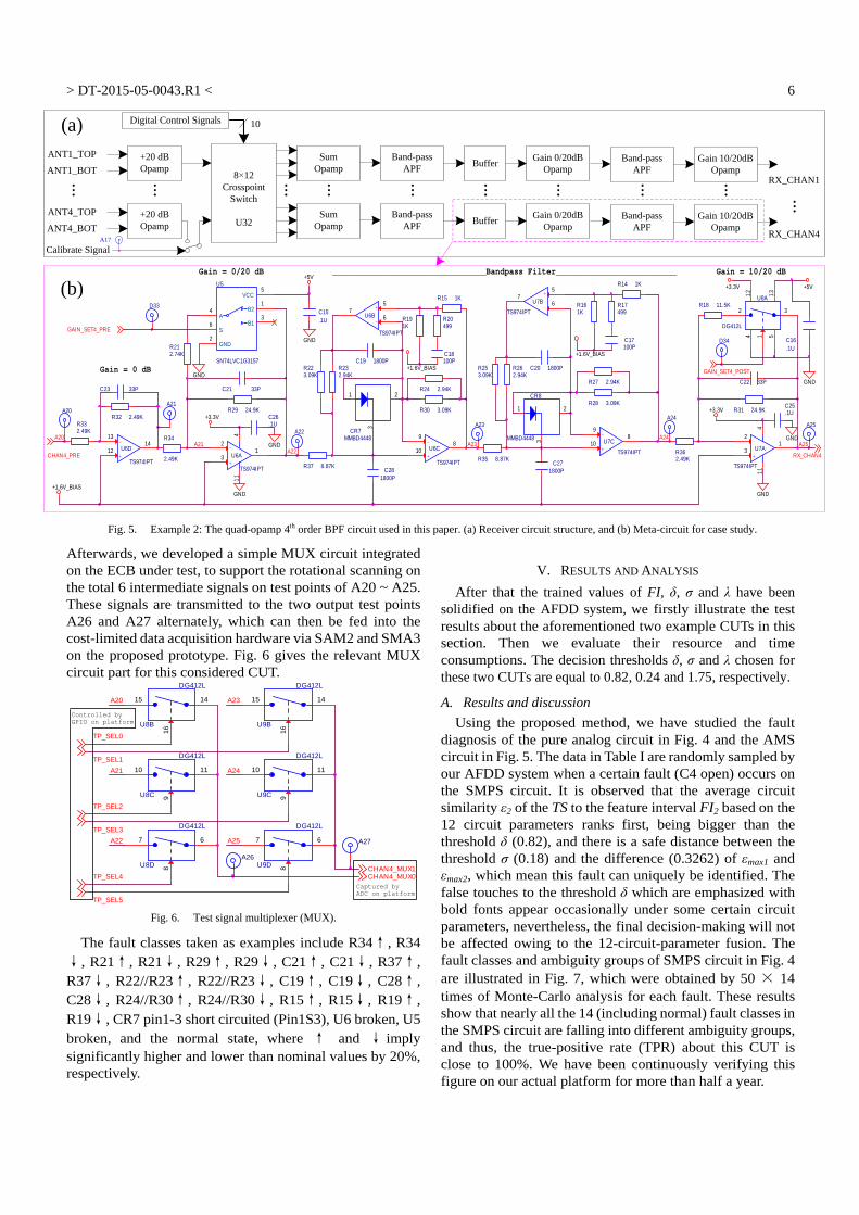
B. Example 2: Quad-opamp 4th order band-pass filter (BPF) A flagship AM-EAS system commonly supports 4
transmit-receive channels such as Ultra Exit Series reported in [7]. We firstly partition the receiver into several functional sub-modules trying to find the meta-circuit for case study in Fig. 5a. The signal outputs of the first stage amplifiers are fed into a cross-point switch which allows the signals to be routed to four later amplifier channels in a variety of combinations. Such logic circuitry part is handled through digital method which is beyond the discussion scope in this paper. So we select a representative AMS meta-circuit as the second test example and is shown in Fig. 5b, this is a quad-operational-amplifier (opamp) 4th order BPF circuit with programmable pre- and post- amplifiers, and its center frequency and bandwidth are respectively 58 kHz and 5kHz.
In order to simplify the circuit parameter vectors, this test should not be started until the power supply test is passed. In other words, this test is undergoing with normal power supplies on the nets of +5V, +3.3V and +1.6V_BIAS. The controlling level signals on test points of D33 and D34 are fed into PIN array on the FPGA-based platform for obtaining the gain of the relevant amplifiers. As for the small AC signals, sinusoidal excitation signals sweeping with a 250 Hz step varying from 55.5 kHz to 60.5 kHz are input via the test point A17 (shown in Fig. 5a) to this CUT.
TP4
HV_COM TP5PWM
TP2+12V_FB
TP11V_REF
TP12V_DIV
TP10V_FB
TP7+12V_AUX
TP9+12V_U5
R6260
R3130
CR3
CMPD914
CR6CMPZ5230
FL1
31/100M
R4
4.7
C3
.0022UF
TP1+325V_IN
R70.5
U3
OPT-C 817B
1
2
4
3
C810UF10V
+ C1110UF
R81.2K
C13 .01UF
C10.047UF
U1
ICE3A2065
Drain44
CS3
VCC7
GND8
FB2
Sof tS1
NC6
Drain55
+C41000UF35V
TP6GND
C14700P
+ C2100UF R1
200K
FL2
31/100M
R223.2K
+ C6
1000UF10V
T1
XFMR-10P2
1
5
4 7
6
8
10
9
CR4CMR1U-02
CR5 MBRS140T3
R51K
U4TL431A2
3
1
TP3+12V_OUT
+ C9330UF
C141000PF
U2LM2940
VI1
GND22
VO3
GND44
L2 100UH CR2MURS160T3
C12 1000PF
L1 100UH
R12 560
R10 22.1
CR1
CMR1U-02
TP8+5V_OUT
HV_COM
R134.99K
R919.1K
HV_REF
+325V
R11 57.6K
C710UF10V
+C5100UF35V
+12V_FB
HV_COM
HV_COM
HV_COM
HV_COM
HV_COM
HV_COM
HV_COM Fig. 4. Example 1: PWM-based SMPS circuit used in this paper.
> DT-2015-05-0043.R1 <
6
Afterwards, we developed a simple MUX circuit integrated on the ECB under test, to support the rotational scanning on the total 6 intermediate signals on test points of A20 ~ A25. These signals are transmitted to the two output test points A26 and A27 alternately, which can then be fed into the cost-limited data acquisition hardware via SAM2 and SMA3 on the proposed prototype. Fig. 6 gives the relevant MUX circuit part for this considered CUT.
U8B
DG412L
16
15 14
U8C
DG412L
9
10 11
U8D
DG412L
8
7 6
U9B
DG412L
16
15 14
U9C
DG412L
9
10 11
U9D
DG412L
8
7 6
A20 A23
A22
A21
A25
A24TP_SEL1
TP_SEL0
TP_SEL3
TP_SEL2
TP_SEL5
TP_SEL4
A27
CHAN4_MUX0CHAN4_MUX1
A26
Captured byADC on platform
Controlled by GPIO on platform
Fig. 6. Test signal multiplexer (MUX).
The fault classes taken as examples include R34↑, R34↓, R21↑, R21↓, R29↑, R29↓, C21↑, C21↓, R37↑, R37↓, R22//R23↑, R22//R23↓, C19↑, C19↓, C28↑, C28↓, R24//R30↑, R24//R30↓, R15↑, R15↓, R19↑, R19↓, CR7 pin1-3 short circuited (Pin1S3), U6 broken, U5 broken, and the normal state, where ↑ and ↓ imply significantly higher and lower than nominal values by 20%, respectively.
V. RESULTS AND ANALYSIS After that the trained values of FI, δ, σ and λ have been
solidified on the AFDD system, we firstly illustrate the test results about the aforementioned two example CUTs in this section. Then we evaluate their resource and time consumptions. The decision thresholds δ, σ and λ chosen for these two CUTs are equal to 0.82, 0.24 and 1.75, respectively.
A. Results and discussion Using the proposed method, we have studied the fault
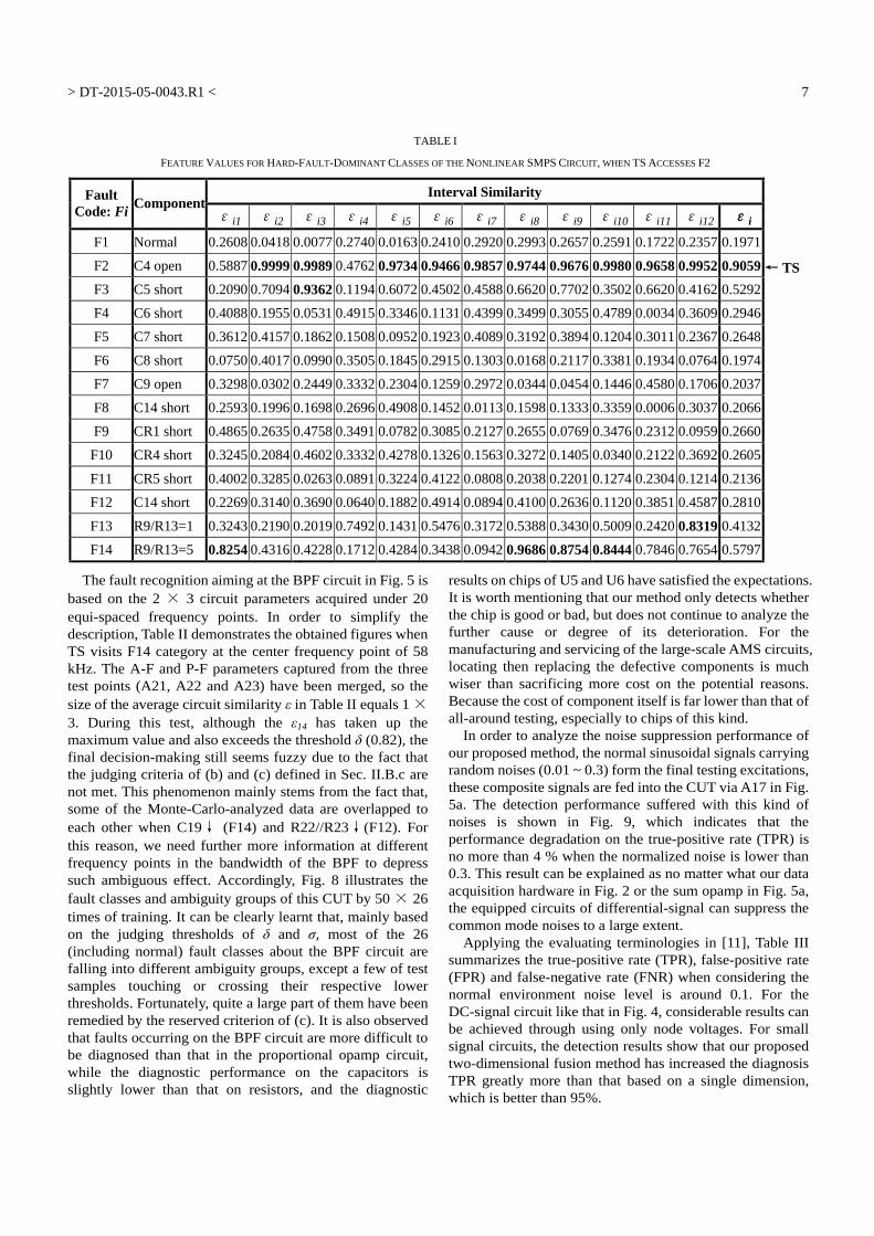
diagnosis of the pure analog circuit in Fig. 4 and the AMS circuit in Fig. 5. The data in Table I are randomly sampled by our AFDD system when a certain fault (C4 open) occurs on the SMPS circuit. It is observed that the average circuit similarity ε2 of the TS to the feature interval FI2 based on the 12 circuit parameters ranks first, being bigger than the threshold δ (0.82), and there is a safe distance between the threshold σ (0.18) and the difference (0.3262) of εmax1 and εmax2, which mean this fault can uniquely be identified. The false touches to the threshold δ which are emphasized with bold fonts appear occasionally under some certain circuit parameters, nevertheless, the final decision-making will not be affected owing to the 12-circuit-parameter fusion. The fault classes and ambiguity groups of SMPS circuit in Fig. 4 are illustrated in Fig. 7, which were obtained by 50 × 14 times of Monte-Carlo analysis for each fault. These results show that nearly all the 14 (including normal) fault classes in the SMPS circuit are falling into different ambiguity groups, and thus, the true-positive rate (TPR) about this CUT is close to 100%. We have been continuously verifying this figure on our actual platform for more than half a year.
+20 dBOpamp
8×12Crosspoint
Switch
U32
Digital Control Signals 10
ANT1_TOP
Calibrate Signal
SumOpamp
SumOpamp
Band-passAPF
Band-passAPF
Buffer
Buffer
Gain 0/20dBOpamp
Gain 0/20dBOpamp
Band-passAPF
Band-passAPF
Gain 10/20dBOpamp
Gain 10/20dBOpamp
RX_CHAN1
RX_CHAN4
ANT1_BOT
+20 dBOpamp
ANT4_TOP
ANT4_BOT
(a)
(b)
A17
+3.3V +5V
C16.1U
GND
R34
2.49K
R15 1K
C15.1U
R212.74K
A24
C17100P
R17499
R14 1K
R18 11.5K
C23 33P
C18100P
R32 2.49K A24
CHAN4_PRE RX_CHAN4
GAIN_SET4_PRE
GAIN_SET4_POST
_________________________________Bandpass Filter__________________________ Gain = 10/20 dB+5V
+3.3V
+1.6V_BIAS
+3.3V
Gain = 0/20 dB
A25A22
R30 3.09K
R24 2.94K
R223.09K
R232.94K
A23
R28 3.09K
R27 2.94K
R253.09K
R262.94K
C271800P
C21 33P
-
+U7A
TS974IPT
2
31
411
Gain = 0 dB
C26.1U
+1.6V_BIAS
R332.49K
R20499
CR7MMBD4448
1 2
3
-
+
U6B
TS974IPT
6
57
C281800P
U5
SN74LVC1G3157
B21
S6 B1
3
GND2
VCC5
A4
R362.49K+
-U6D
TS974IPT
13
1214
A22
R35 8.87K
R31 24.9K
CR8
MMBD4448
1 2
3
C22 33P
R191K
R161K
-
+
U7B
TS974IPT6
57
+
-U7C
TS974IPT
9
108
R29 24.9K
C19 1800P+1.6V_BIAS
R37 8.87K
GND
GND
GND GND
GND
GND-
+U6A
TS974IPT
2
31
411
C25.1U
U8A
DG412L
1
2 3
4 51312
C20 1800P
+
-U6C
TS974IPT
9
108
A25
A21
A23
A20
A20
D33
D34
A21
…… … … … … … … …
…
Fig. 5. Example 2: The quad-opamp 4th order BPF circuit used in this paper. (a) Receiver circuit structure, and (b) Meta-circuit for case study.
> DT-2015-05-0043.R1 <
7
The fault recognition aiming at the BPF circuit in Fig. 5 is based on the 2 × 3 circuit parameters acquired under 20 equi-spaced frequency points. In order to simplify the description, Table II demonstrates the obtained figures when TS visits F14 category at the center frequency point of 58 kHz. The A-F and P-F parameters captured from the three test points (A21, A22 and A23) have been merged, so the size of the average circuit similarity ε in Table II equals 1 × 3. During this test, although the ε14 has taken up the maximum value and also exceeds the threshold δ (0.82), the final decision-making still seems fuzzy due to the fact that the judging criteria of (b) and (c) defined in Sec. II.B.c are not met. This phenomenon mainly stems from the fact that, some of the Monte-Carlo-analyzed data are overlapped to each other when C19↓ (F14) and R22//R23↓(F12). For this reason, we need further more information at different frequency points in the bandwidth of the BPF to depress such ambiguous effect. Accordingly, Fig. 8 illustrates the fault classes and ambiguity groups of this CUT by 50 × 26 times of training. It can be clearly learnt that, mainly based on the judging thresholds of δ and σ, most of the 26 (including normal) fault classes about the BPF circuit are falling into different ambiguity groups, except a few of test samples touching or crossing their respective lower thresholds. Fortunately, quite a large part of them have been remedied by the reserved criterion of (c). It is also observed that faults occurring on the BPF circuit are more difficult to be diagnosed than that in the proportional opamp circuit, while the diagnostic performance on the capacitors is slightly lower than that on resistors, and the diagnostic
results on chips of U5 and U6 have satisfied the expectations. It is worth mentioning that our method only detects whether the chip is good or bad, but does not continue to analyze the further cause or degree of its deterioration. For the manufacturing and servicing of the large-scale AMS circuits, locating then replacing the defective components is much wiser than sacrificing more cost on the potential reasons. Because the cost of component itself is far lower than that of all-around testing, especially to chips of this kind.
In order to analyze the noise suppression performance of our proposed method, the normal sinusoidal signals carrying random noises (0.01 ~ 0.3) form the final testing excitations, these composite signals are fed into the CUT via A17 in Fig. 5a. The detection performance suffered with this kind of noises is shown in Fig. 9, which indicates that the performance degradation on the true-positive rate (TPR) is no more than 4 % when the normalized noise is lower than 0.3. This result can be explained as no matter what our data acquisition hardware in Fig. 2 or the sum opamp in Fig. 5a, the equipped circuits of differential-signal can suppress the common mode noises to a large extent.
Applying the evaluating terminologies in [11], Table III summarizes the true-positive rate (TPR), false-positive rate (FPR) and false-negative rate (FNR) when considering the normal environment noise level is around 0.1. For the DC-signal circuit like that in Fig. 4, considerable results can be achieved through using only node voltages. For small signal circuits, the detection results show that our proposed two-dimensional fusion method has increased the diagnosis TPR greatly more than that based on a single dimension, which is better than 95%.
TABLE I
FEATURE VALUES FOR HARD-FAULT-DOMINANT CLASSES OF THE NONLINEAR SMPS CIRCUIT, WHEN TS ACCESSES F2
Interval Similarity Fault Code: Fi Component
εi1 εi2 εi3 εi4 εi5 εi6 εi7 εi8 εi9 εi10 εi11 εi12 εi
F1 Normal 0.2608 0.0418 0.0077 0.2740 0.0163 0.2410 0.2920 0.2993 0.2657 0.2591 0.1722 0.2357 0.1971 F2 C4 open 0.5887 0.9999 0.9989 0.4762 0.9734 0.9466 0.9857 0.9744 0.9676 0.9980 0.9658 0.9952 0.9059 ← TS
F3 C5 short 0.2090 0.7094 0.9362 0.1194 0.6072 0.4502 0.4588 0.6620 0.7702 0.3502 0.6620 0.4162 0.5292 F4 C6 short 0.4088 0.1955 0.0531 0.4915 0.3346 0.1131 0.4399 0.3499 0.3055 0.4789 0.0034 0.3609 0.2946 F5 C7 short 0.3612 0.4157 0.1862 0.1508 0.0952 0.1923 0.4089 0.3192 0.3894 0.1204 0.3011 0.2367 0.2648 F6 C8 short 0.0750 0.4017 0.0990 0.3505 0.1845 0.2915 0.1303 0.0168 0.2117 0.3381 0.1934 0.0764 0.1974 F7 C9 open 0.3298 0.0302 0.2449 0.3332 0.2304 0.1259 0.2972 0.0344 0.0454 0.1446 0.4580 0.1706 0.2037 F8 C14 short 0.2593 0.1996 0.1698 0.2696 0.4908 0.1452 0.0113 0.1598 0.1333 0.3359 0.0006 0.3037 0.2066 F9 CR1 short 0.4865 0.2635 0.4758 0.3491 0.0782 0.3085 0.2127 0.2655 0.0769 0.3476 0.2312 0.0959 0.2660
F10 CR4 short 0.3245 0.2084 0.4602 0.3332 0.4278 0.1326 0.1563 0.3272 0.1405 0.0340 0.2122 0.3692 0.2605 F11 CR5 short 0.4002 0.3285 0.0263 0.0891 0.3224 0.4122 0.0808 0.2038 0.2201 0.1274 0.2304 0.1214 0.2136 F12 C14 short 0.2269 0.3140 0.3690 0.0640 0.1882 0.4914 0.0894 0.4100 0.2636 0.1120 0.3851 0.4587 0.2810 F13 R9/R13=1 0.3243 0.2190 0.2019 0.7492 0.1431 0.5476 0.3172 0.5388 0.3430 0.5009 0.2420 0.8319 0.4132 F14 R9/R13=5 0.8254 0.4316 0.4228 0.1712 0.4284 0.3438 0.0942 0.9686 0.8754 0.8444 0.7846 0.7654 0.5797

> DT-2015-05-0043.R1 <
8
In addition, the integration level of the DC-signal-circuit (e.g. CUT in Fig. 4) is always slightly lower than that of the small-signal-circuit (e.g. CUT in Fig. 5), so the former kind
of circuit can move more PCB areas for placing test points (accessible nodes), which explains why the parameter totality in Table I equals 12 while that in Table II is only 3.
TABLE II
FEATURE VALUES FOR SOFT-FAULT-DOMINANT CLASSES OF THE BPF CIRCUIT, CAPTURED AT 58 KHZ FREQUENCY POINT, WHEN TS ACCESSES F16
Interval Similarity Interval Similarity Fault Code: Fi Component
εi1 εi2 εi3 εi
Fault Code: Fi Component
εi1 εi2 εi3 εi
F1 R34↑ 0.0184 0.2477 0.2716 0.1792 F14 C19↓ 0.5909 0.8902 0.9982 0.8264 ← TS F2 R34↓ 0.0542 0.1307 0.3019 0.1623 F15 C28↑ 0.1824 0.1462 0.2668 0.1985 F3 R21↑ 0.0397 0.2185 0.0423 0.1002 F16 C28↓ 0.1618 0.0115 0.3198 0.1644 F4 R21↓ 0.1661 0.0571 0.3045 0.1759 F17 R24//R30↑ 0.0498 0.2552 0.1406 0.1485 F5 R29↑ 0.0108 0.2353 0.3199 0.1887 F18 R24//R30↓ 0.0858 0.2651 0.3052 0.2187 F6 R29↓ 0.0325 0.0106 0.1135 0.0522 F19 R15↑ 0.1802 0.0623 0.2641 0.1689 F7 C21↑ 0.0928 0.0923 0.1951 0.1267 F20 R15↓ 0.0848 0.1633 0.3198 0.1893 F8 C21↓ 0.0746 0.0154 0.1823 0.0908 F21 R19↑ 0.0186 0.1485 0.2714 0.1462 F9 R37↑ 0.0505 0.0314 0.3192 0.1337 F22 R19↓ 0.0119 0.2154 0.0812 0.1028 F10 R37↓ 0.0851 0.2745 0.3216 0.2271 F23 CR7 Pin1S3 0.0830 0.2365 0.3098 0.2098 F11 R22//R23↑ 0.0525 0.2316 0.1687 0.1509 F24 U5 Broken 0.0107 0.2516 0.3113 0.1912 F12 R22//R23↓ 0.4551 0.8235 0.9649 0.7478 F25 U6 Broken 0.0655 0.0920 0.2262 0.1279 F13 C19↑ 0.0330 0.1057 0.3235 0.1541 F26 Normal 0.0837 0.2266 0.2526 0.1876
Fig. 7. Fault classes for SMPS circuit in Fig. 4. Fig. 9. Performance degradation on the true-positive rate (TPR).
Fig. 8. Fault classes for BPF circuit in Fig. 5.
> DT-2015-05-0043.R1 <
9
Such distinguishing method of parameter selection according to different features of circuits possesses higher adaptability for fault diagnosis on VLSI circuits.
B. Performance evaluation
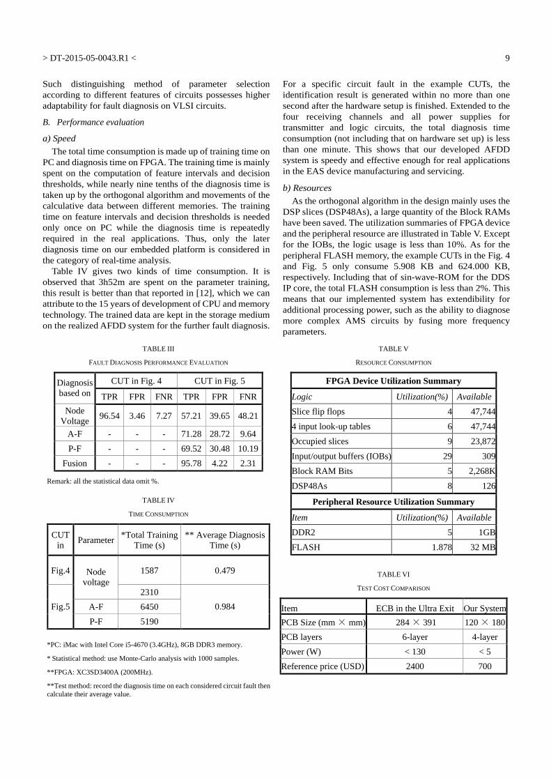
a) Speed The total time consumption is made up of training time on
PC and diagnosis time on FPGA. The training time is mainly spent on the computation of feature intervals and decision thresholds, while nearly nine tenths of the diagnosis time is taken up by the orthogonal algorithm and movements of the calculative data between different memories. The training time on feature intervals and decision thresholds is needed only once on PC while the diagnosis time is repeatedly required in the real applications. Thus, only the later diagnosis time on our embedded platform is considered in the category of real-time analysis.
Table IV gives two kinds of time consumption. It is observed that 3h52m are spent on the parameter training, this result is better than that reported in [12], which we can attribute to the 15 years of development of CPU and memory technology. The trained data are kept in the storage medium on the realized AFDD system for the further fault diagnosis.
For a specific circuit fault in the example CUTs, the identification result is generated within no more than one second after the hardware setup is finished. Extended to the four receiving channels and all power supplies for transmitter and logic circuits, the total diagnosis time consumption (not including that on hardware set up) is less than one minute. This shows that our developed AFDD system is speedy and effective enough for real applications in the EAS device manufacturing and servicing.
b) Resources As the orthogonal algorithm in the design mainly uses the
DSP slices (DSP48As), a large quantity of the Block RAMs have been saved. The utilization summaries of FPGA device and the peripheral resource are illustrated in Table V. Except for the IOBs, the logic usage is less than 10%. As for the peripheral FLASH memory, the example CUTs in the Fig. 4 and Fig. 5 only consume 5.908 KB and 624.000 KB, respectively. Including that of sin-wave-ROM for the DDS IP core, the total FLASH consumption is less than 2%. This means that our implemented system has extendibility for additional processing power, such as the ability to diagnose more complex AMS circuits by fusing more frequency parameters.
TABLE III
FAULT DIAGNOSIS PERFORMANCE EVALUATION
CUT in Fig. 4 CUT in Fig. 5 Diagnosis based on TPR FPR FNR TPR FPR FNR
Node Voltage 96.54 3.46 7.27 57.21 39.65 48.21
A-F - - - 71.28 28.72 9.64 P-F - - - 69.52 30.48 10.19
Fusion - - - 95.78 4.22 2.31
Remark: all the statistical data omit %.
TABLE V
RESOURCE CONSUMPTION
FPGA Device Utilization Summary
Logic Utilization(%) Available Slice flip flops 4 47,744
4 input look-up tables 6 47,744
Occupied slices 9 23,872
Input/output buffers (IOBs) 29 309
Block RAM Bits 5 2,268K
DSP48As 8 126
Peripheral Resource Utilization Summary
Item Utilization(%) Available DDR2 5 1GB
FLASH 1.878 32 MB
TABLE IV
TIME CONSUMPTION
CUT in Parameter *Total Training
Time (s) ** Average Diagnosis
Time (s)
Fig.4 1587 0.479 Node voltage
2310 A-F 6450 Fig.5
P-F 5190
0.984
*PC: iMac with Intel Core i5-4670 (3.4GHz), 8GB DDR3 memory.
* Statistical method: use Monte-Carlo analysis with 1000 samples.
**FPGA: XC3SD3400A (200MHz).
**Test method: record the diagnosis time on each considered circuit fault then calculate their average value.
TABLE VI
TEST COST COMPARISON
Item ECB in the Ultra Exit Our SystemPCB Size (mm × mm) 284 × 391 120 × 180 PCB layers 6-layer 4-layer Power (W) < 130 < 5 Reference price (USD) 2400 700

> DT-2015-05-0043.R1 <
10
c) Test cost At present, the frequently-used fault diagnosis method for
the AM-EAS devices is based on several instruments including but not limited to arbitrary waveform generator (AWG), oscilloscope (OSC) and high voltage differential probe (HV-DP). In accordance with the requirements of bandwidth, accuracy and channel for an average EAS device, only the instruments would cost more than 3000 USD. Moreover, most of the EAS distributors who are the main liable maintenance deployments to the end retail customers are not familiar with such professional instruments. If there was a smart detection system that can diagnose the AMS fault in real time, this test cost would be dramatically reduced. The detailed cost comparison between the ECB under test and our diagnosis system has been summarized in Table VI. Compared to that in [11], our experimental setup is more compact and practicable to scale to the realistic applications. All of these show promise for the proposed simple detection and diagnosis system to solve the complex AMS circuit faults problems.
VI. CONCLUSION This paper has developed a cost-effective fault detection
and diagnosis system for AM-EAS devices based on FPGA. The offered abundant acquisition channels are in charge of gathering the circuit parameters of node voltage, amplitude and phase responding to the programmable signal excitations. Test results show that the interval-math-based diagnostic method has three obvious advantages, i.e. resource-saving, fast detecting speed, and balanced statistical rates among TPR, FPR and FNR.
However, because Monte-Carlo simulation is relatively time consuming, we have to spend a fair chunk of time on the training of the feature intervals and the decision thresholds on PC, which are just closely related to the AFDD system's detecting performance. Future research will focus on making the training method more time-saving and the embedded algorithm more efficient, with the goal of portable diagnostic equipment that could stand ready for widespread adoption in the EAS industry.
REFERENCES [1] Y. He, Y.H. Tan and Y. Sun, “A neural network approach for fault
diagnosis of large-scale analogue circuits,” in IEEE Int. Symp. on Circuits and Systems (ISCAS), May 2002, vol.1, pp.I-153-I-156.
[2] P. Wang and S.Y. Yang, “A new diagnosis approach for handling tolerance in analog and mixed-signal circuits by using fuzzy math,” IEEE Trans. Circuits Syst. I, Reg. Papers, vol.52, no.10, pp.2118-2127, Oct. 2005.
[3] V. Stopjakova et al., “Defect detection in analog and mixed circuits by neural networks using wavelet analysis,” IEEE Trans. Rel., vol.54, no.3, pp. 441-448, Sep. 2005.
[4] P.N. Variyam, S. Cherubal and A. Chatterjee, “Prediction of analog performance parameters using fast transient testing,” IEEE Trans. Comput.-Aided Design Integr. Circuits Syst., vol. 21, no. 3, pp. 349-361, Aug. 2002.
[5] Q. Yang, Y.Y. Zhu and F. Wu, “Remote Intelligent Fault Diagnosis of Analog Circuit,” IEEE Int. Conf. on Natural Comput. (ICNC), Shanghai, China, Jul. 2011, vol. 3, pp. 1677-1680.
[6] G. Kang and Om P. Gandhi, “Comparison of various safety guidelines for electronic article surveillance devices with pulsed magnetic fields,” IEEE Trans. Biomed. Engineering, vol. 50, no. 1, pp. 107-113, Jan. 2003.
[7] E. Bottani et al., “Performances of RFID, acousto-magnetic and radio frequency technologies for electronic article surveillance in the apparel industry in Europe: A quantitative study,” I. J. RF Technol.: Res. and Appl., vol. 3, no. 2, pp. 137-158, 2012.
[8] M.F. Peng, Y. He and Y. Sun, “Analog circuit diagnosis using RBF network and D-S evidential reasoning,” Trans. of China Electrotechnical Society, vol. 24, no.8, pp. 6-13, Aug. 2009.
[9] M.F. Peng Y. He and J.X. Lv, “Fault location of analog circuits using intelligent information fusion technology (IN CHINESE),” Trans. of China Electrotechnical Society, vol. 20, no. 11, pp. 93-96, Nov. 2005.
[10] L. F. Yuan, Y. He and Y. Sun, “A new neural-network-based fault diagnosis approach for analog circuits by using kurtosis and entropy as a preprocessor,” IEEE Trans. Instrum. Meas., vol. 59, no. 3, pp. 586 - 595, Mar. 2010.
[11] A. S. Sarathi Vasan, B. Long and M. Pecht, “Diagnostics and prognostics method for analog electronic circuits,” IEEE Trans. Ind. Electron., vol. 60, no. 11, pp. 5277-5291, Nov. 2013.
[12] A. Abderrahman, E. Cerny and B. Kaminska, “Worst Case Tolerance Analysis and CLP-Based Multifrequency Test Generation for Analog Circuits,” IEEE Trans. Comput.-Aided Design Integr. Circuits Syst., vol. 18, no. 3, pp. 332-345, Mar. 1999.
Qiwu Luo received his M.S. degree in Electronic Science and Technology in 2011 and is currently pursuing his Ph.D. degree in Electrical Engineering from Hunan University, Changsha, China. His current interests include the research of fault testing and diagnosis of large-scale analog circuits, intelligent and real-time information processing. Contact Infor: Room 619, Research Building, College of Electrical and Information Engineering, Hunan University, Yue Lu District, Changsha, Hunan, China. Tel: +86(0)731 88822252, Fax: +86(0)731 88822224, E-mail: [email protected] Yigang He is currently a professor of Electrical Engineering at Hefei University of Technology, Hefei, China. He received his Ph.D. degree in electrical engineering from Xi’an Jiaotong University, Xi’an, China, in 1996. His research interests include testing and fault diagnosis of analog and mixed-signal circuits, intelligent signal processing and RFID. Contact Infor: Floor 11, Yifu Building, School of Electrical and Automation Engineering, Hefei University of Technology, Hefei, Anhui, China. Tel: +86(0)551 62904435, Fax: +86(0)551 62901408, E-mail: [email protected] Yichuang Sun is currently a professor of Communications Electronics at University of Hertfordshire, UK. He received his Ph.D. degree from University of York, U.K. His research interests are integrated RF and mixed-signal circuits, software defined radio transceivers, and wireless and mobile communication systems. He is a Senior Member of IEEE. Contact Infor: School of Engineering and Technology, University of Hertfordshire, Hatfield ALl0 9AB, Hertfordshire, United Kingdom. Tel: +44(0)1707 284196, Fax: +44(0)1707 284199, E-mail: [email protected]