research article electrical properties of amorphous...
TRANSCRIPT
Hindawi Publishing CorporationAdvances in Condensed Matter PhysicsVolume 2013, Article ID 365475, 5 pageshttp://dx.doi.org/10.1155/2013/365475
Research ArticleElectrical Properties of Amorphous Titanium OxideThin Films for Bolometric Application
Yongfeng Ju, Mahua Wang, Yunlong Wang, Shihu Wang, and Chengfang Fu
Faculty of Electronic and Electrical Engineering, Huaiyin Institute of Technology, Huaian 223003, China
Correspondence should be addressed to Yongfeng Ju; yfju [email protected]
Received 1 August 2013; Accepted 15 October 2013
Academic Editor: Xia Xiang
Copyright © 2013 Yongfeng Ju et al. This is an open access article distributed under the Creative Commons Attribution License,which permits unrestricted use, distribution, and reproduction in any medium, provided the original work is properly cited.
We report the electrical conduction mechanism of amorphous titanium oxide thin films applied for bolometers. As the O/Ti ratiovaries from 1.73 to 1.97 measured by rutherford backscattering spectroscopy, the resistivity of the films increases from 0.26Ω cmto 10.1Ω cm. At the same time, the temperature coefficient of resistivity and activation energy vary from −1.2% to −2.3% andfrom 0.09 eV to 0.18 eV, respectively. The temperature dependence of the electrical conductivity illustrates a thermally activatedconduction behavior and the carrier transport mechanism in the titanium oxide thin films is found to obey the normal Meyer-Neldel Rule in the temperature range from 293K to 373K.
1. Introduction
Titanium dioxide (TiO2) is one of the most widely studied
transition metal oxide semiconductors due to its nontoxicnature, chemical stability, and commercial availability at alow cost, robust, and general reactivity. During the pastdecades, TiO
2thin films have attractedmuch interest because
it has a wide range of promising energy and environmentalapplications, such as hydrogen generation by water splitting[1], photocatalytic water purification [2], dye-sensitized solarcells [3], and gas sensors [4]. Recently, few people havefabricated amorphous nonstoichiometric titanium dioxide,(a-TiO
𝑥, where 𝑥 is smaller than 2) thin films by different
methods and pointed out that a-TiO𝑥thin films are potential
thermal sensing material for an uncooled IR bolometerimager [5]. However, the effect of the deposition processon the film structure, composition and electrical propertiesof this material such as resistivity, temperature coefficientof resistivity (TCR), and activation energy, have not beenillustrated up to now, and these factors are very crucial forthe detectivity of thermal IR detectors.
TiO𝑥thin films can be prepared by sol-gel [6], hydrother-
mal [7], chemical and physical vapor deposition [8]. Reactivesputtering is a commonly used physical vapor depositionmethod to grow dense and uniform metal oxide films for
industrial application [9, 10]. In this process, a metal target issputtered in an atmosphere consisting of argon and oxygen,this allows higher deposition rates than does the sputteringof an oxide target [10]. It has been experimentally establishedthat the oxygen partial pressure (pO
2) during sputtering has
the most significant effect on the structure, phase composi-tion, and electrical properties of TiO
𝑥thin films [11].
TiO2is electrically insulating with an extremely high
resistivity above 108Ω cm, but the suboxidized TiO2with an
excess of titanium is an n type semiconductor with uniqueproperties [12], indicating the defect disorder and O/Ti stoi-chiometry play an important role in the electrical propertiesof TiO
𝑥[13]. In this work, we have mainly investigated the
electrical properties and electron transport mechanism of a-TiO𝑥thin films applied for uncooled IR thermal detectors.
2. Experimental
TiO𝑥thin films were deposited on K9 glass and p-silicon
(100) substrates simultaneously at room temperature by adc reactive sputtering technique. Oxygen and argon wereused as reactive gas and sputtering gas, respectively. Thetotal pressure was kept at 1 Pa and the other characteristicparameters of the investigated samples are summarized inTable 1.

2 Advances in Condensed Matter Physics
Table 1: Experimental parameters of reactive sputtering and the results of measurements. (SCCM is an abbreviation of standard cubiccentimeter per minute).
Samples Ar (SCCM) O2/(O2+ Ar)(pO2)
Thickness 𝑑(nm) O/Ti ratio Resistivity 𝜌
(Ω cm)Conductivity𝜎 (Ω−1 cm−1)
Activationenergy 𝐸
𝑎(eV) |TCR| (%)
S10 80 1.0% 101 1.73 0.26 3.85 0.09 1.2S25 80 2.5% 100 1.84 1.9 0.53 0.15 1.9S40 80 4.0% 98 1.91 3.1 0.32 0.16 2.0S55 80 5.5% 99 1.97 10.1 0.01 0.18 2.3
20 30 40 50 60 70 80
Inte
nsity
(a.u
.)
S25
2𝜃 (∘)
Figure 1: XRD pattern of TiO𝑥thin film (S25) deposited at the pO
2
of 1.5%.
The thickness and surface morphology of the films werecharacterized by field emission scanning electronmicroscopy(FESEM, Hitachi S4800). Glancing incidence X-ray diffrac-tion (GIXRD, PANalytical X’Pert PRO) was performed byusing Cu𝐾𝛼 radiation (0.1564 nm) with a glancing incidenceof 2∘, 𝑈 = 40 kV and 𝐼 = 35mA. The O/Ti stoichiom-etry of the films was measured by rutherford backscatter-ing spectrometry (RBS, NEC 5SDH-2) performed with a2.023MeV 4He+ beam from a 2 × 1.7MV tandem accelerator.The temperature dependent electrical measurements wereperformed with a semiconductor characterization system(Keithley, 4200-SCS) in a temperature controller (SigmaSystems, Sigma C4) with an accuracy of 0.1∘.
3. Results and Discussion
The GIXRD pattern for sample S25 is shown in Figure 1. Thepatterns of the other three samples have similar characteris-tics as S25. No sharp diffraction peak of any crystalline phaseis observed, which indicates all the films deposited at roomtemperature have amorphous structure, with no preferredorientation as demonstrated in the previous studies [5, 14, 15].
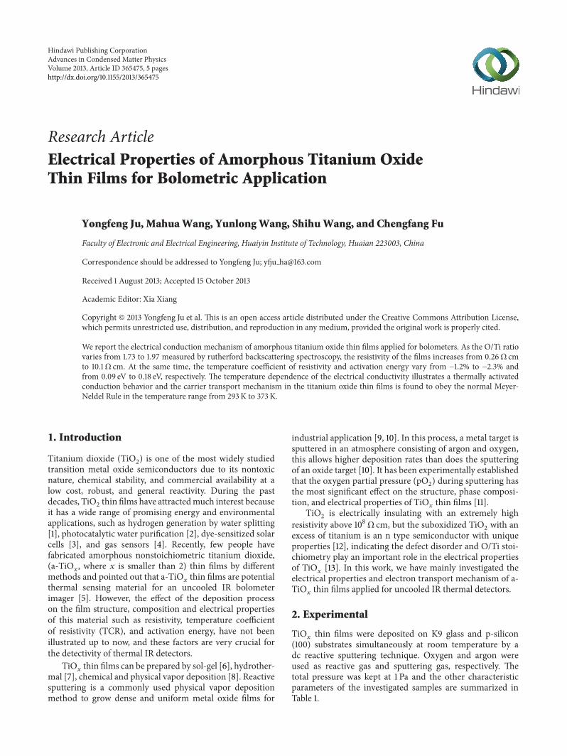
Figure 2 presents the cross-sectional and surface mor-phological micrographs of sample S25, which shows that thethickness of the TiO
𝑥film is about 100 nm, and the film
is dense and smooth, which is the advantage of sputteringtechnique compared with other deposition methods [10].
Furthermore, no grain or cluster appears in the films, thisconfirms the amorphous structure of the films.
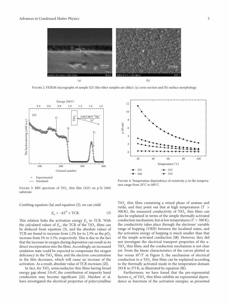
Figure 3 shows a typical experimental RBS spectrumof titanium oxide films (S25) deposited on p-silicon (100)substrate with the simulated spectrum using the programSIMNRA [16]. The O/Ti stoichiometry across the films havebeen obtained by simulating the experimental spectrum(circle) and theoretical spectrum (line).The results presentedin Table 1 show the O/Ti ratio is in accordance with the pO
2,
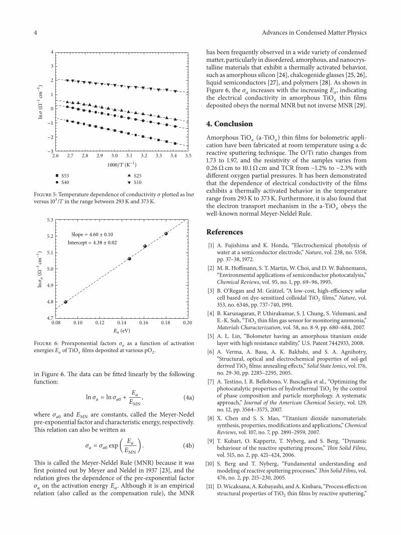
and all the films have nonstoichiometry compositions.Figure 4 shows the electrical resistivity (𝜌) of TiO
𝑥films
as a function of temperature. As is seen, the resistivityis significantly influenced by the pO
2during the deposi-
tion process. The resistivity measured at room temperatureincreases from 0.26Ω cm to 10.1Ω cm as the pO
2increases
from 1% to 5.5%. This can be explained by the decrease ofoxygen vacancies in the TiO
𝑥films with the increasing pO
2
[17], resulting in an increase of O/Ti ratio as illustrated byRBS analysis. Thus the larger resistivity is obtained [12]. Theelectrical resistivity (𝜌) or conductivity (𝜎) of the broad-bandsemiconductors can be expressed as follows [18]:
𝜌 = 𝜌𝑎exp(𝐸𝑎
𝑘𝑇) , (1a)
𝜎 = 𝜎𝑎exp(−𝐸𝑎
𝑘𝑇) , (1b)
where 𝐸𝑎is the thermal activation energy, 𝑘 is the Boltzmann
constant, 𝑇 is the absolute temperature, and the preexpo-nential factors 𝜌
𝑎and 𝜎
𝑎are the resistivity at 𝑇 → ∞
and conductivity at 𝑇 → 0, respectively. As can be seenin Figure 4, the curves exhibit Arrhenius characteristics inaccordance with equation (1a) [19].
From the temperature dependence of electrical conduc-tivity plotted as ln𝜎 versus 103/𝑇 shown in Figure 5, theactivation energies of TiO
𝑥films can be calculated from the
slopes of the fitted lines by equation (1b), and the results arepresented in Table 1 show that the activation energy increasesfrom 0.09 eV to 0.18 eV with the increasing resistivity. Withthe activation energies, the temperature coefficient of resistiv-ity (TCR) can be obtained and TCR is extensively exploitedas one of the most important parameters characterizing thedetectivity of uncooled IR sensors, defined as the slope ofnatural logarithm resistivity [20]:
TCR = (1𝜌) × (𝑑𝜌
𝑑𝑇) . (2)
Advances in Condensed Matter Physics 3
Glass
TiOx
100 nm
(a)
100 nm
(b)
Figure 2: FESEMmicrographs of sample S25 (the other samples are alike): (a) cross-section and (b) surface morphology.
100 200 300 400
O
The b
acks
catte
ring
yiel
d (a
.u.)
Channel number
ExperimentalSimulated
TiSi
Energy (MeV)
S25
0.4 0.6 0.8 1.0 1.2 1.4 1.6
15∘TiOx 2.023MeV 4He+
Figure 3: RBS spectrum of TiO𝑥thin film (S25) on p-Si (100)
substrate.
Combing equation (1a) and equation (2), we can yield
𝐸𝑎= −𝑘𝑇
2× TCR. (3)
This relation links the activation energy 𝐸𝑎to TCR. With
the calculated values of 𝐸𝑎, the TCR of the TiO
𝑥films can
be deduced from equation (3), and the absolute values ofTCR are found to increase from 1.2% for to 2.3% as the pO
2
increase from 1% to 5.5%, respectively. This is due to the factthat the increase in oxygen during deposition can result in itsdirect incorporation into the films. Accordingly, an increasedoxidation state could be expected to compensate the oxygendeficiency in the TiO
𝑥films, and the electron concentration
in the film decreases, which will cause an increase of theactivation. As a result, absolute value of TCR increases [21].
In fact, for TiO2semiconductor thin films having broad
energy gap about 3.0 eV, the contribution of impurity bandconduction may become significant [22]. Mardare et al.have investigated the electrical properties of polycrystalline
20 40 60 80 100
0
2
4
6
8
10
12
S55S40
S25S10
Temperature (∘C)
𝜌(Ω
cm)
Figure 4: Temperature dependence of resistivity 𝜌 in the tempera-ture range from 20∘C to 100∘C.
TiO𝑥thin films containing a mixed phase of anatase and
rutile, and they point out that at high temperatures (𝑇 >300K), the measured conductivity of TiO
𝑥thin films can
also be explained in terms of the simple thermally activatedconductionmechanism, but at low temperatures (𝑇 < 300K),the conductivity takes place through the electrons’ variablerange of hopping (VRH) between the localized states, andthe activation energy of hopping is much smaller than thatof the simple activated conduction [18]. However, they didnot investigate the electrical transport properties of the a-TiO𝑥thin films, and the conduction mechanism is not clear
yet. From the linear characteristics of the curves plotted asln𝜎 versus 103/𝑇 in Figure 5, the mechanism of electricalconduction in a-TiO
𝑥thin films can be explained according
to the thermally activated mode in the temperature domain293K to 373K, as illustrated by equation (1b).
Furthermore, we have found that the pre-exponentialfactors 𝜎
𝑎of TiO
𝑥thin films exhibits an exponential depen-
dence as functions of the activation energies, as presented
4 Advances in Condensed Matter Physics
2.6 2.7 2.8 2.9 3.0 3.1 3.2 3.3 3.4 3.5
0
1
2
3
4
S55S40
S25S10
1000/T (K−1)
ln𝜎
(Ω−1
cm−1)
−3
−2
−1
Figure 5: Temperature dependence of conductivity 𝜎 plotted as ln𝜎versus 103/𝑇 in the range between 293K and 373K.
0.08 0.10 0.12 0.14 0.16 0.18 0.204.7
4.8
4.9
5.0
5.1
5.2
5.3
Slope = 4.60 ± 0.10
Intercept = 4.38 ± 0.02
ln𝜎a
(Ω−1
cm−1)
Ea (eV)
Figure 6: Preexponential factors 𝜎𝑎as a function of activation
energies 𝐸𝑎of TiO
𝑥films deposited at various pO
2.
in Figure 6. The data can be fitted linearly by the followingfunction:
ln𝜎𝑎= ln𝜎
𝑎0+𝐸𝑎
𝐸MN, (4a)
where 𝜎𝑎0
and 𝐸MN are constants, called the Meyer-Nedelpre-exponential factor and characteristic energy, respectively.This relation can also be written as
𝜎𝑎= 𝜎𝑎0exp(𝐸𝑎
𝐸MN) . (4b)
This is called the Meyer-Neldel Rule (MNR) because it wasfirst pointed out by Meyer and Neldel in 1937 [23], and therelation gives the dependence of the pre-exponential factor𝜎𝑎on the activation energy 𝐸
𝑎. Although it is an empirical
relation (also called as the compensation rule), the MNR
has been frequently observed in a wide variety of condensedmatter, particularly in disordered, amorphous, and nanocrys-talline materials that exhibit a thermally activated behavior,such as amorphous silicon [24], chalcogenide glasses [25, 26],liquid semiconductors [27], and polymers [28]. As shown inFigure 6, the 𝜎
𝑎increases with the increasing 𝐸
𝑎, indicating
the electrical conductivity in amorphous TiO𝑥thin films
deposited obeys the normal MNR but not inverse MNR [29].
4. Conclusion
Amorphous TiO𝑥(a-TiO
𝑥) thin films for bolometric appli-
cation have been fabricated at room temperature using a dcreactive sputtering technique. The O/Ti ratio changes from1.73 to 1.97, and the resistivity of the samples varies from0.26Ω cm to 10.1Ω cm and TCR from −1.2% to −2.3% withdifferent oxygen partial pressures. It has been demonstratedthat the dependence of electrical conductivity of the filmsexhibits a thermally activated behavior in the temperaturerange from 293K to 373K. Furthermore, it is also found thatthe electron transport mechanism in the a-TiO
𝑥obeys the
well-known normal Meyer-Neldel Rule.
References
[1] A. Fujishima and K. Honda, “Electrochemical photolysis ofwater at a semiconductor electrode,” Nature, vol. 238, no. 5358,pp. 37–38, 1972.
[2] M. R. Hoffmann, S. T. Martin, W. Choi, and D. W. Bahnemann,“Environmental applications of semiconductor photocatalysis,”Chemical Reviews, vol. 95, no. 1, pp. 69–96, 1995.
[3] B. O’Regan and M. Gratzel, “A low-cost, high-efficiency solarcell based on dye-sensitized colloidal TiO
2films,” Nature, vol.
353, no. 6346, pp. 737–740, 1991.[4] B. Karunagaran, P. Uthirakumar, S. J. Chung, S. Velumani, and
E.-K. Suh, “TiO2thin film gas sensor formonitoring ammonia,”
Materials Characterization, vol. 58, no. 8-9, pp. 680–684, 2007.[5] A. L. Lin, “Bolometer having an amorphous titanium oxide
layer with high resistance stability,” U.S. Patent 7442933, 2008.[6] A. Verma, A. Basu, A. K. Bakhshi, and S. A. Agnihotry,
“Structural, optical and electrochemical properties of sol-gelderived TiO
2films: annealing effects,” Solid State Ionics, vol. 176,
no. 29-30, pp. 2285–2295, 2005.[7] A. Testino, I. R. Bellobono, V. Buscaglia et al., “Optimizing the
photocatalytic properties of hydrothermal TiO2by the control
of phase composition and particle morphology. A systematicapproach,” Journal of the American Chemical Society, vol. 129,no. 12, pp. 3564–3575, 2007.
[8] X. Chen and S. S. Mao, “Titanium dioxide nanomaterials:synthesis, properties, modifications and applications,”ChemicalReviews, vol. 107, no. 7, pp. 2891–2959, 2007.
[9] T. Kubart, O. Kappertz, T. Nyberg, and S. Berg, “Dynamicbehaviour of the reactive sputtering process,” Thin Solid Films,vol. 515, no. 2, pp. 421–424, 2006.
[10] S. Berg and T. Nyberg, “Fundamental understanding andmodeling of reactive sputtering processes,”Thin Solid Films, vol.476, no. 2, pp. 215–230, 2005.
[11] D.Wicaksana,A.Kobayashi, andA.Kinbara, “Process effects onstructural properties of TiO
2thin films by reactive sputtering,”

Advances in Condensed Matter Physics 5
Journal of Vacuum Science and Technology A, vol. 10, pp. 1479–1482, 1992.
[12] R. G. Breckenridge and W. R. Hosler, “Electrical properties oftitanium dioxide semiconductors,” Physical Review, vol. 91, no.4, pp. 793–802, 1953.
[13] J. Nowotny, T. Bak, M. K. Nowotny, and L. R. Sheppard,“Titanium dioxide for solar-hydrogen II. Defect chemistry,”International Journal of Hydrogen Energy, vol. 32, no. 14, pp.2630–2643, 2007.
[14] P. Lobl, M. Huppertz, andD.Mergel, “Nucleation and growth inTiO2films prepared by sputtering and evaporation,”Thin Solid
Films, vol. 251, no. 1, pp. 72–79, 1994.[15] L.-J. Meng, M. Andritschky, and M. P. dos Santos, “The effect
of substrate temperature on the properties of d.c. reactivemagnetron sputtered titanium oxide films,” Thin Solid Films,vol. 223, no. 2, pp. 242–247, 1993.
[16] M. Mayer, “SIMNRA, a simulation program for the analysis ofNRA, RBS and ERDA,” in AIP Conference Proceedings, vol. 475,pp. 541–544, 1999.
[17] L.-J. Meng and M. P. dos Santos, “The influence of oxygenpartial pressure on the properties of DC reactive magnetronsputtered titanium oxide films,”Applied Surface Science, vol. 68,no. 3, pp. 319–325, 1993.
[18] D.Mardare, C. Baban, R. Gavrila, M.Modreanu, andG. I. Rusu,“On the structure, morphology and electrical conductivities oftitanium oxide thin films,” Surface Science, vol. 507–510, pp.468–472, 2002.
[19] K. J. Laidler, “The development of the arrhenius equation,”Journal of Chemical Education, vol. 61, no. 6, pp. 494–498, 1984.
[20] K. C. Liddiard, “Thin-film resistance bolometer IR detectors,”Infrared Physics, vol. 24, no. 1, pp. 57–64, 1984.
[21] M. Soltani, M. Chaker, E. Haddad, R. V. Kruzelecky, and J.Margot, “Effects of Ti-W codoping on the optical and electricalswitching of vanadium dioxide thin films grown by a reactivepulsed laser deposition,” Applied Physics Letters, vol. 85, no. 11,pp. 1958–1960, 2004.
[22] M. Vaziri, “Low-temperature conductivity of epitaxial ZnSe inthe impurity band regime,” Applied Physics Letters, vol. 65, no.20, pp. 2568–2570, 1994.
[23] W. Meyer and H. Neldel, “A relation between the energyconstant 𝜀 and the quantity constant a in the conductivity-temperature formula for oxide,” Zeitschrift fur TechnischePhysik, vol. 18, pp. 588–593, 1937.
[24] R. S. Crandall, “Defect relaxation in amorphous silicon:stretched exponentials, theMeyer-Neldel rule, and the Staebler-Wronski effect,” Physical Review B, vol. 43, no. 5, pp. 4057–4070,1991.
[25] N. Mehta, “Meyer-Neldel rule in chalcogenide glasses: recentobservations and their consequences,” Current Opinion in SolidState and Materials Science, vol. 14, no. 5, pp. 95–106, 2010.
[26] K. Shimakawa and F. Abdel-Wahab, “The Meyer-Neldel rule inchalcogenide glasses,” Applied Physics Letters, vol. 70, no. 5, pp.652–654, 1997.
[27] J. Fortner, V. G. Karpov, and M.-L. Saboungi, “Meyer-Neldelrule for liquid semiconductors,” Applied Physics Letters, vol. 66,pp. 997–999, 1995.
[28] G. F. Myachina, T. G. Ermakova, and V. A. Lopyrev, “Com-pensation effect in the electric conduction in some conjugatedpolymers,” Physica Status Solidi A, vol. 81, no. 1, pp. 377–380,1984.
[29] K. L. Ngai, “Meyer-Neldel rule and anti Meyer-Neldel rule ofionic conductivity conclusions from the coupling model,” SolidState Ionics, vol. 105, no. 1–4, pp. 231–235, 1998.

Submit your manuscripts athttp://www.hindawi.com
Hindawi Publishing Corporationhttp://www.hindawi.com Volume 2014
High Energy PhysicsAdvances in
The Scientific World JournalHindawi Publishing Corporation http://www.hindawi.com Volume 2014
Hindawi Publishing Corporationhttp://www.hindawi.com Volume 2014
FluidsJournal of
Atomic and Molecular Physics
Journal of
Hindawi Publishing Corporationhttp://www.hindawi.com Volume 2014
Hindawi Publishing Corporationhttp://www.hindawi.com Volume 2014
Advances in Condensed Matter Physics
OpticsInternational Journal of
Hindawi Publishing Corporationhttp://www.hindawi.com Volume 2014
Hindawi Publishing Corporationhttp://www.hindawi.com Volume 2014
AstronomyAdvances in
International Journal of
Hindawi Publishing Corporationhttp://www.hindawi.com Volume 2014
Superconductivity
Hindawi Publishing Corporationhttp://www.hindawi.com Volume 2014
Statistical MechanicsInternational Journal of
Hindawi Publishing Corporationhttp://www.hindawi.com Volume 2014
GravityJournal of
Hindawi Publishing Corporationhttp://www.hindawi.com Volume 2014
AstrophysicsJournal of
Hindawi Publishing Corporationhttp://www.hindawi.com Volume 2014
Physics Research International
Hindawi Publishing Corporationhttp://www.hindawi.com Volume 2014
Solid State PhysicsJournal of
Computational Methods in Physics
Journal of
Hindawi Publishing Corporationhttp://www.hindawi.com Volume 2014
Hindawi Publishing Corporationhttp://www.hindawi.com Volume 2014
Soft MatterJournal of
Hindawi Publishing Corporationhttp://www.hindawi.com
AerodynamicsJournal of
Volume 2014
Hindawi Publishing Corporationhttp://www.hindawi.com Volume 2014
PhotonicsJournal of
Hindawi Publishing Corporationhttp://www.hindawi.com Volume 2014
Journal of
Biophysics
Hindawi Publishing Corporationhttp://www.hindawi.com Volume 2014
ThermodynamicsJournal of