research article experimental evaluation on the influence
TRANSCRIPT

Research ArticleExperimental Evaluation on the Influence of RCD Snubbers ina 3-Level Thyristor Based MLCR CSC
Bhaba P. Das,1 Neville R. Watson,2 and Yonghe Liu2,3
1The Engineering Department, ETEL Ltd., Auckland 0640, New Zealand2The Department of Electrical and Computer Engineering, University of Canterbury, Christchurch 8140, New Zealand3Inner Mongolia University of Technology, Hohhot, China
Correspondence should be addressed to Bhaba P. Das; [email protected]
Received 27 September 2015; Accepted 18 May 2016
Academic Editor: Jiun-Wei Horng
Copyright © 2016 Bhaba P. Das et al. This is an open access article distributed under the Creative Commons Attribution License,which permits unrestricted use, distribution, and reproduction in any medium, provided the original work is properly cited.
Multilevel current reinjection (MLCR) concept provides self-commutation capability to thyristors, enabling thyristor based currentsource converters (CSC) to operate under negative firing angle. It also lowers the input current harmonic distortion.This is achievedby using an auxiliary reinjection bridge. Extensive experimental results are presented in this paper to analyse the performance ofthe 3-level MLCR CSC for different snubber components across the reinjection bridge. The trade-off in the choice of the snubbercircuit is illustrated, with its influence on the AC side line current and DC side output voltage of the 3-level MLCR CSC.
1. Introduction
In order to reduce the harmonic content in the line currentcaused by High Voltage Direct Current (HVDC) converters,different strategies have been proposed. These are (i) multi-pulse methods, (ii) multilevel methods, and (iii) pulse-widthmodulation (PWM) methods.
Different methods for increasing the number of pulsesusing multipulse converters have been investigated [1]. Thesimplest method is by increasing the pulse number by usingphase-shifting transformers. Multipulse converters such as12-, 18-, 24-, and 36-pulse converter are used nowadaysand the total harmonic distortion (THD) of the input linecurrent of these converters has been reduced to around15.2%, 10.1%, 7.5%, and 5.3%, respectively. Many modellingtechniques for phase-shifting converter transformers havebeen also proposed in [2–4] to meet the IEEE 519 standards.However, the weakness of these methods is the increase insize and complexity of the transformer and the high costsinvolved due to multiple 6-pulse bridges. A DC side currentinjection method [5] improves the quality of the AC side linecurrents by using a three-phase current-controlled inverterwhich injects compensation currents in the AC side of theconverter. However, this method uses a complex 18-pulsephase-shifting transformer.
Multilevel converters give significantly lower switchinglosses and better harmonic performance [6–8] than equiva-lent series-connected converters operating at the same ratingand carrier frequency but advantages of multilevel con-verter are counterbalanced by the need for self-commutatedswitches instead of thyristors, balancing of capacitors, andso forth. Modular current source converters (MCSC) utilisePWM techniques just like the PWM-voltage source con-verters (VSC). Two-level PWM-VSC or Modular MultilevelConverter (MMC) [9] has been used by the industry, forexample, HVDC-light and HVDC-plus, respectively. How-ever, they are only being used for medium voltage HVDCtransmission. MCSC utilise selective harmonic elimination[10] as the PWM strategy but the use of thyristors in the mainbridge is still not possible. Ongoing research in the field ofMMC converters includes direct power control [11], neuralnetwork based sliding mode control [12], and fuzzy logicbased control [13].
It is now established that PWM-VSC/MMC/MCSC tech-nology is well suited for the medium voltage levels but willnot be able to catch up with the thyristor based technology interms of high power handling capacity in the very near future.Thus, there is a clear incentive for research in the thyristorbased HVDC technology to achieve the following:
Hindawi Publishing CorporationJournal of EngineeringVolume 2016, Article ID 2490926, 18 pageshttp://dx.doi.org/10.1155/2016/2490926

2 Journal of Engineering
Load
Va
Vb
Vc
Ia
I1
Ib
Ic
YY
YD
IaY
IcaD
VabD
Vy
Vd
Vm
I2
VabY
VxVz
n0
n0
n1
n1
C
C
Iinj
Vyac
Vdac
Y1 Y3 Y5
Y4 Y6 Y2
D1 D3 D5
D4 D6 D2
Ij2
Ij1
Sp1
g1
g2
IS𝑝1
Sn2
Sp0
g0
g0
IS𝑝0
Sn0
Sp2
g2
g1
IS𝑝2
Sn1
IDC
VDC
LDC
gy1
gy2
gy3
gy4
gy5
gy6
gd1
gd2
gd3
gd4
gd5
gd6
Figure 1: Three-level thyristor based MLCR CSC with Linear Reinjection.
(i) Achieve force commutation with thyristors.(ii) Operate at negative firing angles enabling reactive
power export.(iii) Operate the thyristors under zero-current switching
lowering the switching losses, voltage stress, andcosts.
(iv) Reduce harmonic distortion caused by thyristor basedsystems.
The new concept of multilevel current reinjection(MLCR) [14] combines the advantages of DC-ripple rein-jection [15, 16] and multilevel conversion and soft switchingtechnique. Thyristor based MLCR current source converter(CSC) was proposed in [17] where the magnitude andduration of the reinjection current, used to minimize theharmonic content, were adjusted to ensure that the currentsthrough the main bridge thyristors are forced to zero duringthe main bridge commutations instants. This possibility hadthe important implication that the thyristors do not needto rely on the line voltage to commutate and are capable ofoperatingwith firing angles that provide leading power-factorjust like self-commutating switches. Based on this, the self-commutated HVDCMLCR CSC was introduced in [18].
However, questions have been raised about the ability toforce the main thyristors off using the reinjection bridge. In areal world implementation, there are inevitable stray capac-itance and inductances which may influence the thyristorturn-off and simulation switching model may not fully rep-resent the switching characteristics accurately. The questionthat needed answering was whether these would hinder theself-commutation ability with thyristors. For this proof ofconcept, a small-scale prototype of a 3-level MLCR CSC has
been built in the laboratory. The experimental investigation(under steady-state conditions), presented here, shows thatthe line currents in AC side ofMLCRCSC follow the theoret-ical current wave-shape well. This has clearly demonstratedthat self-commutation ability is achievable in a practicalsystem by the use of an auxiliary reinjection bridge.
RCD snubber is necessary across the reinjection bridgeswitches to limit the sharp rise in voltage across it due tothe sudden interruption of current flowing through it. Thispaper presents the experimental investigation of the influenceof the RCD snubber across the reinjection switches in a 3-level thyristor based MLCR CSC performance. This paperis divided into the following sections: Section 2 providesthe brief introduction to the 3-level thyristor based MLCRCSC; Section 3 provides the PSCAD/EMTDC simulationresults, with and without the RCD snubber circuit, of theperformance of the 3-level MLCR CSC. Section 4 presentssome of the main hardware modules while Section 5 presentsthe experimental results obtained. The trade-off in choice ofthe snubber circuit is explained clearlywith respect toAC sideline current and DC side voltage waveforms.
2. Three-Level Thyristor Based MLCR CSC
Figure 1 shows the 3-level thyristor based MLCR CSC alongwith the reinjection circuit. The reinjection transformeris a single-phase two-winding transformer with 1 : 1 turnsratio. The primaries of the two single-phase transformersare connected across the DC bus through DC blockingcapacitors (𝐶). The DC current (𝐼DC) flows through thereinjection IGBTs and load inductance (𝐿DC) and the load.It is chopped into AC waveforms in the secondary windings

Journal of Engineering 3
−22
400
0.05
Harmonic order
150 210 30060 240 330 3600 180 27090 12030
60 80 100 120 140 160 180 2000 20
(∘)
I 1/I
DC
I 2/I
DC
I aY/I
DC
I caD/I
DC
I a/I
DC
02
02
−22
−22
MLCR CSC output current spectrum THD3-level = 7.77%
I a𝑛/I
a1
Figure 2: Current waveforms for 3-level thyristor based MLCR CSC with Linear Reinjection.
150 210 30060 240 330 3600 180 27090 12030(∘)
−11
0
2
02
−2
2
−1
1
02
Vz
Vm
Vx
Vy,V
dVa,V
b,V
cV
DC
Figure 3: Theoretical DC voltage waveforms for 3-level thyristor based MLCR CSC for 𝛼 = −45∘.
of the reinjection transformer with the help of reinjectionswitches (𝑆
𝑝1
/𝑆𝑛1
, etc.). These currents are coupled to thereinjection transformer primary winding to form multilevelcurrents 𝐼
𝑗1
and 𝐼𝑗2
which combine with 𝐼DC to shape theDC bus currents 𝐼
1and 𝐼2into multilevel waveforms. This
reinjection circuit generates three current steps in 𝐼1and 𝐼2.
Two levels are generated due to reverse connected switches(𝑆𝑝1
/𝑆𝑛1
and 𝑆𝑝2
/𝑆𝑛2
) and one additional level is obtained byfiring 𝑆
𝑝0
/𝑆𝑛0
when 𝐼𝑗1
and 𝐼𝑗2
are both zero.
2.1. AC Side Current Waveforms. The theoretical analysis ofthe circuit shown in Figure 1 allows 𝐼
𝑎(𝜔𝑡) to be determined
from the time domain components of the AC side secondarycurrents 𝐼
𝑎𝑌(𝜔𝑡) and 𝐼
𝑐𝑎𝐷(𝜔𝑡). This gives
𝐼𝑎(𝜔𝑡) =1
𝑘𝑛
[𝐼𝑎𝑌(𝜔𝑡) + √3𝐼
𝑐𝑎𝐷(𝜔𝑡)] , (1)
where 𝑘𝑛is interface transformer turns ratio. The corre-
sponding current waveforms are shown in Figure 2 where theresulting current (𝐼
𝑎) THD3 level of 7.77% is obtained.
2.2. DC Side Voltage Waveforms. The DC side voltage wave-forms (Figure 3) are time referenced with respect to the ACside current waveform 𝐼
𝑎(Figure 2). The DC side voltages
across the individual bridges (𝑉𝑦(𝜔𝑡) and 𝑉
𝑑(𝜔𝑡)) are plotted
in Figure 3with respect to the peak phase source voltage (𝑉𝑝𝑘
)and can be expressed as for the first 𝜋/6 interval as
𝑉𝑦(𝜔𝑡) =√3
𝑘𝑛
𝑉𝑝𝑘
cos (𝜔𝑡 + 𝛼) ,
𝑉𝑑(𝜔𝑡) =√3
𝑘𝑛
𝑉𝑝𝑘
cos(𝜔𝑡 + 𝛼 − 𝜋6) ,
𝑉𝑥(𝜔𝑡) = 𝑉
𝑦(𝜔𝑡) + 𝑉
𝑑(𝜔𝑡) ,
(2)

4 Journal of Engineering
40
3-level thyristor based MLCR CSC output DC voltagespectrum
0
0.01
0.02
0.03
0.04
0.05
60 80 100 120 140 160 180 2000 20Harmonic order
VD
C𝑛/V
DC
0
Figure 4: Harmonic spectrum of 𝑉DC of 3-level thyristor based MLCR CSC for 𝛼 = −45∘.
n1
n1n0
n0
Iinj
Ij1
Ij2
IS1
IS0
IS2
VS𝑝1
Sp1
Sp0
Sp2
IS𝑝1
Sn2
Sn0
Sn1
IS𝑝0
IS𝑝2
IS𝑛0
IS𝑛1
IS𝑛2
IDC
IDC
Figure 5: Reinjection current flow for a 3-level MLCR CSC.
where 𝛼 is firing angle. The DC load voltage (𝑉DC) iscalculated as
𝑉DC (𝜔𝑡) = 𝑉𝑥 (𝜔𝑡) + 𝑉𝑧 (𝜔𝑡) ≈ 3.39𝑉𝑝𝑘
𝑘𝑛
cos𝛼. (3)
The harmonic spectrum of 𝑉DC is shown in Figure 4.It can be clearly seen that the dominant harmonics are24th, 48th, 72nd, 96th, and 120th which represents 24-pulseoperation. A small amount of 12-pulse related harmonicssuch as 12th, 36th, and 60th can also be seen but themagnitude is negligible.
2.3. Reinjection Current Waveforms. Figure 5 labels the vari-ous current waveforms in the reinjection circuit. The “chop-ping” of load current 𝐼DC occurs with the help of the reinjec-tion IGBTs. The injection current 𝐼inj is a 3-level waveformcomposed of the following:
(i) When reinjection IGBT pair 𝑆𝑝1
− 𝑆𝑛1
conducts, 𝐼𝑗1
=
(𝑛1/𝑛0)𝐼DC = 𝐼DC.
(ii) When reinjection IGBT pair 𝑆𝑝0
− 𝑆𝑛0
conducts, 𝐼𝑗1
=
0.
(iii) When reinjection IGBT pair 𝑆𝑝2
− 𝑆𝑛2
conducts, 𝐼𝑗1
=
−(𝑛1/𝑛0)𝐼DC = −𝐼DC.
Reinjection currents 𝐼𝑗1
and 𝐼𝑗2
add up to form 𝐼inj whichis injected back to themidpoint of the 12-pulse converter.Thetheoretical current waveforms in the reinjection circuit areshown in Figure 6.
3. PSCAD/EMTDC Verification
This section presents the PSCAD/EMTDC simulation resultsof the thyristor based 3-level MLCR CSC. The converteris directly connected to a balanced 3-phase voltage sourcewith series resistance and series inductance. The simu-lation is carried out under the conditions listed in theAppendix.
3.1. Waveforms without RCD Snubber. The voltage waveformacross the reinjection IGBT 𝑆
𝑝1
as well as the current flowingthrough it, without the RCD snubber, is shown in Figure 7.It can be clearly seen that there is a sharp rise in voltageacross 𝑉
𝑆𝑝1
whenever there is a current transition through

Journal of Engineering 5
60 3300 30 90 300270180 360240210150120
00.5
1
00.5
1
00.5
1
(∘)
I S𝑝2/I
DC
I S𝑝0/I
DC
I S𝑝1/I
DC
(a) 𝐼𝑆𝑝1
, 𝐼𝑆𝑝0
, and 𝐼𝑆𝑝2
waveforms
30 2100 150 18060 240 330120 300270 36090
−101
−101
−101
(∘)
I S1/I
DC
I S0/I
DC
I S2/I
DC
IS𝑝1IS𝑛2
IS𝑛1IS𝑝2
(b) 𝐼𝑆1, 𝐼𝑆0, and 𝐼
𝑆2waveforms
30 120 210180 36060 240 330900 300270150
−101
−101
−202
(∘)
I inj/I
DC
I j2/I
DC
I j1/I
DC
(c) 𝐼𝑗1, 𝐼𝑗2, and 𝐼inj waveforms
Figure 6: Theoretical waveforms in the reinjection circuit.
−1
0
1
−500
−250
0
330300270210 36030 90 24018060 120 1500(∘)
Vz
VS 𝑝
1,V
z(V
)I D
C,I
j 1(A
)
VS𝑝1= 0 VS𝑝1
VS𝑝1
= Vz = −Vm
IS𝑝1
IS𝑛2
Ij1IDC
Figure 7: 𝑉𝑆𝑝1
and 𝐼𝑆1with no snubber.
it, that is, current transition from 0 to −𝐼DC or 0 to 𝐼DC.This effect was not considered while deriving the theoreticalwaveforms. As seen from Figure 8, these voltage spikes occuracross the individual DC voltage waveform of the two 6-pulse bridges which in turn affect the voltages 𝑉
𝑚and 𝑉
𝑧.
The spikes occur exactly 7.5∘ before and after the theoreticalmain bridge switching instant. Thus there is a need to limitthe voltage 𝑑V/𝑑𝑡 using RCD snubber to an acceptable valueso that the voltage across the main bridge switches and DC
blocking capacitor and the reinjection transformer are withintheir rated values.
The simulated AC side current waveforms are shown inFigure 9.The simulated line current THDof 7.8% is very closeto the calculated theoretical value.
3.2. Waveforms with RCD Snubbers. As illustrated inFigure 10(b), the snubber capacitor size is a trade-offbetween 𝑑V/𝑑𝑡 across the reinjection switches and switching

6 Journal of Engineering
0 60 120 180 240 3603000
50100
−1000
100
−1000
100
50100150
Vy,V
d(V
)
050
100
0
500
0
500
Vx
(V)
−5000
500
Vm
(V)
−500
0
Vz
(V)
0
150
(∘)
VD
C(V
)
Figure 8: Simulated DC voltage waveforms for 3-level thyristor based MLCR CSC for 𝛼 = −45∘ without RCD snubber.
60 15030 330270 36090 180120 300210 2400(∘)
02
02
−22
−22
−0.5
0.5
I 1(A
)I 2
(A)
I aY
(A)
I caD
(A)
I a(A
)
THD = 7.8%
Figure 9: Simulated AC current waveforms for 3-level thyristor based MLCR CSC for 𝛼 = −45∘ without RCD snubber.
time. A “normal” snubber is defined as the one which allowsthe current to reach the rated level at the same time thevoltage reaches zero. A small snubber allows the current torise faster while a large snubber slows the current rise rate.However, large capacitor values will provide overclamping.When the RCD snubber is used to control the rate of voltagerise at the IGBT, the capacitor must be completely chargedand discharged during each cycle to be able to control therate-of-rise of the drain voltage. The RC time constant of thesnubber should be much smaller than the switching period.Usually, the time constant (𝜏RC) should be (1/10)th of theswitching period. The value of snubber capacitor 𝐶sn is givenby the following equation [19]:
𝐶sn =𝐼𝑡𝑠
2𝐸, (4)
where 𝐼 is maximum IGBT current (assumed) = 2A, 𝑡𝑠:
≈1.65 𝜇s (3 times the value given in the datasheet of theIGBT), and 𝐸 is the maximum expected voltage acrossIGBT: ≈0.9(𝑉
𝑝𝑘
/𝑘𝑛) ≈ 36.72V for the present application.
Substituting these values in (4) gives 𝐶sn = 0.045 𝜇F. Thevalue of 𝑅sn is determined by allowing the switching timeconstant (𝜏RC) to be less than 166.66 𝜇s ((1/10)th of 600Hz).With 𝐶sn = 0.05 𝜇F and 𝑅sn = 1 kΩ, 𝜏RC = 50 𝜇s.
Three different cases are considered in this study, small𝐶sn = 0.01 𝜇F, large 𝐶sn = 0.1 𝜇F, and very large 𝐶sn =1 𝜇F. The PSCAD/EMTDC results are presented in Figures11–15. From Figure 11, with 𝐶sn = 1 𝜇F the voltage across𝑉𝑆𝑝1
is closest to its calculated value; however the rate ofcurrent rise for the switch 𝑆
𝑝1
is slowest. 𝐶sn = 0.01 𝜇Fprovides higher rate of current rise in 𝑆
𝑝1
and the currentreinjection current resembles the theoretical current moreclosely. THD for line current 𝐼
𝑎is obtained as 7.9%, 8.1%,
and 8.7%, respectively, with 𝐶sn = 0.01 𝜇F, 0.1 𝜇F, and1 𝜇F (Figures 12–14). The effectiveness of the MLCR schemedepends on the modification of the constant DC bus currentinto a 3-level DC bus current using reinjection current𝐼inj. The use of small 𝐶sn is found to be the best eventhough it requires overrated reinjection switches as shown inFigure 11.

Journal of Engineering 7
IGBTRs Ds
Cs
(a) RCD snubber for rein-jection IGBT
Voltage
Turn-on
Turn-off
(1)
(2)
(3)
(4)
Current
ts
(b) Voltage and current waveforms for (1) idealand (2) small snubber and (3) normal snubberand (4) large snubber
Figure 10: Snubber consideration for reinjection switches.
4. Hardware Modules
The major components of the experimental set-up consist ofvoltage sensing, thyristor driver circuit, IGBT driver circuit,and so forth. Each will be discussed in the following sections.
4.1. Voltage Transducer Circuit. Voltage sensors LEM LV25-P[20] are used to convert power level voltage into low voltagesignals by scaling down the measured voltage to 5 𝑉RMSThe Hall effect transducers provide the isolation betweenthe high power system and the control electronic circuit.For a 12-pulse converter, six voltage sensors are used. Theline voltages sensed are 𝑉
𝑎𝑛, 𝑉𝑏𝑛, 𝑉𝑐𝑛, 𝑉𝑎𝑏, 𝑉𝑏𝑐, and 𝑉
𝑐𝑎. The
triggering signals for the 𝑌-𝑌 and 𝑌-𝐷 connected convertersare derived from the low voltage sensed signals 𝑉
𝑐𝑎𝑌
and−𝑉𝑎𝑛𝑌
, respectively.The LV25-P scales down the power level voltage into low
level signal when a current proportional to the measuredvoltage is passed through the resistor 𝑅in (Figure 16(a)). Forthe best accuracy of LV25-P,𝑅in should be so selected that thevoltagemeasured corresponds to a primary current (𝐼inRMS
) of10mA.The current conversion ratio is 2.5; hence, the nominalsecondary current is 25mA. This secondary current flowsthrough an output series resistance 𝑅out to give the scaleddown voltage. The fabricated PCB for this purpose is shownin Figure 16(b). The maximum and minimum value of theseries resistance 𝑅out with a ±15 V supply are between 100Ωand 350Ω.
The 12-pulse interface transformer rating is (𝑉LLRMS)
400V : 50V. The primary side input resistance is calculatedas
𝑅in =400V10mA≈ 40 kΩ. (5)
A fixed value resistor of 40 kΩ/5W is used.
Theoutput voltage is fixed at 5𝑉RMS.Therefore, the outputresistance 𝑅out is calculated as
𝑅out =5
25mA≈ 200Ω. (6)
A variable 500Ω/0.6W resistor is used.
4.2. Forward Converter Based Thyristor Driver Circuit. Thethyristor driver circuit is based on the forward convertertopology with isolation between the control and powercircuit being provided by the 77205C pulse transformer [21](Figure 17(a)).
When the MOSFET is on, diode 𝐷2conducts and 𝑉sec =
5V is available across the secondary winding of the pulsetransformer. 𝑉sec drives gate current 𝐼
𝑔in the gate-cathode
junction of the thyristor to turn it on. For 𝐼𝑔≈ 200mA, the
gate drive resistor 𝑅𝑔= 12.5Ω. When the MOSFET is off,
diode 𝐷1returns the energy stored in the pulse transformer
back to the supply. The 6-pulse thyristor PCB is shown inFigure 17(b) which uses BT152800R thyristors [22].
4.3. Generating of Reinjection Pulses for 3-Level MLCR. Inorder to produce the firing sequence needed to generate the3-level 𝐼inj, the firing sequences of the reinjection IGBTs aresynchronised with the main bridge switching. In Figure 18it is shown that each reinjection turn-on pulse is delayedfrom the main bridge switching pulse by 52.5∘ and the widthof the turn-on pulse is 15∘. Based on the six main bridgeswitching pulses, six reinjection turn-on pulses are derivedand these are added together from the reinjection pulse forreinjection IGBT pair 𝑆
𝑝1
/𝑆𝑛1
. Following a similar procedure,the reinjection pulse for reinjection IGBT pair 𝑆
𝑝2
/𝑆𝑛2
is alsoderived as shown in Figure 19. Aminimumdead time of 10𝜇sis selected between 𝑆
𝑝1
/𝑆𝑛1
and 𝑆𝑝0
/𝑆𝑛0
and 𝑆𝑝2
/𝑆𝑛2
and the

8 Journal of Engineering
IGBT blocking voltage
30 60 27012090 210 300180 240 3300 360150
−200−100
0100200
−101
(∘)
Vz
VS𝑝1= Vz = −VmVS𝑝1
= 0
VS𝑝1
IDC
IS𝑝1IS𝑛2
IS1
VS 𝑝
1,V
z(V
)I D
C,I
S 1(A
)
(a) 𝑉𝑆𝑝1
and 𝐼𝑆1
with 𝐶sn = 0.01 𝜇F
Blocking voltage reduced
9030 60 300240 3602701501200 210180 330−1
01
−100−50
050
100
Vz
(∘)
VS𝑝1= Vz = −VmVS𝑝1
= 0
VS𝑝1
IDCIS1
VS 𝑝
1,V
z(V
)I D
C,I
S 1(A
)
IS𝑝1IS𝑛2
(b) 𝑉𝑆𝑝1
and 𝐼𝑆1
with 𝐶sn = 0.1 𝜇F
Blocking voltage reduced further
60 15030 330270 36090 180120 300210 2400−1
01
−100−50
050
100
Vz
(∘)
VS𝑝1= Vz = −VmVS𝑝1
= 0
VS 𝑝
1,V
z(V
)I D
C,I
S 1(A
)
VS𝑝1
IDC
IS1
IS𝑝1IS𝑛2
(c) 𝑉𝑆𝑝1
and 𝐼𝑆1
with 𝐶sn = 1𝜇F
Figure 11: Voltage across reinjection IGBT 𝑆𝑝1for different 𝐶sn.
derivation of the reinjection pulse for 𝑆𝑝0
/𝑆𝑛0
is shown inFigure 20.
4.4. Optocoupler Based IGBTDriver Circuit. The isolated gatedriver ACPL-312T [23] is used for this purpose.The responseof optocoupler depends on the value of gate resistance (𝑅
𝑔).
𝑅𝑔is calculated from the peak gate current (𝐼
𝐺peak) of 2.5 A
(from ACPL-312T datasheet). 𝑉OL is obtained from Figure 6in the ACPL-312T datasheet, assuming temperature = 25∘.Consider
𝑅𝑔≥𝑉cc − 𝑉OL𝐼𝐺peak
=15 − 3.5
2.5= 4.6Ω. (7)
The value of the gate resistance has a significant impacton the dynamic performance of IGBTs. A smaller gate resistorcharges and discharges the power transistor input capacitancefaster, reducing switching times and switching losses. Thetrade-off is that this could lead to higher voltage oscillations.
At lower 𝑅𝑔values, the voltage supplied by the ACPL-312T
is not an ideal voltage step. Since the maximum peak gatecurrent of the driver must be equal to or lower than 𝐼
𝐺peak,
choosing 𝑅𝑔= 10Ω is a good trade-off.
Once the logical signals (reinjection pulses for reinjectionswitches) are available, these are fed to the IGBT drivercircuit.Thedriver circuit is shown in Figure 21. Since there aresix reinjection switches (IXGP20N [24]) for a 3-level MLCRCSC, six isolated DC-DC converters are required for theACPL-312T. The isolated DC-DC converter 0515S [25] fromTracopower is used here. 𝑉cc = 15V is chosen because theoutput voltage (𝑉
𝑜) of ACPL-312T goes high when𝑉cc −𝑉ee is
between 13.5 V and 30V. Input resistance for ACPL-312T, 𝑅in,is calculated as follows (input current 𝐼in of ACPL-312T needsto be limited between 7mA and 16mA):
𝑅in =15 − 1.5
10mA≈ 1.5 kΩ. (8)

Journal of Engineering 9
60
−202
−101
−0.4−0.2
00.2
180 330 360270210 240 30090300 120 150
THD = 7.9%
I aY
(A)
I caD
(A)
I a(A
)
(∘)
(a) 𝐼𝑎𝑦, 𝐼𝑐𝑎𝐷
, and 𝐼𝑎for 𝐶sn = 0.01 𝜇F
(∘)30 12090 2100 180 240 330 36060 300270150
−202
−2
0
2
−0.5
0
0.5
I aY
(A)
I caD
(A)
I a(A
)
THD = 8.1%
(b) 𝐼𝑎𝑦, 𝐼𝑐𝑎𝐷
, and 𝐼𝑎for 𝐶sn = 0.1 𝜇F
THD = 8.7%
0 90 12030 210180 240 330 36060 300270150(∘)
I aY
(A)
I caD
(A)
I a(A
)
−202
−2
0
2
−0.4−0.2
00.2
(c) 𝐼𝑎𝑦, 𝐼𝑐𝑎𝐷
, and 𝐼𝑎for 𝐶sn = 1 𝜇F
Figure 12: Simulated AC side current and DC bus waveforms for the 3-level thyristor based MLCR CSC.
360180120 270150 33090 240210 3000 30 60
0
1
2
0
1
2
I 1(A
)I 2
(A)
(∘)
IDC
IDC
(a) 𝐼1and 𝐼2for 𝐶sn = 0.01 𝜇F
120 210 36018090 240 33060 30030 2700 150
0
1
2
0
1
2
I 1(A
)I 2
(A)
(∘)
IDC
IDC
(b) 𝐼1and 𝐼2for 𝐶sn = 0.1 𝜇F
30 12090 330 360210 300600 180 240 270150(∘)
0
1
2
0
1
2
I 1(A
)I 2
(A)
IDC
IDC
(c) 𝐼1and 𝐼2for 𝐶sn = 1 𝜇F
Figure 13: Simulated AC side current and DC bus waveforms for the 3-level thyristor based MLCR CSC.

10 Journal of Engineering
300270150 240120 180300 90 36060 210 330
−101
−101
−202
(∘)
I inj
(A)
I j1
(A)
I j2
(A)
(a) 𝐼𝑗1, 𝐼𝑗2, and 𝐼inj for 𝐶sn = 0.01 𝜇F
90 12030 60 2100 180 270 330 360300240150
−101
−101
−202
(∘)
I inj
(A)
I j1
(A)
I j2
(A)
(b) 𝐼𝑗1, 𝐼𝑗2, and 𝐼inj for 𝐶sn = 0.1 𝜇F
90 24030 120 3300 18060 270210 300 360150
−101
−101
−202
(∘)
I inj
(A)
I j1
(A)
I j2
(A)
(c) 𝐼𝑗1, 𝐼𝑗2, and 𝐼inj for 𝐶sn = 1 𝜇F
Figure 14: Simulated Reinjection current and DC side voltage waveforms for the 3-level thyristor based MLCR CSC.
90 240 30012030 270600 180 330150 360210(∘)
0100200
0100200300
050
100
Vy,V
d(V
)Vx
(V)
VD
C(V
)
(a) 𝑉𝑦, 𝑉𝑑, 𝑉𝑥, and 𝑉DC for 𝐶 = 0.01 𝜇F
33090 2100 30024060 270150 180120 36030
050
100
50100150
050
100
Vy,V
d(V
)Vx
(V)
(∘)
VD
C(V
)
(b) 𝑉𝑦, 𝑉𝑑, 𝑉𝑥, and 𝑉DC for 𝐶 = 0.1 𝜇F
90 300120 27030 60 150 360240180 210 3300
050
100
050
100150
050
100
Vy,V
d(V
)Vx
(V)
(∘)
VD
C(V
)
(c) 𝑉𝑦, 𝑉𝑑, 𝑉𝑥, and 𝑉DC for 𝐶 = 1𝜇F
Figure 15: Simulated Reinjection current and DC side voltage waveforms for the 3-level thyristor based MLCR CSC.

Journal of Engineering 11
+ +Iin
+15V
−15V
VsenseRout
M
LEMLV 25 V
Rin
VinIout
−
−
(a) Hall effect voltage transducer
Y-D voltage sense
Y-Y voltage sense
(b) Voltage sensor PCBs for 𝑌-𝑌 and𝑌-𝐷 voltage sensing
Figure 16: Voltage transducer circuit and fabricated PCB.
1
77205C
Cathode (K)
Gate (G)3
4Controlsignal 25
6
S
+5V
Ipri
G
D
2N700
Rg
D2
D1Ig
Vse
c
12.5Ω
10Ω
(a) Forward converter based thyristor driver circuit
BT152800RPulse transformer77205C
GND rail
2N700
Rg
5V rail
D1
D2
gy1
gy2
gy3
gy4
gy5
gy6
(b) Six-pulse phase controlled thyristor converter PCB
Figure 17: Forward converter based thyristor driver circuit and PCB detail.
A decoupling capacitor of 0.1 𝜇F is placed across 𝑉cc and𝑉ee, very close to the optocoupler itself to filter out any noisecoming from the isolated DC-DC converter.
4.5. DC Blocking Capacitor. A 400V/1mF (PEH200 Series,±20%) electrolytic capacitor is used as the DC blockingcapacitor. This unit is rated for a total of 5.9 A based on anequivalent series resistance (ESR) of 76mΩ at a frequency of100Hz and equivalent series inductance (ESL) of 16 nHwhichgives 𝑍
100Hz = 1.59Ω. The maximum average steady-stateDC voltage for this 3-level MLCR CSC prototype is ≈138V,𝐼DC = 1.38A. The RMS value of reinjection currents 𝐼
𝑗1
and𝐼𝑗2
= 0.707 × 1.38 = 0.975A ≈ 1 A which is well underthe rating of PEH200 capacitor. Figure 22 shows the set-upfor the reinjection transformer along with the DC blockingcapacitors.
5. Experimental Results
Real world capacitors often have ±1%–±20% variation inthe capacitance values while resistors also have ±1%–±5%
variation; thus exact DC bus currents (𝐼1and 𝐼
2) may
not be possible in hardware implementation. However, forcomparisonwith the theoretical waveforms, the experimentaland theoretical waveforms are overlapped together. Twodifferent types of PCBs with 𝐶sn: 0.01𝜇F and 1 𝜇F (Figure 23)are fabricated and the results are summarized in this section.The experimental 𝑉DC obtained from the prototype is 96.3 Vand 𝐼DC = 0.97A with 𝛼 = −45∘.
5.1. Current through Reinjection IGBTs. Figure 24 shows thecurrent flowing through reinjection IGBTs 𝑆
𝑝1
, 𝑆𝑝0
, and 𝑆𝑝2
.For 𝐶sn = 0.01 𝜇F (Figure 24(a)), these waveforms followthe theoretical waveform closely with 𝐼
𝑆𝑝1
≈ 𝐼DC for almostthe entire theoretical duration of 15∘. As observed fromFigure 24(b), with 𝐶sn = 1 𝜇F, 𝐼𝑆
𝑝1
≈ 𝐼DC for less than halfof the theoretical duration. These waveforms constitute the“chopping” of 𝐼DC and formation of the reinjection currents.
5.2. Reinjection Currents Waveforms. Figure 25 shows thereinjection currents 𝐼
𝑗1
, 𝐼𝑗2
, and 𝐼inj on the primary side of the

12 Journal of Engineering
AdderDelay 6 Width 6
0 60 120 180 240 300 360
15∘
15∘
52.5∘
52.5∘
60∘
(∘)
SD1
SD2
SD3
SD4
SD5
SD6
S p2/S
n2
Figure 18: Generation of reinjection pulse for reinjection IGBT 𝑆𝑝1/𝑆𝑛1.
0 60 120 180 240 300 360
AdderDelay 6 Width 6
60∘
52.5∘
52.5∘
15∘
15∘
(∘)
SY1
SY2
SY3
SY4
SY5
SY6
S p1/S
n1
Figure 19: Generation of reinjection pulse for reinjection IGBT 𝑆𝑝2/𝑆𝑛2.

Journal of Engineering 13
0 60 120 180 240 300 360
Adder
Dead time
(∘)
S p0/S
n0
S p1/S
n1
Sp1/Sn1
S p2/S
n2
Sp2/Sn2
Figure 20: Generation of reinjection pulse for reinjection IGBT 𝑆𝑝0/𝑆𝑛0.
Inh
GND
N/C
G
E
N/C
DC-DC
Rin
Vcc
Vo
Vo
Vee
Rg
1
2
3
4 5
6
7
8+15V
+5V
Controlsignal
0.1 𝜇F
Figure 21: ACPL-312T IGBT driver circuit.
reinjection transformer. 𝐼inj is composed of 𝐼𝑗1
and 𝐼𝑗2
. Again,with 𝐶sn = 1 𝜇F reinjection current 𝐼inj is not following thetheoretical 𝐼inj “perfectly” whereas, with 𝐶sn = 0.01 𝜇F, 𝐼injfollows the theoretical wave-shape.
5.3. DC Bus Currents Waveforms. The injected current wave-form 𝐼inj modifies the DC bus currents as shown in Figure 26.This DC bus current is a 3-level waveform with 𝐼
1,2= 0,
𝐼1,2= 𝐼DC, and 𝐼1,2 = 2𝐼DC as the three different levels of
DC bus current waveform.
5.4. AC Side Secondary Line Current Waveforms. The modi-fied AC side secondary line currents 𝐼
𝑎𝑌and 𝐼𝑎𝐷
are shownin Figure 27. With 𝐶sn = 0.01 𝜇F, experimental 𝐼
𝑎𝑌and 𝐼𝑎𝐷
follow the theoretical current wave-shape. Current spikes areobserved in 𝐼
𝑎𝑌and 𝐼𝑎𝐷
with 𝐶sn = 1 𝜇F. These spikes are

14 Journal of Engineering
Reinjection transformers
DC blocking capacitor
Figure 22: Three-level MLCR CSC prototype and associated auxiliaries: the DC side reinjection transformer.
IL0515S
ACPL-312T
IGBT
Rs Cs
Ds
(a) Three-level reinjection PCB,𝐶sn:0.01 𝜇F
IL0515S
ACPL-312T
IGBT
Rs
Cs
Ds
(b) Three-level reinjection PCB,𝐶sn:1𝜇F
Figure 23: Two reinjection PCBs used in the prototype.
240150 270 30018060 12030 900 330 360210
00.5
1
00.5
1
00.5
1
(∘)
I S𝑝1
(A)
I S𝑝0
(A)
I S𝑝2
(A)
(a) 𝐼𝑆𝑝1
, 𝐼𝑆𝑝0
, and 𝐼𝑆𝑝2
, 𝐶sn = 0.01 𝜇F
0 27030 60 150 210 30024090 180 360120 330
00.5
1
00.5
1
00.5
1
(∘)
I S𝑝1
(A)
I S𝑝0
(A)
I S𝑝2
(A)
(b) 𝐼𝑆𝑝1
, 𝐼𝑆𝑝0
, and 𝐼𝑆𝑝2
, 𝐶sn = 1 𝜇F
Figure 24: Experimental currents 𝐼𝑆𝑝1
, 𝐼𝑆𝑝0
, and 𝐼𝑆𝑝2
through reinjection IGBTs.
observed at the same instants when themain bridge thyristorsare triggered. However, these spikes are not observed with𝐶sn = 0.01 𝜇F.
5.5. AC Side Primary Line Current Waveform. The mod-ified primary side line current 𝐼
𝑎is shown in Figure 28.
The effect of using a “very large” 𝐶sn is clearly observed(Figure 28(b)). 𝐼
𝑎with 𝐶sn = 1 𝜇F is highly distorted
although a multistep waveform can be observed. With 𝐶sn =0.01 𝜇F, 𝐼
𝑎follows the theoretical waveform closely and a
24-step 𝐼𝑎is obtained.
5.6. 𝑌-𝑌 and 𝑌-𝐷 Connected DC Voltage Waveform. TheDC voltage waveforms for both 𝑌-𝑌 and 𝑌-𝐷 connected 6-pulse bridges are shown in Figure 29. With 𝐶sn = 0.01 𝜇F,the experimental waveform follows the theoretical one while,

Journal of Engineering 15
60 150 27030 210180 33030090 2400 360120
−101
−101
−202
(∘)
I inj
(A)
I j1
(A)
I j2
(A)
(a) 𝐼𝑗1, 𝐼𝑗2, and 𝐼inj, 𝐶sn = 0.01 𝜇F
−101
210150 300270600 24012030 180 330 36090
−101
−202
(∘)
I inj
(A)
I j1
(A)
I j2
(A)
(b) 𝐼𝑗1, 𝐼𝑗2, and 𝐼inj, 𝐶sn = 1 𝜇F
Figure 25: Reinjected current waveforms 𝐼𝑗1, 𝐼𝑗2, and 𝐼inj.
2400 1506030 30090 180 270 330120 360210
0
1
2
0
1
2
I 1(A
)I 2
(A)
(∘)
(a) 𝐼1, 𝐼2, and 𝐼DC, 𝐶sn = 0.01 𝜇F
0 30 60 90 120 150 180 210 240 270 300 330 360
0
1
2
0
12
I 1(A
)I 2
(A)
(∘)
(b) 𝐼1, 𝐼2, and 𝐼DC, 𝐶sn = 1 𝜇F
Figure 26: Experimental DC bus currents 𝐼1
, 𝐼2
, and 𝐼DC.
18090 240 360150 27030 300 33060 1200 210
−2
0
2
−2
0
2
I aY
(A)
I aD
(A)
(∘)
(a) 𝐼𝑎𝑌
and 𝐼𝑎𝐷
, 𝐶sn = 0.01 𝜇F
−2−1
012
−2
0
2
240 270 300180 33060 150900 30 360120 210
I aY
(A)
I aD
(A)
(∘)
(b) 𝐼𝑎𝑌
and 𝐼𝑎𝐷
, 𝐶sn = 1 𝜇F
Figure 27: Secondary side line currents 𝐼𝑎𝑌
and 𝐼𝑎𝐷
.
with 𝐶sn = 1 𝜇F, the transitions are delayed by about7.5∘ which is also observed in PSCAD/EMTDC simulationresult. However, very large voltage 𝑑V/𝑑𝑡, as predicted byPSCAD/EMTDC, is absent.
5.7. 12-Pulse DC Voltage Waveform. The 12-pulse DC voltageobtained for both the values of 𝐶sn is shown in Figure 30.
5.8. Reinjection Transformer Secondary Side Voltage Wave-form. The reinjection transformer secondary side voltage𝑉
𝑚
obtained is shown in Figure 31. 𝑉𝑚with 𝐶sn = 1 𝜇F follows
the theoretical 𝑉𝑚more closely but is delayed by about 7.5∘.
𝑉𝑚with 𝐶sn = 0.01 𝜇F has higher 𝑑V/𝑑𝑡 during transitions
(Figure 31(a)).
5.9. Three-Level MLCR CSC DC Voltage Waveform. The DCvoltage waveform 𝑉DC is shown in Figure 32. Voltage 𝑑V/𝑑𝑡observed in 𝑉
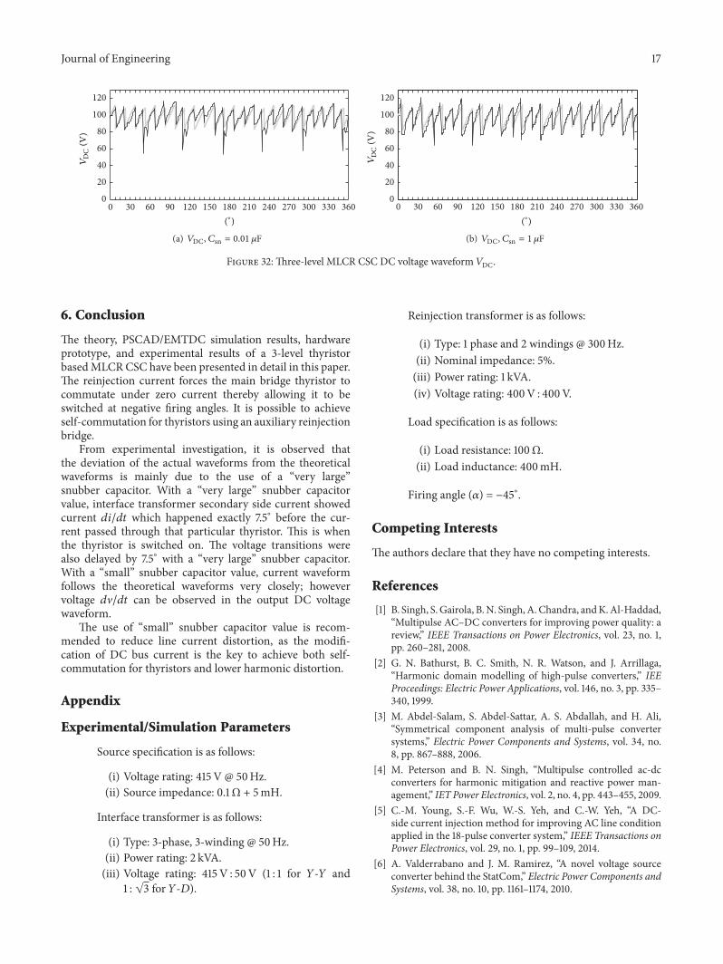
𝑚with 𝐶sn = 0.01 𝜇F is clearly reflected across
𝑉DC whereas the voltage 𝑑V/𝑑𝑡 transitions are not observed in𝑉DC with 𝐶sn = 1 𝜇F. Nevertheless, 𝑉DC has 24 pulses in boththe cases which implies that ripple voltage is getting added to𝑉𝑥giving it 24-pulse characteristics.

16 Journal of Engineering
15030 180 270240 3000 12060 330210 36090
I a(A
)
−0.5−0.4−0.3−0.2−0.1
00.10.20.30.40.5
(∘)
(a) 𝐼𝑎, 𝐶sn = 0.01 𝜇F
−0.5
0
0.5
33030090 210300 270180150120 36024060
I a(A
)
(∘)
(b) 𝐼𝑎, 𝐶sn = 1 𝜇F
Figure 28: Primary side line current 𝐼𝑎
.
360600 30 21090 270 300120 180 240150 3300
20
40
60
80
100
Vy,V
d(V
)
(∘)
(a) 𝑉𝑦and 𝑉𝑑, 𝐶sn = 0.01 𝜇F
Vy,V
d(V
)
360600 30 21090 270 300120 180 240150 330(∘)
0
20
40
60
80
100
(b) 𝑉𝑦and 𝑉𝑑, 𝐶sn = 1 𝜇F
Figure 29: DC voltage waveforms 𝑉𝑦
and 𝑉𝑑
.
0
50
100
150
0 24030 150 210 36060 270180120 300 33090(∘)
Vx
(V)
(a) 𝑉𝑥, 𝐶sn = 0.01 𝜇F
1500 270120 300210 24090 330180 36030 600
20406080
100120140160
Vx
(V)
(∘)
(b) 𝑉𝑥, 𝐶sn = 1 𝜇F
Figure 30: 12-pulse DC voltage waveform 𝑉𝑥
.
240 270 300120 1506030 180900 330 360210−80−60−40−20
020406080
Vm
(V)
(∘)
(a) 𝑉𝑚, 𝐶sn = 0.01 𝜇F
240 270 300120 1506030 180900 330 360210(∘)
Vm
(V)
−80−60−40−20
020406080
(b) 𝑉𝑚, 𝐶sn = 1 𝜇F
Figure 31: Reinjection transformer secondary side voltage 𝑉𝑚
.
Journal of Engineering 17
30 1200 60 300 33090 240180 210 360150 2700
20
40
60
80
100
120
(∘)
VD
C(V
)
(a) 𝑉DC, 𝐶sn = 0.01 𝜇F
0
20
40
60
80
100
120
30 1200 60 300 33090 240180 210 360150 270(∘)
VD
C(V
)
(b) 𝑉DC, 𝐶sn = 1 𝜇F
Figure 32: Three-level MLCR CSC DC voltage waveform 𝑉DC.
6. Conclusion
The theory, PSCAD/EMTDC simulation results, hardwareprototype, and experimental results of a 3-level thyristorbasedMLCRCSC have been presented in detail in this paper.The reinjection current forces the main bridge thyristor tocommutate under zero current thereby allowing it to beswitched at negative firing angles. It is possible to achieveself-commutation for thyristors using an auxiliary reinjectionbridge.
From experimental investigation, it is observed thatthe deviation of the actual waveforms from the theoreticalwaveforms is mainly due to the use of a “very large”snubber capacitor. With a “very large” snubber capacitorvalue, interface transformer secondary side current showedcurrent 𝑑𝑖/𝑑𝑡 which happened exactly 7.5∘ before the cur-rent passed through that particular thyristor. This is whenthe thyristor is switched on. The voltage transitions werealso delayed by 7.5∘ with a “very large” snubber capacitor.With a “small” snubber capacitor value, current waveformfollows the theoretical waveforms very closely; howevervoltage 𝑑V/𝑑𝑡 can be observed in the output DC voltagewaveform.
The use of “small” snubber capacitor value is recom-mended to reduce line current distortion, as the modifi-cation of DC bus current is the key to achieve both self-commutation for thyristors and lower harmonic distortion.
Appendix
Experimental/Simulation Parameters
Source specification is as follows:
(i) Voltage rating: 415V @ 50Hz.(ii) Source impedance: 0.1Ω + 5mH.
Interface transformer is as follows:
(i) Type: 3-phase, 3-winding @ 50Hz.(ii) Power rating: 2 kVA.(iii) Voltage rating: 415V : 50V (1 : 1 for 𝑌-𝑌 and
1 :√3 for 𝑌-𝐷).
Reinjection transformer is as follows:
(i) Type: 1 phase and 2 windings @ 300Hz.(ii) Nominal impedance: 5%.(iii) Power rating: 1 kVA.(iv) Voltage rating: 400V : 400V.
Load specification is as follows:
(i) Load resistance: 100Ω.(ii) Load inductance: 400mH.
Firing angle (𝛼) = −45∘.
Competing Interests
The authors declare that they have no competing interests.
References
[1] B. Singh, S. Gairola, B.N. Singh,A. Chandra, andK.Al-Haddad,“Multipulse AC–DC converters for improving power quality: areview,” IEEE Transactions on Power Electronics, vol. 23, no. 1,pp. 260–281, 2008.
[2] G. N. Bathurst, B. C. Smith, N. R. Watson, and J. Arrillaga,“Harmonic domain modelling of high-pulse converters,” IEEProceedings: Electric Power Applications, vol. 146, no. 3, pp. 335–340, 1999.
[3] M. Abdel-Salam, S. Abdel-Sattar, A. S. Abdallah, and H. Ali,“Symmetrical component analysis of multi-pulse convertersystems,” Electric Power Components and Systems, vol. 34, no.8, pp. 867–888, 2006.
[4] M. Peterson and B. N. Singh, “Multipulse controlled ac-dcconverters for harmonic mitigation and reactive power man-agement,” IET Power Electronics, vol. 2, no. 4, pp. 443–455, 2009.
[5] C.-M. Young, S.-F. Wu, W.-S. Yeh, and C.-W. Yeh, “A DC-side current injection method for improving AC line conditionapplied in the 18-pulse converter system,” IEEE Transactions onPower Electronics, vol. 29, no. 1, pp. 99–109, 2014.
[6] A. Valderrabano and J. M. Ramirez, “A novel voltage sourceconverter behind the StatCom,” Electric Power Components andSystems, vol. 38, no. 10, pp. 1161–1174, 2010.

18 Journal of Engineering
[7] C. I. Odeh, D. B. Nnadi, and E. S. Obe, “Three-phase, five-levelmulti-level inverter topology,” Electric Power Components andSystems, vol. 40, no. 13, pp. 1522–1532, 2012.
[8] C. I.Odeh andD. B.N.Nnadi, “Single-phase, 17-level hybridizedcascaded multi-level inverter,” Electric Power Components andSystems, vol. 41, no. 2, pp. 182–196, 2013.
[9] A. Lesnicar and R. Marquardt, “An innovative modular mul-tilevel converter topology suitable for a wide power range,” inProceedings of the IEEE Power Tech Conference (POWERTECH’03), vol. 3, pp. 1–6, Bologona, Italy, June 2003.
[10] J. I. Guzman, P. E. Melın, J. R. Espinoza et al., “Digitalimplementation of selective harmonic elimination techniquesin modular current source rectifiers,” IEEE Transactions onIndustrial Informatics, vol. 9, no. 2, pp. 1167–1177, 2013.
[11] J. Wu, Z.-X. Wang, G.-Q. Wang, S. Li, and D.-G. Wu, “Researchon direct power control of modular multi-level converter forpower transmission,” Electric Power Components and Systems,vol. 40, no. 15, pp. 1731–1749, 2012.
[12] S. Li, Z.Wang, andG.Wang, “Proportional-integral-differentialneural network based sliding-mode controller for modularmulti-level high-voltage DC converter of offshore wind power,”Electric Power Components and Systems, vol. 41, no. 4, pp. 427–446, 2013.
[13] S. M. Muyeen, R. Takahashi, and J. Tamura, “Operation andcontrol of HVDC-connected offshore wind farm,” IEEE Trans-actions on Sustainable Energy, vol. 1, no. 1, pp. 30–37, 2010.
[14] Y. H. Liu, Multi-level voltage and current reinjection AC-DCconversion [Ph.D. thesis], Electrical and Computer EngineeringDepartment, University of Canterbury, Christchurch, NewZealand, 2003.
[15] J. F. Baird and J. Arrilaga, “Harmonic reduction in DC-ripplereinjection,” IEE Proceedings C, vol. 127, no. 5, pp. 294–303, 1980.
[16] J. Arrillaga, L. Yonghe, C. S. Crimp, and M. Villablanca,“Harmonic elimination by DC ripple reinjection in generator-convertor units operating at variable speeds,” IEE ProceedingsC: Generation Transmission and Distribution, vol. 140, no. 1, pp.57–64, 1993.
[17] J. Arrilaga, Y. H. Liu, L. B. Perera, and N. R. Watson, “A cur-rent reinjection scheme that adds self-commutation and pulsemultiplication to the thyristor converter,” IEEE Transactions onPower Delivery, vol. 21, no. 3, pp. 1593–1599, 2006.
[18] L. B. Perera, N. R.Watson, Y. H. Liu, and J. Arrillaga, “Multilevelcurrent reinjection self-commutated HVDC converter,” IEEProceedings—Generation, Transmission and Distribution, vol.152, no. 5, pp. 607–615, 2005.
[19] W. McMurray, “Selection of snubbers and clamps to optimizethe design of transistor switching converters,” IEEE Transac-tions on Industry Applications, vol. IA-16, no. 4, pp. 513–523,1980.
[20] LEM,Voltage Transducer, LV25-P datasheet, no. 060315/4, 2012,http://www.lem.com.
[21] Murata Power Solutions, 772 Series Pulse transformers,datasheet, 2011, http://www.murata-ps.com/.
[22] NXP Semiconductors, BT152 SeriesThyristors, Datasheet, 1997,http://www.nxp.com.
[23] Avago Technologies, “Automotive IGBT gate drive optocouplerwith 𝑅2 coupler isolation and 2.5 Amp output current,” ACPL-312T Datasheet, 2011.
[24] IXYS Semiconductors, IGBT IXGP20N120, datasheet, 2002,http://www.avagotech.com/.
[25] XP Power, 2 Watts IL Series, IL0515S datasheet, 2012, http://www.xppower.com.

International Journal of
AerospaceEngineeringHindawi Publishing Corporationhttp://www.hindawi.com Volume 2014
RoboticsJournal of
Hindawi Publishing Corporationhttp://www.hindawi.com Volume 2014
Hindawi Publishing Corporationhttp://www.hindawi.com Volume 2014
Active and Passive Electronic Components
Control Scienceand Engineering
Journal of
Hindawi Publishing Corporationhttp://www.hindawi.com Volume 2014
International Journal of
RotatingMachinery
Hindawi Publishing Corporationhttp://www.hindawi.com Volume 2014
Hindawi Publishing Corporation http://www.hindawi.com
Journal ofEngineeringVolume 2014
Submit your manuscripts athttp://www.hindawi.com
VLSI Design
Hindawi Publishing Corporationhttp://www.hindawi.com Volume 2014
Hindawi Publishing Corporationhttp://www.hindawi.com Volume 2014
Shock and Vibration
Hindawi Publishing Corporationhttp://www.hindawi.com Volume 2014
Civil EngineeringAdvances in
Acoustics and VibrationAdvances in
Hindawi Publishing Corporationhttp://www.hindawi.com Volume 2014
Hindawi Publishing Corporationhttp://www.hindawi.com Volume 2014
Electrical and Computer Engineering
Journal of
Advances inOptoElectronics
Hindawi Publishing Corporation http://www.hindawi.com
Volume 2014
The Scientific World JournalHindawi Publishing Corporation http://www.hindawi.com Volume 2014
SensorsJournal of
Hindawi Publishing Corporationhttp://www.hindawi.com Volume 2014
Modelling & Simulation in EngineeringHindawi Publishing Corporation http://www.hindawi.com Volume 2014
Hindawi Publishing Corporationhttp://www.hindawi.com Volume 2014
Chemical EngineeringInternational Journal of Antennas and
Propagation
International Journal of
Hindawi Publishing Corporationhttp://www.hindawi.com Volume 2014
Hindawi Publishing Corporationhttp://www.hindawi.com Volume 2014
Navigation and Observation
International Journal of
Hindawi Publishing Corporationhttp://www.hindawi.com Volume 2014
DistributedSensor Networks
International Journal of