resolution d7 main - eth z · the multi-modulus divider (mmd) consists of several div-2/3 blocks....
TRANSCRIPT
RESOLUTION Project IST - 026851 Design of BS synthesiser on advanced CMOS technology [D7]
Document Information
Title D7 – Design of BS synthesiser on advanced CMOS technology
Workpackage WP4 – CMOS systems
Responsible FAU
Due Date Project Month 15 (April 2007)
Type Prototype
Status Version 1.0
Security Public
Authors Thomas Ußmüller
Project URL http://www.ife.ee.ethz.ch/RESOLUTION/
RESOLUTION Reconfigurable Systems for Mobile Local Communication and Positioning

D7 – Design of BS synthesiser on advanced CMOS
technology Page 2
RESOLUTION 2007-04-30
Table of contents 1 INTRODUCTION ............................................................................................. 3
2 SYNTHESISER SPECIFICATION ...................................................................... 3
3 SYNTHESISER ARCHITECTURE ....................................................................... 3
3.1 PHASE-FREQUENCY DETECTOR ............................................................................ 5
3.2 CHARGE-PUMP ................................................................................................ 5
3.3 LOOP FILTER .................................................................................................. 6
3.4 CML STANDARD CELL LIBRARY ........................................................................... 7
3.5 MMD ARCHITECTURE ....................................................................................... 7
3.6 VCO ARCHITECTURE ........................................................................................ 8
4 MEASUREMENT RESULTS ............................................................................... 9
4.1 MEASUREMENT RESULTS OF THE DIVIDER .............................................................. 9
4.2 MEASUREMENT RESULTS OF THE VCO ................................................................ 10
4.2.1 OUTPUT SPECTRUM ....................................................................................... 10
4.2.2 HARMONICS ............................................................................................... 11
4.2.3 TUNING-RANGE ........................................................................................... 12
4.2.4 VCO PUSHING ............................................................................................ 13
4.2.5 PHASE-NOISE ............................................................................................. 14
4.2.6 COMPARISON WITH OTHER PUBLISHED VCOS ........................................................ 15
5 PCB FOR DEMONSTRATOR SYSTEM .............................................................. 16
5.1 DESIGN....................................................................................................... 16
5.2 MEASUREMENT RESULTS ................................................................................. 17
5.2.1 MEASUREMENT RESULTS OF THE DIVIDER ............................................................. 17
5.2.2 MEASUREMENT RESULTS OF THE VCO ................................................................. 17
5.2.3 MEASUREMENT RESULTS OF THE PHASED-LOCKED LOOP ............................................. 22
6 CONCLUSIONS ............................................................................................. 24
7 REFERENCES ................................................................................................ 24
D7 – Design of BS synthesiser on advanced CMOS
technology Page 3
RESOLUTION 2007-04-30
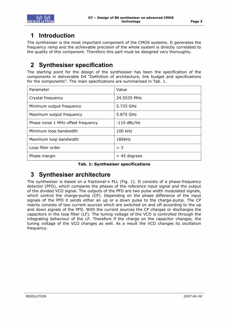
1 Introduction The synthesiser is the most important component of the CMOS systems. It generates the frequency ramp and the achievable precision of the whole system is directly correlated to the quality of this component. Therefore this part must be designed very thoroughly.
2 Synthesiser specification The starting point for the design of the synthesiser has been the specification of the components in deliverable D4 “Definition of architecture, link budget and specifications for the components”. The main specifications are summarised in Tab. 1.
Parameter Value
Crystal frequency 24.5535 MHz
Minimum output frequency 5.725 GHz
Maximum output frequency 5.875 GHz
Phase noise 1 MHz offset frequency -110 dBc/Hz
Minimum loop bandwidth 100 kHz
Maximum loop bandwidth 180kHz
Loop filter order > 3
Phase margin > 45 degrees
Tab. 1: Synthesiser specifications
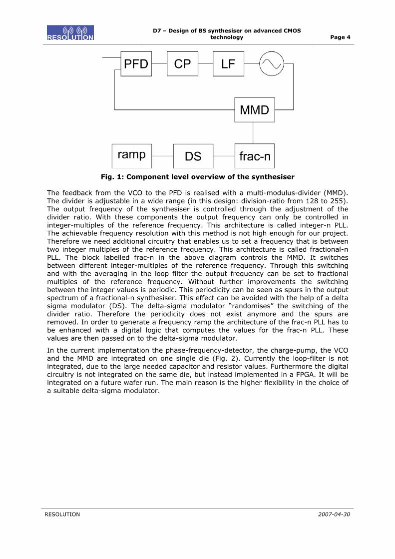
3 Synthesiser architecture The synthesiser is based on a fractional-n PLL (Fig. 1). It consists of a phase-frequency detector (PFD), which compares the phases of the reference input signal and the output of the divided VCO signal. The outputs of the PFD are two pulse width modulated signals, which control the charge-pump (CP). Depending on the phase difference of the input signals of the PFD it sends either an up or a down pulse to the charge-pump. The CP mainly consists of two current sources which are switched on and off according to the up and down signals of the PFD. With the current sources the CP charges or discharges the capacitors in the loop filter (LF). The tuning voltage of the VCO is controlled through the integrating behaviour of the LF. Therefore if the charge on the capacitor changes, the tuning voltage of the VCO changes as well. As a result the VCO changes its oscillation frequency.
D7 – Design of BS synthesiser on advanced CMOS
technology Page 4
RESOLUTION 2007-04-30
Fig. 1: Component level overview of the synthesiser
The feedback from the VCO to the PFD is realised with a multi-modulus-divider (MMD). The divider is adjustable in a wide range (in this design: division-ratio from 128 to 255). The output frequency of the synthesiser is controlled through the adjustment of the divider ratio. With these components the output frequency can only be controlled in integer-multiples of the reference frequency. This architecture is called integer-n PLL. The achievable frequency resolution with this method is not high enough for our project. Therefore we need additional circuitry that enables us to set a frequency that is between two integer multiples of the reference frequency. This architecture is called fractional-n PLL. The block labelled frac-n in the above diagram controls the MMD. It switches between different integer-multiples of the reference frequency. Through this switching and with the averaging in the loop filter the output frequency can be set to fractional multiples of the reference frequency. Without further improvements the switching between the integer values is periodic. This periodicity can be seen as spurs in the output spectrum of a fractional-n synthesiser. This effect can be avoided with the help of a delta sigma modulator (DS). The delta-sigma modulator “randomises” the switching of the divider ratio. Therefore the periodicity does not exist anymore and the spurs are removed. In order to generate a frequency ramp the architecture of the frac-n PLL has to be enhanced with a digital logic that computes the values for the frac-n PLL. These values are then passed on to the delta-sigma modulator.
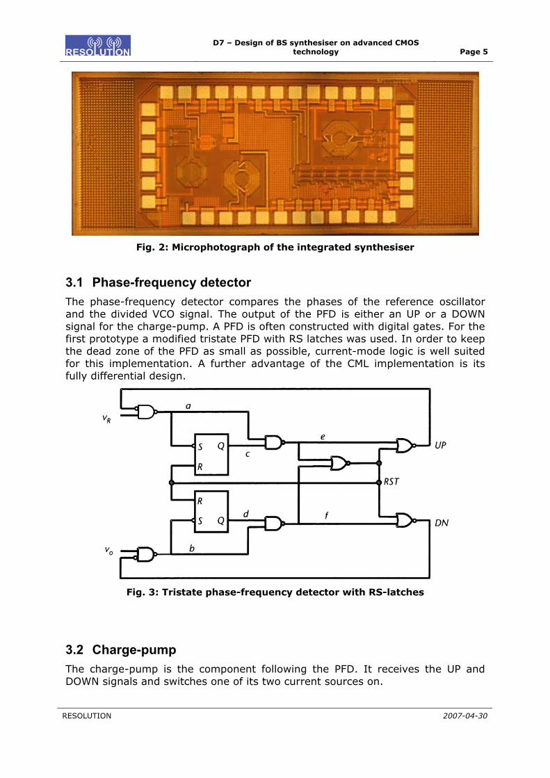
In the current implementation the phase-frequency-detector, the charge-pump, the VCO and the MMD are integrated on one single die (Fig. 2). Currently the loop-filter is not integrated, due to the large needed capacitor and resistor values. Furthermore the digital circuitry is not integrated on the same die, but instead implemented in a FPGA. It will be integrated on a future wafer run. The main reason is the higher flexibility in the choice of a suitable delta-sigma modulator.
D7 – Design of BS synthesiser on advanced CMOS
technology Page 5
RESOLUTION 2007-04-30
Fig. 2: Microphotograph of the integrated synthesiser
3.1 Phase-frequency detector The phase-frequency detector compares the phases of the reference oscillator and the divided VCO signal. The output of the PFD is either an UP or a DOWN signal for the charge-pump. A PFD is often constructed with digital gates. For the first prototype a modified tristate PFD with RS latches was used. In order to keep the dead zone of the PFD as small as possible, current-mode logic is well suited for this implementation. A further advantage of the CML implementation is its fully differential design.
Fig. 3: Tristate phase-frequency detector with RS-latches
3.2 Charge-pump The charge-pump is the component following the PFD. It receives the UP and DOWN signals and switches one of its two current sources on.
D7 – Design of BS synthesiser on advanced CMOS
technology Page 6
RESOLUTION 2007-04-30
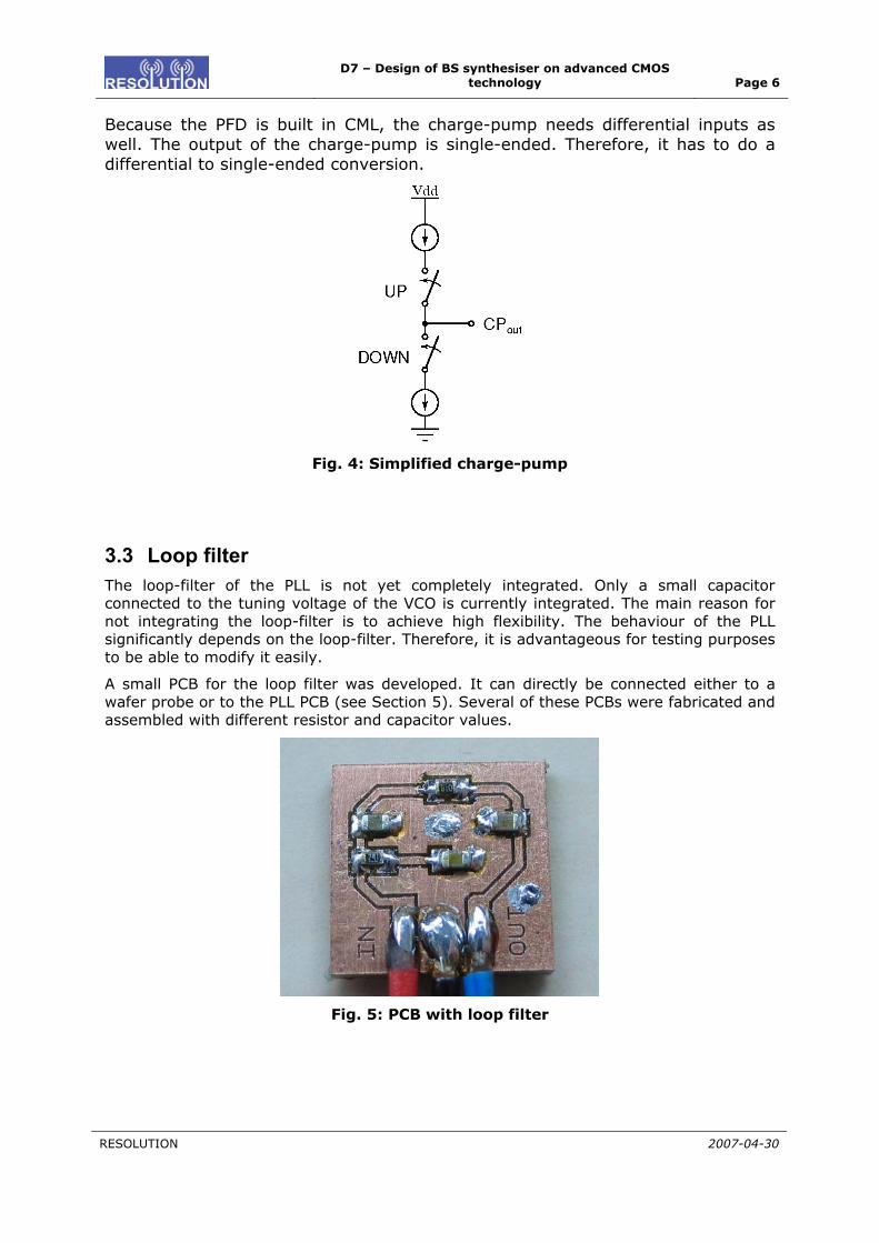
Because the PFD is built in CML, the charge-pump needs differential inputs as well. The output of the charge-pump is single-ended. Therefore, it has to do a differential to single-ended conversion.
Fig. 4: Simplified charge-pump
3.3 Loop filter The loop-filter of the PLL is not yet completely integrated. Only a small capacitor connected to the tuning voltage of the VCO is currently integrated. The main reason for not integrating the loop-filter is to achieve high flexibility. The behaviour of the PLL significantly depends on the loop-filter. Therefore, it is advantageous for testing purposes to be able to modify it easily.
A small PCB for the loop filter was developed. It can directly be connected either to a wafer probe or to the PLL PCB (see Section 5). Several of these PCBs were fabricated and assembled with different resistor and capacitor values.
Fig. 5: PCB with loop filter
D7 – Design of BS synthesiser on advanced CMOS
technology Page 7
RESOLUTION 2007-04-30
3.4 CML standard cell library Several components used in a PLL can be realised with digital logic. These include the phase-frequency-detector and especially the multi-modulus divider. Using standard CMOS logic causes several difficulties:
• the CMOS logic needs a different supply voltage
• CMOS is very noisy and can disturb the analogue components
• CMOS is not fast enough for the divider
Because of these reasons á standard cell library in current-mode logic (CML) was designed. CML gates consist mainly of a current source and several differential pairs. If the amplitude of the input signal is large enough the differential pairs work as switches. They switch the current of the source to one path. This causes a voltage drop at the resistor and, therefore, a low logic level is achieved at this output. Because no current flows in the other path the second output has a logic high level. As an example of this library, in Fig. 6 an AND-gate in this logic is shown.
Fig. 6: AND-gate in current-mode logic
3.5 MMD architecture The Multi-modulus divider (MMD) consists of several DIV-2/3 blocks. Each of these blocks can either divide the input signal by two or by three. The used divider has seven cascaded DIV-2/3 stages so that a division ration between 128 and 255 can be set. All inputs controlling the division ratio of the MMD are connected to pads and can be controlled by external circuitry, e.g. an FPGA. With this implementation the PLL can work in integer-n as well as fractional-n mode.

D7 – Design of BS synthesiser on advanced CMOS
technology Page 8
RESOLUTION 2007-04-30
Fig. 7: Divide stage (2/3) of multi-modulus divider
3.6 VCO architecture For integrated circuit design three different VCO topologies are commonly used:
• Multivibrators
• Ring oscillators
• LC oscillators
Due to the stringent requirements for phase-noise of the VCO in communication and positioning systems, mainly LC oscillator topologies were investigated. The most common used LC oscillator topologies are the Collpits- and the cross-coupled-oscillator. A drawback of the Collpits VCO compared to the cross-coupled VCO is the lower loop gain. This can be compensated with a higher tail current, but this increases the power consumption, which is not desired in mobile applications. The cross-coupled oscillator on the other hand has a higher loop gain and therefore has lower power consumption, but the phase noise performance is worse. To overcome the drawbacks of both architectures a new topology published by Xiaoyong Li et al [1][2] has been used. This topology is based on a Collpits-VCO in common-gate configuration. The gates of the transistors are not connected to a constant biasing voltage like in the case of a conventional Collpits-oscillator. Instead at the gate a voltage that has a phase shift of 180° the voltage at the LC-tank is applied. If the transistor is switched off, the non-constant biasing voltage has no effect on the circuit operation. But when the transistor is switched on to compensate the losses in the LC-tank the gate-source voltage is twice as high as it would be with constant biasing. Therefore the effective transconductance is increased. The required effective transconductance is given by the quality factor of the LC-tank. Thus for the same LC-tank the tail current of the gm-boosted VCO can be reduced compared to the classical Collpits-oscillator.

D7 – Design of BS synthesiser on advanced CMOS
technology Page 9
RESOLUTION 2007-04-30
Fig. 8: Architecture of the VCO
In analogue radio frequency integrated circuits the VCO is usually built with a differential architecture to reduce the effect of substrate noise coupling. This is a great advantage for the gm-boosted VCO. A voltage with the necessary phase-shift and amplitude that is sufficiently large is available at the other path of the VCO. The gate can either be connected to the source or the drain of the other transistor. It is advantageous to connect it the drain as no further biasing is necessary then.
4 Measurement results
4.1 Measurement results of the divider For the test of the divider the VCO is running at a fixed frequency. The division ration is set through external pads and the output signal of the divider is observed with an oscilloscope at the MMDout pad of the PLL.
1
1.1
1.2
1.3
1.4
1.5
1.6
1.7
1.8
1.9
2
2.1
-20 0 20 40 60 80 100
ampl
itude
(in
V)
time (in ns)
0
0.1
0.2
0.3
0.4
0.5
0.6
0.7
0.8
0.9
-10 0 10 20 30 40 50
ampl
itude
(in
V)
time (in ns)
Fig. 9: Output signal of the MMD

D7 – Design of BS synthesiser on advanced CMOS
technology Page 10
RESOLUTION 2007-04-30
In Fig. 9, the measurement results show the minimum and maximum value of the division ratio of the divider. It can be seen that the switching of the division ratios works well. However, the output waveform of the divider can be improved. Nonetheless, the problematic component is not the output buffer but the circuit translating the differential current-mode logic signals to CMOS signals. With an improved topology for the converter this problem can be fixed easily in the redesign phase.
4.2 Measurement results of the VCO Lots of the parameters of a PLL depend on the voltage controlled oscillator (VCO). It is the most important component of the PLL. Therefore it is wise to first measure it independently of the other building blocks of the PLL.
The output of the VCO is differential. Therefore the device under test (DUT) is connected to a rat-race coupler, which is used as balun. The two balanced ports are connected to the DUT and the unbalanced port is directly connected to a signal source analyser. The supply and biasing voltages are as well connected to the signal source analyser.
4.2.1 Output spectrum
The output spectrum of the VCO (Fig. 10) measured with a 3 MHz span shows the classical behaviour of an oscillator spectrum. Close to the carrier the spectrum has a 1/f3 characteristic. Above a corner frequency of about 300 kHz it shows a 1/f2 characteristic.
The spectrum is measured at a centre frequency of 6.37GHz with a resolution bandwidth of 3 kHz. Including the losses in the balun and the cables the measured differential output power of the VCO is -14dBm.
Depending on the capacitive load at the output of the multi-modulus divider, the spectrum shows spurs due to coupling through the substrate and through the supply voltage, which are not shown here.
D7 – Design of BS synthesiser on advanced CMOS
technology Page 11
RESOLUTION 2007-04-30
*
A
Att 30 dB
1 APCLRWR
Ref -10 dBm
SGL
300 kHz/Center 6.366185897 GHz Span 3 MHz
* RBW 3 kHz
VBW 10 kHz
SWT 340 ms
-130
-120
-110
-100
-90
-80
-70
-60
-50
-40
-30
-20
-101
Marker 1 [T1 ]
-14.45 dBm
6.366185897 GHz
Date: 23.MAR.2007 09:29:59
Fig. 10: Spectrum of the free running oscillator (span: 3 MHz)
4.2.2 Harmonics
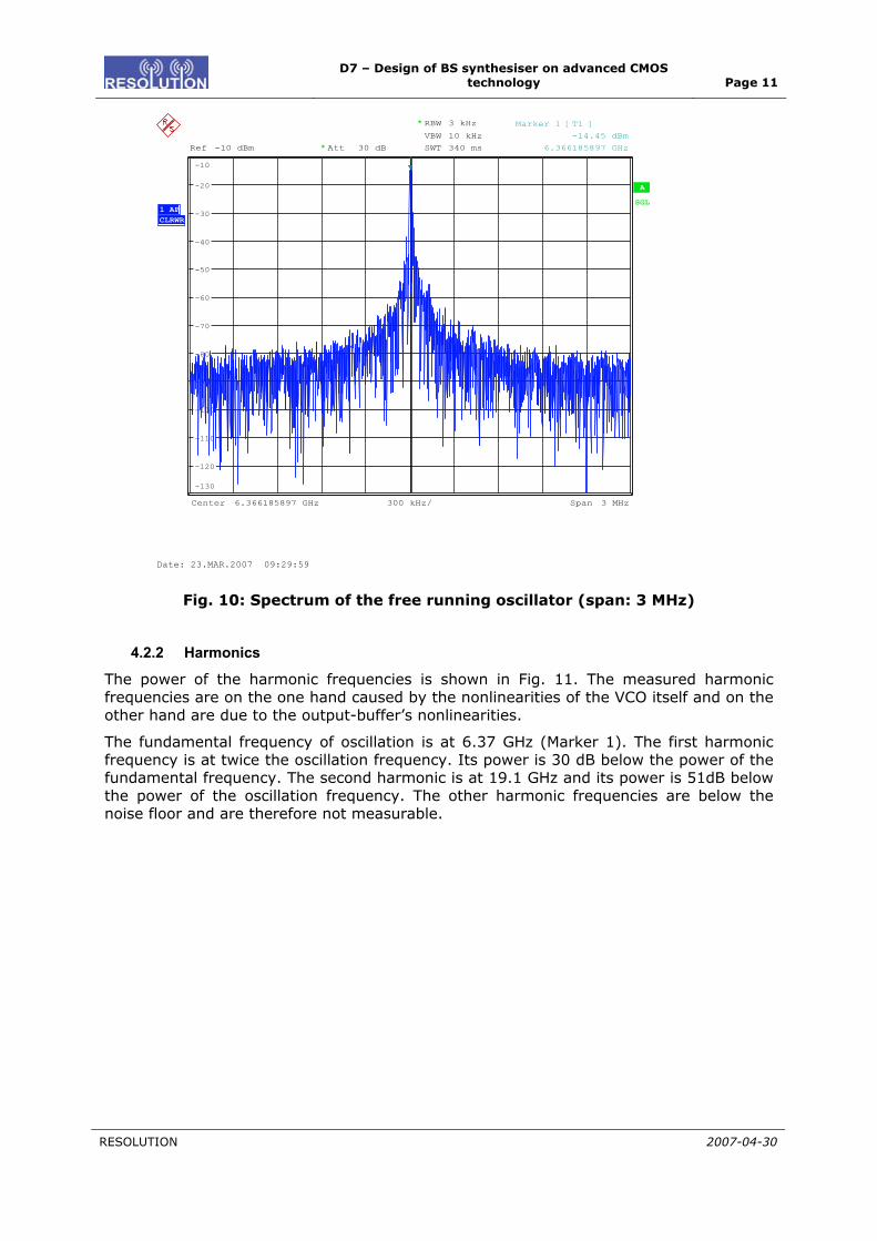
The power of the harmonic frequencies is shown in Fig. 11. The measured harmonic frequencies are on the one hand caused by the nonlinearities of the VCO itself and on the other hand are due to the output-buffer’s nonlinearities.
The fundamental frequency of oscillation is at 6.37 GHz (Marker 1). The first harmonic frequency is at twice the oscillation frequency. Its power is 30 dB below the power of the fundamental frequency. The second harmonic is at 19.1 GHz and its power is 51dB below the power of the oscillation frequency. The other harmonic frequencies are below the noise floor and are therefore not measurable.

D7 – Design of BS synthesiser on advanced CMOS
technology Page 12
RESOLUTION 2007-04-30
*
A
Att 30 dB
CLRWR
Ref -10 dBm
Center 13.25 GHz Span 26.5 GHz2.65 GHz/
SGL1 AP
* RBW 3 kHz
VBW 10 kHz
SWT 3000 s
-130
-120
-110
-100
-90
-80
-70
-60
-50
-40
-30
-20
-10 1 Marker 1 [T1 ]
-15.69 dBm
6.370192308 GHz
2
Marker 2 [T1 ]
-45.42 dBm
12.740384615 GHz
3
Marker 3 [T1 ]
-66.62 dBm
19.110576923 GHz
Date: 23.MAR.2007 10:41:04
Fig. 11: Power of harmonic frequencies
4.2.3 Tuning-range
The tuning range describes the output frequency range that the oscillator is able to generate. The blue curve in Fig. 12 shows this characteristic for the measured VCO. The lower end of the tuning range (5.9 GHz) is at Vtune = 0V. The maximum measured frequency of 6.4 GHz is reached at Vtune = VDD. Unfortunately due to the high process variations the oscillation frequency of the VCO is slightly above the specification. These variations cause a frequency shift of only 6% with respect to the centre frequency. However, the tuning-range can be effortlessly improved in an upcoming redesign. Here, the coil or the varactors will be adjusted to meet the frequency specifications of the tuning range.
The whole tuning range is about 0.5 GHz or 8% of the centre frequency of the VCO. When connected to the PLL the tuning voltage is typically between 0.3 and 2.2 V due to the saturation voltage of the output transistors of the charge-pump.
The derivative of the tuning range is the tuning sensitivity KVCO. It is defined as the frequency change per voltage change (green curve, Fig. 12). Ideally the tuning sensitivity would be constant but in practice especially when the output frequency is close to the minimal or maximal possible frequency this is not the case.

D7 – Design of BS synthesiser on advanced CMOS
technology Page 13
RESOLUTION 2007-04-30
Measurement Aborted
R&S FSUP Signal Source Analyzer
Settings Results
Tuning Voltage Frequency Sensitivity Level
Vmin 0.00 V 5.896 GHz 4.73 MHz/V -17.50 dBm
Vcurrent 454.55 mV 5.905 GHz 36.12 MHz/V -17.51 dBm
Vmax 2.50 V 6.369 GHz 22.30 MHz/V -13.58 dBm
Tuning Characteristics
Frequency Sensitivity Top 7.1 GHz 750 MHz/V
-150.00
-50.00
50.00
150.00
250.00
350.00
450.00
550.00
650.00
0.0 V 2.5 V250.0 mV/div
5.30
5.50
5.70
5.90
6.10
6.30
6.50
6.70
6.90
1 FREQ
2 SENS
* A
Tuning Voltage
Date: 23.MAR.2007 10:49:21
Fig. 12: Tuning range and tuning sensitivity of the VCO
4.2.4 VCO pushing
Frequency pushing is the variation of the VCO output frequency due to a change in the power supply voltage VDD. The blue graph in Fig. 13 shows the behaviour at the nominal supply voltage. The black and green diagrams show the tuning range for a 10% increased and 10% decreased supply voltage respectively.
The sensitivity of the measured VCO to supply voltage variations arises from the fact that the biasing voltage of the varactors is direct proportional to VDD. This is necessary to achieve the maximum possible tuning range. Therefore a trade-off between tuning-range, phase-noise and pushing characteristic must be found.

D7 – Design of BS synthesiser on advanced CMOS
technology Page 14
RESOLUTION 2007-04-30
Running ...
R&S FSUP Signal Source Analyzer
Settings Results
Tuning Voltage Frequency @ Udc ?F @ Udc -250 mV ?F @ Udc +250 mV
Vmin 0.00 V 5.896 GHz -9.210 MHz 6.779 MHz
Vcurrent 1.62 V 6.253 GHz 1.490 MHz -14.221 MHz
Vmax 2.50 V 6.369 GHz 1.500 MHz -14.201 MHz
Tuning Characteristics
Frequency Top 7.1 GHz
0.0 V 2.5 V250.0 mV/div
5.30
5.50
5.70
5.90
6.10
6.30
6.50
6.70
6.90
1 FREQ
2-250 mV
3+250 mV
A
Tuning Voltage
Date: 23.MAR.2007 11:00:48
Fig. 13: VCO pushing
4.2.5 Phase-noise
Phase noise is the most important metric for an oscillator. It is a random variation in the phase of the output signal of the oscillator. Usually the phase noise close to the carrier is dominated by the upconverted flicker noise of the oscillator components. In this region the phase noise is proportional to 1/f3. Above the cut-off frequency the phase noise is mainly composed of the thermal noise of the oscillator devices. The noise is proportional to 1/f2 in this region. Phase noise is defined as the ratio of the output power at the oscillation frequency divided by the noise power in a 1Hz bandwidth.
The phase noise differs with the oscillation frequency. One reason for this effect is the varying quality factor of the varactor. The other reason is the difference in KVCO, as a higher KVCO makes the oscillator more sensitive to upconversion effects and noise at the tuning input.
The measurement in Fig. 14 shows a phase noise performance of -117dBc/Hz at the upper limit of the tuning range, which is a very good result for an oscillator consuming less than 5mW of power. At frequencies with higher KVCO the phase noise performance decreases.

D7 – Design of BS synthesiser on advanced CMOS
technology Page 15
RESOLUTION 2007-04-30
Running ...
R&S FSUP Signal Source Analyzer LOC KED
Settings Residual Noise Phase Detector +0 dB
Signal Frequency: 6.366086 GHz Evaluation from 1 kHz to 10 MHz
Signal Level: -13.2 dBm Residual PM 186.728 °
PLL Mode Harmonic 1 Residual FM 9.646 kHz
Internal Ref Tuned Internal Phase Det RMS Jitter 81.4768 ps
Phase Noise [dBc/Hz] Marker 1 [T1]
RF Atten 0 dB 1 MHz Top -20 dBc/Hz -116.56 dBc/Hz
10 kHz 100 kHz 1 MHz1 kHz 10 MHz
-120
-100
-80
-60
-40
LoopBW
1 CLRWRSMTH 1%
2 CLRWR
A
PA
1
Date: 23.MAR.2007 11:10:50
Fig. 14: Measured phase-noise of the VCO
4.2.6 Comparison with other published VCOs
The phase noise as well as the tuning range is a critical parameter of a VCO. They are closely correlated to each other. The higher the tuning range the higher the value of the varactor. But because the varactors usually have a poor quality factor, this decreases the quality factor of the LC-tank itself and the phase noise performance decreases. Therefore, it is not reasonable to compare VCOs which have different tuning ranges with the classical FOM:
dBmDCC
PfffLFOM ,log20)( +⎟⎟⎠
⎞⎜⎜⎝
⎛ Δ+Δ=
Therefore a new figure of merit proposed by Jonghae Kim et al [3] is used:
dBmDCC
FTR PFTRfffLFOM ,%10
log20)( +⎟⎟⎠
⎞⎜⎜⎝
⎛⋅
Δ+Δ=
L(Δf) describes the phase-noise at an offset frequency Δf. The second term takes the oscillation frequency into account, as the phase noise increases with increasing frequency. Furthermore the term FTR/10% has been added to the classical FOM for VCOs. This term takes the tuning range into account. The last term of the formula describes the power consumption, as the phase-noise decreases with increasing power. A comparison between this work and other published VCOs is shown in Tab. 2.

D7 – Design of BS synthesiser on advanced CMOS
technology Page 16
RESOLUTION 2007-04-30
Ref. FTR (%) Phase Noise (dBc/Hz)
Power (mW) FOMFTR
[4] 6% -90.5 13 -148.9
[5] 7% -101 5 -164.8
[6] 4% -110 11 -165.6
[7] 18% -114 14 -181.6
[3] 22% -101 10 -171.8
[3] 24% -110 10 -181.6
This work 8% -117 5 -187.6
Tab. 2: Comparison with other published VCOs in the 5 GHz frequency range
The phase-noise performance of the VCO is very good compared to other published VCOs. Especially remarkable is that the low phase-noise is achieved with extremely low power consumption at the same time.
5 PCB for demonstrator system
5.1 Design For a first demonstrator system a printed circuit board (PCB) was developed. The die is directly bonded on this PCB. The reference oscillator for the PLL can be connected through a SMA plug to the PCB. Furthermore connectors for attaching a FPGA board to the divider inputs/ outputs are available. The layout of the board is shown in Fig. 15.
Fig. 15: PCB for demonstrator system
D7 – Design of BS synthesiser on advanced CMOS
technology Page 17
RESOLUTION 2007-04-30
5.2 Measurement results
5.2.1 Measurement results of the divider
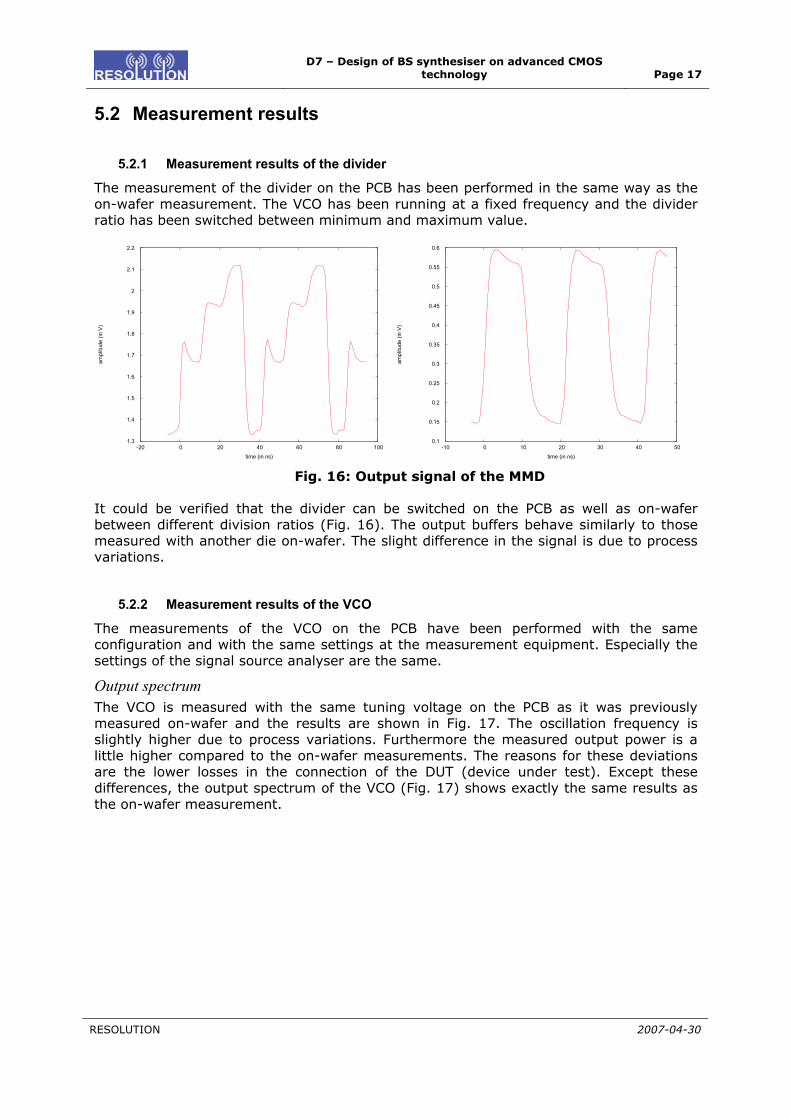
The measurement of the divider on the PCB has been performed in the same way as the on-wafer measurement. The VCO has been running at a fixed frequency and the divider ratio has been switched between minimum and maximum value.
1.3
1.4
1.5
1.6
1.7
1.8
1.9
2
2.1
2.2
-20 0 20 40 60 80 100
ampl
itude
(in
V)
time (in ns)
0.1
0.15
0.2
0.25
0.3
0.35
0.4
0.45
0.5
0.55
0.6
-10 0 10 20 30 40 50
ampl
itude
(in
V)
time (in ns)
Fig. 16: Output signal of the MMD
It could be verified that the divider can be switched on the PCB as well as on-wafer between different division ratios (Fig. 16). The output buffers behave similarly to those measured with another die on-wafer. The slight difference in the signal is due to process variations.
5.2.2 Measurement results of the VCO
The measurements of the VCO on the PCB have been performed with the same configuration and with the same settings at the measurement equipment. Especially the settings of the signal source analyser are the same.
Output spectrum The VCO is measured with the same tuning voltage on the PCB as it was previously measured on-wafer and the results are shown in Fig. 17. The oscillation frequency is slightly higher due to process variations. Furthermore the measured output power is a little higher compared to the on-wafer measurements. The reasons for these deviations are the lower losses in the connection of the DUT (device under test). Except these differences, the output spectrum of the VCO (Fig. 17) shows exactly the same results as the on-wafer measurement.
D7 – Design of BS synthesiser on advanced CMOS
technology Page 18
RESOLUTION 2007-04-30
*
1 APCLRWR
A
Att 30 dBRef -10 dBm
300 kHz/Center 6.420182692 GHz Span 3 MHz
* RBW 3 kHz
VBW 10 kHz
SWT 340 ms
SGL
-110
-100
-90
-80
-70
-60
-50
-40
-30
-20
-101
Marker 1 [T1 ]
-12.53 dBm
6.420206731 GHz
Date: 11.MAY.2007 08:14:06
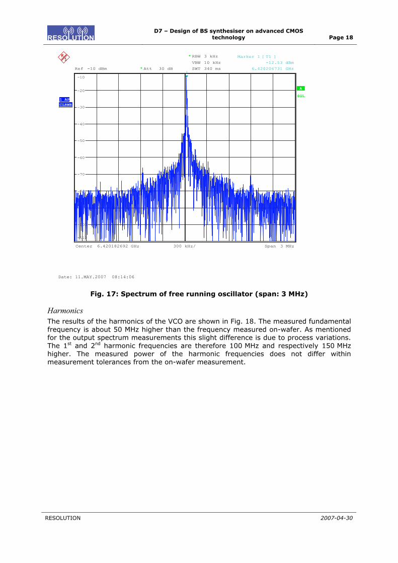
Fig. 17: Spectrum of free running oscillator (span: 3 MHz)
Harmonics The results of the harmonics of the VCO are shown in Fig. 18. The measured fundamental frequency is about 50 MHz higher than the frequency measured on-wafer. As mentioned for the output spectrum measurements this slight difference is due to process variations. The 1st and 2nd harmonic frequencies are therefore 100 MHz and respectively 150 MHz higher. The measured power of the harmonic frequencies does not differ within measurement tolerances from the on-wafer measurement.

D7 – Design of BS synthesiser on advanced CMOS
technology Page 19
RESOLUTION 2007-04-30
Ref -10 dBm Att 30 dB
RBW 3 kHz
VBW 10 kHz
SWT 3000 s*
*
Center 13.25 GHz Span 26.5 GHz2.65 GHz/
1 APCLRWR
* A
SGL
-110
-100
-90
-80
-70
-60
-50
-40
-30
-20
-10 1
Marker 1 [T1 ]
-15.06 dBm
6.412660256 GHz
2
Marker 2 [T1 ]
-48.40 dBm
12.825320513 GHz
3
Marker 3 [T1 ]
-64.40 dBm
19.280448718 GHz
Date: 11.MAY.2007 10:04:37
Fig. 18: Power of harmonic frequencies
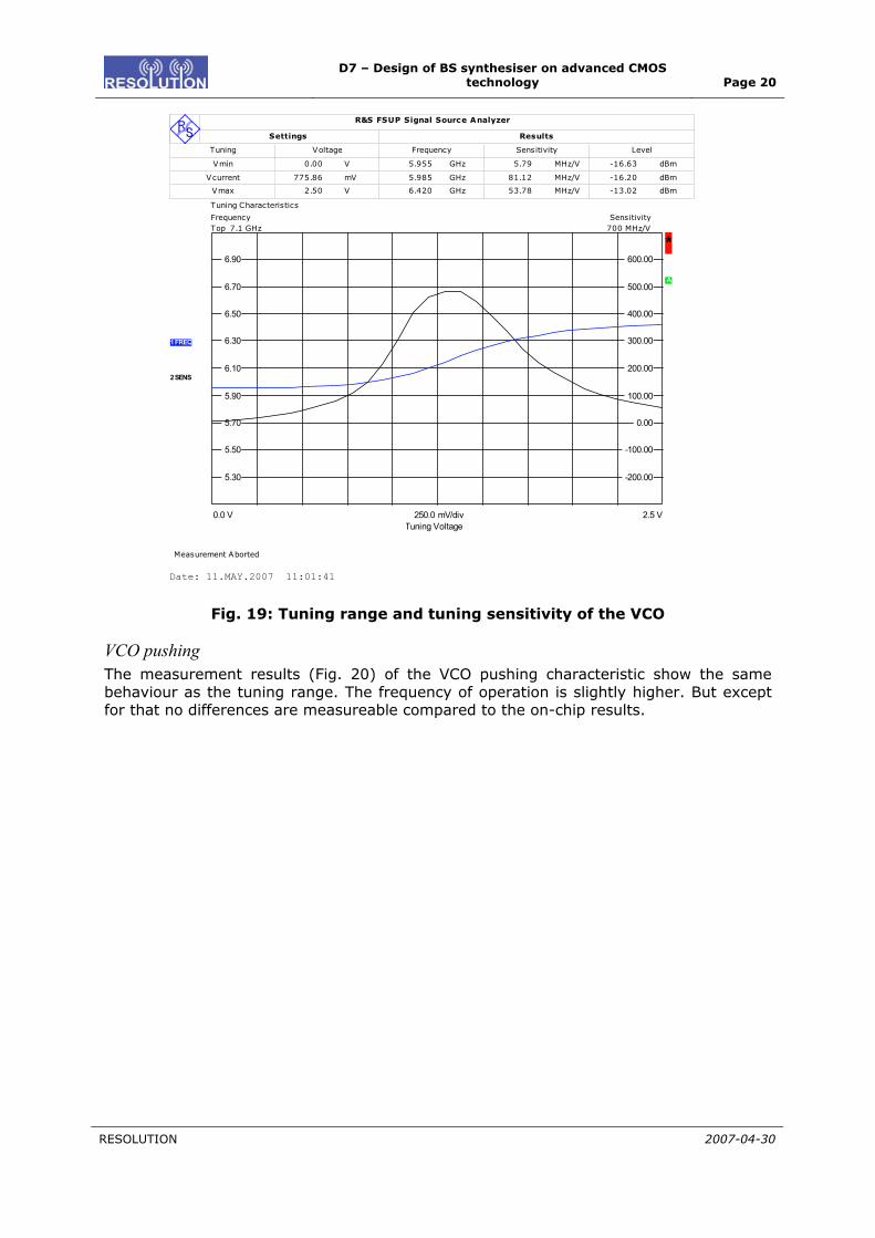
Tuning-range The measurement results of the tuning range and the tuning sensitivity are shown in Fig. 19. Except for the afore mentioned increase in the oscillation frequency compared to the on-wafer measurement, no difference in the tuning characteristic and tuning sensitivity is visible. The lower end of the tuning range is at 5.96 GHz. The upper end is 6.42 GHz. This tuning range does not meet exactly the specifications as indicated earlier. Nonetheless, the tuning-range can be effortlessly improved in the upcoming redesign by modifying the coil or the varactors.
D7 – Design of BS synthesiser on advanced CMOS
technology Page 20
RESOLUTION 2007-04-30
Measurement Aborted
R&S FSUP Signal Source Analyzer
Settings Results
Tuning Voltage Frequency Sensitivity Level
Vmin 0.00 V 5.955 GHz 5.79 MHz/V -16.63 dBm
Vcurrent 775.86 mV 5.985 GHz 81.12 MHz/V -16.20 dBm
Vmax 2.50 V 6.420 GHz 53.78 MHz/V -13.02 dBm
Tuning Characteristics
Frequency Sensitivity Top 7.1 GHz 700 MHz/V
-200.00
-100.00
0.00
100.00
200.00
300.00
400.00
500.00
600.00
0.0 V 2.5 V250.0 mV/div
5.30
5.50
5.70
5.90
6.10
6.30
6.50
6.70
6.90
1 FREQ
2 SENS
* A
Tuning Voltage
Date: 11.MAY.2007 11:01:41
Fig. 19: Tuning range and tuning sensitivity of the VCO
VCO pushing The measurement results (Fig. 20) of the VCO pushing characteristic show the same behaviour as the tuning range. The frequency of operation is slightly higher. But except for that no differences are measureable compared to the on-chip results.

D7 – Design of BS synthesiser on advanced CMOS
technology Page 21
RESOLUTION 2007-04-30
Measurement Aborted
R&S FSUP Signal Source Analyzer
Settings Results
Tuning Voltage Frequency @ Udc ?F @ Udc -250 mV ?F @ Udc +250 mV
Vmin 0.00 V 5.955 GHz -9.330 MHz 6.370 MHz
Vcurrent 2.16 V 6.394 GHz 26.364 MHz -13.510 MHz
Vmax 2.50 V 6.420 GHz 13.336 MHz -16.319 MHz
Tuning Characteristics
Frequency Top 7.1 GHz
0.0 V 2.5 V250.0 mV/div
5.30
5.50
5.70
5.90
6.10
6.30
6.50
6.70
6.90
1 FREQ
2-250 mV
3+250 mV
* A
Tuning Voltage
Date: 11.MAY.2007 11:03:20
Fig. 20: VCO pushing
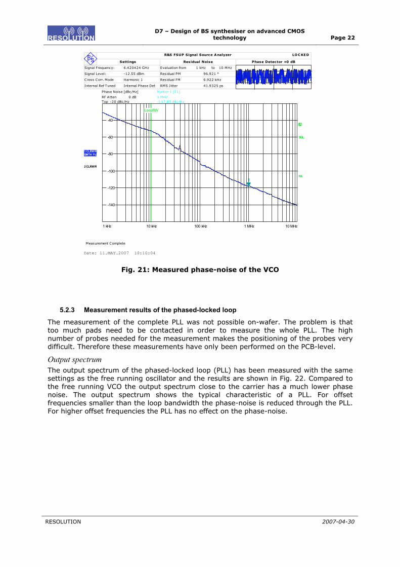
Phase-noise The phase-noise measurement on the PCB has been made at the same tuning voltage as the measurement on-wafer. As can be seen in Fig. 21 the operating frequency is slightly higher. The phase-noise performance has not changed within the tolerances of the measurement equipment at all.
D7 – Design of BS synthesiser on advanced CMOS
technology Page 22
RESOLUTION 2007-04-30
Measurement Complete
R&S FSUP Signal Source Analyzer LOC KED
Settings Residual Noise Phase Detector +0 dB
Signal Frequency: 6.420424 GHz Evaluation from 1 kHz to 10 MHz
Signal Level: -12.55 dBm Residual PM 96.921 °
Cross Corr. Mode Harmonic 1 Residual FM 6.922 kHz
Internal Ref Tuned Internal Phase Det RMS Jitter 41.9325 ps
Phase Noise [dBc/Hz] Marker 1 [T1]
RF Atten 0 dB 1 MHz Top -20 dBc/Hz -117.95 dBc/Hz
10 kHz 100 kHz 1 MHz1 kHz 10 MHz
-140
-120
-100
-80
-60
-40
LoopBW
1 CLRWRSMTH 1%
2 CLRWR
A
SGL
PA1
Date: 11.MAY.2007 10:10:04
Fig. 21: Measured phase-noise of the VCO
5.2.3 Measurement results of the phased-locked loop
The measurement of the complete PLL was not possible on-wafer. The problem is that too much pads need to be contacted in order to measure the whole PLL. The high number of probes needed for the measurement makes the positioning of the probes very difficult. Therefore these measurements have only been performed on the PCB-level.
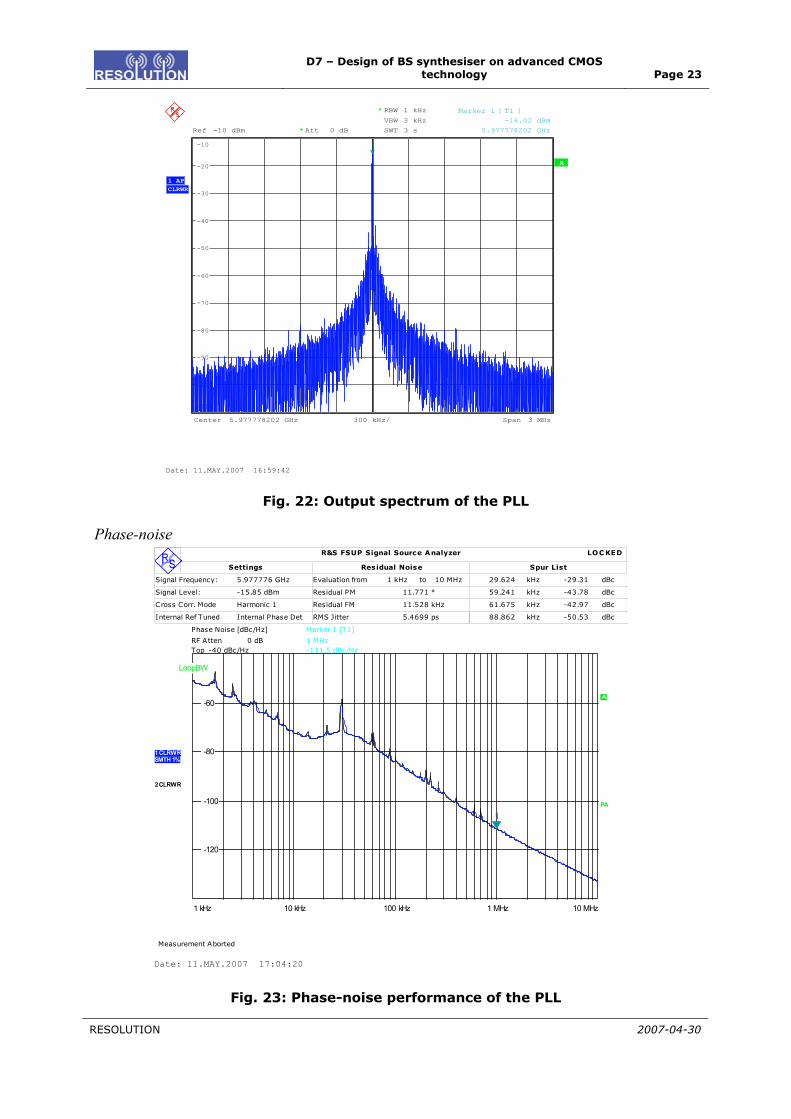
Output spectrum The output spectrum of the phased-locked loop (PLL) has been measured with the same settings as the free running oscillator and the results are shown in Fig. 22. Compared to the free running VCO the output spectrum close to the carrier has a much lower phase noise. The output spectrum shows the typical characteristic of a PLL. For offset frequencies smaller than the loop bandwidth the phase-noise is reduced through the PLL. For higher offset frequencies the PLL has no effect on the phase-noise.
D7 – Design of BS synthesiser on advanced CMOS
technology Page 23
RESOLUTION 2007-04-30
*
A
Att 0 dB
1 APCLRWR
Ref -10 dBm
300 kHz/Center 5.977778202 GHz Span 3 MHz
* RBW 1 kHz
VBW 3 kHz
SWT 3 s
-110
-100
-90
-80
-70
-60
-50
-40
-30
-20
-10 1
Marker 1 [T1 ]
-16.02 dBm
5.977778202 GHz
Date: 11.MAY.2007 16:59:42
Fig. 22: Output spectrum of the PLL
Phase-noise
Measurement Aborted
R&S FSUP Signal Source Analyzer LOC KED
Settings Residual Noise Spur List
Signal Frequency: 5.977776 GHz Evaluation from 1 kHz to 10 MHz
Signal Level: -15.85 dBm Residual PM 11.771 °
Cross Corr. Mode Harmonic 1 Residual FM 11.528 kHz
Internal Ref Tuned Internal Phase Det RMS Jitter 5.4699 ps
29.624 kHz -29.31 dBc
59.241 kHz -43.78 dBc
61.675 kHz -42.97 dBc
88.862 kHz -50.53 dBc
Phase Noise [dBc/Hz] Marker 1 [T1]
RF Atten 0 dB 1 MHz Top -40 dBc/Hz -111.5 dBc/Hz
10 kHz 100 kHz 1 MHz1 kHz 10 MHz
-120
-100
-80
-60
LoopBW
1 CLRWRSMTH 1%
2 CLRWR
A
PA
1
Date: 11.MAY.2007 17:04:20
Fig. 23: Phase-noise performance of the PLL
D7 – Design of BS synthesiser on advanced CMOS
technology Page 24
RESOLUTION 2007-04-30
The PLL has been measured with a second order loop filter with a cut-off frequency of about 100 kHz. The phase-noise of the complete PLL shows the afore mentioned characteristic (Fig. 23). It is reduced for frequencies close to the carrier. For higher offset frequencies no difference between the free running VCO and the PLL is measurable as can be seen at the phase-noise marker in a 1 MHz offset.
6 Conclusions A first prototype for the synthesiser in advanced CMOS technology was realised. The developed architecture is based on a fractional-n phased-locked loop to achieve a high frequency resolution. With an external reference oscillator with a fixed frequency, the ramp is generated through switching of the divider ratio of the MMD in the feedback path. All analogue components, the phase-frequency detector, the charge-pump, the multi-modulus-divider and the VCO, were integrated on a single integrated circuit. The loop filter was designed to operate externally in order to have a high flexibility during testing the synthesizer.
These manufactured circuits were characterised by measurements and the functionality of the synthesizer was verified. The VCO can be tuned in a frequency range of 500 MHz and shows extremely good phase-noise performance at low power consumption. Comparison with state-of-the art design in literature revealed that a better phase-noise is achieved by this design at less power. For the redesign, the frequency range together with the logic level converter has to be optimised. The other circuitry performs to the specifications.
Furthermore, a PCB for a demonstrator system was developed and the synthesiser was bonded on this PCB. All necessary external circuitry, e.g. the loop filter, can be easily attached. This allowed a complete test of the whole PLL where the measurements showed promising results and only slight deviations to the on-chip measurements. This PCB can be connected to the PCBs of receiver (deliverable D6) and the transmitter (deliverable D5) in order to form the complete RF front-end of the RESOLUTION system.
7 References [1] X. Li, S. Shekr, and D. J. Allstot, “Low-power gm-boosted LNA and VCO,” in Digest of
Technical Papers 2005 IEEE International Solid-State Circuit Conference, vol. 1, pp. 534–615, February 2005.
[2] X. Li, S. Shekr, and D. J. Allstot, “gm-boosted common-gate LNA and differential Colpitts VCO/ QVCO in 0,18μm CMOS,” IEEE Journal of Solid-State Circuits, vol. 40, pp. 2609–2618, December 2005.
[3] J. Kim, J.-O. Plouchart, N. Zamdmer, M. Sherony, Y. Tan, M. Yoon, R. Trzcinski, M. Talbi, J. Safran, A. Ray, and L. Wagner, “A power optimized widely-tuneable 5-GHz monolithic VCO in a digital SOI CMOS technology on high resistivity substrate,” in ISLPED ’03: Proceedings of the 2003 international symposium on Low power electronics and design. New York, NY, USA: ACM Press, 2003, pp. 434–439.
[4] C. Lam and B. Razavi, “A 2.6 GHz/5.2 GHz CMOS voltage controlled oscillator,” in Solid-State Circuits Conference, 1999. Digest of Technical Papers. ISSCC. 1999 IEEE International, San Francisco, CA, USA, 1999, pp. 402–403.
[5] H. R. Rategh, H. Samavati, and T. H. Lee, “A CMOS frequency synthesizer with an injection-locked frequency divider for a 5-GHz wireless LAN receiver,” in Solid-State Circuits, IEEE Journal of, vol. 35, no. 5, Kyoto, Japan, May 2000, pp. 780–787.
[6] P. Kinget, “A fully integrated 2.7V 0.35 μm CMOS VCO for 5 GHz wireless applications,” in Solid-State Circuits Conference, 1998. Digest of Technical Papers. 45th ISSCC 1998 IEEE International, San Francisco, CA, USA, Feb. 5–7, 1998, pp. 226–227.
D7 – Design of BS synthesiser on advanced CMOS
technology Page 25
RESOLUTION 2007-04-30
[7] C. Samori, S. Levantino, and V. Boccuzzi, “A -94 dBc/hz@100 kHz, fully-integrated, 5-GHz, CMOS VCO with 18% tuning range for bluetooth applications,” in Custom Integrated Circuits, 2001, IEEE Conference on., San Diego, CA, USA, 2001, pp. 201–204.