rf to dc converter in sige process - electrical and ...mems/pubs/pdfs/ece/technical...rf to dc...
TRANSCRIPT

1
RF to DC Converter in SiGe Process
by
Michael Sperling
Carnegie Mellon University
Advisor: Dr. Tamal Mukherjee
August, 2003

2
TABLE OF CONTENTS
I. Introduction 3
II. Circuit Design 4
1. Overall Topology 4
A. Rectifier Topology & Design 4
i. Rectifier Transistor Choice 7
B. Regulator Topology & Design 8
C. Bandgap Topology & Design 10
D. OpAmp Topology & Design 13
E. Transmission 14
2. Chip Layout & Extraction 15
A. Layout 15
B. Ground Connection 16
C. Extraction 18
III. Simulation & Experimental Results 18
1. Simulation & Chip Testing Plan 18
2. Results 19
A. Regulator Results 20
B. Bandgap Results 21
IV. Assessment of Results 23
1. Regulator Behavior 23
2. Bandgap Behavior 24
V. Conclusions 25
VI. Future Work 26

3
I. Introduction
Wireless sensor chips have many applications including biomedical monitoring, distributed
sensors within civil infrastructure and for sensors implanted within the body. Wireless
communication and powering of sensors has been accomplished in small modules, but not
completely on chip as traditional power sources are too large and bulky. One approach to a
chip sized wireless power source is a telemetry system to power the sensor. Wireless telemetry
systems require the use of an antenna which will inductively couple power onto the chip.
Previous work in this field includes that done by Huang et. al [1], Marschner et. al [2] and
Schuylenbergh & Puers [3]. Marschner separates the transmitter and energy reception into two
different off-chip antennas. Huang and Schuylenbergh & Puers both condense their design to
use only one antenna, but in both cases they are still off-chip and the frequency of operation is
very low. At high enough frequencies the antenna length requirement decreases, enabling it to
be placed entirely on chip. This section of the paper contains the design and test of a circuit to
be used at these very high frequencies with all on-chip components. Circuit simulation was done
through spectre with layout and fabrication through the spring 2002 and beginning of fall 2002
semesters. Fabrication was completed in February 2003, with chip characterization completed
by summer 2003. The results showed a constant regulated voltage output that was higher than
expected due to process variations. The bandgap circuit showed a constant voltage output that
matched simulation data, though the startup voltage necessary to obtain this functionality was
higher than expected. Future work includes using high breakdown voltage transistors as well as
larger transistors and capacitors for operation at both low and high input voltages.
4
II. Circuit Design
II.1 Overall Topology
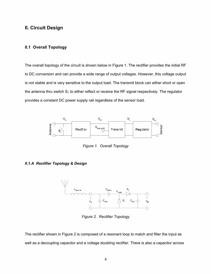
The overall topology of the circuit is shown below in Figure 1. The rectifier provides the initial RF
to DC conversion and can provide a wide range of output voltages. However, this voltage output
is not stable and is very sensitive to the output load. The transmit block can either short or open
the antenna thru switch S1 to either reflect or receive the RF signal respectively. The regulator
provides a constant DC power supply rail regardless of the sensor load.
Sen
sor
Ant
enna
Figure 1. Overall Topology
II.1.A Rectifier Topology & Design
Figure 2. Rectifier Topology
The rectifier shown in Figure 2 is composed of a resonant loop to match and filter the input as
well as a decoupling capacitor and a voltage doubling rectifier. There is also a capacitor across

5
the rectifier to low-pass filter and smooth the rectified output. The tuning capacitor is sized to
resonate with the inductance of the antenna by using equation 1 where f is the frequency of
operation and Lantenna and Ctune are taken from Figure 2.
tuneantenna CLf
*12 =π 1
Cclamp and D1 form the negative clamp while Crect and D2 form the peak rectifier. The negative
clamp serves to raise the average sine wave voltage by preventing Vclamp from going below
negative one diode drop (~-0.7 V). Thus, a sine wave at the input with an amplitude of 2 V
resulting from the LC resonator at VA would look like a sine wave with a range from -0.7 V to
3.3 V at Vclamp. It should be noted that a sine wave with an amplitude less than -0.7 V would
never turn D1 on, and thus would not be affected by the clamp circuit. The peak rectifier takes
this sine wave and converts it to a DC signal that is equal to the highest voltage minus one
diode drop. So, from the previous example the 2 V amplitude wave would have a resulting 2.6 V
rectified output. These signals can be seen below in Figure 3. It should again be noted that if the
input since wave has an amplitude less than 0.7 V, D2 will never turn on and the voltage output
will be zero volts.
Figure 3. Rectifier Output Waveforms
6
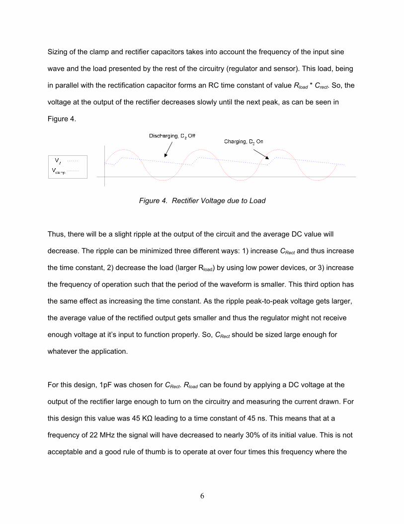
Sizing of the clamp and rectifier capacitors takes into account the frequency of the input sine
wave and the load presented by the rest of the circuitry (regulator and sensor). This load, being
in parallel with the rectification capacitor forms an RC time constant of value Rload * Crect. So, the
voltage at the output of the rectifier decreases slowly until the next peak, as can be seen in
Figure 4.
Figure 4. Rectifier Voltage due to Load
Thus, there will be a slight ripple at the output of the circuit and the average DC value will
decrease. The ripple can be minimized three different ways: 1) increase CRect and thus increase
the time constant, 2) decrease the load (larger Rload) by using low power devices, or 3) increase
the frequency of operation such that the period of the waveform is smaller. This third option has
the same effect as increasing the time constant. As the ripple peak-to-peak voltage gets larger,
the average value of the rectified output gets smaller and thus the regulator might not receive
enough voltage at it’s input to function properly. So, CRect should be sized large enough for
whatever the application.
For this design, 1pF was chosen for CRect. Rload can be found by applying a DC voltage at the
output of the rectifier large enough to turn on the circuitry and measuring the current drawn. For
this design this value was 45 KΩ leading to a time constant of 45 ns. This means that at a
frequency of 22 MHz the signal will have decreased to nearly 30% of its initial value. This is not
acceptable and a good rule of thumb is to operate at over four times this frequency where the
7
value has only decreased by 2%. For this design therefore, one should only operate above 88
MHz. For more details on the rectifier design, see pages 185 to 197 of [4].
II.1.A.i Rectifier Transistor Choice
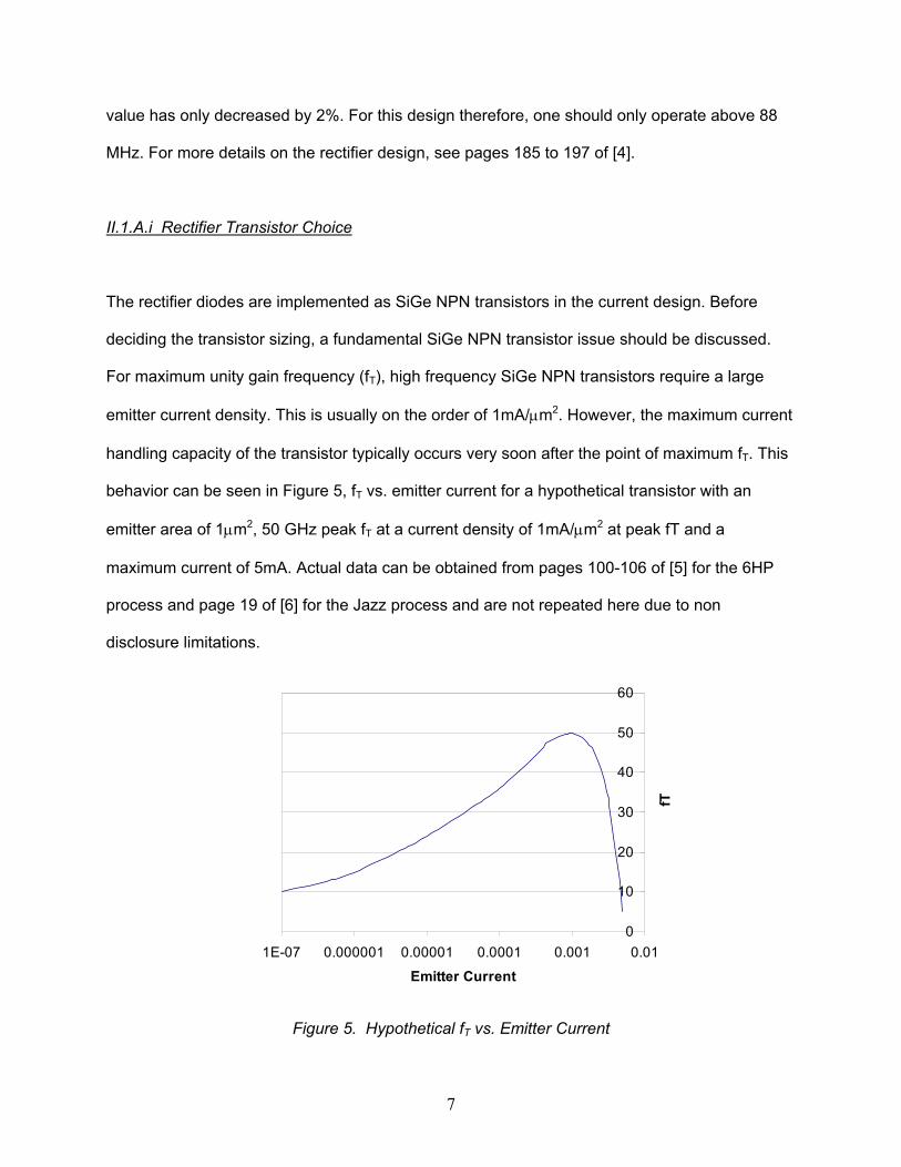
The rectifier diodes are implemented as SiGe NPN transistors in the current design. Before
deciding the transistor sizing, a fundamental SiGe NPN transistor issue should be discussed.
For maximum unity gain frequency (fT), high frequency SiGe NPN transistors require a large
emitter current density. This is usually on the order of 1mA/µm2. However, the maximum current
handling capacity of the transistor typically occurs very soon after the point of maximum fT. This
behavior can be seen in Figure 5, fT vs. emitter current for a hypothetical transistor with an
emitter area of 1µm2, 50 GHz peak fT at a current density of 1mA/µm2 at peak fT and a
maximum current of 5mA. Actual data can be obtained from pages 100-106 of [5] for the 6HP
process and page 19 of [6] for the Jazz process and are not repeated here due to non
disclosure limitations.
0
10
20
30
40
50
60
1E-07 0.000001 0.00001 0.0001 0.001 0.01
Emitter Current
fT
Figure 5. Hypothetical fT vs. Emitter Current

8
Therefore, for maximum frequency of operation we should operate the transistors as close to
their maximum unity gain point as possible. If the load of the rectifier is well known, we may size
the transistors such that they yield a peak fT and the rectifier will be operable at very high
frequencies. If the load is unknown, the transistor should be sized large enough such that the
maximum current that can be delivered to the load does not exceed the transistors maximum
current handling capacity. The size of the capacitors does not affect this frequency dependency
because if the transistors cannot supply enough charge each cycle, the rectified voltage will
drop regardless of the charge capacity of the circuit.
II.1.B Regulator Topology & Design
The regulator shown in figure 6 was chosen for its high over-current protection and low internal
power dissipation. It is composed of a Bandgap voltage source to provide the reference voltage,
an Operational Amplifier to servo the Bandgap voltage (VRef) to a resistor chain (VX), and a
PMOS pass transistor to compensate for different loads. Sizing the resistor chain according to
equation 2 can give any value of VD necessary at the output of the regulator (and the entire RF-
DC converter), given that the rectified voltage will be higher than the final VD. If the OpAmp has
enough gain, the voltage VRef will appear at VX. VD may be found by a voltage divider equation.
For this design a VD of 3.0 Volts was chosen.
+=→
+=
2
1fRe
21
2 1*R
RD
RR
RDX R
RVV
RRR
VV 2

9
Bandgap RR1
RR2
OpAmp
QPass
VRef
VX
+
VC
-
VG +
VD
-
Figure 6. Regulator
There is a fundamental tradeoff between the area of QPass and maximum available current. The
larger the transistor, the more current it can source without driving the OpAmp output into a non-
linear region. Equation 3 shows the relationship between the current and the voltage from gate
to source (VGS).
( ) ( )CDTGSoxn
D VVVVLWC
i −−≅ *2
µ 3
As the current increases, the voltage from gate to source increases. Since the source is at a
fixed potential the gate voltage drops, thus driving the output of the OpAmp lower and lower.
When this output reaches the low end of the output swing rang of the OpAmp, it no longer
functions in a linear manner and the regulator cannot increase the current to the load beyond
this limit. For this design, the maximum current was set to 1mA with a size of W/L = 60 / 0.5.
Another way to think of the tradeoff between area and current is by examining the relationship
between the resistance of QPass and its VGS. A larger current requires a smaller resistance in
order to maintain the same VDS. As can be seen from equation 4 (resistance from drain to
source of a transistor in deep triode), the smaller the resistance, the larger VGS must be.

10
( )TGSoxn
DS
VVLWC
R−
=µ
1 4
II.1.C Bandgap Topology & Design
The bandgap reference as shown in figure 7 is designed to provide a constant voltage of 1.18V
regardless of temperature variations and is inspired by a bandgap topology by Rincon-Mora [7].
Semiconductor physics states that if two bipolar transistors operate at unequal current densities,
then the difference of their base-emitter voltages is equal to VT * ln ∆IS (current density ratio).
Thus, while the base to emitter voltage of each transistor decreases with temperature their
difference is proportional to absolute temperature (from p382-3 of [8]).
Figure 7. Bandgap Reference

11
In this topology, this difference appears across resistor RPTAT. Since the resistance value of a
resistor increases with temperature according to equation 5, the resulting current (voltage
divided by resistance RPTAT) will be constant regardless of temperature. This current is mirrored
such that the current through RPTAT2 is constant as well. The voltage across RPTAT2 therefore
increases with temperature while the voltage from emitter to base of QN2 decreases. Since the
output voltage is equal to these two voltages added together it remains constant through
temperature changes.
)(** CTTCRR oNOM= 5
RPTAT is sized by equation 6 where C is the ratio of the size of QN3 to QN2 (∆IS) and IPTAT is a
current that is chosen by the designer. The current should be chosen as a tradeoff between
power consumption and output current. Since a requirement of the bandgap operation is for
equal current flow through both QN2 and QN3 the output current must be negligible compared to
IPTAT. The value of C is chosen as a tradeoff between area and reliability. Large values mean a
large area for QN3, however a deviation in the value of C will have less impact than if the same
deviation appeared with a smaller value of C. For the design presented in this report a value of
5.4 KΩ was chosen as RPTAT for a current of 10µA and a ratio of 8 between the transistors.
RPTAT2 is chosen by equation 7 and is 13.5 KΩ in this design.
PTATPTAT I
CVtR ln*= 6

12
PTAT
QNBEPTAT I
VVR
*32fRe
2−−
= 7
The turn-on voltage of this topology is obtained from equation 8 (where saturation voltage for a
MOSFET is equal to ∆VGS). From this equation we see a direct relationship between the sizes of
both the mirror transistors as well as the cascode transistors. Increasing the sizes (W/L ratio) of
either of these transistors yields a lower turn-on voltage. For the sizing of W/L = 1/1 for this
design, at a current of 10µA, the turn-on voltage is designed to be 2.6 Volts.
REFcasc
casc
oxn
D
mirror
mirror
oxn
DREFSatDSSatDSOnTurn V
WL
CI
WL
CI
VcascVmirrorVV ++=++= −−− *2
*2
)()(µµ
8
The cascode transistors are an optional addition and are added to shield the PFET current
mirror transistors from large voltages output from the large rectifier voltage. In the SiGe 6HP
process used, this would enable a working voltage up to approximately 6.6 V (equation 9 with
Vbreak-down = 2.7 V from [5]), as opposed to 4 V (equation 9 with only one breakdown voltage) if
they were not added. Another approach would have been to use higher break-down voltage
transistors (up to 3.5 V in this process). CStable (the capacitor connected to the base of QN1) is
used to stabilize the input voltage to that transistor and should be sized through circuit
simulation. Finally, the startup transistor Qstartup is chosen to have a very small W/L in order to
take as little current away from QN1 as possible. For this design W/L is chosen to be 1/5.
downbreakREFMax VVV −+= *2 9

13
The bandgap is extremely sensitive to resistive loading, as the nominal current through each
branch is only 10µA. Since there is a current mirror driving each branch, if any DC current is
used to drive an output it will starve QN3 of current, causing the circuit to malfunction. In order to
minimize this sensitivity one could increase the current in each branch, thus increasing the load
current necessary to cause failure. In this design, the bandgap drives a FET input, and thus can
operate on a very low current level (10µA).
II.1.D Opamp Topology & Design
The specifications for the OpAmp need not be very high for this application so a standard one
stage Opamp with a gain of over 60dB was designed (see figure 8). This reduces the number of
poles and aids in assuring stability. Since the circuit operates at low frequencies, bandwidth is
not a large consideration. The bias is provided by the bandgap reference to ensure reliable
performance under temperature variations. Power and area were minimized such that the
design uses 150µA and is approximately 120µm2.
Figure 8. Opamp

14
The turn-on voltage for the Opamp is given by a similar equation to equation 8 and is equal to
2.7 Volts. The output swing is equal to VDS-SAT of QPOp2 at the high end and the summation of
VDS-SAT of the lower three NFET transistors. This becomes a swing of 0.6 V to (VD – 0.3) V.
II.1.E Transmission
Data transmission is accomplished by either shorting or opening the antenna and having the
external RF source look at the reflected radiation. This is accomplished via a bipolar switch
which either shorts the antenna or allows power to be drawn into the circuit. An MOS switch is
also present, stopping the charging of storage capacitors CClamp and CRect (from Figure 2) for the
reflection case or keeping the antenna open and continuing to charge the storage capacitor in
the other case. Shown below is the schematic of the transmission circuit. It connects in series
between the rectifier and regulator and will generally just pass the rectifier voltage to the
regulator when Vtransmit is low. Inverters INV1 and INV2 serve as a buffer between the electronics
(which may not be able to supply enough current to turn on QS1) and the switch S1.
VTransmit
QTransmit
+
VB
-
+
VC
-QS1
RS1
S1
VA
INV1 INV2
Figure 9. Transmission Circuit

15
II.2 Chip Layout & Extraction
II.2.A Layout
The layout of the circuit is shown in Figure 10. The pads are shown on the outside with the
circuitry in the lower left. The pads correspond to Vtransmit, Vbandgap, GND and VD from left to right.
The total area is 650µm by 450µm.
(A) (B)
Figure 10. Layout of RF to DC circuit (A) Micrograph (B)
The entire chip is shown in Figure 11. There are two copies of the antenna + circuitry, laid out in
opposite directions of each other. They are nearly identical with the difference being the circuit
on the left does not include the shunt switch (Note that there are only three pads- there is no
need for Vtransmit).
Figure 11. Micrograph of entire chip

16
II.2.B Ground Connection
Figure 12. Mistake in Ground Connection
A mistake was made during layout in the ground connection of the chip. Instead of connecting
the ground pad directly to the on-chip ground of the circuit, the two are connected ‘thru’ the
substrate via substrate connections on both the pad and the on-chip ground line (see Figure
12). This essentially adds a resistive path between the two which is a combination of the
resistance through the substrate contacts and then through the substrate itself. The value of the
substrate contact resistance is approximately 40 Ohms, which is an extracted value from the
netlist (the netlist gives information about the size of the substrate contact and by creating a
separate schematic with that substrate contact in parallel to a voltage source, resistance may be
found by measuring the current through the contact). The resistance through the substrate is not
currently known due to the fact that substrate resistivity information could not be found in any of
the documents available through the Carnegie Mellon MEMS Lab. However, as it is
characterized as a low resistance substrate, the value is most likely of the same magnitude or
less than that of the substrate contact itself.
This added resistance has the effect of decreasing the power transferred to the circuit from the
signal source (HP signal generator or antenna, depending upon which test is being done). As
can be seen from figure 13, the amount of power transferred to a device from a 50 Ω source is
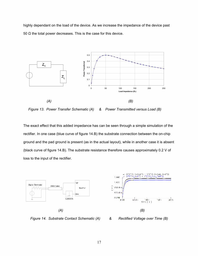
17
highly dependant on the load of the device. As we increase the impedance of the device past
50 Ω the total power decreases. This is the case for this device.
0
0.1
0.2
0.3
0.4
0.5
0 50 100 150 200 250Load Impedance (ZL)
Pow
er T
rans
ferr
ed
(A) (B)
Figure 13. Power Transfer Schematic (A) & Power Transmitted versus Load (B)
The exact effect that this added impedance has can be seen through a simple simulation of the
rectifier. In one case (blue curve of figure 14.B) the substrate connection between the on-chip
ground and the pad ground is present (as in the actual layout), while in another case it is absent
(black curve of figure 14.B). The substrate resistance therefore causes approximately 0.2 V of
loss to the input of the rectifier.
(A) (B)
Figure 14. Substrate Contact Schematic (A) & Rectified Voltage over Time (B)

18
II.2.C Extraction
Due to the long length of the antenna, there is much added capacitance to the input node of the
circuit. This changes the total input capacitance of the circuit from 90 fF to over 850 fF. This
changes the center frequency of operation due to the increased LC product at the input. This is
the most significant extracted parameter as most of the rest of the circuitry operates at DC
exclusively, so any added capacitance will yield better results (less noise and more stability).
These parasitics, though small, were used nonetheless during testing.
III. Simulation & Experimental Results
III.1 Simulation & Chip Testing Plan
Simulation of the circuit was completed with special attention paid to the testing model. As
stated previously (Section II.1.A) the circuit is inoperable at frequencies below 100MHz.
Standard probestations would not be able to be used for these high frequencies so an RF
probestation with high frequency Signal Generators and GSG probes was used. A model of this
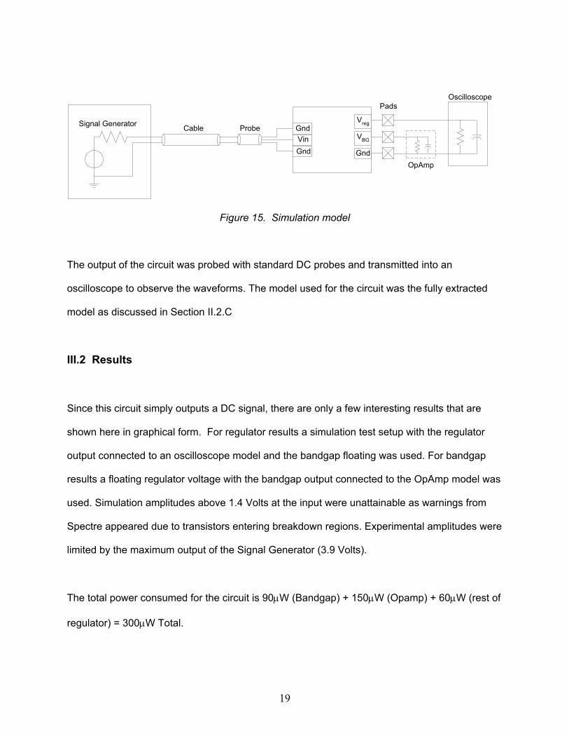
test setup was used to simulate the exact signal that would be present in the chip. It is shown in
figure 15 below. It includes a port model for the Signal Generator, transmission lines
representing the cable and probe, pad models for each probe pad and a resistor/capacitor for
each oscilloscope input. Since the bandgap is highly sensitive to any resistive loading (see
Section II.1.C) a JFET OpAmp with only a 250pA input bias was used in a basic buffer
configuration (input to positive terminal, output connected to negative terminal).
19
VinGnd
Signal Generator GndVreg
VBG
Gnd
Oscilloscope
Cable Probe
Pads
OpAmp
Figure 15. Simulation model
The output of the circuit was probed with standard DC probes and transmitted into an
oscilloscope to observe the waveforms. The model used for the circuit was the fully extracted
model as discussed in Section II.2.C
III.2 Results
Since this circuit simply outputs a DC signal, there are only a few interesting results that are
shown here in graphical form. For regulator results a simulation test setup with the regulator
output connected to an oscilloscope model and the bandgap floating was used. For bandgap
results a floating regulator voltage with the bandgap output connected to the OpAmp model was
used. Simulation amplitudes above 1.4 Volts at the input were unattainable as warnings from
Spectre appeared due to transistors entering breakdown regions. Experimental amplitudes were
limited by the maximum output of the Signal Generator (3.9 Volts).
The total power consumed for the circuit is 90µW (Bandgap) + 150µW (Opamp) + 60µW (rest of
regulator) = 300µW Total.
20
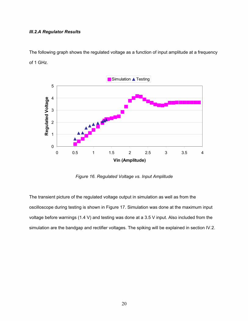
III.2.A Regulator Results
The following graph shows the regulated voltage as a function of input amplitude at a frequency
of 1 GHz.
0
1
2
3
4
5
0 0.5 1 1.5 2 2.5 3 3.5 4
Vin (Amplitude)
Reg
ulat
ed V
olta
ge
Simulation Testing
Figure 16. Regulated Voltage vs. Input Amplitude
The transient picture of the regulated voltage output in simulation as well as from the
oscilloscope during testing is shown in Figure 17. Simulation was done at the maximum input
voltage before warnings (1.4 V) and testing was done at a 3.5 V input. Also included from the
simulation are the bandgap and rectifier voltages. The spiking will be explained in section IV.2.
21
Figure 17. Transient regulator waveforms of simulation (A) and testing (B)
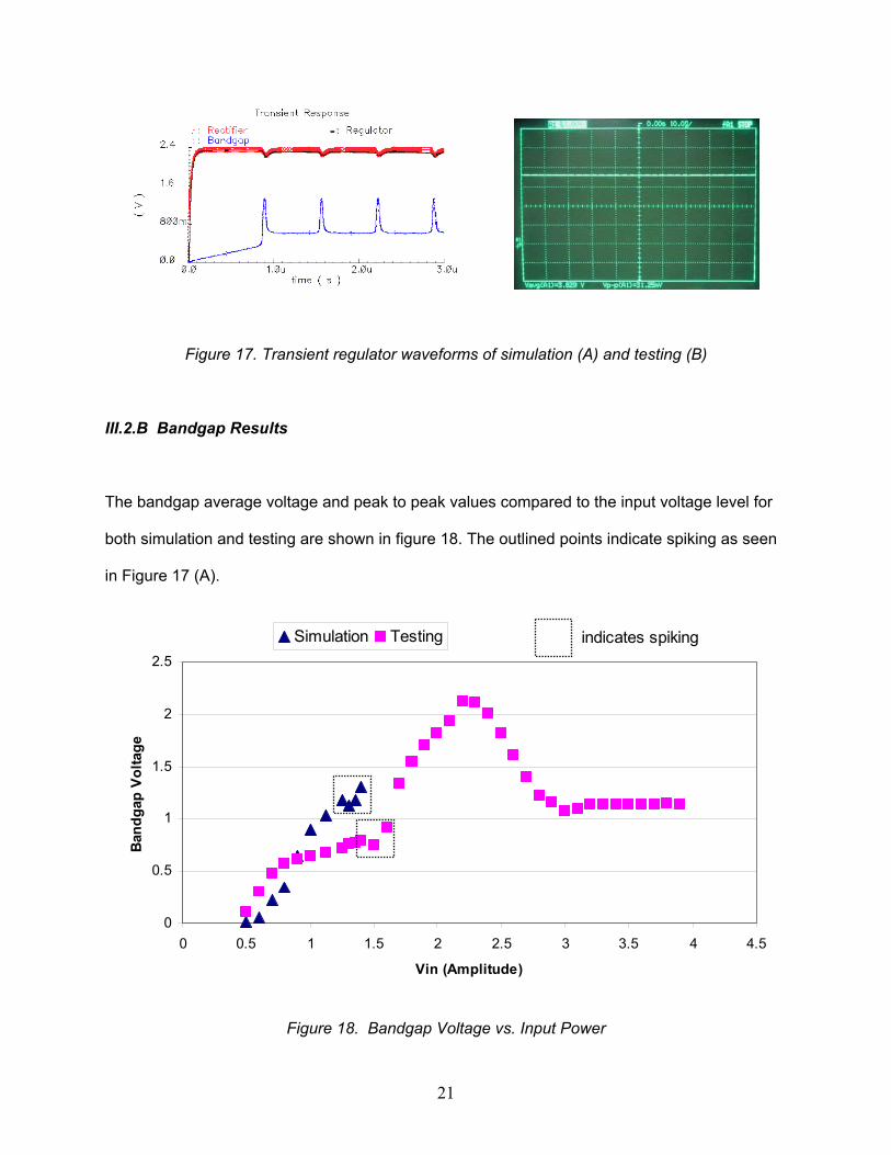
III.2.B Bandgap Results
The bandgap average voltage and peak to peak values compared to the input voltage level for
both simulation and testing are shown in figure 18. The outlined points indicate spiking as seen
in Figure 17 (A).
0
0.5
1
1.5
2
2.5
0 0.5 1 1.5 2 2.5 3 3.5 4 4.5
Vin (Amplitude)
Ban
dgap
Vol
tage
Simulation Testing indicates spiking
Figure 18. Bandgap Voltage vs. Input Power
22
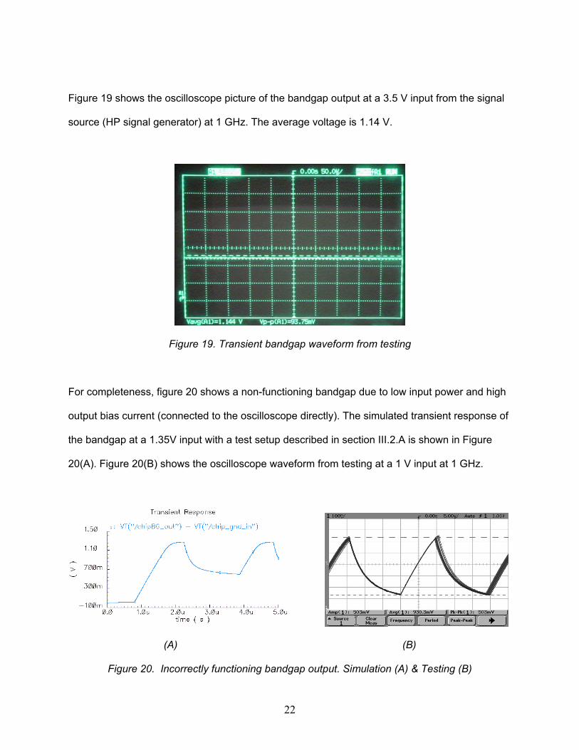
Figure 19 shows the oscilloscope picture of the bandgap output at a 3.5 V input from the signal
source (HP signal generator) at 1 GHz. The average voltage is 1.14 V.
Figure 19. Transient bandgap waveform from testing
For completeness, figure 20 shows a non-functioning bandgap due to low input power and high
output bias current (connected to the oscilloscope directly). The simulated transient response of
the bandgap at a 1.35V input with a test setup described in section III.2.A is shown in Figure
20(A). Figure 20(B) shows the oscilloscope waveform from testing at a 1 V input at 1 GHz.
(A) (B)
Figure 20. Incorrectly functioning bandgap output. Simulation (A) & Testing (B)

23
The theoretical voltage range of the bandgap is shown in Figure 21 below. This test is
conducted only at simulation level. Since there are no test structures for the bandgap by itself
on the chip.
Figure 21. Working Voltage range of Bandgap Circuit
IV. Assessment of Results
IV.1 Regulator Behavior
The regulator functioned well, outputting a DC value of 3.6 Volts over a range of input voltages.
This output value was higher than the expected 3.0 volts that the circuit was designed for. This
inconsistency can be attributed to resistor inaccuracy due to poor layout. One resistor was
divided into three series pieces at minimum spacing from each other, while the other was set as
one long piece with no polysilicon to either side. Furthermore, there were no dummy cells and
the resistors were laid out in a staggered fashion. This caused a large difference between the
two resistances, resulting in a higher than average regulated voltage. Figure 22 is a simplified
layout of these two resistors.

24
Figure 22. Resistor layout
IV.2 Bandgap Behavior
Two test setups were performed with the bandgap. The first contained a direct connection
between the bandgap output and the oscilloscope. The second test setup contained a buffer in
the form of a JFET OpAmp such that the bandgap output experiences much less loading.
Oscillation was seen in the first case (Figure 20.A). Spiking was seen in the second case
(Figure 17.A). Note that these two phenomena are only visible at low input voltages. As can be
seen from testing, at high enough voltages the bandgap operates normally.
The spiking bandgap voltages as seen in simulation and low-voltage testing are due to low input
voltages at the bandgap supply. As explained in Section II.1.A, under a load the rectifier
average DC value will decrease. When the circuit is first beginning to power-up the bandgap
does not draw any current and the rectified voltage increases to a steady level. Once the
bandgap begins to draw current and increase the output voltage, the rectified voltage drops due
to the sudden load. Once this voltage drops below the threshold voltage for bandgap power-up
the bandgap output drops and the rectifier voltage increases back to the steady level it was at

25
before. The cycle begins again once the bandgap tries to draw current, causing repetitive
spikes. At a high enough input voltage level the spiking goes away.
The oscillatory behavior that can be seen in figure 20 occurs when the JFET OpAmp buffer is
replaced by a direct connection to the oscilloscope. As in the spiking example, the bandgap tries
to power up but the decreasing rectifier voltage causes a drop in output voltage. The difference
in the oscilloscope case is that there is a load composed of a 9 pF capacitor and a 1 MΩ
resistor in parallel connected to the output. Since the transistors on the output of the circuit are
all in deep triode or are off due to the low voltages, the output must discharge through the
oscilloscope. This causes the behavior smooth charging and discharging seen in the results, as
compared with the crisp spiking seen with no bandgap load.
V. Conclusions
A functioning RF to DC converter to be used at RF frequencies is presented above. The output
from the regulator was higher than expected due to mismatch, but the bandgap output appeared
normal. The voltage range was constrained by the transistor breakdown voltages, leading to
cascading of devices and higher turn-on voltages. Problems were encountered during testing
due to simple mistakes during the pre-fabrication phase, including not shorting the ground pad
to the on-chip circuit ground and not matching the regulator resistor chain.

26
VI. Future Work
In order to meet voltage range requirements and ensure proper circuit performance a few steps
should be taken. Since the post-rectifier circuit is mainly one that operates at a DC value,
sacrificing high frequency performance for higher voltage range in the transistors should be a
top priority. Slower transistors will affect the startup time of the RF to DC conversion, but it will
allow much higher voltages without resorting to cascading, which can complicate a circuit.
Concerning the rectifier, not only should the transistors have large breakdown voltages but they
need to be large themselves. During the brief recharge period of each cycle a surge of current
must flow through the transistors. If the transistors aren’t large enough to handle this sudden
current they can breakdown or melt.
The circuit also suffered from poor layout design preventing circuit block testing. When the
circuit was fabricated no test structures such as a bandgap by itself or a regulator by itself were
present in the layout. This would have greatly aided in identifying problems and circuit
limitations. Also concerning the layout is the resistor and transistor matching. Dummy cells as
well as common gate and transistor widths should be present in the layout.

27
References
[1] H. Huang, et.al., “A 0.5mW Passive Telemetry IC”, IEEE Journal of Solid State Circuits,
July 1998.
[2] H. Marschner et. al, “A Modular Concept for the Design of Application Specific Integrated
Telemetric Systems” Proceedings of SPIE, Vol. 4408 (2001).
[3] K. Schuylenbergh and R. Puers, “Self Tuning Inductive Powering for Implantable Telemetric
Monitoring Systems”, 8th Conference of Solid-State Sensors and Actuators, June 1995.
[4] A. Sedra and K. Smith, Microelectronic Circuits, Oxford University Press, New York, NY
1998.
[5] IBM Corp., BiCMOS-6HP Model Reference Guide, Chapter 6, Version: November 15, 2001.
[6] Jazz Semiconductor, Jazz SiGe60 Electrical Parameters, Rev. 6.
[7] G. Rincon-Mora, Voltage References, IEEE Press, Piscataway, NJ, 2002.
[8] B. Razavi, Design of Analog CMOS Integrated Circuits, McGraw-Hill, New York, NY, 2001.