s-parameters
TRANSCRIPT
© H. Heck 2008 Section 5.5 1
Module 5: Advanced Transmission LinesTopic 5: 2 Port Networks & S-Parameters
OGI EE564
Howard Heck
© H. Heck 2008 Section 5.5 2
S-P
aram
eter
sEE 5
64
Where Are We?
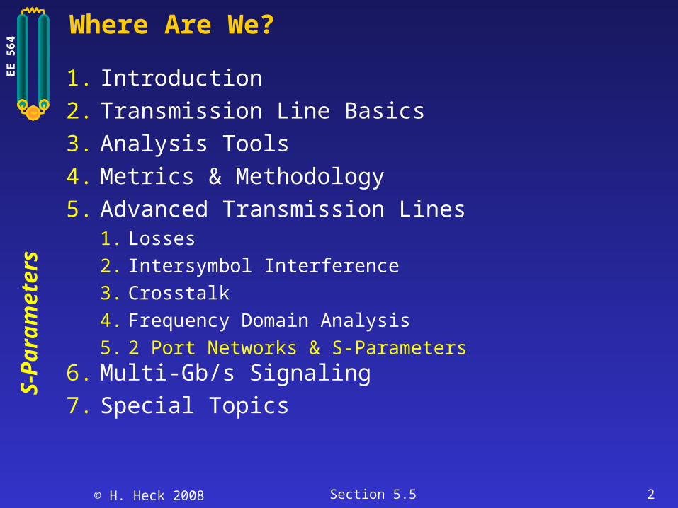
1. Introduction
2. Transmission Line Basics
3. Analysis Tools
4. Metrics & Methodology
5. Advanced Transmission Lines1. Losses
2. Intersymbol Interference
3. Crosstalk
4. Frequency Domain Analysis
5. 2 Port Networks & S-Parameters
6. Multi-Gb/s Signaling
7. Special Topics

© H. Heck 2008 Section 5.5 3
S-P
aram
eter
sEE 5
64
Acknowledgement
Much of the material in this section has been adapted from material developed by Stephen H. Hall and James A. McCall (the authors of our text).

© H. Heck 2008 Section 5.5 4
S-P
aram
eter
sEE 5
64
Contents
Two Port Networks Z Parameters Y Parameters Vector Network Analyzers S Parameters: 2 port, n ports Return Loss Insertion Loss Transmission (ABCD) Matrix Differential S Parameters (MOVE TO 6.2) Summary References Appendices

© H. Heck 2008 Section 5.5 5
S-P
aram
eter
sEE 5
64
Two Port Networks Linear networks can be completely characterized by
parameters measured at the network ports without knowing the content of the networks.
Networks can have any number of ports. Analysis of a 2-port network is sufficient to explain the theory
and applies to isolated signals (no crosstalk).
The ports can be characterized with many parameters (Z, Y, S, ABDC). Each has a specific advantage.
Each parameter set is related to 4 variables: 2 independent variables for excitation 2 dependent variables for response
2 PortNetworkP
ort
1I1
+
-
V1
Po
rt 2I2
+
-
V2

© H. Heck 2008 Section 5.5 6
S-P
aram
eter
sEE 5
64
Z Parameters
Advantage: Z parameters are intuitive. Relates all ports to an impedance & is easy to calculate.
Disadvantage: Requires open circuit voltage measurements, which are difficult to make. Open circuit reflections inject noise into measurements. Open circuit capacitance is non-trivial at high frequencies.
NNNNN
N
N I
I
I
ZZZ
Z
ZZZ
V
V
V
2
1
21
21
11211
2
1
IZV
0
jkI
j
iij I
VZ (Open circuit impedance)
Impedance Matrix: Z ParametersImpedance Matrix: Z Parameters
or [5.5.1]
where [5.5.2]
2221212
2121111
IZIZV
IZIZV
2 Port example:2 Port example:
2
1
2221
1211
2
1
I
I
ZZ
ZZ
V
V[5.5.4][5.5.3]

© H. Heck 2008 Section 5.5 7
S-P
aram
eter
sEE 5
64
Y Parameters
NNNNN
N
N V
V
V
YYY
Y
YYY
I
I
I
2
1
21
21
11211
2
1
VYI
0
jkV
j
iij V
IY (Short circuit admittance)
Admittance Matrix: Y ParametersAdmittance Matrix: Y Parameters
or
[5.5.6]
[5.5.5]
where
2221212
2121111
VYVYI
VYVYI
2 Port example:2 Port example:
2
1
2221
1211
2
1
V
V
YY
YY
I
I
Advantage: Y parameters are also somewhat intuitive. Disadvantage: Requires short circuit voltage
measurements, which are difficult to make. Short circuit reflections inject noise into measurements. Short circuit inductance is non-trivial at high frequencies.
[5.5.7] [5.5.8]

© H. Heck 2008 Section 5.5 8
S-P
aram
eter
sEE 5
64
Example
ZC
ZA ZB
+
-
+
-
V1 V2
I1 I2
Por
t 1
Por
t 2
CA
CAI
ZZ
ZZV
V
I
VZ
1
1
1
111
02
CC
I
ZI
ZI
I
VZ
2
2
2
112
01
CC
I
ZI
ZI
I
VZ
1
1
1
221
02
CB
CBI
ZZ
ZZV
V
I
VZ
2
2
2
222
01
© H. Heck 2008 Section 5.5 9
S-P
aram
eter
sEE 5
64
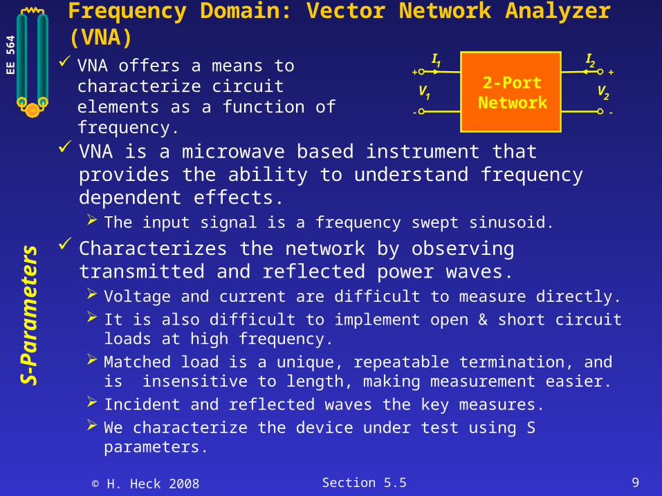
Frequency Domain: Vector Network Analyzer (VNA) VNA offers a means to
characterize circuit elements as a function of frequency.
VNA is a microwave based instrument that provides the ability to understand frequency dependent effects. The input signal is a frequency swept sinusoid.
Characterizes the network by observing transmitted and reflected power waves. Voltage and current are difficult to measure directly. It is also difficult to implement open & short circuit loads at high
frequency. Matched load is a unique, repeatable termination, and is
insensitive to length, making measurement easier. Incident and reflected waves the key measures. We characterize the device under test using S parameters.
2-PortNetwork
V1
+
V2
I1 I2
-
+
-

© H. Heck 2008 Section 5.5 10
S-P
aram
eter
sEE 5
64
S Parameters
We wish to characterize the network by observing transmitted and reflected power waves. ai represents the square root of the power wave injected into port i.
bi represents the square root of the power wave injected into port j.
2 PortNetwork
a1
+
-
V1
Po
rt 2
a2
+
-
V2
Po
rt 1
b1 b2
RVP
2
R
VPai
1
R
Vb jj
use
to get
[5.5.9]
[5.5.10]
[5.5.11]

© H. Heck 2008 Section 5.5 11
S-P
aram
eter
sEE 5
64
S Parameters #2
We can use a set of linear equations to describe the behavior of the network in terms of the injected and reflected power waves.
For the 2 port case:
2 PortNetwork
a1
+
-
V1
Po
rt 2
a2
+
-
V2
Po
rt 1
b1 b2
2221212
2121111
aSaSb
aSaSb
iport at measuredpower
jport at measuredpower
i
jij a
bSwhere
in matrix form:
[5.5.12]
[5.5.13]
2
1
2221
1211
2
1
a
a
SS
SS
b
b

© H. Heck 2008 Section 5.5 12
S-P
aram
eter
sEE 5
64
S Parameters – n Ports
[5.5.14]
[5.5.17]
n
nn Z
Va0
aSb
n
nn Z
Vb0
jkk
jkk
Vj
j
i
i
aj
iij
ZV
ZV
a
bS
,0
,0
0
0
nnnn
N
n a
a
a
SS
S
SSS
b
b
b
2
1
1
21
11211
2
1
nnnnnn
nn
nn
aSaSaSb
aSaSaSb
aSaSaSb
2211
22221212
12121111
or
[5.5.15]
[5.5.16]
[5.5.18]
© H. Heck 2008 Section 5.5 13
S-P
aram
eter
sEE 5
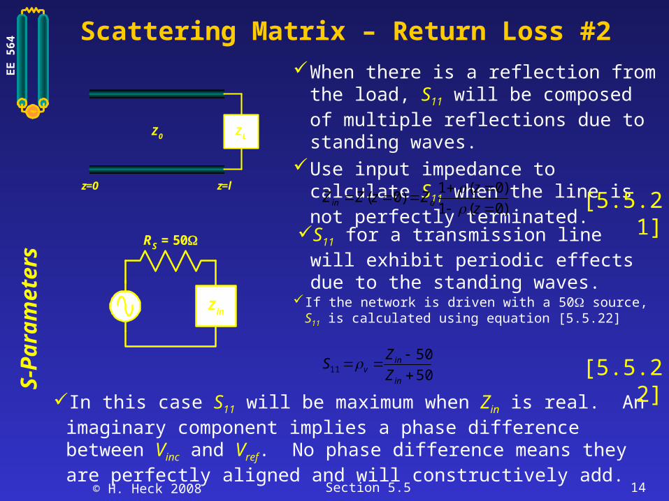
64 Scattering Matrix – Return Loss
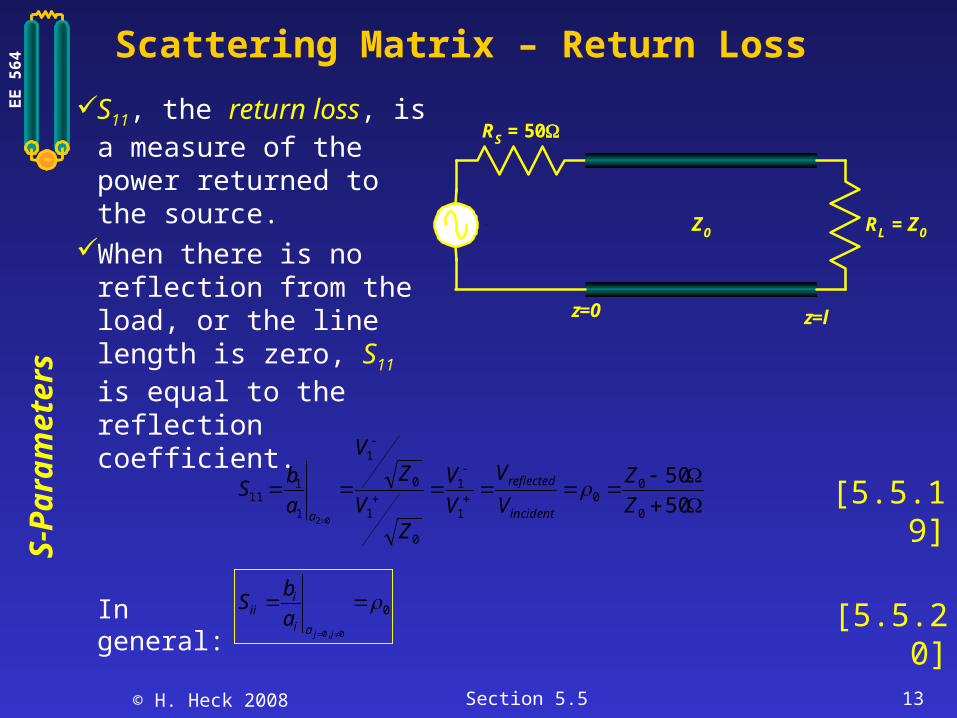
S11, the return loss, is a measure of the power returned to the source.When there is no
reflection from the load, or the line length is zero, S11 is equal to the reflection coefficient.
50
50
0
00
1
1
0
1
0
1
1
111
02Z
Z
V
V
V
V
ZV
ZV
a
bS
incident
reflected
a
[5.5.19]
RS = 50
RL = Z0Z0
z=0 z=l
0
0,0
jjai
iii a
bSIn general: [5.5.20]
© H. Heck 2008 Section 5.5 14
S-P
aram
eter
sEE 5
64 Scattering Matrix – Return Loss #2
When there is a reflection from the load, S11 will be composed of multiple reflections due to standing waves.
Use input impedance to calculate S11 when the line is not perfectly terminated.
)0(1
)0(1)0(
z
zZzZZ oin
If the network is driven with a 50 source, S11 is calculated using equation [5.5.22]
RS = 50
Zin
S11 for a transmission line will exhibit periodic effects due to the standing waves.
In this case S11 will be maximum when Zin is real. An imaginary component implies a phase difference between Vinc and Vref. No phase difference means they are perfectly aligned and will constructively add.
50
5011
in
inv Z
ZS
[5.5.21]
[5.5.22]
ZLZ0
z=lz=0

© H. Heck 2008 Section 5.5 15
S-P
aram
eter
sEE 5
64
Scattering Matrix – Insertion Loss #1
When power is injected into Port 1 and measured at Port 2, the power ratio reduces to a voltage ratio:
incident
dtransmitte
o
o
aV
V
V
V
Z
V
Z
V
a
bS
1
2
1
2
021
221
2 PortNetwork
a1
+
-
V1
Po
rt 2
a2
+
-
V2
Po
rt 1
b1 b2Z0 Z0
S21, the insertion loss, is a measure of the power transmitted from port 1 to port 2.
[5.5.22]

© H. Heck 2008 Section 5.5 16
S-P
aram
eter
sEE 5
64
Comments On “Loss”
True losses come from physical energy losses.Ohmic (i.e. skin effect) Field dampening effects (loss tangent) Radiation (EMI)
Insertion and return losses include other effects, such as impedance discontinuities and resonance, which are not true losses.
Loss free networks can still exhibit significant insertion and return losses due to impedance discontinuities.

© H. Heck 2008 Section 5.5 17
S-P
aram
eter
sEE 5
64
Reflection Coefficients
Reflection coefficient at the load:
0
0
ZZ
ZZ
L
LL
0
0
ZZ
ZZ
S
SS
L
L
L
Lin S
SS
S
SSS
11
212
1122
211211 11
S
Sout S
SSS
11
211222 1
[5.5.23]
[5.5.24]
[5.5.25]
[5.5.26]
Reflection coefficient at the source:
Input reflection coefficient:
Output reflection coefficient:
Assuming S12 = S21 and S11 = S22.

© H. Heck 2008 Section 5.5 18
S-P
aram
eter
sEE 5
64
Transmission Line Velocity Measurements
We can calculate the delay per unit length (or velocity) from S21:
S21 = b2/a1
p
d vlf
S 1
36021
Where (S21 ) is the phase angle of the S21 measurement.f is the frequency at which the measurement was taken.l is the length of the line.
[5.5.27]
Port 1 Port 2
a1
b1
a2
b2
0°180°
+90°
-90°
PositivePhase
NegativePhase
0.8 135°

© H. Heck 2008 Section 5.5 19
S-P
aram
eter
sEE 5
64
Impedance vs. frequency Recall
Zin vs f will be a function of delay () and ZL.
We can use Zin equations for open and short circuited lossy transmission.
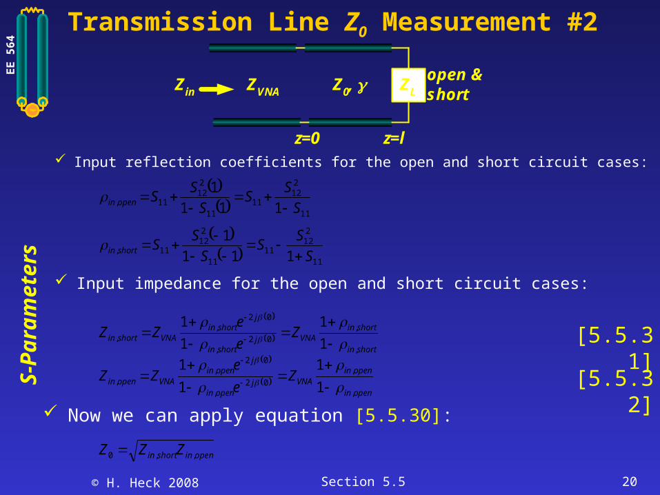
Transmission Line Z0 Measurements
lZZ openin tanh0,
lZZ shortin coth0,
lj
lj
in e
eZZ
2
2
0 1
1
openinshortin ZZZ ,,0
[5.5.28]
[5.5.29]
[5.5.30]
ZLZ0,
z=lz=0
Zin
ZLZ0,
z=lz=0
Zin
open &shortUsing the equation for Zin,
in, and Z0, we can find the impedance.
© H. Heck 2008 Section 5.5 20
S-P
aram
eter
sEE 5
64
Transmission Line Z0 Measurement #2
shortin
shortinVNAj
shortin
jshortin
VNAshortin Ze
eZZ
,
,
02,
02,
, 1
1
1
1
openinshortin ZZZ ,,0
[5.5.31]
[5.5.32]
11
212
1111
212
11, 111
1
S
SS
S
SSopenin
Input reflection coefficients for the open and short circuit cases:
11
212
1111
212
11, 111
1
S
SS
S
SSshortin
openin
openinVNAj
openin
jopenin
VNAopenin Ze
eZZ
,
,
02,
02,
, 1
1
1
1
Input impedance for the open and short circuit cases:
Now we can apply equation [5.5.30]:
ZLZ0,
z=lz=0
Zin
open &short
ZVNA
© H. Heck 2008 Section 5.5 21
S-P
aram
eter
sEE 5
64
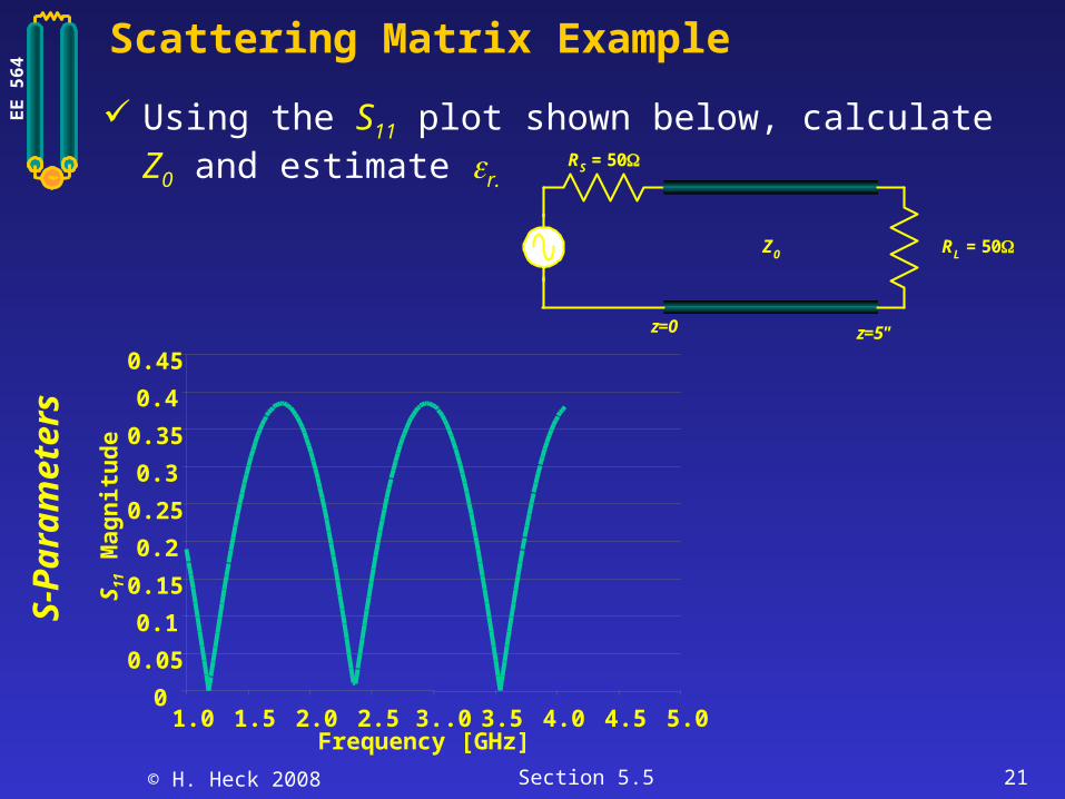
Scattering Matrix Example
Using the S11 plot shown below, calculate Z0 and estimate r.
01.0 1.5 2.0 2.5 3..0 3.5 4.0 4.5 5.0
Frequency [GHz]
0.05
0.1
0.15
0.2
0.25
0.3
0.35
0.4
0.45
S 11 M
agn
itu
de
RS = 50
Z0
z=0 z=5"
RL = 50
© H. Heck 2008 Section 5.5 22
S-P
aram
eter
sEE 5
64
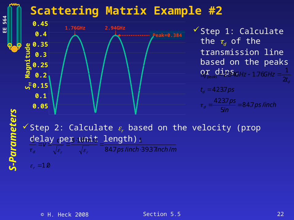
Scattering Matrix Example #21.76GHz 2.94GHz Step 1: Calculate the d
of the transmission line based on the peaks or dips.
dpeaks t
GHzGHzf2
176.194.2
Step 2: Calculate r based on the velocity (prop delay per unit length).
minchinchps
smcv
rrd /37.39/7.84
1/1031 8
Peak=0.384
0.05
0.1
0.15
0.2
0.25
0.3
0.35
0.4
0.45S 11
Mag
nit
ud
e
0.1r
pstd 7.423
inchpsin
psd /7.84
5
7.423
© H. Heck 2008 Section 5.5 23
S-P
aram
eter
sEE 5
64
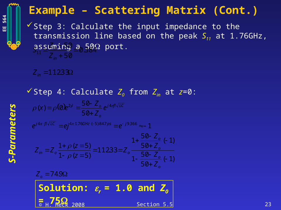
Example – Scattering Matrix (Cont.)Step 3: Calculate the input impedance to the transmission line
based on the peak S11 at 1.76GHz, assuming a 50 port.
384.050
5011
in
in
Z
ZS
Step 4: Calculate Z0 from Zin at z=0:
LCflj
o
ol eZ
Zex 42
50
500)(
Solution: r = 1.0 and Z0 = 75
33.112inZ
1366.97.84)5(76.144 jpsGHzLCflj eeje
)1(5050
1
)1(5050
1
33.112)5(1
)5(1
o
o
o
o
ooin
ZZZZ
Zz
zZZ
9.74oZ
© H. Heck 2008 Section 5.5 24
S-P
aram
eter
sEE 5
64
Advantages/Disadvantages of S Parameters
Advantages: Ease of measurement: It is much easier to measure
power at high frequencies than open/short current and voltage.
Disadvantages: They are more difficult to understand and it is more
difficult to interpret measurements.
© H. Heck 2008 Section 5.5 25
S-P
aram
eter
sEE 5
64
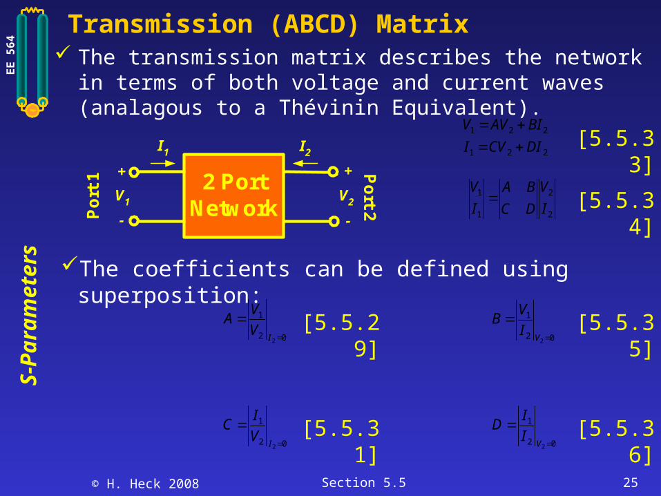
Transmission (ABCD) Matrix The transmission matrix describes the network in terms of
both voltage and current waves (analagous to a Thévinin Equivalent).
The coefficients can be defined using superposition:
221
221
DICVI
BIAVV
2
2
1
1
I
V
DC
BA
I
V
02
1
2
I
V
IC
2 PortNetwork
I1
+
-
V1
Po
rt 2
I2
+
-
V2
Po
rt 1
02
1
2
V
I
ID
02
1
2
V
I
VB
02
1
2
I
V
VA
[5.5.33]
[5.5.34]
[5.5.35]
[5.5.36]
[5.5.29]
[5.5.31]

© H. Heck 2008 Section 5.5 26
S-P
aram
eter
sEE 5
64
I1
+
-
V1
I2
V2
I1
I3
+
-
V3
Transmission (ABCD) Matrix
Since the ABCD matrix represents the ports in terms of currents and voltages, it is well suited for cascading elements.
The matrices can be mathematically cascaded by multiplication:
3
3
22
2
2
2
11
1
I
V
DC
BA
I
V
I
V
DC
BA
I
V
3
3
211
1
I
V
DC
BA
DC
BA
I
V
This is the best way to cascade elements in the frequency domain. It is accurate, intuitive and simple to use.
2DC
BA
1DC
BA
[5.5.37]

© H. Heck 2008 Section 5.5 27
S-P
aram
eter
sEE 5
64
ABCD Matrix Values for Common Circuits
ZPort 1 Port 2 10
1
DC
ZBA
Port 1 Y Port 2 1
01
DYC
BA
323
3212131
/1/1
//1
ZZDZC
ZZZZZBZZA
Z1
Port 1 Port 2
Z2
Z3
Y1Port 1 Port 2Y2
Y3
3132121
332
/1/
/1/1
YYDYYYYYC
YBYYA
Port 1 Port 2,oZ)cosh()sinh()/1(
)sinh()cosh(
lDlZC
lZBlA
o
o
l
[5.5.38]
[5.5.39]
[5.5.40]
[5.5.41]
[5.5.42]
© H. Heck 2008 Section 5.5 28
S-P
aram
eter
sEE 5
64
Converting to and from the S-Matrix
The S-parameters can be measured with a VNA, and converted back and forth into ABCD the Matrix Allows conversion into a more intuitive matrix Allows conversion to ABCD for cascading ABCD matrix can be directly related to several useful circuit
topologies
© H. Heck 2008 Section 5.5 29
S-P
aram
eter
sEE 5
64
Po
rt 2
Po
rt 1
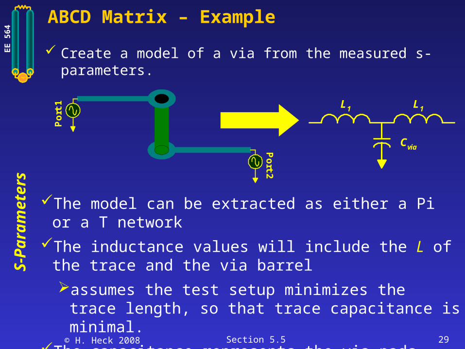
ABCD Matrix – Example
Create a model of a via from the measured s-parameters.
The model can be extracted as either a Pi or a T network
The inductance values will include the L of the trace and the via barrel
assumes the test setup minimizes the trace length, so that trace capacitance is minimal.
The capacitance represents the via pads.
L1 L1
Cvia

© H. Heck 2008 Section 5.5 30
S-P
aram
eter
sEE 5
64
ABCD Matrix – Example #1 The measured S-parameter matrix at 5 GHz is:
153.0110.0572.0798.0
572.0798.0153.0110.0
2221
1211
jj
jj
SS
SS
Converted to ABCD parameters:
827.00157.0
08.20827.0
2
11
2
112
11
2
11
21
21122211
21
21122211
21
21122211
21
21122211
j
j
S
SSSS
SZ
SSSSS
SSSSZ
S
SSSS
DC
BA
VNA
VNA
Relating the ABCD parameters to the T circuit topology, the capacitance can be extracted from C & inductance from A:
pFC
fCjZ
jC VIA
VIA
5.0
2111
0157.03
nHLLfCj
fLj
Z
ZA
VIA
35.0)2/(1
21827.01 21
3
1
Z1
Port 1 Port 2
Z2
Z3

© H. Heck 2008 Section 5.5 31
S-P
aram
eter
sEE 5
64
Advantages/Disadvantages of ABCD Matrix
Advantages: The ABCD matrix is intuitive: it describes all ports with
voltages and currents. Allows easy cascading of networks. Easy conversion to and from S-parameters. Easy to relate to common circuit topologies.
Disadvantages: Difficult to directly measure: Must convert from
measured scattering matrix.

© H. Heck 2008 Section 5.5 32
S-P
aram
eter
sEE 5
64
Summary
We can characterize interconnect networks using n-Port circuits.
The VNA uses S- parameters.From S- parameters we can characterize
transmission lines and discrete elements.

© H. Heck 2008 Section 5.5 33
S-P
aram
eter
sEE 5
64
References D.M. Posar, Microwave Engineering, John Wiley & Sons,
Inc. (Wiley Interscience), 1998, 2nd edition. B. Young, Digital Signal Integrity, Prentice-Hall PTR, 2001,
1st edition. S. Hall, G. Hall, and J. McCall, High Speed Digital System
Design, John Wiley & Sons, Inc. (Wiley Interscience), 2000, 1st edition.
W. Dally and J. Poulton, Digital Systems Engineering, Chapters 4.3 & 11, Cambridge University Press, 1998.
“Understanding the Fundamental Principles of Vector Network Analysis,” Agilent Technologies application note 1287-1, 2000.
“In-Fixture Measurements Using Vector Network Analyzers,” Agilent Technologies application note 1287-9, 2000.
“De-embedding and Embedding S-Parameter Networks Using A Vector Network Analyzer,” Agilent Technologies application note 1364-1, 2001.

© H. Heck 2008 Section 5.5 34
S-P
aram
eter
sEE 5
64
Appendix
More material on S parameters.

© H. Heck 2008 Section 5.5 35
S-P
aram
eter
sEE 5
64
0Re
any for 0Re
mn
mn
Y
m,nZ
jkkIj
iij I
VZ
,0
jkkVj
iij V
IY
,0
Lossless
Reciprocal jiij ZZ jiij ZZ
1 ZY

© H. Heck 2008 Section 5.5 36
S-P
aram
eter
sEE 5
64
S Parameters
NNNNN
N
N V
V
V
SSS
S
SSS
V
V
V
2
1
21
12
12111
2
1
VSV
jkkV
j
iij V
VS
,0
Scattering Matrix: S ParametersScattering Matrix: S Parameters
or [5.5.1]
where [5.5.2]
nnn VVV
nnnnn VVIII ???? VVVIZIZIZ
VUZVUZ
10
10
001
U
UZUZVVS 11

© H. Heck 2008 Section 5.5 37
S-P
aram
eter
sEE 5
64
S Parameters #2
[5.5.1]
where [5.5.2]
UZUZVVS 11
USZSUZUZS
SUSUZ 1
TSS Reciprocal
N
kkikiSS
1
* 1
N
kkjki jiSS
1
* ,0

© H. Heck 2008 Section 5.5 38
S-P
aram
eter
sEE 5
64
S Parameters – n Ports
[5.5.1]
[5.5.2]
n
nn Z
Va0
aSb
n
nn Z
Vb0
nnnnnn baZVVV 0
nn
nn
nnn ba
ZZ
VVI
00
1
22
2
1
2
1nnn baP
jkkaj
iij a
bS
,0
jkk
jkk
Vj
j
i
i
aj
iij
ZV
ZV
a
bS
,0
,0
0
0
nnnn
N
n a
a
a
SS
S
SSS
b
b
b
2
1
1
21
11211
2
1
nnnnnn
nn
nn
aSaSaSb
aSaSaSb
aSaSaSb
2211
22221212
12121111

© H. Heck 2008 Section 5.5 39
S-P
aram
eter
sEE 5
64
S Parameters #4
[5.5.1]
[5.5.2]
aSb
where
jkkaj
iij a
bS
,0
jkk
jkk
Vj
j
i
i
aj
iij
ZV
ZV
a
bS
,0
,0
0
0
niaSbn
jjiji ,,3,2,1for
Sij = ij is the reflection coefficient of the ith port if i=j with all other ports matched
Sij = Tij is the forward transmission coefficient of the ith port if I>j with all other portsmatched
Sij = Tij is the reverse transmission coefficient of the ith port if I<j with all other portsmatched
© H. Heck 2008 Section 5.5 40
S-P
aram
eter
sEE 5
64
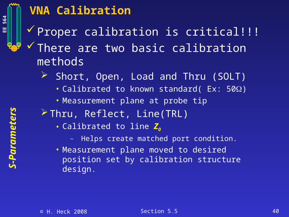
VNA Calibration
Proper calibration is critical!!!There are two basic calibration methods Short, Open, Load and Thru (SOLT)
• Calibrated to known standard( Ex: 50)• Measurement plane at probe tip
Thru, Reflect, Line(TRL)• Calibrated to line Z0
– Helps create matched port condition.
• Measurement plane moved to desired position set by calibration structure design.
© H. Heck 2008 Section 5.5 41
S-P
aram
eter
sEE 5
64
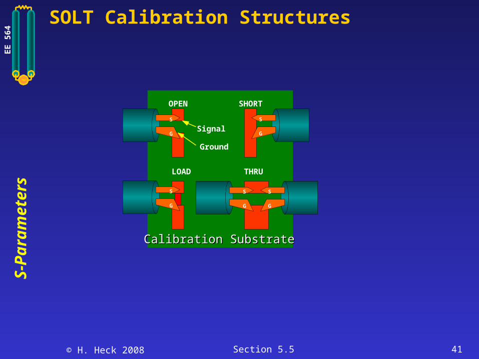
SOLT Calibration Structures
OPEN SHORT
LOAD THRU
Calibration SubstrateCalibration Substrate
G
G
S
S
G
S
Signal
Ground
G
S
G
S
© H. Heck 2008 Section 5.5 42
S-P
aram
eter
sEE 5
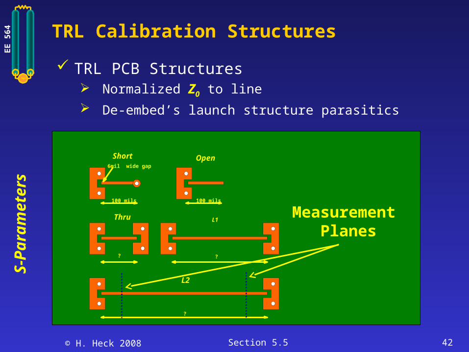
64 TRL Calibration Structures
TRL PCB Structures Normalized Z0 to line
De-embed’s launch structure parasitics
6mil wide gap
Short
100 mils 100 mils
Open
?
Thru
?
L1
?
L2
Measurement Planes
© H. Heck 2008 Section 5.5 43
S-P
aram
eter
sEE 5
64
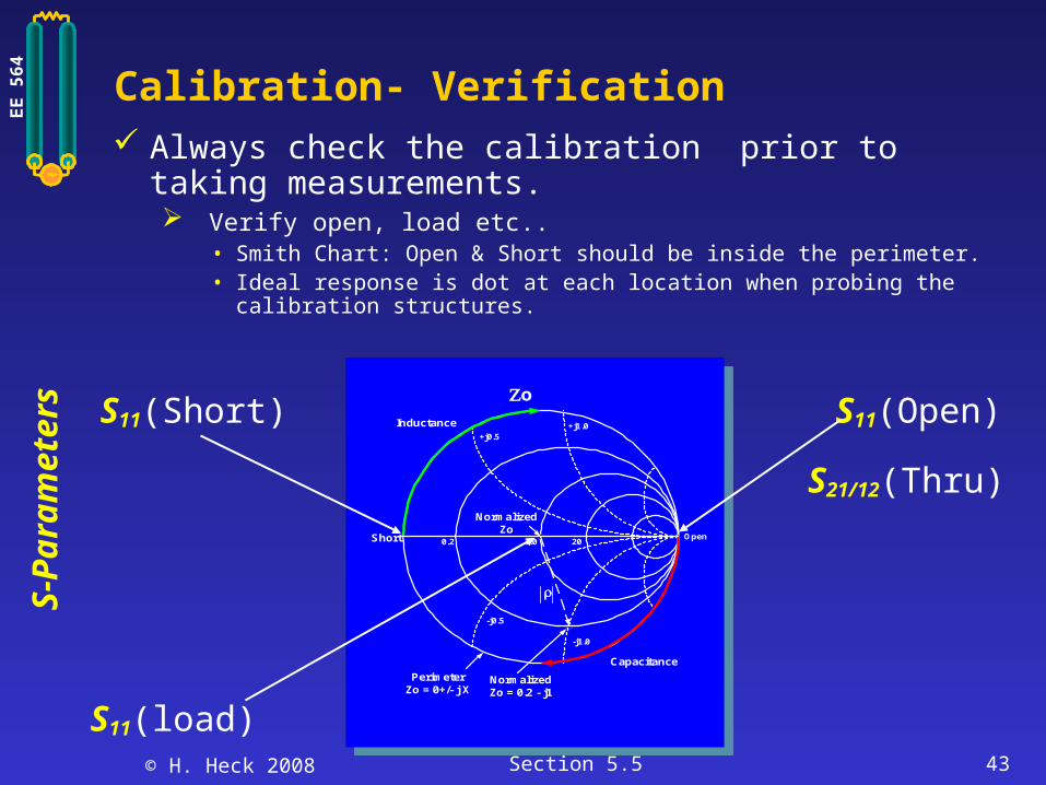
Calibration- Verification Always check the calibration prior to taking
measurements. Verify open, load etc..
• Smith Chart: Open & Short should be inside the perimeter.• Ideal response is dot at each location when probing the calibration
structures.
Capacitance
Inductance
NormalizedZo
PerimeterZo = 0+/- j X
Short 1.00.2 20
-j0.5
-j1.0
+j0.5+j1.0
Zo
Open
NormalizedZo = 0.2 - j1
Capacitance
Inductance
NormalizedZo
PerimeterZo = 0+/- j X
Short 1.00.2 20
-j0.5
-j1.0
+j0.5+j1.0
Zo
Open
NormalizedZo = 0.2 - j1
S11(Short) S11(Open)
S11(load)
S21/12(Thru)
© H. Heck 2008 Section 5.5 44
S-P
aram
eter
sEE 5
64
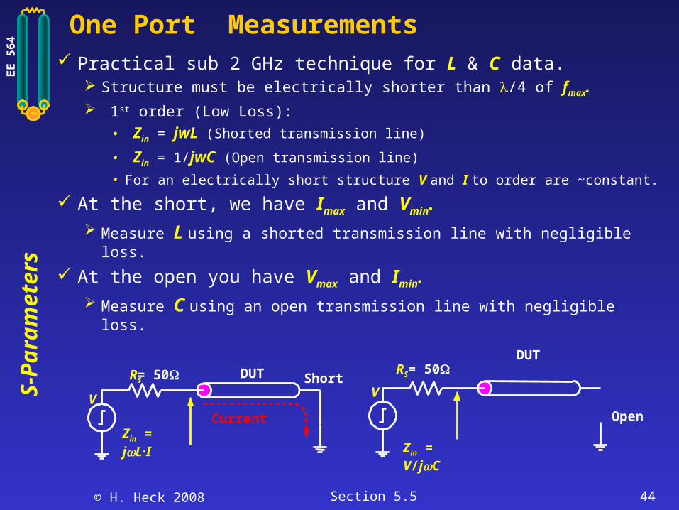
One Port Measurements Practical sub 2 GHz technique for L & C data.
Structure must be electrically shorter than /4 of fmax.
1st order (Low Loss):
• Zin = jwL (Shorted transmission line)
• Zin = 1/jwC (Open transmission line)
• For an electrically short structure V and I to order are ~constant.
At the short, we have Imax and Vmin. Measure L using a shorted transmission line with negligible loss.
At the open you have Vmax and Imin. Measure C using an open transmission line with negligible loss.
V
RS= 50 DUT Short
CurrentZin = jL·I
DUT
Open
V
RS = 50
Zin = V/jC

© H. Heck 2008 Section 5.5 45
S-P
aram
eter
sEE 5
64 One Port Measurements – L & C
VNA - Format Use Smith chart
format to read L & C data
Capacitance
Inductance
NormalizedZo
PerimeterZo = 0+/- j X
Short 1.00.2 20
-j0.5
-j1.0
+j0.5+j1.0
Zo
Open
NormalizedZo = 0.2 - j1
Capacitance
Inductance
NormalizedZo
PerimeterZo = 0+/- j X
Short 1.00.2 20
-j0.5
-j1.0
+j0.5+j1.0
Zo
Open
NormalizedZo = 0.2 - j1

© H. Heck 2008 Section 5.5 46
S-P
aram
eter
sEE 5
64
Connector L & C
Use test board to measure connector inductance and capacitance Measure values relevant to pinout Procedure
• Measure test board L & C without connector
• Measure test board with connector
• Difference = connector parasitics
Short Open