scam electric vehicle charger senior design 1 paper group
TRANSCRIPT

SCAM Electric Vehicle Charger
Senior Design 1 Paper
Group J
Name: Nathan Rodriguez, Edwin Lomans,
And Symone Adams
Spring 2016
Date: 4/28/15
Sponsor: Florida Solar Energy Center

Table of Contents
1. Abstract………………………………………………………………………………...1 2. Project Overview….............................................................................................2 2.1 Objective……………………………………………………………………………………2 2.2 Goals………………………………………………………………………………………..2 2.3 Description………………………………………………………………………………….2 3. Research……………………………………………………………………………….2 3.1 Communications…………………………………………………………………………...2
3.1.1 Origins of EVSE Charging Standards……..……...……….……………….2 3.1.2 SAE J1772 Protocols….…………………………………………………......3
3.1.2.1 Electrical Characteristics………….………………..……………....3 3.1.3 Electric Vehicle Charging Levels…….……………………………………...6
3.1.3.1 Level 1…………………………………………………………….…..6 3.1.3.2 Level 2……………………………………………………….………..7 3.1.3.3 Level 3……………………………………………………….………..7
3.1.4 Security………………………………………………………………..……….7 3.1.5 Information Communications Technology……………………………...….8
3.1.5.1 Wi-Fi…………………………………………………………………..8 3.1.5.2 Bluetooth………………………………………………..…………….9
3.1.6 Transceiver……………………………………………………………………9 3.1.6.1 Error Vector Magnitude………………………..……………………11 3.1.6.2 Electromagnetic Compatibility……………….…………………….11
3.2 Hardware……………………………………………………………………………………12 3.2.1 ADC………..……………………………………………………………..........12 3.2.2 Voltage Regulation……………………………………………………………13
3.2.2.1 Linear Regulator…………………………..………………………….14 3.2.2.2 Switching Regulator……………………………………………….…15
3.2.3 High Power Safety………………………………………………………….…16 3.2.4 EV Batteries……………………………………………………………………16
3.3 Application Software……………………………………………………………………….18 3.3.1 Hardware to Application……………………………………………………...18
3.4 Power Systems……………………………………………………………………………..19 3.4.1 Photovoltaic System………………………………………………………….19 3.4.2 Electrical Grid………………………………………………………………….19
3.5 Expansion…………………………………………………………………………………...19 3.5.1 PCI Express……………………………………………………………………20 3.5.2 Raspberry Pi 2…………………………………………………………………20
4. Standards……………………………………………………………………………….21 4.1 Power Supply……………………………………………………………………………….21 4.2 EV charging station…………………………………………………………………..…….21 4.3 Security………………………………………………………………………………..……22 4.4 Communication Protocols…………………………………………………………..........22
4.4.1 USB…………………………………………………………………………….22 4.4.2 SPI……………………………………………………………………………...22 4.4.3 UART………………………………………………………………………..…23 4.4.4 I2C………………………………………………………………………………23

4.5 Relevant Standards………………………………………………………………………..24 5. Project Description…………………………………………………………...…………………….25
5.1 Project Equipment…………………………………………………………………………25 5.1.1 Overall Description…………………………………………………… ……..25 5.1.2 Installation Hardware…………………………………………………………26 5.1.3 MCU……………………………………………………………………………26
5.1.3.1 MCU Selection……………………………………………………….26 5.1.3.2 MSP4305529 Features……………………………………………..29 5.1.3.3 MSP4305529 Low-Power Modules………………………………..30 5.1.3.4 Mixed-Signal Processor Monitoring………………………………..31 5.1.3.5 MCU Software Implementation……………………………………..34
5.1.3.5.1 Pin Configuration………………………………………..34 5.1.3.5.2 Power Management Module………………….............35 5.1.3.5.3 Timer-B Configuration…………………………..………35 5.1.3.5.4 ADC Configuration………………………………………35 5.1.3.5.5 Flash Configuration..……………………………………35
5.1.3.6 MSP Clock Functions………………………………………………..36 5.1.3.7 SPI MCU to RC System……………………………………………..39 5.1.3.8 UART MCU to RC System…………………………………………..40
5.1.4 Transceiver…………………………………………………………………….40 5.1.4.1 SPI RC System to MCU……………………………………………..41 5.1.4.2 UART RC System to MCU………………………………………...,.43 5.1.4.3 Compatibility…………………………………………………………..45 5.1.4.4 API’s……………………………………………………………………45 5.1.4.5 Network Application………………………………………………….45
5.1.4.5.1 Design……………………………………………………47 5.1.4.6 Security……………………………………………………………….48 5.1.4.7 Software Application…………………………………………………50
5.1.4.7.1 Programming…………………………………………….51 5.1.4.8 Provisioning…………………………………………………………..51
5.1.5 Power Connection…………………………………………………………….52 5.1.5.1 Grid…………………………………………………………………….52 5.1.5.2 Vehicle…………………………………………………………………52
5.1.6 User Interface……………………………………………………………... …53 5.1.7 Application Software………………………………………………………….54
5.1.7.1 Application Features…………………………………………………55 5.1.8 Raspberry Expansion…………………………………………………………56
5.1.8.1 Communication……………………………………………………….56 5.1.8.2 USB Configuration…………………………………………………...56
6. Design…………………………………………………………………………………………..56 6.1 Power Monitoring Circuit……………………………………………………………........56
6.1.1 PCB Layout Schematics……………………………………………….........57 6.1.2 FlowCharts…………………………………………………………………….57
6.2 MCU…………………………………………………………………………………………58 6.2.1 Communications Protocols…………………………………………………..59 6.2.2 AC/DC Conversion……………………………………………………………59 6.2.3 Keypad Functionality……………………………………………………........59
6.3 High Voltage Module Interface……………………………………………………………60 6.3.1 Requirements……………………………………………………………........60 6.3.2 Cables………………………………………………………………………….60 6.3.3 PCB Layout…………………………………………………………………….60

6.3.3.1 PCB Design Rules………………….…………………………….….61 6.3.3.2 Surface Finish…….…………………………………………………..62 6.3.3.3 Layer Finish…………………………………………………………...63 6.3.3.4 Layer Descriptions……………………………………………………63 6.3.3.5 Layout Details…………………………………………………………67
6.3.4 Noise Requirement……………………………………………………………69 6.4 RC Communications…………………………………………………………………….…70
6.4.1 Requirements……………………………………………………………….…70 6.4.2 Software Implementation………………………………………………….…74 6.4.3 Power Source………………………………………………………………….76 6.4.4 Electrical Connections………………………………………………………..76
6.5 External Housing…………………………………………………………………………..77 7. Testing…………………………………………………………………………………………..77
7.1 Radio communication TX.……………………………… ……………………………78 7.2 Radio communication Rx……………………………………………………………..79 7.3 Solder Joints……………………………………………………………………………80 7.4 Production Line testing RC System.…………………… ………………………..…81 7.5 MCU Controlled RF testing…………………………………………………………..81 7.6 PC Controlled RF testing……………………………………………………………..81 7.7 Access Point……………………………………………………………………………82
8. Constraints…………………………………………………………………………..………….82 8.1 Budget………………………………………………………………………………….82 8.2 Time…………………………………………………………………………………….82 8.3 Safety…………………………………….…………………………………………….83 8.4 Standards………………………………………………………………………………83
9. Group Dynamics………………………………………………………………………………..84 9.1 Work Distribution…………………………………………………………………………...84 9.2 Schedule……………………………………………………………………………………85
10. Budget…………………………………………………………………………………………...85 10.1 Funding…………………………………………………………………………………85 10.2 Bill of Materials…………………………………………………………………………86
11. List of Figures and Tables…………….……………………………………………………….91 12. Conclusion………………………………………………………………………………………93 13. Appendix………………………………………………………………………………………...94
13.1 Works Cited…………………………………………………………………………….94 14. Acknowledgements…………………………………………………………………………….95

1
1. Abstract/Executive Summary
With the landscape of Electric Vehicle (EV) use rising, it has become more necessary to increase the accessibility of Electric Vehicle charging stations at UCF. Due to the relatively new technology of owning an Electric Vehicle, charging stations had remained standard and ultimately inefficient. Having the charging station be capable of charging your vehicle in a timely manner has become increasingly more important, as well as utilizing the data specific qualities of the micro-controllers typically installed in them such as monitoring of power, energy, and connection time. Implementing security measures to limit non-UCF affiliation and up to date information of charge application without overly increasing the charge station production cost will allow for more EV charging stations to be allocated around campuses. When purchasing a new Electric Vehicle the user is outfitted with level-1 capable charging which consist of a cord for standard charging accessible with any standard three port 120 volt outlet. Level-1 charging initially the standard, however, has quickly become an obsolete form of powering your Electric Vehicle. Level-2 and Level-3 charging are quickly replacing the latter due to the dramatic ability to decrease charging times 10 fold. In a day and age where time and money are becoming the most valuable assets, it has become more imperative to find a balance between the two. Level-3 charging commonly known as DC fast charging is currently the fastest most efficient way to charge an Electric Vehicle implementing the use of a 480 volt circuit and a cord that inputs direct DC current into the vehicle. Where level-1 charging is considerably more time inefficient Level-3 charging can be extremely costly for the vehicle user as well as the charging station installer. Level-2 charging has become the balance between level-1 and level-3 charging as the user has to make minimal upgrades allowing considerably good time management returns and the production cost for the installer are relatively simple and cost efficient. Using a 240 volt circuit, the same used for high voltage house appliances such as a stove, a standard battery pack can be charged in as little as 3 hours from empty state. This will allow the University to allocate numerous charging stations around campus without incurring large financial obligations.
2. Project Overview 2.1 Objective
This project requires five integrated systems to allow for an Electric Vehicle safe charging intended for UCF affiliated personnel. These systems are a Power monitoring circuitry, a Mixed signal processor, a Transceiver wireless interface, a User interface module, and a High voltage cable interface module.
To ensure the stations can only be operated by active UCF students and staff internal programming will be implemented and synced to a mobile device by way of keypad entry accessible by NID password. A cellular phone can be accessed to monitor charging capacity and quality via an Android application.
To power the system a 240 volt power source must be obtained where the circuit’s axis of entry will need voltage regulation. This will distribute current properly into desired paths for powering internal components. A Pulse modulated waveform will need to be

2
produced internally to regulate currents entry into the vehicle to properly monitor charging status.
By use of a transceiver communication will be available from the charging station to a server where data will be utilized for charging updates. AC/DC conversion will be implemented internally via circuit design to take AC current from the grid and transfer DC current into the Electric vehicle needed for charging. A slender structure will be designed to allow storage of the charging station as to fit normally in a parking space. 2.2 Goals/Motivation
The goal of this project is to utilize a micro-controller within a working charging station to perform the necessary task in charging an electric vehicle. We intend on having a working application for a cellular device that will alert the user that their vehicle has completed its charge, as well as shut the charging stations operations off upon completion. We intend to program a security system that will exclude access to the charging station from non-UCF affiliated personnel. We intend for the station to be a regulatable level-2 charging station that will utilize a 240 volt power source which will be turned into DC current for charging purposes. Our goal is for the charging station to be fully functionable power efficient and to maintain a reasonable charge completion quota. 2.3 Description
The S.C.A.M is a low cost dummy charger with monitoring capabilities and access control. S.C.A.M will charge a fully depleted battery within a six hour time span by extracting 240 voltage from the grid and inserting up to 40 amps of usable current into a standard Electric Vehicle by way of a regulated level-2 cord. Level-2 charging equipment is required by the user to operate S.C.A.M. UCF affiliation via NID is required to access charging station as well as to operate synchronized Android application available for download to a smart device. S.C.A.M utilizes an alternating duty cycle to ensure maximum current is not exceeded in the process of powering the user’s vehicle.
3. Research 3.1 Communication 3.1.1 Origins of EVSE Charging Standards One of the many challenges for modern electrical vehicle charging infrastructures is the lack of international standards. Standards for charging stations specify power ratings, socket types, communication protocols, protection features and cable types. Currently there are four standards for EVSE systems, the GB/T standard from China which was recently approved, a standard surrounding Tesla technologies which are proprietary and the two main leading standards. The two main standards that have emerged are the SAE J1772 and CHAdeMO standards made in the U.S and Japan respectively. SAE J1772 standards have been adopted in U.S and German car manufacturers while Japanese automotive industries have adopted CHAdeMO. The difference between the two standards are the physical connections. Both standards cover similar functionalities but vary in implementation. For this reason, the more flexible stations tend to be ones that satisfy both types of physical connections such as ABB’s Terra 53 charge station. A downfall to stations like these, is the cost of the individual unit on top of installation costs. For this reason, the S.C.A.M. group has decided to abide to

3
U.S implemented standard from SAE to keep costs low for future installation costs for UCF as well as simpler implementation for manufacturing purposes. 3.1.2 SAE J1772 Communication Protocol In order for a car to charge properly, there are several interactions that must be made between the charging station and the electric vehicle. Power from the grid must be supplied to the car in a manner in which the on-board inlet, charger and car battery can harvest the energy as shown in Figure 3-1. The primary purpose for the communication between the EVSE and the EV is to let the EV know how much current is being supplied by the station. The SAE J1772 protocol is one manner in how effective communication between the EV and the EVSE can be implemented and is a recommended practice by the SAE. In other words it’s not a mandated standard by any government, yet all EV and EVSE must follow practices given by the IEC or International Electrotechnical Commission. In order for the station to operate using J1772 protocol the physical, electrical and performance requirements must be met.
Fig. 3-1: Charging Components
3.1.2.1 Electrical Characteristics The EVSE communicates to the EV using a 5 pin connector under SAE standards. The purpose of the SAE suggested connector is to supply power, communicate and share a common ground with the electric vehicle. The S.C.A.M system will provide what is known as a IEC 62196-2 Type 1 connection. Based off of SAE recommendations, it states that two pins will be used for single-phase AC Power, one pin for detecting proximity and one pin for a control “pilot” function. The pilot signal here serves a similar purpose as it does in communication systems as it defines to the EVSE and EV in what state the charging is in. Connectors of this can supply up to 250V and 80A (in the U.S. only). Further details are summarized in Table 3-1 with Fig. 3-2 that describes each pin assignment with is functionality and physical layout connection.

4
Fig. 3-2: Inlet Connector with Pins
Pin Assignment Function Electrical Constraints
AC Power (1) Provides charging signals with to Vehicle
Related to Local Grid Constraints
AC Power (2) Provides charging signals to Vehicle
Related to Local Grid constraints
Pilot Signal PWM Signal between the EVSE and the EV
1) 1 KHz that varies in duty cycle based on station max current.
2) Varies voltage levels based on state of connection.
Proximity Signal Allows for smooth start-up and shut-down.
Varies resistance based on state of connection
Ground Pin GND GND Table 3-1: Pin assignments and their functions
The unique features in the electrical connection happen in the with the pilot and proximity signals. The pilot signal is responsible for describing in what state the connection and charging is taking place. There are five stages that a charging station is defined to be in; not connected, connected, charging, charging if ventilation is required and an error state. Like pilot signals in communication devices, each state occurs at a single frequency. Here the pilot signal operates at 1 KHz. Each state is dictated by varying voltage levels. Table 3-2 summarizes the various charging states with their respective electrical characteristics.

5
State Identification
Lower Limit Upper Limit Frequency Resistance Charging State
1 N/A 12V DC N/A Not Connected
2 -12V 9V 1 KHz 2.7K EV Connected
3 -12V 6V 1 KHz 8.87K EV Charge
4 -12V 3V 1 KHz 240 EV Charge if ventilation is required
5 0V 0V Error
6 -12V N/A Unknown Error
Table 3-2: Charging States of the Pilot Pin
The pilot signal not only dictates the state of charge, but also communicates to the EV how much current can be supplied to the EV. When electric vehicles were in early development, the need to supply a lot of charge was greater than what some charging stations could provide. With that being the case, the same concept of “drop-out voltage” in voltage regulators or “Power on Reset” when a voltage goes to low but with current. Therefore when cars were designed, a logic was performed where if the incoming current were not large enough, charging would not proceed. Today, the pilot signal takes care of this scenario by varying pulse widths proportional to current. The S.C.A.M station, as in most stations practicing SAE standards will multiply the current being supplied by a scale factor which then dictates duty cycle. The EV will demodulate this signal and all the vehicle to connect to the EVSE. Besides ground, the other function the connector will provide is the proximity measure. This functionality is to ensure the S.C.A.M in what state is the physical connector in. Recall that the pilot pin provides stages in charging but the vehicle cannot charge until the supply source knows that the connector has been physically connected. This ensures that one can feel safe touching the connector or does not have to worry about wasted power since secure connection must be determined first. A resistor network determines the connection, for no connection a simple voltage divider is fed to the microcontroller however when the user presses the button on the handle, additional series resistance now adjusts the level of the voltage divider. When secure connection is reaches, a parallel resistance shall be set such that the original voltage being fed back for monitoring will be halved. In full, the electrical connection provides power, ground, digital communication on state of charge and current supplied and proximity.

6
3.1.3 Electric Vehicle Charging Levels
With electric Vehicle charging it is necessary to understand the types of charging currently on the market to implement a working system. In low power, Level 1 and level 2, applications the power conditioning which includes the AC to DC conversion, the power control unit which delivers a variable DC voltage to the battery, and various filtering functions are all carried out within the charger and can be implemented at a relatively low cost. The Battery Management System (BMS) is tightly integrated with the battery. It monitors the key battery operating parameters of voltage, current and temperature and controls the charging rate to provide the required constant current / constant voltage (CC/CV) charging profile and it triggers the protection circuits if the battery's operating limits are exceeded, isolating the battery if needed.
The charger will also most likely incorporate CAN Bus functionality to integrate with other vehicle systems but not necessarily with the charging station. Safety measures in the relatively low power Level 1 charging station are fairly simple and may be limited to a ground fault sensing device and a circuit interrupting device (CID) or "circuit breaker", however the charger itself will usually incorporate more comprehensive safety measures in addition to the standard BMS functions including safety interlocks and isolators to prevent power being connected if there is a fault in the battery or the charger, as well as measures to prevent misuse, electric shocks and inadvertently driving away with the power cord still plugged in.
Level 1 charging works from a single phase AC power outlet and is suitable for private, domestic installations and these do not need authentication and billing. If the charger is designed to work with public charging stations, as many Level 2 installations will be, it will most likely need to incorporate further intelligence to communicate with the charging station to verify that the user is authorised to draw power from that particular source and to allow it to bill the customer for the energy transferred unless charging is installed at home or as a free service in the workplace or shopping mall. Level 2 charging stations may use either single phase or three phase AC power from the grid. This self contained systems used for Levels 1 and 2 gives the charger the flexibility to connect to different AC charging sources. 3.1.3.1 Level 1 Level 1 charging is the most basic form of charging currently on the market. To utilize level one charging a user only needs a household outlet of a 120 voltage and the on board charging cord that is supplied with vehicle purchase. Level 1 refers to Single Phase Alternating current (AC) and is capable of supplying the user vehicle with around 16 Amps of current at 120 Volts which delivers about 1.9 KW of power. An Electric vehicle that is being used for short trips and that will be stationary for long periods of time at a charging station typically do not need an excess of level 1 charging. The Nissan Leaf was introduced as the first battery electric vehicle and was equipped with a 24 KWh electric vehicle battery. This battery from a fully depleted state will generally take up to 24 hours to fully recharge and supply in the range of 80-100 miles of use before needing to be recharged.

7
3.1.3.2 Level 2 Level 2 charging is a faster more efficient form of charging that utilizes a 240 volt outlet and requires a 40 Amp circuit. Level 2 charging extracts alternating AC current from the grid at a higher rate than level 1, Then converts that AC current into usable DC current to charge the vehicle. The vehicle user is required to purchase an upgraded cable with standard plugs that connect the vehicle to the power grid. Level 2 charging can reduce recharging a battery by up to threefold ranging from 6-9 hours depending on battery technology specific to the vehicle. Similar to level 1 charging, level 2 charging allows a user to fully charge an electric vehicle overnight, however, it is more optimal for quick charging when the user is unable to leave the vehicle stationary for longer periods of time, such as sleeping but rather fall into period conducive to activities such as shopping, work, or school. 3.1.3.3 Level 3 Level 3 charging, often known as DC fast charging, is the fastest most efficient form of Electric Vehicle charging. With the use of a 480 voltage circuit DC charging directly inputs DC current into the vehicle bypassing the need to convert AC alternating current. This allow significantly greater levels of power to be absorbed by the vehicle ultimately decreasing charging times. In optimal weather conditions DC fast charging allows the user to fully charge a depleted battery in typically under an hour. While DC charging is currently the fastest way to charge an Electric vehicle it is by far the most difficult to implement, and requires the most modifications. Due to typical student and faculty charging habits on campus, DC fast charging while the fastest is actually the most impractical and unnecessary to implement. 3.1.4 Security
For security purposes, UCF does not allow anyone to have access to technology labs, library rooms, or special events held without a UCF card. The S.C.A.M. charger is designed for the same purpose; only UCF students/faculty with a card will have access to it. The UCF card is similar to a credit or debit card. It has a magnetic stripe on the back made up of tiny bar magnets that is used to read information. The polarity of the magnets are used to determine whether the bits are set to zero or one; “the polarity of the magnetic particles in the stripe are changed to define each bit” (Halliday).
The magnetic stripe is separated into three sections or tracks, each 0.11 of an inch wide. Since the increased use of the magstripe cards, standards for each track have been developed. According to ISO/IEC standard:
Track 1 must be 210 bits/inch. It includes the account number, name, country code, and expiration date.
Track 2 must be 75 bits/inch. It includes a lot of the same information as track 1 but without the personal information like name and address.
Track 3 must be 210 bits/inch. This track is rarely used by major networks including UCF. The only example of the use of the track 3 are US driver’s licenses; it provides information on the individual’s hair color, sex, eye color, etc…
Each track follows one of two encoding schemes: four bit plus parity or six bit plus parity. The parity bit is used to determine whether there’s an error or not; if the value of the bits
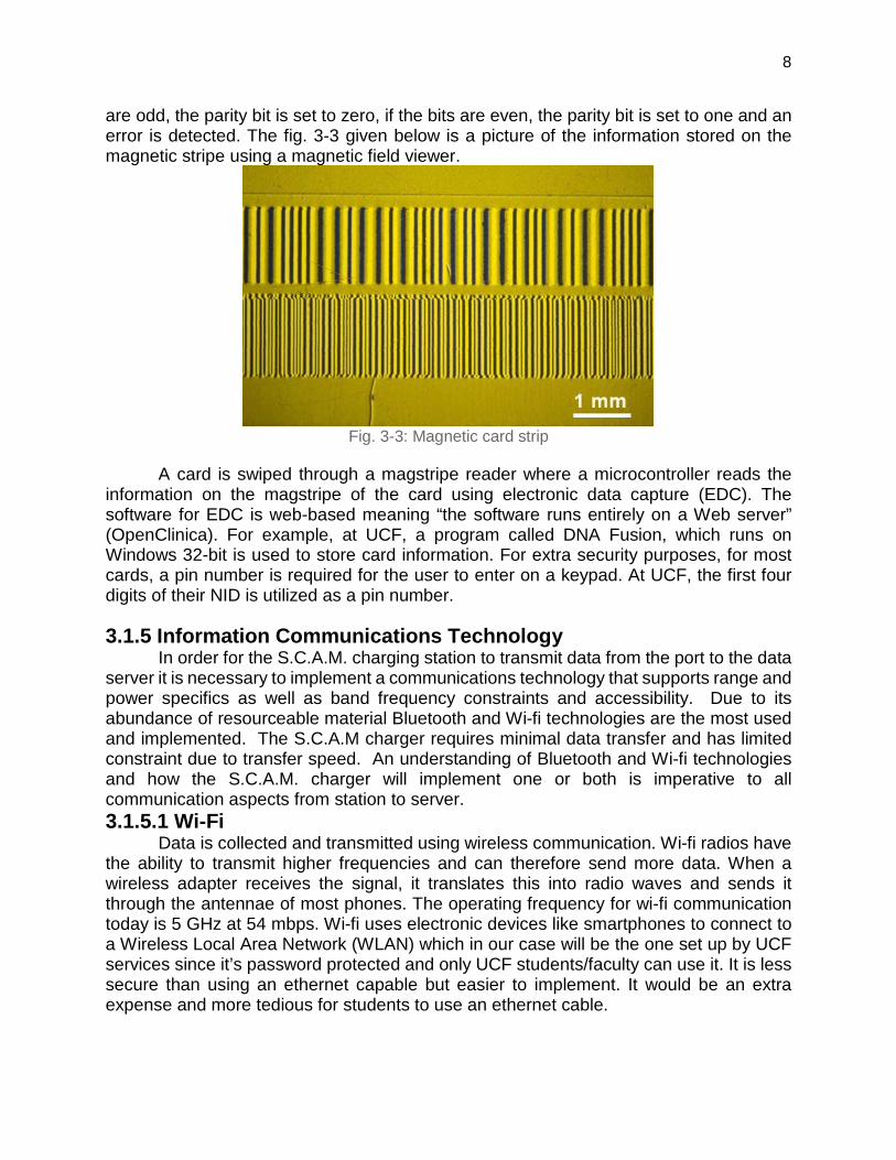
8
are odd, the parity bit is set to zero, if the bits are even, the parity bit is set to one and an error is detected. The fig. 3-3 given below is a picture of the information stored on the magnetic stripe using a magnetic field viewer.
Fig. 3-3: Magnetic card strip
A card is swiped through a magstripe reader where a microcontroller reads the information on the magstripe of the card using electronic data capture (EDC). The software for EDC is web-based meaning “the software runs entirely on a Web server” (OpenClinica). For example, at UCF, a program called DNA Fusion, which runs on Windows 32-bit is used to store card information. For extra security purposes, for most cards, a pin number is required for the user to enter on a keypad. At UCF, the first four digits of their NID is utilized as a pin number. 3.1.5 Information Communications Technology
In order for the S.C.A.M. charging station to transmit data from the port to the data server it is necessary to implement a communications technology that supports range and power specifics as well as band frequency constraints and accessibility. Due to its abundance of resourceable material Bluetooth and Wi-fi technologies are the most used and implemented. The S.C.A.M charger requires minimal data transfer and has limited constraint due to transfer speed. An understanding of Bluetooth and Wi-fi technologies and how the S.C.A.M. charger will implement one or both is imperative to all communication aspects from station to server. 3.1.5.1 Wi-Fi
Data is collected and transmitted using wireless communication. Wi-fi radios have the ability to transmit higher frequencies and can therefore send more data. When a wireless adapter receives the signal, it translates this into radio waves and sends it through the antennae of most phones. The operating frequency for wi-fi communication today is 5 GHz at 54 mbps. Wi-fi uses electronic devices like smartphones to connect to a Wireless Local Area Network (WLAN) which in our case will be the one set up by UCF services since it’s password protected and only UCF students/faculty can use it. It is less secure than using an ethernet capable but easier to implement. It would be an extra expense and more tedious for students to use an ethernet cable.

9
For the S.C.A.M. charger, a transceiver will be used to send and collect data for the users and UCF Parking services. Wi-Fi technologies require the transmission to deliver a power of at least 40 mW while complying with the spectrum mask, this means that to implement Wi-fi on the S.C.A.M charger considerably more power is needed and the chosen RF controller is required to be more durable and capable of more stress. The IEEE802.11b supports a maximum data rate of 11Mb/s with complementary code keying modulation which well exceeds the basic needs of the S.C.A.M. charging station data requirements. The tradeoff in cost and constraints on implementation were weighed closely with the application radius needs. For the S.C.A.M. charging station Android application to be fully functional spanning the entire campus Wi-Fi technologies are logical. Due to its ability to network Wi-fi allows for the S.C.A.M. charging station to transfer large data packets at a much faster rate and puts no constraints on the S.C.A.M. charging station android application features.
Commonly known as IEEE802.11a/b/g standard, it allows high-speed wireless connectivity, providing a maximum data rate of 54Mbps/s. The 11a and 11g versions are identical except for their frequency bands (5GHz and 2.4 GHz respectively). The 11b version also operates in the 2.4 GHz band but with different characteristics. The 11g and 11b standards are also known as “Wi-Fi”.
The 11a/g standard specifies a channel spacing of 20 MHz with different modulation schemes for different data rates. We note that higher data rates used denser modulation schemes, posing tougher demands on the TX and RX design. Also for rates higher than a few megabits per second, wireless systems employ OFDM so as to minimize the effect of delay spread. This standard incorporates a total of 52 subcarriers with a spacing of 0.3125 MHz. The middle sub channel and the first and last five sub channels are unused. Moreover, four of the sub carriers are occupied by BPSK-modulated “pilots” to simplify the detection in the receiver in the presence of frequency offsets and phase noise. Each OFDM symbol is 4 us long.
The TX must deliver a power of at least 40 mW (+16 dBm) while complying with the spectrum mask. Here, each point represents the power measured in a 100kHz bandwidth normalized to the overall output power. The sharp drop between 9MHz and 11MHz calls for pulse shaping in the TX baseband. In fact, pulse shaping reduces the channel bandwidth to 16.6 MHz. The carrier frequency has a tolerance of ±20 ppm. Also, the carrier leakage must remain 15 dB below the overall output power.
The receiver sensitivity in 11a/g is specified in conjunction with the data rate. The “packet error rate” must not exceed 10%, corresponding to a BER of less than 10-5.
The large difference between the sensitivities does make the receiver design difficult: the gain of the chain must reach about 82 dB in the low-rate case and be reduced to about 65 dB in the high-rate case. (As a rule of thumb, a receiver analog baseband output should be around 0 dBm).
The adjacent channel tests are carried out with the desired channel at 3 dB above the reference sensitivity and another modulated signal in the adjacent or alternate channel.
An 11a/g receiver must operate properly with a maximum input level of -30 dBm. As explained for Bluetooth such a high input amplitude saturates the receiver chain,

10
a very serious issue for the denser modulation schemes used in 11a/g. Thus, the RX gain must be programmable from about 82 dB to around 30 dB.
The IEEE802.11b supports a maximum data rate of 11Mb/s with “complementary code keying” (CCK) modulation. (CCK is a variant of QPSK). But under high signal loss conditions, the data rate is scaled down to 5.5 Mb/s, 2Mb/s or 1 Mb/s. The last two rates employ QPSK and BPSK modulation, respectively. Each channel of 11b occupies 22 MHz in the 2.4-GHz ISM band. To offer greater flexibility, 11b specifies overlapping channel frequencies. Of course, users operating in close proximity of one another avoid overlapping channels. The carrier frequency tolerance is ±25 ppm.
The 11b standard stipulates a TX output power of 100mW (+20 dBm) with the spectrum mask. Unlike the 11a/g specification, the leakage is not with respect to the overall TX output Power where each point denotes the power measured in a 100 kHz bandwidth. The low emission in adjacent channels dictates the use of pulse shaping in the TX baseband. The standard also requires that the carrier leakage be 15 dB below the peak of the spectrum.
An 11b receiver must achieve a sensitivity of -76 dBm for a “frame error rate” of 8x10⁻² and operate with input levels as high as -10 dBm. The adjacent channel can be 35 dB above the desired signal, with the latter at -70 dBm.
3.1.5.2 Bluetooth
Bluetooth establishes a communications link between two devices at a relatively low power and significantly low cost by using short-wavelength UHF radio waves in the ISM band from 2.4 to 2.485 GHz. As per the current design constraints is not imperative for data transfer speeds to be excessive Bluetooth operates at a rate of around 720kbps which is sufficient for data rates needed by the S.C.A.M. charging station. However, range is an issue with Bluetooth technology. To operate the S.C.A.M. charging station Android application a user would be required to be within a radius of no more than 30 meters. Per design objective the S.C.A.M. charging station also requires access to the UCF affiliate related data base, which requires the highest level of security. Bluetooth offers a more limited level of security as the counterpart to Wi-Fi under specific configuration considerations, while not considered to be ‘unsecure’ Wi-fi allows for multiple levels of security to be implemented where Bluetooth offers two distinctive levels. 3.1.6 Transceiver
The CC 3100 wireless network connection system is a low cost low power microcontroller that will allow the S.C.A.M. to be Wi-Fi capable. Keeping the S.C.A.M. charging station compact is important to the design and to remain within the required dimensions, it is necessary to avoid using an off board receiver transmitter. Importing the second MCU dedicated specifically for communication purposes the integrated CC3100 allows for the minimal data transfers required from the S.C.A.M. processing unit. The low power deep sleep mode allows the MCU system to not draw current while the charging system in non-operational keeping run time cost as low as possible. All files are stored in 4 KB blocks requiring a minimum of 4 KB of flash space to be available. Encrypted files with fail-safe support and optional security are twice the original size and use a minimum of 8KB. Encrypted files are counted as fail safe in terms of space. The maximum file size is 16MB. Typical Fail-safe and Non fail-safe requirements listed in table 3-3.

11
Item Typical Fail-Safe Typical NonFail-Safe
Service Pack 224KB 112KB
System and configuration files
216KB 112KB
Total 4Mb 2Mb
Recommended 8Mb 4Mb Table 3-3: Fail safe and Non-fail safe requirements
3.1.6.1 Error Vector Magnitude Error vector magnitude is a measure of how accurately a radio is transmitting symbols within its constellation. EVM is a measure of signal quality, which is a function of noise, interfering signals, nonlinear distortion and the load of the radio. It is a component of the 802.11 IEEE standard, and has become an industry standard measurement for wi-fi. The CC3100 RF transceiver has a maximum RMS output power measured at 1 dB from IEEE spectral mask. This means that the EVM of the S.C.A.M. charging station error vector has a magnitude that is 1 dB less than the average signal vector or the average energy per symbol transmitted. The constellation refers to the method of transmitting data that is used such as 16-QAM digital modulation. The antenna’s impedance presents itself as a load to the radio. If the antenna has a poor impedance match then it will have a high voltage standing wave ratio. This offers a difficult load for the radio to handle, causing a lot of power to be reflected to the radio. The radio may be jolted such that the signal quality of the radio degrades, which is measured by a higher than normal EVM. It is highly important to properly impedance match as to not raise the EVM levels out of range within the system making it difficult to transmit data. Noise, distortion, spurious signals, and phase noise all degrade EVM, and therefore EVM provides a comprehensive measure of the quality of the radio receiver or transmitter for use in digital communications. 3.1.6.2 Electromagnetic Compatibility Electromagnetic compatibility is the branch of electrical engineering concerned with the unintentional generation and reception of electromagnetic energy which may cause unwanted effects such as electromagnetic interference. EMC deals with two main issues, emissions and susceptibility. Emissions is the generation of electromagnetic energy by some source and its release into the environment. Susceptibility is the tendency of electrical equipment to malfunction or breakdown in the presence of unwanted emissions known as Radio frequency interference. To ensure the correct operation in the same electromagnetic environment use or respond to electromagnetic phenomena the S.C.A.M. charger is equipped with dual T.I manufactured RF controllers and Microcontrollers.
In the high voltage interface module the main concern for Electromagnetic interference is provided by the power source. The power generated to charge the Electric vehicle and operate components within the circuit are being directly lifted from the electrical grid and proper antenna placement should allow minimal electromagnetic

12
interference within the system. The transceiver efficiency can be affected by the frequencies generated from the power supply. The harmonics from the generated frequencies can affect the operation of the transceiver. The CC3100 RF transceiver Channel-to-channel variation is up to 2 dB. The edge channels (2413 and 2472 MHz) have reduced TX power to meet FCC emission limits. In pre regulated 1.85-V mode, maximum TX power is 0.25 to 0.75 dB lower for modulations higher than 18 OFDM. The device required an external bandpass filter to meet various emission standards, including FCC. 3.2 Hardware 3.2.1 ADC An analog-to-digital converter (ADC) converts a physical quantity like voltage and current, to a digital quantity that can be read by the microcontroller. Its main function is to sample the input of a continuous waveform and convert it to a discrete binary signal. When choosing an ADC, the bandwidth and the signal-to-noise ratio should be considered. For the S.C.A.M. charger, power measurement requires the monitoring of the current and voltage. In order for the user to get information on the amount of charge, an ADC must convert the collected data for the microcontroller to read and calculate power. There are several types of ADCs to choose from:
Pipeline ADC: It “employs a parallel structure in which each stage works on 1 to a few bits” (Maxim 5). While it is accurate, the amount of time from input to output is significantly longer than other types of ADCs.
Flash ADC: It uses a “large bank of comparators” (Maxim 5) with a flip-flop circuit at the end to store the data. An advantage of using a Flash is the speed; its sampling rate is the fastest of the ADCs. However, because of its complex circuitry, with an increase in the number of bits, there is an increase in the number of comparators making it very inconvenient.
Sigma-Delta Converter: Another name for this ADC is oversampling. Oversampling is when the input is sampled at a higher rate than the nyquist frequency. According to Maxim Integrated, “the ADC's sampling rate must be at least twice the maximum bandwidth of the signal. This maximum bandwidth is called the Nyquist frequency.” Because of the high sampling rate, an advantage of using this ADC is the high resolution. However, because of the constant sampling, it has a low speed and latency.
SAR ADC: The best option for an ADC, it uses an N-bit register to constantly sample the input. Because of the simple circuitry it’s available at a low cost. It has a sampling rate that matches the Flash ADC with low power consumption and high resolution.
For the design of the S.C.A.M. charger, a SAR ADC will be used because of the advantages of the previous ADCs. Fig. 3-4 below gives the basic architecture of the SAR ADC.

13
Fig. 3-4: SAR ADC Architecture
The input is on track/hold. A track/hold is usually made up of a switch and capacitor. When the input is on track, the switch is closed and the input continues to be sampled. When the input is on hold, the switch opens and the last input to be fed in before the switch closes stays on the capacitor. The N-bit register is initially set to 1 being its most significant bit. The value of Vin and Vdac is compared using an op-amp comparator. If Vin is less than Vdac, the register is cleared to zero. If Vin is greater than Vdac, the register remains as 1. The SAR Logic shifts the register to the right by one and starts over. The output is then a digital value made up of 1’s and 0’s. The microcontroller used for this design is the msp430f5529 which comes equipped with pins dedicated to a SAR ADC. The ADC chosen is the ADS7950 which has four channels and a 12-bit resolution. From the datasheet, the input signal is sampled using chip select input (CS) pin at falling edge and the serial clock input (SCLK) is used for conversion and data output. 3.2.2 System Voltage Regulation
As stated before, the power supply of the S.C.A.M. charger uses 120 VAC; this is considered a high power supply and will be used to power several smaller components like an MCU and a user interface module. After the power supply is converted from an AC to DC value, the voltage value must be stepped down to a voltage that’s appropriate for the other components. This concept of stepping down the voltage is called DC to DC conversion. Two ways to do this is using a voltage divider or using a voltage regulator. A voltage divider uses two registers to step down the voltage. The output voltage is dependent on the input voltage. A voltage regulator “provides a constant voltage to a load” regardless of the input voltage. This concept is extremely important for the smaller components; no matter how much the input voltage fluctuates, the amount of voltage needed for the MCU must remain the same. Therefore, a voltage regulator is used over the voltage divider in the high voltage module. When choosing a voltage regulator, there are several options to consider; an article from powerelectronics.com describes them best. The first two options are adjustable or fixed regulator. An adjustable regulator allows you to change the output voltage for different types of scenarios. In the case of the S.C.A.M. charger, changing the output

14
voltage of the MCU will not be necessary therefore a fixed regulator is the best option. Another topic to consider is output current; the output current of the voltage regulator should be close the to required current of the MCU. Finally, the output voltage of the regulator must be with the range of the required voltage. There is room for error with the most being 5%. Next, types of regulators will be discussed. Research for the types of regulators comes from the Power Management Circuits textbook Ch. 9. 3.2.2.1 Linear Regulator
This type of regulator works exclusively with DC values and only has the ability to step down the voltage. An amplifier is used in most designs to adjust the output voltage enough so that the value will stay constant regardless of the input voltage. In ideal situations, the output current of the regulator will have no affect on the output voltage. However, in practical situations, the current does have a small affect. The change in voltage divided by the change in current is the output resistance. Preferably, when choosing a regulator, the output resistance should be as low as possible. Other important parameters to consider is load and line regulation. Load regulation is the percent change of the output voltage between the circuit having no load and a full load. Ideally, the load regulation will be close to zero. However, in practical situations, adding a load will change the output voltage slightly. When picking a regulator, the load regulation value typically is around 0.8%. Line regulation is the change in output voltage divided by the change in the supply voltage; its value is used to determine how much the output voltage changes due to changes in the input. Another parameter to consider is the dropout voltage; the minimum voltage difference between input and output to maintain regulation. When choosing a regulator, having a low dropout voltage is important; it decreases the power dissipation of the regulator. A class of regulators called Linear Drop Out (LDO) are known for providing low dropout voltage values. Fig. 3-5 given below is an example of a traditional LDO regulator.
Fig. 3-5: Traditional LDO Regulator
While the linear regulator is simple to implement, there are some disadvantages.
The power efficiency for linear regulators tends to be low with the typical value being

15
below 50%. Sometimes a circuit design will require the voltage to be stepped up; another disadvantage is that the linear regulator can only step down voltage.
A specific type of regulator called a controller is another choice from the types of linear regulators. The only difference with the controller regulator is that the passive device, usually a MOSFET, is not included with the regulator. This allows the user to choose which type of passive device to use. This way the designer can decide the maximum current, power rating, and size giving the regulator more flexibility for different types of projects. The max temperature of the passive device should also be taken into account. A disadvantage is the cost; two packages must be bought now, one for the regulator and one for the passive device.
3.2.2.2 Switching Regulator This type of regulator uses the duty cycle of a pulse width modulator to keep the output voltage constant and has the ability to step up and down the voltage. Another advantage of using a switching regulator is the high power efficiency value with the typical values being above 80%. For the S.C.A.M. charger, a high power voltage supply is being used; switching regulator are able to handle higher levels of voltage than a linear regulator. Therefore, the recommended type of regulator for the S.C.AM. charger is the switching regulator. There are two types of regulators, as said before, one that steps down called the buck converter and another that steps up called the boost converter. Both types will be discussed.
Buck Converter: For this circuit, usually a transistor at the positive terminal of the input voltage is used as a switch that turns on and off based on the voltage output measured by the pulse width modulator. When the switch is on, the current across an inductor increases. It should be noted that the current across the inductor is the same value as the output current. Although there is a capacitor in parallel with the load, it’s assumed that the value is very large, therefore that current is negligible. When the switch is off, the inductor current reverses its polarity. The amount of time the switch is closed is called the duty cycle. The relationship between output voltage and input voltage is Vout = Vin * D where D is the duty cycle. The duty cycle is always between 0 and 1, and determines what the value of voltage output will be in proportion to the input voltage. Since D is between 0 and 1, the output voltage will always be lower than the input making the buck converter a step down switching regulator.
Boost Converter: For this circuit, a transistor is placed in parallel at the positive terminal of the inductor. When the switch is on, current starts to build up across the inductor. When the switch is off, or opened, that same current starts to flow across a diode to the load controlling the output voltage. Like the buck converter, the duty cycle determines the proportion of output versus input voltage. The relationship between the two is Vout = Vin/(1-D). Due to the 1-D in the denominator, the output voltage will always be higher than the input making the boost converter a step up switching regulator.
Buck-Boost Converter: A combination of the two types previously discussed, this circuit can step up and down the voltage. A two way converter can be implemented by cascading a boost converter followed by a buck converter.

16
The switching regulator has many advantages compared to the linear regulator. The only disadvantage is that the cost to buy and implement a switching regulator is higher that the linear regulator. 3.2.3 High Power Safety The required amount of voltage for the S.C.A.M. charger is 240 VAC. When dealing with high voltage power supplies, safety features must be implemented to protect some of the smaller components. For example, in the design, a voltage regulator is used to step down the voltage for the MCU that will handle power monitoring. All MCU’s have required voltages and currents that is recommended in datasheets to avoid damage. An electric vehicle also has specifications to abide by as well; the maximum amount of current that a typical EV will draw is 32 A. One way to protect a circuit is by limiting the current. A circuit breaker is used for most electric vehicle monitoring right before power it’s sent to the vehicle; it only allows a certain amount of current to go through. Once that current is exceeded, a trip will open the breaker not allowing any current to pass through. Depending on the project, there are several types of trips to pick from. A circuit breaker with a manual trip is equipped with a button that opens the circuit. This design is not ideal for the S.C.A.M. charger; if overcurrent occurs, a trip must happen immediately so as not to cause more damage to the vehicle. A circuit breaker with an overload trip is equipped with a bimetallic strip that bends to an open position whenever there is an overflow of current. This is the best option for the S.C.A.M. charger since it happens automatically. The type of circuit breaker that’s recommended for the S.C.A.M. charger is the thermal-magnetic circuit breaker; it trips immediately in the event of a short circuit and after a short delay, opens a switch in the case of a current overload. When choosing the right circuit breaker, the voltage and continuous current rating should be taken into account. It’s recommended that both these values are higher than the actually supply. For the S.C.A.M. charger when power is going from the grid to the vehicle, the voltage rating should be higher than 240 VAC but not lower and the current about 40 A. Another problem that can occur with high power supplies are ground faults. The most common one is single-line to ground faults which happens when there is a break between the electrical equipment and ground. With the current having nowhere to go, it could take a different path to ground using a person and causing serious injuries. Another type of circuit breaker called a ground-fault circuit interrupter (GFCI) can prevent this. It compares the amount of current coming in and out; when there’s a difference, a trip will stop current from flowing through. 3.2.4 EV batteries
The technology for EV batteries have been around almost as long as gasoline-powered vehicles. According to Electric Vehicle Battery Technologies, the two major batteries used by electric vehicles today are Lithium-ion (Li-ion) and nickel metal hydride (NiMH). Only recently as electric vehicles become a staple on the highways with improvements in the research and development regarding specific energy. Specific energy is the amount of energy per unit of mass; gasoline has a specific energy of 13,000 Wh/kg which is “100 times higher than the specific energy of typical Li-ion batteries” (Young 5). However, Li-ion batteries has a high electric propulsion so not as much energy

17
is needed like gasoline. “The total amount of energy stored for EV can be a quarter of what a regular ICE (internal combustion engine) powered vehicle needs for the same mileage” (Young 5). With this kind of improvement, electric vehicles are gaining and will continue to gain owners. For the S.C.A.M. charger, characteristics on car batteries and performance were researched since tracking power consumption is an important goal. Batteries are measured by their rated Ah capacity, the amount of discharge per hour from a fully charged battery. The value of the capacity varies for different batteries so an EV charger must be able to measure the amount of charge in a battery and provide the proper amount. This measurement is called the state of charge (SOC), the remaining capacity over the rated capacity. The charging method used for the S.C.A.M. charger is constant voltage. A constant value of 240 VAC will be applied to the vehicle with the amount of current decreasing to zero. Another method that some charging stations use is constant current, where the “SOC will increase linearly versus time” (Young 9). A disadvantage of this method is the SOC is difficult to measure. A combination of both methods is commonly used in charging stations as well. Next, the two types of EV batteries will be discussed in more detail.
NiMH Battery: This battery is categorized as an alkaline battery meaning it uses “potassium hydroxide as the electrolyte” (Kopera 6). Like all batteries, it has a positive and negative electrode. The positive electrode is nickel hydroxide and the negative electrode is a metal hydride. With this combination, the NiMH battery can withstand a wide range of temperatures and is compatibility with high power systems. The figure below is from the Electric Vehicle Battery Technologies and it briefly describing the charging scheme of the NiMH battery.
Fig. 3-6: NiMH Battery Charging Scheme
Li-ion Battery: The lithium ion battery is the most common EV battery used today.
It’s “positive electrode is made from chemical compound named lithium cobalt oxide or lithium iron phosphate” (Oswa 3). The amount of power loss in a Li-ion battery compared to the NiMH is significantly lower and it’s lighter weight makes it ideal when replacement is necessary. However, a disadvantage is it’s lifespan ranging from 2 to 3 years after buying a new one. The figure below is the charging scheme of a Li-ion battery from the same article.

18
Fig. 3-7: Li-ion Battery Charging Scheme
3.3 Application Software 3.3.1 Hardware to Application
One of the main motivations for making the S.C.A.M. charger was easy tracking of a vehicle’s power consumption. Because of the university’s campus wide wi-fi connectivity, the best option to implement this goal is designing a simple application for a smartphone that allows the user to track the amount of charge there vehicle has. An application programming interface (API) is needed for the hardware of the electric vehicle monitor to communicate with the phone app. Using an API will allow data and information to be shared and exchanged with other services; another motivation for the S.C.A.M. charger was to exchange power consumption information with UCF parking services, therefore an API is an easy and useful way to make this exchange. According to the API basics website, an API should “work well with any common programming language.” A common format for APIs is REST, REpresentational State Transfer, used for the world wide web. There is no standard for how to implement an API but the usual practice is to allow the API to communicate with an additional API that a mobile application will use. The API should be easy and accessible to everyone while the additional API is more specific towards the phone. When the data is being returned, instead of it returning in HTML, two common formats can be used: XML and JSON. Both choices use spreadsheets that are easily read both programmers and non-programmers, however using REST with JSON has become the common practice among developers. To make sure the right people have access to the API, security standards must be put in place. The Basic Auth and OAuth are two standards that require a username and password for access and protects that information from other parties. For further protection, the designed code should be able to handle emergency errors like the UCF servers going down.

19
3.4 Power Systems
A key component to implementing the S.C.A.M. charging system is determining where power is going to be extracted. To develop a level II charging station it is necessary to have a reliable 240 volt energy system available. The most practical options are to use the Electrical Grid, a Photovoltaic system, or some hybrid of both. To determine which power system is the most appropriate for a senior design project, it is necessary to evaluate the pros and cons of each system, as well as cost and implementation. 3.4.1 Photovoltaic System
A photovoltaic system, commonly referred to as Solar power, is a means of producing usable energy by means of sunlight. Photovoltaics is a process of converting solar energy into DC current using semi-conducting materials. The system then takes that DC current and converts it to usable AC current that is stored in solar cells. For the S.C.A.M. system a photovoltaic system can be quite useful in that the solar energy is converted directly into DC current, which is what Electric Vehicles use to charge. However to use the DC current it would require that an already constructed solar panel system be dismantled and altered in some way, or that a solar system was developed specifically for powering the S.C.A.M. system that circumnavigated storing AC current. With a group size of 3 and a time limit of two semesters, it is impractical to develop a system specifically for the S.C.A.M. charging station as it would put a huge strain on time and resources. As well as time constraints, a budget dictated by the S.C.A.M. charging station sponsorships do not warrant the cost increase to use an already implemented solar system as the S.C.A.M. power supply. 3.4.2 Electrical Grid
The electrical grid is an interconnected network for delivering electricity from suppliers to consumers. Apart from a few dedicated areas on UCF campus where Solar power is used, the electrical grid is the most used source of electrical use. Outlets that dictate voltage are located in and on every building around campus. To classify the S.C.A.M. charging station as level II appropriate, 240 volts is required. Using the electrical grid it is possible to use a transformer to upconvert the 120 voltage output to usable 240 volts needed. However, much like the cost issues associated with a photovoltaic system, a transformer that would output the necessary current needed to charge a vehicle would strain the project budget significantly. Therefore, to implement a level II charging station from the electrical grid it is necessary to secure a 240 volt outlet with at least a 40 amp capable circuit. With the proper permissions securing a high voltage outlet would decrease production cost and production time of the S.C.A.M. charging system by half. Fortunately 240 volt circuits are common enough that no extra circuit work will be required. 3.5 Expansion The process of designing the S.C.A.M charging station requires decision making choices to troubleshoot current and future problems. As the construction phase of assembling the the S.C.A.M station it is important to research possible expansion and or alternate components that may be more time efficient to implement. A quick overview of

20
components currently in consideration for operations essential to the S.C.A.M system are explored and researched. 3.5.1 PCI Express Communication is an essential part of any integrated circuit whether communicating to components embedded in the system or transferring data over a server. Considering how data is going to be transmitted and received is important. Due to time constraints the most standard approach to transmitting data is to select an industry MCU Transceiver. PCIs are Multi-Gigabit Transceivers capable of operating at serial bit rates above 1 Gigabit/second. They are used for data communication because they can run over longer distances, use fewer wires, and are generally lower in cost than parallel interfaces with equivalent data throughput.
The primary function of the Multi-Gigabit transceiver is to transmit parallel data as stream of serial bits and convert the serial bits it receives to parallel data. PCI Express uses Electrical idle signals to indicate when endpoints should go in and out of low power modes, this requires Multi-Gigabit Transceiver circuitry capable of generating and detecting Electrical idle/OOB signals on the serial lines. Time constraints of the senior design project indicate that implementing a PCI Express for the initial communication needs is unlikely. However, MGTs can be added to a system already in possession of a communication protocol to increase stability and throughput. Adding a PCI to the system can terminate impedance matching at high line rates the wires used to carry serial data have many of the properties of transmission lines. The signals on the line can be distorted if the impedance of the MGT at the transmitter and receiver does not match the impedance of the line.
A good MGT is typically designed to match the impedance of the wires that connect them as closely as possible commonly 100Ω which will help to eliminate noise transferred into the system. Another reason to consider an addition of a PCI is as a storage device. The S.C.A.M charging station requires a relatively small database of user information and code. PCI Express protocol can be used as data interface to flash memory devices, such as memory cards and solid-state drives. This means that a PCI card can be selected and inserted into the charging station for access to data on board. The PCI would then speak with the already chosen CC3100 transceiver solution and be internet ready to transmit data over a server. 3.5.2 Raspberry Pi 2 It has been determined that I/O spacing may become an issue dealing with communication protocols and hardwiring the integrated circuit to communicate with itself. To ensure that components don’t interfere with each other the solution becomes to introduce another component. Addition of a third MCU specific to it’s own board will allow for the circuit to be spread out in spacing. This allows for less interference of signals and makes it easier to physically build. The Raspberry Pi 2 would require a separate path for power as it takes a different operational voltage then the MSP430 F5529. Currently external components are being controlled by the Raspberry Pi 2 including the Keypad and swipe card interface. This was chosen because the Raspberry Pi 2 has a very direct USB interfacing system that makes it easy to operate and power the external components.

21
4. Standards According to the EV Charging Technology Analyses and Standards document, an
EV charging station must abide by the codes established by the National Electric Code (NEC) and the Occupational Safety and Health Administration (OSHA) as well as standards approved by the Society of Automotive Engineers (SAE). Specifically, Article 625 of the NEC deals with the electrical wiring and installation of EV charging stations to electric vehicles while the standard SAE J1772 focuses on the communications between the station and the vehicle. The standards for EV charging is constantly changing and always developing. The International Electrotechnical Commission (IEC) has developed a set of standards that involve EV charging and EV charging couplers. 4.1 Power Supply
The power supply for the EV charging station will be provided by the UCF Parking Garages. The typical voltage rating of a power supply at UCF is 120 VAC. This value complies with the NEC article 625 that states, the “ac nominal system voltages used to supply the equipment will be 120 120/240, 208Y/120, 240, 480Y/277, 480, 600Y/347, or 600 volts” (NEC 973). 4.2 EV Charging Station
The type of charging chosen for this design will be AC level 2 charging. According to the standard SAE J1772, AC level 2 charging must provide a voltage between 208-240, a maximum current of 32 A, and a branch circuit breaker rating of 40 A. The NEC article 625 lists explains in detail every code Electric Vehicle Supply Equipment (EVSE) must abide by. For the codes concerning the cables, in this design, the SAE J1772 cable will be used which already complies with the NEC; however, the cable must be a maximum of 25 feet long. As for the main supply equipment, the codes are as followed when it comes to installation:
Any non-portable supply equipment must be attached to the wall, floor, or ceiling with no live parts exposed.
The EVSE should provide an interlock that “de-energizes the electric vehicle (EV) connector and cable whenever the connector uncouples from the EV” (NEC 974). Also, a loss of pilot or communications circuit should lock out the power.
An automatic de-energization of the cable conductors and EV connector upon exposure to strain that results in either a cable rupture, separation of the cable, or exposure of live parts.
On the EVSE, there should be markers stating “For Use With Electric Vehicles” and either “Ventilation Not Required” or “Ventilation Required.”
For personnel protection, components can be added to reduce the risk of electric shock such as: insulation; grounding, insulation, and leakage current monitors.
Unless otherwise specified, an EVSE shall be stored or located at a height of no less than 600 mm (24 in.) and no more than 1.2 m (4 ft).

22
4.3 Security
One of the goals for this design was to allow only UCF students and faculty to use the EVSE for their vehicles. This will be achieved using UCF NID, a form of identification that everyone associated with UCF has. Listed below are standards that the security aspect must abide by:
An interface that allows students/faculty to type in their NID. For our purposes a keypad to type in NID will be used.
Correct mapping to the UCF servers that confirms a person’s NID. An application only UCF students/faculty can use to track the amount of charge for
their vehicle. 4.4 Communication Protocols
There are two types of communication involved in this design; vehicle to station and station to network. For connection from vehicle to station, a circuit must be designed that meets the SAE J1772 standards. According to the SAE J1772, two pins, the pilot and proximity pins, are required. The pilot pin must communicate with the vehicle to determine whether the cable is connected or not and ready to be energized. The J1772 pilot pin must be a 1 kHz square wave with an amplitude of 12 V. The proximity pin is used as a switch to turn on and off the current flow. For the connection from station to network, inside the EVSE, there should be power monitoring circuit, that tracks charge and sends this information to an application for the user and Parking Services. The wireless communications provided by UCF will be used which satisfy any communication protocols. There was no standard set for what type of phone the application would be for. It was collectively agreed that an android application would be designed and developed. 4.4.1 USB Universal Serial Bus is an industry standard that defines the cables, connectors and communications protocols used in a bus for connection, communication, and power supply between computers and electronic devices. It was designed to standardize the connection of the computer peripherals. The MSP430 F5529 utilizes multiple USB ports allowing the integrated circuit options to connect the microcontroller to components and devices increasing the features of the S.C.A.M. charging station without having to overload the MCU or the PCB. A keypad can be chosen to implement a secure system of identification from the microcontroller to the user via a single rerouting of power from the power monitoring system. 4.4.2 SPI Serial Peripheral Interface is a bus of synchronous serial communication interface specifications used for short distance communication. SPI is used to send data between microcontrollers and small peripherals such as shift registers, sensors, and SD cards. SPI devices communicate in full duplex mode using a master-slave architecture with a single master. The master device originates the frame for reading and writing. Multiple slave devices are supported through selection with individual slave select lines. Although SPI may be accurately described as a synchronous serial interface it differs from the

23
synchronous Serial Interface Protocol, which is also a four-wire synchronous serial communication protocol, but employs differential signaling and provides only a single simplex communication channel. The S.C.A.M. charging station utilizes the SPI communication protocols to allow the RF board to communicate with the MCU as well as allowing other integrated circuits to create a symbiotic system. The CC3100 RC system has 14 shift registers available allowing the integrated circuit to save pins on the microcontroller. This allows the S.C.A.M. charger to allot extra pins for switch operations where it would have needed the pins for inter circuit communications. 4.4.2 UART UART translates data between parallel and serial forms via a computer hardware device. Differential signaling is handled by a driver circuit external to the UART. In synchronous mode it is required that the sender and receiver share a clock with one another, or that the sender provide some other timing signal to the receiver for the next bi of the data. In asynchronous mode the sender and receiver must agree on timing parameters in advance. To do this extra bits must be added to each word which are then used to synchronize the sending and receiving units. When a word is given to the UART for asynchronous transmissions, a start bit is added to the beginning of each word that is to be transmitted.
A UART is an added component to the integrated circuit used for serial communication over a computer or peripheral device serial port. More commonly now microcontrollers are being manufactured with integrated UART capabilities. The MSP430 F5529 chosen for the S.C.A.M. charging station is UART accessible allowing transmitting and receiving data through pins 3.3 and 3.4 respectively. This allows the RF board to communicate with the server and then inpart the RF board communicates with the microcontroller. 4.4.4 I2C Inter-integrated circuit is a multi-slave serial computer bus typically used for attaching lower-speed peripheral ICs to processors and microcontrollers. The Bus physically consists of 2 active wires and a ground connection. I2C uses a bidirectional two wire design that allows for simplicity in the system. The two lines are the Serial data line and the serial clock line pulled up with resistors. Typical voltages used are +5V or +3.3V although systems with other voltages are permitted. The I2C reference design has a 7-b or a 10-bit address space. Protocol overheads include a slave address and perhaps a register address and perhaps a register address within the slave device as well as per-byte ACK/NACK bits. Thus the actual transfer rate of the user data is lower than those peak bit rates alone would imply. In most systems the microcontroller is the master and the external peripheral devices are the slaves. The MSP430 F5529 is fully capable of using I2c for communication purposes but has yet to include a feature where I2C is necessary.

24
4.5 Relevant Standards Building the S.C.A.M charging station requires a set of standards and rules that must be complied with to operate the system for public use. A list of standards that directly apply to the S.C.A.M charging station are listed below with detailed description from governing bodies associated with each standard accordingly.
IEC 62196 - An international standard for set of electrical connectors and charging modes for electric vehicles and is maintained by the international Electrotechnical Commission. The standard is based on IEC 61851 which specifies mechanisms such that, first, power is not supplied unless a vehicle is connected and, second, the vehicle is immobilized while still connected.
IEC 62196-1 - Is applicable to plugs, socket-outlets, connectors, inlets and cable assemblies for electric vehicles, intended for use in conductive charging systems which incorporate control means, with a rated operating voltage not exceeding 690 V AC 50-60 Hz at a rated current not exceeding 250 A; 600DC at a rated current not exceeding 400A.
IEEE 802.11 - A set of media access control and physical layer specifications for implementing wireless local area network computer communication in the 900 MHz and 2.4, 3.6, and 60 GHz frequency bands. They are created and maintained by the Institute of Electrical and Electronics Engineers LAN/MAN standards Committee. The base version of the standard was released in 1997, and has had subsequent amendments. The standard and amendments provide the basis for wireless network products using the Wi-Fi brand. While each amendment is officially revoked when it is incorporated in the latest version of the standard, the corporate world tends to market to the revisions because they concisely denote capabilities of their products. As a result, in the marketplace, each revision tends to become its own standard.
IEEE 802.11i- 2004 - An amendment to the original IEEE 802.11, implemented as Wi-fi Protected Access II. the draft standard was ratified on 24 June 2004. The standard specifies security mechanisms for wireless networks, replacing the short Authentication and privacy clause of the original standard with a detailed Security incorporated into the published IEEE 802.11-2007 standard.
UL 94 - The Standard for Safety of Flammability of Plastic Materials for Parts n Devices and Appliances testing is a plastics flammability standard released by Underwriters Laboratories of the USA. The standard classifies plastics according to how they burn in various orientations and thicknesses. From lowest (least flame-retardant) to highest (most flame-retardant).
IEEE 1149.1 - The Joint test Action Group (JTAG) is an electronics industry association formed in 1985 for developing a method of verifying designs and testing printed circuit boards after manufacture. In 1990 the institute of Electrical and Electronics Engineers codified the results of the effort in IEEE Standard 1149.1- 1990, entitled Standard Test Access Port and Boundary-Scan Architecture

25
5. Project Description 5.1 Project Equipment 5.1.1 Overall Description
The primary goal of the S.C.A.M. station is to provide a safe, reliable and secure place for UCF students to charge their vehicles and know that at any given time it is possible to monitor the state of their vehicle in the palm of their hand. In order to implement such charging capabilities, an ordinary electric vehicle charging unit must be turned into a “smart” device. Currently all charging stations that supply Level 1 or Level 2 charging simply pass power while monitoring for cost purposes only. This “smart” device must be able to maintain itself, monitor power, store information in a database, provide means of communication between a network to provide data for an app with current charging status, be able to compute various electrical quantities and give information about the state of the physical device itself for safe operation.
The S.C.A.M. station contains a “smart” capabilities concept by using several key functionalities. Below is a block diagram of S.C.A.M. implementation.
Block Diagram 5-1: SCAM System Overview
Labeled in block diagram 5-1, the S.C.A.M. system operates by using five major components. Although the system itself does not include the grid/power outlet or the electric vehicle the system will directly connect to these items as this directly relates to system functionality. Here’s how S.C.A.M system works, power is provided through the grid or a power outlet. This power will be used to charge the vehicle as well to supply power to the entire system. As mentioned before, the station shall provide Level two charging which means that the car will receive anywhere from 208 to 240 VAC and up to a max current of 80A which corresponds to a 20 kW per hour. The EVSE will pass power straight through to the car to be charged. At the same time, the system will measure the power it’s provided to the car to eventually be reported to the user and displayed on the station.

26
In order to provide any information to the user a wireless communication link must be established. This link is established by using the wireless transceiver interface labeled in block diagram 5-1. The wireless transceiver interface will serve as the antenna and the key to making all the protocols and layers necessary to connect hardware functionality to network functionality. One important feature of the transceiver is reduce error-detection issues between layer and protocol implementation. The board layout and software implementation shall be done such that to minimize error detection; this topic is discussed more later on. By minimizing the error vector magnitude and constellation error used for wireless communication, the S.C.A.M. system will provide reliable communication between the station and network link. With a secure RF link established to the network the S.C.A.M. system shall provide data to the network communicated to a S.C.A.M. station app. The station app will contain the same information that one can get at the physical station but now one can access the station wirelessly anywhere on campus. The user will have control as to what information they want to see such as current power supplied, time of charging, how charged their vehicle is, is there are any issues developing in the station, internal temperature and have real time control over the station. The user will be able stop and restart charging at a tap of a touchscreen.
Overall the S.C.A.M. system will interact with the main grid, the electric vehicle and communicate to a network in real-time so that the user can have full control and full security over their vehicle and the charging station. A more detailed look can be viewed below in block diagram 5-2.
Block Diagram 5-2: Detailed System Overview

27
5.1.2 Installation Hardware
As mentioned before the costs on installation and software maintenance are what drives up the cost of current charging stations. In order to make this more readily available for mass production and for larger institutions (such as UCF) to able to purchase charging stations in bundles the “smart” device must be lightweight, easy to install, reduced in size and provide an easy to use atmosphere for the customer. Below in figure 5-1 is a model of the size and shape that the S.C.A.M. system will be designed to.
Fig. 5-1: Model Monitor System
Picture from Youtube “Electric Charger Home Installation by Jim Pyle”
There are several key features that the S.C.A.M. system will incorporate based off of the design in figure 5-1. The first feature is the ease of installation. The current charging infrastructure implemented at UCF using solar energy requires normal installation methods which include but are not limited to mounting space brackets, flushing the appropriate bolts onto brackets, apply station onto brackets, secure base, and attach cord to station to then do all the mounting steps. The S.C.A.M. design will only require mounting which will be as simple as placing the station onto a hook to hang much like a painting in a home or for place on a hook from a stand (which will require installment itself). Although at first this may seem insignificant, the process of installation can be time consuming, costly to the consumer and eliminates the amount of mechanical parts to order per installation.
5.1.3 MCU 5.1.3.1 MCU Selection
As shown in block diagram 5-2 the microcontroller which is what is labeled “Mixed signal Processor” interfaces between the high power hardware and the wireless transceiver interface. The main role of the MCU is to behave as the “brain” of the system by monitoring various quantities and making sure the system is doing what it’s supposed

28
to. The S.C.A.M. system will use MSP4305529 as the brain of the system. Figure 5-2 below shows what the microcontroller looks like. The MSP430 is a family of low power microcontrollers designed by Texas Instruments. This family of microcontrollers offers some of the lowest power consumption capabilities found in industry. This is attractive because the microcontroller can be in a low-power mode while still being able to perform a variety of functions and provide a signal for synchronization purposes (such as a clock signal or PWM). When an event occurs, the microcontroller can wake up temporarily, execute the demanded task then re-enter a low-power mode without much delay and consuming that much power. Using a processing unit of the MSP430 family ensures that the physical size of the CPU and the size of the instruction sets are small. It is composed of a MSP (Mixed-Signal Processor) as the CPU and contains modern high-speed peripherals with I2C, SPI, UART and USB interfaces which are found on most electronics. The variety of peripherals allows for flexibility in the design. It uses a RISC architecture meaning that commands are typically executed with minimal cycles and word lengths of control commands are kept to a minimum. Small or reduced set architectures ensure for simpler programming commands which allows for easier debugging. The remaining features for choosing MSP4305529 specifically are discussed in the subsequent sections.

29
Fig.5-2: MSP4305529 MCU
5.1.3.2 MSP4305529 Features This specific microcontroller family has unique features that made this an attractive
selection for the S.C.A.M. design team. First, some of the general features are that integrated into the device is a USB and PHY parts the support USB 2.0 which is the newer USB standard as of 2000. The device has four 16-bit timers that are capable of multiple capture/compare options, they have an ability to output PWM signals, and as all basic timers provide interval timing. A feature of the MSP4305xxx family is that Timer_B is used as opposed to Timer_A as used in previous families. Timer_B is two additional features that Timer_A, first is an incorporated second clock divider to allow for more flexibility on clock speeds, second is that for vector interrupt addresses the overflow vector is moved from 0x0A to 0x0E. The consequence of this is if multiple interrupts occurred at the same time, timer overflow vector would take the least priority. Below in figure 5-3 shows hardware used in a Timer_B block.
Fig. 5-3: One Timer_B cell from MSP430 Users Guide
Notice the added feature of the IDEX control signal allowing for wider variety of clock signal frequencies after the ID control signal block. The advantages of this extra control being added to this timer module is that accurate clocks and be used for slower tracking applications if both accuracy and low frequency modes are desired. More detail on use of MSP4305529 will be discussed later on.
Other essential features of the microcontroller are:
An embedded 16 channel 12-bit SAR analog-to-digital converter for accurate and quick conversion rates
Hardware multiplier to allow for digital signal processing of possible digital filtering Direct access memory capabilities of transferring data from ADC conversion
memory to RAM A real-time clock module with alarm options. This gives an option for easy
implementation for events that involve time stamping.

30
Two universal serial communication interfaces. For each USCI (universal serial communication interface), options for SPI, I2C and UART are available.
Internal Temperature sensor embedded into the ADC reference voltage source Capabilities of producing standard pulse modulated waveforms for Infrared
imaging applications that satisfy IrDA standards. The S.C.A.M. system will take advantage of all these unique features except for infrared image processing although design in the future may include heat image applications for better analysis and performance of electric vehicle charging. For now this feature will be put off until a later time.
5.1.3.3 MSP4305529 Low-Power Modes
As all MSP430’s and typical for microcontrollers in general, the device comes with predefined low-operating modes. Since the low-power modes for this particular device are only unique in one instance (Low-Power Mode 4.5), a summary of all the modes are listed below in table 5-1. As this will be needed in order to discuss hardware implementation. An “x” is marked if that particular feature is disabled during its respective low-power mode.
Low- Power Mode
CPU ACLK (Auxiliary Clock)
SMCLK (Sub-Master Clock)
MCLK (Master Clock)
FLL loop (Frequency Locked Loop)
DCOCLK (Digitally Controlled Oscillator)
DCO DC Generator
LPM0 X X LPM1 X X X LPM2 X X X X LPM3 X X X X X LPM4* X X X X X X LPM4.5** X X X X X X
Table 5-1: Low-Power Modes
A quick look needs to be taken in Low-Power mode 4 and 4.5. During Low-Power mode 4, despite the Master clock and auxiliary clock being disabled there’s still complete data retention allowing for flash memory storage with only one clock source running in the device. Low-Power mode 4.5 disables an internal voltage regulator (Vref), no data is saved in RAM and requires an interrupt to go through a reset (active low) non-makeable interrupt. Now that the features of the MSP4305529 and low-power modes have been discussed, the remaining sections will touch on how the MCU will be utilized in the S.C.A.M system.

31
5.1.3.4 Mixed-Signal Processor Monitoring
From the system point of view the microcontroller has three main roles. First, the MCU shall monitor various quantities to keep track and ensure the system is behaving as it is designed to. Second, the MCU is responsible for data transfer between the user module interface and the transceiver wireless interface. The main idea is to keep information synchronized between what the user will see on the screen vs. what the user will see on the S.C.A.M system app. Last major functionality is that the mixed-signal processor shall perform several signal processing calculations. The two most important signal processing calculations will be any FIR/IIR or wave digital filtering for cleaner input from measuring power and other frequency dependent quantities and mathematical calculations of power levels. A quick note on digital filters, one can mimic an analog filter digitally by first producing and IIR filter, if this filter is implemented as a recursive function to make the algorithm a more organized closed form expression, it can be turned into a FIR filter. Then if one tries to also model or mimic impedances into a discrete-time system it is often referred to as “wave digital filtering”. Therefore to avoid confusion throughout the paper, any filters implemented digital will be referred to as wave digital filter unless noted otherwise.
The majority of the “monitoring” functions that the S.C.A.M system will perform will be read through inputs to the 12-bit SAR ADC embedded within the device. Below in Table 5-2 on the next page is a list of signals of what is being monitored with its associated pin and a brief description.

32
Measurement Signal Name Port/Pin location Description PWM loop back A?_PWM_LB P6.4 PWM shall be
produced for vehicle pilot pin, this is to measure what is actually being produced as opposed to what is being commanded
Input current measurement
A?_Vi P6.5 This signal is reserved for measurement input current to the system so that the MCU can power supplied to Electric Vehicle
Input Voltage measurement
A?_Vv P6.6 This signal is reserved for measurement of input voltage to the system so that the MCU can power supplied to Electric Vehicle
Power Monitoring
Circuit Temperature
A?_Vpmt P7.0 In order to ensure the power monitoring circuit is not overheating nor the surrounding air, this shall be the temperature sensor output.
Table 5-2: Analog to Digital Converter Input Signals
Measurement Signal Name Port/Pin location Description High Voltage
Cable Interface A?_VciT P7.1 In order to ensure
the High Voltage

33
Module Temperature
Cable interface components is not overheating nor the surrounding air, this shall be the temperature sensor output.
Proximity A?_Vprox P7.2 This for smooth start up for when user inputs charging cable
Vref_+ A8_VREF+ P5.0 Either output of reference voltage if selected internally or external voltage reference input
Vref_- A9_VREF- P5.1 Same as P5.0 except for lower limit voltage for ADC conversion
Signal for Testing
Purposes
A0_BIT P6.0 This pin is reserved to for Build it testing (BIT) to measure ADC timing parameters.
Table 5-3: Analog to Digital Converter Input Signals (continued)
For ADC built in test, all signals except BIT will be tested by voltage magnitude whereas the remaining BIT signal is used specifically for measuring ADC timing parameters. Below in figure 5-4 is the timing diagrams for the 12-bit ADC More information on this topic will be discussed in the testing section, along with operating and testing limit requirements.

34
Fig. 5-4: Timing Diagram for ADC in Pulse Mode from User’s Guide
5.1.3.5 MCU Software Implementation Overview
The overall code for the MCU can be broken down into three parts. First MCU needs to be initialized, which will include initialization of all the modules, peripheral, clocks, ADC...etc. The main code stage which organizes the order of implementation of when the code will execute certain commands and coding the interrupt service routines. Additional software provided with the MSP F5529 microcontroller are the General MSP430 resources that are supported by several software tools to help get started programming the MCU. A USB developer’s package for the MSP430 is a software package containing all source code and sample applications required for developing a USB-Based project. Currently the S.C.A.M charging station will utilize a keypad swiper that will need to use the USB port for communication to the MCU. The package includes code examples n C and assembly. These Code examples are available for each integrated peripheral inside the microcontroller, including timers, ADC, and serial communication. TI-TROS for MSP430 is a software program that reduces development time by eliminating the need to create basic system software functions from scratch. TI-TROS is intended to operate with minimal memory footprint as it assist in debugging complex system-level problems.
5.1.3.5.1 Pin Configuration During Power on and initialization phase there are various modules that need to
be configured and initialized. The first module that will be initialized are the port pins. Configuring the port pins first allows initialization of crystal functionality since the switch functions are determined on how the user programs the MCU. Also, configuring the ports first allows for the unused pins to be dealt with. Typical recommendation for handling unused pins is that the non-connected pins be set as outputs and designed to be physically non-connected during PCB layout design. Pins that are set as inputs but are not connected during low power mode have the risk of collecting extra switching currents

35
which can cause unwanted effects. Lastly an additional feature on this MSP4305xxx family is that a drive strength for each pin is selected between reduced strength and full strength. Then with the specified strength the pins can be configured as input, input with pulldown resistor, input with pullup resistor and output.
5.1.3.5.2 Power Management Module Configuration The next module that needs to be configured is the Power Management Module
or noted as PMM on the device. The main function of the PMM module is to lower the CPU voltage which ultimately lowers power dissipation during operation. This is also the fundamental idea behind the direct access memory, where memory transfer can occur without CPU intervention since the CPU is the unit that can potentially be a big factor in power dissipation. The PMM has a Low-voltage dropout regulator this is programmable. Default setting is 1.35V which allows the CPU to operate up to 12MHz but for the CPU to operate at any higher frequency the dropout voltage must also be selected to a higher voltage.
5.1.3.5.3 Timer-B Configuration Refer to section 5.2.1.1 for Timer_B details however the module has same
capabilities as Timer_A module presented in EEL 4742C Embedded systems course at UCF of the MSP430 except that frequency range capabilities have a wider range of selection. Timer_B handles all timing events not related to calendar timing by the devices capture and compare modes.
5.1.3.5.4 ADC Configuration The analog to digital converter has several settings that need to be selected. The
12-bit ADC has an option of representing data in 8-bit, 10-bit or 12-bit resolution. After the amount of bits are determined the ADC12 module can either represent the data as unsigned binary or 2’s complement format. The sampling rate of the ADC12 can also be selected between 200 ksps or 50ksps. In order for proper ADC conversion a reference voltage, internal or external must be selected. Also for temporary storing, a reference buffer can be selected to remain on continuous mode or only during sample and convert operations. Although designs can change more about specifics of configuration will be discussed in section six.
5.1.3.5.5 Flash Configuration The flash module uses an oscillator dedicated to this module only and is set up
automatically. With this there is a marginal read as an option, banks of memory can be erased simultaneously as a program is executing. For more complex operations long word and long word block write is supported. Depending on prototyping between initial phase and senior design two will determine how this module will be handled for final product development.
Initial Device Power On
Port, Peripherial and I/O initialization

36
Flow diagram 5-1: Flash Configuration 5.1.3.6 MSP Clock Functions A crystal oscillator is an electronic oscillator circuit that uses the mechanical resonance of a vibrating crystal of piezoelectric material to create an electrical signal with a precise frequency. Due to real time clock applications needed to be performed by the S.C.A.M charging station frequency matching is paramount within the integrated circuit. This is important because microcontrollers use crystal oscillators to regulate exterior timing issues. The MSP430 F5529 has multiple clock sources for different operations. The MSP F5529 is equipped with a 12 Khz Internal Very-Low-Power Low Frequency Oscillator (VLO) which does not need an external crystal. A VLOCLK can be selected by LFXT1SX=10 when XTS=0. And the LFXT1 crystal oscillators are disabled when VLO is selected. The LFXT1 oscillator supports 32KHz external crystal in LF mode where capacitance can be selected. The LFXT1 also supports high speed crystal in HF mode at a capacitance setting that can be selected. Via the user manual the LFXT1 supports use of external clock and can be disabled if it is not sourcing SMCLK or MCLK by setting OSCOFF. The MSP F 5529 is also equipped with the XT1/2 oscillators the XT2 sources the XT2CLK, this clock characteristic is similar to LFXT1 in HF mode. Lastly the MSP F5529 is integrated with a Digitally Controlled Oscillator DCOCLK can be disabled when not sourcing SMCLK or MCLK by setting SCG0. A quartz crystal can be modeled as an electrical network with a low-impedance and a high impedance resonance points spaced closely together. Adding capacitance across a crystal causes the resonance frequency to decrease. Adding inductance across a crystal causes the resonance frequency to increase. This is how the frequency at which a crystal oscillates can be measured. The crystal oscillator circuit sustains oscillation by taking a voltage signal from the quartz resonator and feeding it back to the resonator. The rate of expansion and contraction of the quartz is the resonant frequency. The size of the crystal determines the resonant frequency. The oscillating crystals used in the MSP F5529 meet all constraint limitations the S.C.A.M charging station requires for timing. The frequency of oscillation for a
Write Main Body of Code and ISR. Enter Low
Power Mode
Are any flags
raised?

37
standard watch crystal for use with the MSP430 is 32.768 kHz. The actual frequency varies within the system due to external variables. The LFXT1 is the oscillator that is the most paramount to the integrated circuitry for the S.C.A.M charging station and the frequency timing is important to ensure all safety procedures are upheld to maximum compliance. It has an equivalent circuitry highlighted in figure 5.5.
Figure 5.5: Oscillator from MSP430 LFXT1 Oscillator Accuracy report
The circuit only represents the contributing factors to the loading of the crystal
affecting oscillation frequency and is not intended to represent the actual LFXT1 oscillator circuitry. The internal capacitance has been disabled and is assumed to be provided externally to the crystal a recommended configuration when frequency accuracy is critical like the accuracy needed in the S.C.A.M charging station circuitry. The calculated tolerances for the frequency of a 32.768 kHz watch crystal can be calculated by measuring the capacitance stray values and the crystal temperature shift as well. The capacitance shift is specific for each capacitor in the equivalent circuit and can be calculated using the tables listed in the data sheet. Tables 5-4 through 5-7 are the values and tolerances for the concurrent capacitive levels.
Table 5-4: Upper Tolerance Calculations for Internal Elements (6 pF crystal) from
MSP430LFXT1 report sheet

38
Table 5-5: Lower Tolerance Calculations for Internal Elements (6 pF crystal) from
MSP430LFXT1 report sheet.
Table 5-6a
Table 5-6b
Tables 5-6a/b: Upper Tolerance Calculations for Internal Elements (12.5 pF crystal) from MSP430LFXT1 report sheet
Table 5-7: Lower Tolerance Calculations for Internal Elements (12.5 pF crystal) from
MSP430LFXT1 report sheet
The theoretical tolerances of the MSP430 internal elements is approximately a 2.5 ppm deviation in either direction. High temperature case scenarios were considered to land accuracy of calculated numbers within a range of 10% deviation plus or minus. For the 12.5 pF crystal a maximum tolerance of 0.8 ppm deviation plus or minus is calculated.

39
The error tolerance is sizably smaller than that for the 6 pF crystal and offers more stability to the system. 5.1.3.7 SPI MCU to RC System The MSP430 F5529 is equipped with a Universal Serial communication interface that supports serial communications. With the MSP430 capable of communications both with SPI and I2C it was determined that SPI communication interface would be used rather than I2C due to a few key tradeoffs. I2C is more complex to set-up where SPI is relatively easy to set-up.
Due to time constraints it is vital to chose the most time sensitive protocols that do not inflate the budget and provide similar performance guidelines. One tradeoff SPI loses to I2C is the need to use more I/O’s, however, the design constraints on the S.C.A.M charging station do not require extensive I/O ports and therefore using all the pins on the MSP430 F5529 are not detrimental to project completion. The large spacing on the MCU board allows for connector space and less need for additional busses so SPI communication is sufficient for the S.C.A.M charger. In Synchronous mode, the USCI connects the device to an external system via three or four pins. To determine how many pins are needed it is necessary to view the data sheet of the device you wish to communicate with and determine if you need to free a pin for other I/O settings.
For the S.C.A.M charging station the SPI communication links will be sistered with the CC3100 MCU system. The CC3100 may share the SPI bus with other slaves, all connected to a single master. To connect the MSP430 to the CC3100 the CLK, MOSI, MISO lines will be shared with the other slaves, and the CC3100 will have its own CSn to signal which messages are directed to the CC3100. When a single SPI slave configuration is used and not shared SPI mode it is optimal to use a 3-wire configuration. Due to the extra space on the MSP430 a 4-wire configuration is what has been chosen for the MSP430 to CC3100 communication links. The SPI mode features offered on the MSP430 F5529 are:
7-Bit or 8-Bit data length LSB-first or MSB-first data transmit and receive 3-pin and 4-pin SPI operation Master or slave modes Independent transmit and receive shift registers Separate transmit and receive buffer registers Continuous transmit and receive operation Selectable clock polarity and phase control Programmable clock frequency in master mode Independent interrupt capability for receive and transmit Slave operation in LPM4

40
5.1.3.8 UART MCU to RC System The USCI modules support multiple serial communication modes. The S.C.A.M charging station will utilize SPI as well as activate the UART ports located on the MSP430 F5529 pin I/Os. In asynchronous mode, the USCL_Ax modules connect the device to an external system via two external pins. The UART mode activates automatically when the UCSYNC bit is cleared. The UART features on the MSP430 F5529 are:
7-bit or 8-bit data with odd, even, or non-parity Independent transmit and receive shift registers Separate transmit and receive buffer registers LSB-first or MSB-first data transmit and receive Built-in idle-line and address-bit communication protocols for multiprocessor
systems Receiver start-edge detection for auto wake up from LPMx modes Programmable baud rate with modulation for fractional baud-rate support Status flags for error detection and suppression Status flags for address detection Independent interrupt capability for receive and transmit
In UART mode, the USCI transmits and receives characters at a bit rate asynchronous to another device. Timing for each character is based on the selected baud rate of the USCI. The transmit and receive functions use the same baud-rate frequency. The CC3100 had a Baud rate property of 115200 bps which will need to be matched with the MSP430 F5529, it is possible to change the MSP430 F5529 by up to 3 Mbps using a special command listed in the data sheet. When two devices communicate asynchronously, no multiprocessor format is required for the protocol. When three or more devices communicate, the USCI supports the idle-line and address-bit multiprocessor communication formats. Although the CC3100 has no automatic Baud-Rate detection the MSP430 F5529 can be configured to detect the baud rate of other devices synchronized with it. This allows for other devices such as the user interface module keypad to be installed and to communicate with the MCU via UART. 5.1.4 Transceiver For the S.C.A.M. charging station the CC3100 Simplelink WiFi and Internet-of-Things solution for MCU Applications was chosen to implement all communication needs externally and internally with the system. The CC3100 is a low-cost, low-power microcontroller (MCU) to the Internet of Things. The Relative low price of the CC3100 does not impede on financial constraints dictated in the project budget. Due to the high power module it is not necessary for the chip to be low-power, however, the low-power mode allows for unnecessary energy use to be minimized within the circuit. The supported configurations for the CC3100 are listed in the table 5-8.
Property Supported CC3100 Configuration
Clock Polarity Data is output on the clock’s falling edge,

41
sampled on the rising edge
Clock phase Clock idles at logical 0
Word Size 32/16/8 bits
Host Endianity Little Endian/ Big Endian
Bit order MSBit First
Chip select polarity Active low
Host interrupt polarity Active high
Host Interrupt mode Rising edge or level ‘1’
Clock Frequency Up to 20 MHz
Chip select assertion between words Optional (CSn can be kept asserted for entire message)
3-Wires mode Not supported
Shared SPI Supported
Table 5-8: CC3100 Configurations
5.1.4.1 SPI RC System to MCU For a SimpleLink device no special configuration or handling ins the Host
application is needed. This means that because the CC3100 and the MSP430 F5529 are both SimpleLink devices they are more compatible and require a simpler configuration. The communication between the host and the CC3100 device is comprised of command, Command complete, Data, Asynchronous events as the types of messages used to communicate. The flow of a command from the host to the device is highlighted by figure 5-6 which can be extracted for the CC3100 Data sheet.
Fig. 5-6: SPI Command Flow from CC3100 Data Sheet

42
When the MSP430 F5529 writes to the device, the data from the device on the
MISO line should be disregarded by the MSP430 F5529, and vice versa. When the MSP430 F5529 reads from the device, the data on the MOSI line is disregarded by the CC3100 device. The communication begins when the MSP430 F5529 sends the write SYNC word followed by header information and then payload. The device then analyzes the command and asserts the IRQ interrupt line. The MSP430 F5529 then reads continuously until the D2H SYNC pattern is detected. All data until that point is discarded. The SYNC word is then followed by headers and then payload. Figure 5-7 is a timing diagram extracted from the CC3100 data sheet explaining how a data write sequence looks.
Fig. 5-7: Timing Diagram from CC3100 Data Sheet
Figure 5-8 is a timing diagram that shows the CC3100 SPI device Asynchronous Event Flow. Because the S.C.A.M charging station is going to use SPI communication from the MSP430 F5529 to the CC3100 it is important to match the Asynchronous flow.
Fig. 5-8: Timing Diagram of Asynchronous event flow from CC3100 Data Sheet
After the MSP430 F5529 IRQ has been asserted for the first time, It will write a
sync word to the device. What happens is this will cause the MSP430 F5529 interrupt to prepare the message to the MSP430 F5529 and clear the IRQ line. The process is called the Initialization flow and is pictured in figure 5-9 extracted from the CC3100 data sheet. Since the MSP430 F5529 may precede the device’s data readiness, there is another synchronization word that the MSP430 F5529 is looking for before parsing the response. If the MSP430 F5529 will send sync word for read while there is no message to send for

43
the SimpleLink device to the MSP430 F5529, the SimpleLink device will send a dummy message to avoid synchronization loss highlighted in figure 5-10 extracted from the CC3100 Data sheet.
Fig. 5-9: Initialization Flow Figure from CC3100 Data Sheet
Fig. 5-10: Initialization Flow with sync word from CC3100 data sheet
5.1.4.2 UART RC System to MCU The UART is a standard asynchronous serial communication that works between two entities and have a support for hardware flow control. The UART does not use a Master/Slave relationship and allows for data to be transferred from the RC system (CC3100) to the MCU (MSP430 F5529). The SimpleLink device can send a message to the MSP430 F5529 at any given time and the protocol does not allow data loss when the MSP430 F5529 is in low power modes. When the MSP430 F5529 enters into a low power mode it must raise the RTS line to signal the SimpleLink device that it can’t receive data. When the RTS line is raised the CC3100 will not be able to wake up the MSP430F5529. To error shot this problem the user must configure the auxiliary HOST_IRQ line. For full functionality from the CC3100 to the MSP430 F5529 through the UART channels a 5-

44
Wire UART Topology must be used. This Topology allows for the MSP430 F5529 to use low power mode because of the hardware H_IRQ line. Figure 5-11 shows the configuration technique needed to communicate to the host (MSP430 F5529).
Fig. 5-11: CC3100 to MSP430 Configuration Technique from CC3100 datasheet
The UART configurations including Baud rate are listed in table 5-9. To ensure communication is matched between the CC3100 and the MSP430 F5529 it is important to analyze the configuration specs and match where appropriate.
Property Supported CC3100 Configuration
Baud Rate 115200bps
Data bits 8 bits
Flow Control CTS/RTS
Parity None
Stop bits LSBit first
Host Interrupt polarity Active High
Host Interrupt mode Rising edge or level ‘1’
Endianness Little Endian only
Table 5-9: UART Configurations

45
5.1.4.3 Compatibility The host driver key architecture concepts for the Microcontroller are that it can run on 8-bit, 16-bit, or 32-bit microcontrollers. The chosen microcontroller that the CC3100 is going to communicate with is the MSP-430 5529 series which implements 32-bits. It can run on any clock speed and has no performance or time dependencies. The CC3100 MCU supports both big and little endian formats, and offers a small memory footprint configurable at the time of compiling the driver requires a low KB of code memory of RAM memory. The Standard interface communication port offers communication through SPI and UART standards. SPI is supports standard 4-Wire SPI in 8, 16, or 32-bit word length. The default mode 0 (CPOL=0, CPHA=0). The SPI clock can be configured up to 20 Mbps. An additional IRQ line is required for async operations. For UART communications Standard UART with hardware flow control (RTS/CTS) up to 3 Mbps is accessible. The default baud rate is 115200 (8 bits, no parity, 1 start/stop bit). The Supporting systems using or not using OS. Simple OS Wrapper, requiring only two object wrappers. Utilizes Sync Obj (event/binary semaphore) and Lock Obj (mutex/binary semaphore). As Well as built-in logic within the driver for system not running OS. 5.1.4.4 API
API stands for application program interface and is a set of routines, protocols, and tools for building software applications. The API specifies how software components should interact and APIs are used when programming graphical user interface components. The SimpleLink Host Driver includes a set of six logical and simple API modules. Device API manages hardware-related functionality such as start, stop, set, and get device configurations. WLAN API manages WLAN, 802.11 protocol-related functionality such as device mode (station, AP, or P2P), setting provisioning method, adding connection profiles, and setting connection policy. Socket API is the most common API set for user applications, and adheres to BSD socket APIs. NetApp API enables different networking services including the Hypertext Transfer Protocol (HTTP) server service, DHCP server service, and MDNS client/server service. NetCfg API configures different networking parameters, such as setting the MAC address, acquiring the IP address by DHCP, and setting the static IP address. File System API provides access to the serial flash component for read and write operations of networking or user proprietary data. 5.1.4.5 Network Application To build the network application a series of specific steps are followed. Firstly a Wi-Fi subsystem must be initialized, this wakes the Wi-Fi subsystem from hibernate state. Next is a configuration process that happens infrequently. This refers to the initial time configuration, an example is changing the Wi-Fi subsystem from a WLAN STA to WLAN of AP, changing the MAC address as well. Next a WLAN connection must be set. This is a physical interface that needs to be established. DHCP is where you need to wait for the receiving IP address before continuing to the next step of working with TCP/UDP sockets. Following the WLAN connection is the setting the Socket connection. This is up to the application to set up their TCP/IP layer. This phase is separated into the flowing parts:

46
Creating the socket - Choosing the use TCP, UDP or RAW sockets, whether to use a client of a server socket, defining socket characteristics such as blocking/non blocking socket timeouts and so forth
Querying for the server IP address- When implementing a client side communication you will not know the remote server side IP address, which is required for establishing the socket connection. This can be done by using DNS protocol to query the server IP address by using the server name.
Creating socket connection- It is required to establish a proper socket connection before continuing to perform data transaction. Next securing data transactions is where upon finishing the required data
transactions, it is recommended to perform a graceful closure of them socket communication channel. Lastly Wi-Fi subsystem hibernate is implemented when not working with the Wi-Fi subsystem for a long period of time, it is recommended to put it into hibernate mode. The host driver events that trigger the code to move between different states, and basic error-handling events.

47
5.1.4.5.1 Design
A flow chart of the Initial Flow for design of the application is illustrated in flow diagram 5-2.
Flow Diagram 5-2: Application Design
For Software design flow a set of steps must be followed. Firstly a configuration of
the device’s initial settings must be established. In this initial stage the Wi-Fi subsystem will be initialized as a WLAN station. Next we Connect to WLAN where this stage, WLAN and network event handlers are called, which will perform WLAN connection, wait for successful connection, and acquire IP address.

48
Set up WLAN event handler Set up Simple Networking event handler Initialize WLAN connection Write routine to wait for SL_WLAN_CONECT_EVENT to notify on a successful
connection Write routine for SL_NETAPP_IPV4_ACQUIRED to notify the RF board that it has
received an IP address. Next the user must establish socket connections. In this stage, the board will query
for the remote server IP address by using server name, creating TCP socket and connection to the remote server socket. The user must obtain a server address, establish socket connections and then for the Socket connection module to work the destination IP address must be in big endian for ARM based system. Next to Perform data transactions the user must send and receive data using TCP data over the open socket. In this step the user will write the routine to send and then write the routine to receive. Next step is to disconnect socket. In this step set the routine to disconnect socket with option to re-open socket. Lastly send device to hibernation mode. In this step the user sets routine to enter RF low power mode. 5.1.4.6 Security
WLAN security is the prevention of unauthorized access or damage to computer using wireless networks. The S.C.A.M. charging system utilizes the CC3100 RC interface stocked with security provisions designed to only allow access where the user permits. Common wireless security issues are Wired Equivalent Privacy (WEP) and Wi-Fi Protected Access (WPA). WEP is considered to be a weak security standard. The password it uses can often be cracked in a few minutes with a basic laptop computer and widely available software tools. WEP is an old IEEE 802.11 standard from 1999, which was outdated in 2003 by WPA, or Wi-Fi Protected Access. WPA was a quick alternative to improve security over WEP. Currently the standard for security is WPA2 which most hardware require additional firmware to support.
WPA2 uses an encryption device that encrypts the network with a 256-bit key. The CC3100 Wifi subsystem supports the Wi-Fi security types AES, TKIP, and WEP. The personal security type and personal security key are set in both the manual connection API or profiles connection API by the same parameter type.
This structure consists of the fields SL_SEC_TYPE_OPEN which allows no security and an open field.
This is the default value and allows complete access into the system. SL_SEC_TYPE_WEP which is the default WEP security link. SL_SEC_TYPE_WPA used for both WPA/PSK and WPA2/PSK security types, or a mixed mode of WPA/WPA2 PSK security type. The mode SL_SEC_TYPE_WPA_ENT is WPS security. SL_SEC_TYPE_WPS_PBC ENT this mode is push button accessible for WPS security. Lastly for personal security options the CC3100 offers SL_SEC_TYPE_WPS_PIN ENT which is a pin-based WPS security entry system.
The CC3100 offers security options via enterprise, the SimpleLink device supports Wi-Fi enterprise connection according to the 802.1x authentication process. An enterprise connection requires the radio server behind the AP to authenticate the station. Supported methods for enterprise include; EAP-TLS, EAP-TTLS with MSCHAP, EAP-TTLS with

49
PSK, EAP-PEAP with TLS, EAP-PEAP with MSCHAP, EAP-PEAP with PSK, EAP-FAST. After the station has been authenticated, the AP and the station negotiate WPA (½) security. To utilize an APi when connection to an enterprise network, three files are needed a Private key, Client Certificate and Server Root Certificate Authority file. The Private key is based on the station RSA private key file in PEM format. The Client Certificate is the certificate of the client given by the authenticating network to ensure the public key matches to the private key in PEM format.
The Server Root Certificate Authority file is the file that authenticates the server. This file must be in PEM format to use. The three APIs must be programmed with specific device names for them to run properly within the system and can be located on the data sheet for the CC3100. For WLAN connection a limitation of no command to bind a certificate file to a WLAN enterprise connection can occur. The certificates of the network nmust be programmed with the names specified in section 9.1.2.2 in the CC3100 quick start data guide. WLAN security is the prevention of unauthorized access or damage to computer using wireless networks.
The S.C.A.M. charging system utilizes the CC3100 RC interface stocked with security provisions designed to only allow access where the user permits. Common wireless security issues are Wired Equivalent Privacy (WEP) and Wi-Fi Protected Access (WPA). WEP is considered to be a weak security standard. The password it uses can often be cracked in a few minutes with a basic laptop computer and widely available software tools. WEP is an old IEEE 802.11 standard from 1999, which was outdated in 2003 by WPA, or Wi-Fi Protected Access. WPA was a quick alternative to improve security over WEP. Currently the standard for security is WPA2 which most hardware require additional firmware to support. WPA2 uses an encryption device that encrypts the network with a 256-bit key.
The CC3100 Wifi subsystem supports the Wi-Fi security types AES, TKIP, and WEP. The personal security type and personal security key are set in both the manual connection API or profiles connection API by the same parameter type. This structure consists of the fields SL_SEC_TYPE_OPEN which allows no security and an open field. This is the default value and allows complete access into the system. SL_SEC_TYPE_WEP which is the default WEP security link.SL_SEC_TYPE_WPA used for both WPA/PSK and WPA2/PSK security types, or a mixed mode of WPA/WPA2 PSK security type. SL_SEC_TYPE_WPA_ENT this mode is WPS security. SL_SEC_TYPE_WPS_PBC ENT this mode is push button accessible for WPS security. Lastly for personal security options the CC3100 offers SL_SEC_TYPE_WPS_PIN ENT which is a pin-based WPS security entry system. The CC3100 offers security options via enterprise, the SimpleLink device supports Wi-Fi enterprise connection according to the 802.1x authentication process.
An enterprise connection requires the radio server behind the AP to authenticate the station. Supported methods for enterprise include; EAP-TLS, EAP-TTLS with MSCHAP, EAP-TTLS with PSK, EAP-PEAP with TLS, EAP-PEAP with MSCHAP, EAP-PEAP with PSK, EAP-FAST. After the station has been authenticated, the AP and the station negotiate WPA (½) security. To utilize an APi when connection to an enterprise network, three files are needed a Private key, Client Certificate and Server Root Certificate Authority file. The Private key is based on the station RSA private key file in PEM format.

50
The Client Certificate is the certificate of the client given by the authenticating network to ensure the public key matches to the private key in PEM format. The Server Root Certificate Authority file is the file that authenticates the server. This file must be in PEM format to use. The three APIs must be programmed with specific device names for them to run properly within the system and can be located on the data sheet for the CC3100. For WLAN connection a limitation of no command to bind a certificate file to a WLAN enterprise connection can occur. The certificates of the network nmust be programmed with the names specified in section 9.1.2.2 in the CC3100 quick start data guide.
5.1.4.7 Software Application
To program the CC3100 device requires files to be written to the attached serial flash device for proper operation. A service pack equipped with updates and features comes ready to install with the purchase of the CC3100. There are four methods to loading content onto the CC33100 serial flash:
Uniflash- A PC based utility can be used for programming the serial flash Gang Image- Use a special binary image that is written directly to the
serial flash, that the CC3100 can use to create the desired contents of the serial flash
Host programming- programming the serial flash through the host processor
Over-the-Air Programming (OTA)- Serial flash content can be downloaded through a network connection.
The CC3100 QFNs must have the serial flash device formatted with the SimpleLink file system before files can be written.
Uniflash- Make a PC connection to the CC3100 UART, and use the Uniflash utility to send a format command to the device.
Host programming- Make a UART connection from the host to the CC3100, and use host code to send a format command to the device.
Gang image- Flash a gang image to the serial flash. Have the serial flash vendor pre-program the serial flash parts with the gang image. The gang image can include a command that instructs the CC3100 to format the serial flash upon startup.
After the serial flash is formatted the options to load files onto the serial flash include:
Uniflash- Load files via the CC3100 UART interface. The CC3100 reads the files sent over UART, and loads them onto the serial flash.
Gang image- If gang image has been flashed, the CC3100 converts the files in the image and saves them into the file system. Therefore, an addition step for loading files is not necessary.
Over-the-Air programming can be used to download content from the internet after the load files have been executed. Choosing a pre assembly programming method of Flash gang image to flash host is the fastest way to program the CC3100 to be internet ready.

51
5.1.4.7.1 Programming There are four basic methods to programming the CC3100, Gang Image, UART connection, Uniflash software, or programming with the host. The method that requires the least amount of time where a large amount of information must be written to the serial flash is Gang image. The gang image is generally programmed on the serial flash device by the serial flash manufacturer, and therefore before it is assembled on the board. The wil result in the fastest programming time out of any other method. To program the data to the serial flash via a gang programmer, you must create a gang image that can be programmed on the target SFLASH devices. With power up, the CC3100 detects the presence of a gang image, and converts it to the target file system of the device. This process extends the duration of the initial power-up as the SimpleLink device converts the image. To create a gang image you have to use Uniflash which also has the ability to serial flash through UART. The steps needed to input the gang image are:
Prepare the image Program the serial flash devices with the image using any off-the-shelf SPI
programmer before assembling them on the target boards Assemble the programmed serial flash devices on the target boards Program the devices with the image using Uniflash Power-on the board as part of its final test Wait for indication from the host mCU for successful power-up Continue with the rest of the final test
5.1.4.8 Provisioning Wi-Fi provisioning is the process of connecting a new Wi-Fi device to a Wi-Fi network access point. The provision process involves loading the station with the network name and its security credential. The Wi-Fi security standard distinguishes between personal security and enterprise security. UCF is a large enterprise and provisioning needs to be configured according to the standards of an enterprise. This requires installation of certificates which are used to verify the integrity of the station and the network by interaction with a security server managed by the IT department. For initial testing purposes the Wi-Fi provisioning for the S.C.A.M charging station will be configured at an access point intended for personal usage. Wi-Fi protected setup is what UCF runs it’s network on and is how the S.C.A.M charging station will access the internet. It is the only industry standard available today for provisioning of headless devices. SmartConfig Technology is a TI proprietary provisioning method designed for headless devices. SmartConfig Technology will be used to provision the data transfer to the Andriod application that partners the S.C.A.M charging station.

52
5.1.5 Power Connection A 240 Volt power outlet will be secured for powering the S.C.A.M charging station. A standard 240 receptacle is needed to connect the Electric vehicle to the S.C.A.M charging station. Internal circuitry will pull the 240 volt source and step down the voltage and current where needed to power components. 5.1.5.1 Grid:
Most EV chargers currently on the UCF campus are located in the parking garages. In standard parking garages, the output voltage of the power supply is 120 VAC, the same as standard US outlets in all buildings. The S.C.A.M. chargers will be placed in the same places since it’s the most convenient for UCF students/faculty.
As stated before, there are three levels of charging. The S.C.A.M. chargers will have AC level 2 charging. A reason for choosing this is the trend of electric vehicles in the market today; the largest group of electric vehicles use cables that provide level 2 charging. A charger with level 1 charging would quickly become obsolete within the next years. Another reason is the charging time; using level 2 charging would greatly shorten the amount of time it takes a vehicle to reach maximum capacity. To use level 2 charging, in the parking garages, the voltage must be stepped up from 120 V to 240 V. A 120/240 V transformer is the best choice when dealing with a high voltage power supply and heavy loads. However, for demonstration purposes, a 240 V outlet provided by the UCF labs will be used instead of a transformer. This power supply will be used to power the high voltage cable interface module.
5.1.5.2 Vehicle:
The center of the S.C.A.M. charger design is the high voltage cable interface module. This module disperses the 240 V to three different components: the power monitoring circuit, the mixed signal professor, and the J1772 cable. In order to charge the vehicle, the proper J1772 cable should be used. The S.C.A.M. charger utilizes two pins on the charger: the pilot and proximity pin. An AC/DC converter will be used to change 240 VAC to 12 V for the pilot pin. Based on the voltage across a resistance, the pilot pin will decide whether the cable is connected or not. When connected, the proximity pin will change from closed to open changing the resistance again. The voltage is read once more by the pilot pin and a message is sent to request power from the EVSE. Finally, AC power will begin to flow from the power supply through the cable and to the vehicle.

53
5.1.6 User Interface
The user interface for the S.C.A.M. charger will consistent of a magstripe reader for the UCF card along with a keypad used to enter the first four digits of a student/faculty’s NID. A separate MCU will be used to communicate with the card reader and the keypad. Most magstripe readers use a USB port for interfacing, therefore the keypad will use the MCU’s GPIO pins as a connection. The MCU will be a Raspberry Pi 2 model B given in Figure 5-12 below. It has at least 8 GPIO pins for connection with the keypad and more than one USB port for the magstripe reader and other possible connections. The programming language for a raspberry is Python.
Fig. 5-12: Raspberry Pi 2 Model B from sparkfun products
The specifications for the Raspberry are listed in table 5-10, obtained from the datasheet.
Specifications Raspberry Pi 2 model b
Chip Broadcom BCM2836 SoC
CPU 990 MHz
Memory 1GB LPDDR2
Dimensions 85 x 56 x 17mm
Power 5 V, 2 A
Operating system Linux
Table 5-10: Raspberry Pi Specifications from Raspberry pi datasheet

54
The keypad has a 7-pin interface with a 3x4 matrix format. This makes interfacing and prototyping with the MCU simple. Figure 5-13 shows a schematic for general 3x4 keypads, showing the pins correspond to the rows and columns. The datasheet for a keypad usually outlines the pin connection. If not, simply measuring if there is resistance between each pin will determine that.
Fig. 5-13: 3x4 Keypad Schematic from Interfacing a keypad and an LCD
The magstripe reader itself is an MCU that decodes will decode the UCF card. There are three separate sections of information on magnetic strip cards. These sections are called tracks and most companies read only tracks 1 and 2. The user interface for the magstripe reader will be based on this standard; the magstripe reader will only read those two tracks and the decoded message will be sent to the MCU. From there, the information can be read by UCF who already has a system in place that checks whether they are a valid customer. A user interface will provide a security measure for chargers on campus; one of the goals of the S.C.A.M. charger. 5.1.7 Application Software
For the application to run smoothly Java programming was chosen. With no Computer engineer on the senior design team it was essential to find a language that was both effective and not time constraining to complete programming by the prototyping stage of design. With reasources such as Kivy.org learnin basic app design skills is relatively managable. Java programming is a general-purpose computer programming language that is concurrent, class-based, object-oriented, and specifically designed to have as few implementation dependencies as possible. The basis behind java programming is to install a “write once, run anywhere” module that allows one program to be run on all java platforms without the need to recompile. The syntax is similar to C and C++ deriving its roots from the base programming languages which allow a group of non-CPE students to learn easily.

55
5.1.7.1 Application Features The Android application will include a handful of features to help ensure quality of charge is being meet and needed information is passed on to the user in a timely secure manner.
State of Charge: State of charge is the equivalent of a fuel gauge for the battery pack in a battery electric vehicle. The units of state of charge are percentage points where 0% is empty and 100% is full. While state of charge is normally used when discussing the current state of a battery in use, the S.C.A.M. charger will use the state of charge to relay to the user if they need to attach their vehicle for a full battery charge.
Charging Status: Charging status will estimate the miles added from the user's current charging session based off the model of car plugged into the S.C.A.M. charging station.
Time Charging: The application will compile the time the user vehicle remained in a state of charge. With the compiled time of charge, the application will calculate the specific car’s standard deviation of charge to more accurately estimate how long the user battery will need to be charged at every interval independent of time. It will also inform the user how long their vehicle has been connected to the charger
Energy used: The application will inform the user of how much energy was used from the charging station while the user vehicle was plugged into the S.C.A.M. charging station
Lock Status: With the charging station being openly available and hard to monitor physically. A Lock status will be employed within the station. What this will do is grant access to the user who has entered appropriate user identification information. While the station is under lock status the current user is able to deny charging from the station for 20 minutes in the event their vehicle cord was removed before state of charge reached 100% directly from the android application.
Lost Connection: In the event the charging station and the vehicle are separated at the connection points. The application will send a notification to the user informing them of the disconnection. In conjunction with the lock status the current user will be informed of the lost connection and then be able to take action directly from the application. The user will be able to deny charging for up to 20 minutes allowing the time to return to their vehicle and reconnect the cord and denying access to other users who may have tampered with the cords, or simply if the cord dislodged itself naturally due to weather or other phenomenon. The user may opt to deactivate the lock status from their android device.
Finish Charging alert disconnect: Due to a limiting factor of charging stations availability it is imperative to find a way to share the stations between users. The S.C.A.M. charging station will inform the current connected vehicle user that their vehicle has reached a state of charge equal to 100%, a notification will be sent to the user informing

56
them that their lock status has expired and another user is of can remove the cord and use the station. 5.1.8 Raspberry Expansion Due to overcrowding of components and a need to simplify production of the S.C.A.M charging station a second MCU dedicated to specific operations was introduced. The Raspberry Pi 2 is a PCB that offers high quality USB operations optimal for powering and operating additional features on the S.C.A.M charging station. With the addition of the second MCU project constraints limited to I/O slots are no longer viable. 5.1.8.2 Communication The Raspberry will need to communicate with the primary MCU on board, the MSP430 F5529. To implement communication with the MSP430 SPI protocols are supported and will be chosen. In the circuit the Raspberry Pi will operate in slave mode to the MSP 430 F5529 and simultaneously operate in master mode for the Keypad. Bidirectional mode is offered from the data sheet and is what will be implemented. In bidirectional SPI master mode the same SPI standard is implemented except that a single wire is used for the data (MIMO) instead of the two as in standard mode. Bidirectional mode is used in a similar way to standard mode, the only difference is that before attempting to read data from the slave, you must set the read enable bit in the SPI control and status register. This will turn the bus around, and when you write to the SPI_FIFO register a read transaction will take place on the bus, and the read data will appear in the FIFO. 5.1.8.2 USB Configuration The primary purpose of including the Raspberry Pi into the integrated circuit was to implement its USB features to spread out the S.C.A.M circuitry. A number of features of the block are specified before the block is build and thus can not be changed using software. This means that to configure the Raspberry pi selected values will allow inter part communications. Key elements of the USB configuration are the USB 1.1 Full-Speed Serial Transceiver interface which has a selected value of 1 dedicated to FS and the USB IC_USB Transceiver interface Selected value 0 Non-IC_USB capable. The USB is located strategically so that space for the larger processor and RAM chip can be used giving the Raspberry more ability to store data.
6. Design 6.1 Power Monitoring Circuit Many of the components being operated within the integrated circuit of the S.C.A.M charging station require pre regulated voltage to power themselves. To implement level 2 charging it is necessary to extract 240 volts and up to 40 amps of current from a source this will be inputted directly into the vehicle. With access to a common 240 outlet the S.C.A.M charging station is supplied with enough voltage to charge an electric vehicle within the required standards presented by IEEE. To power the components within the circuit considerable less than 240 volts is required. Pre-regulated voltage is needed at a path very close to the connector. The design layout for the initial voltage regulation and points where current needs to be extracted to check

57
how much current is drawn at each axis is needed. Because the Keypad needs the highest voltage to power up outside of the car it will draw current from the first current load point of 5.5 volts and 1 A. The voltage is then stepped down from 5.5 to 3.3 Volts in which the MSP430 F5529 will be powered from. Lastly the RF controller needs 1.85 Volts of pre regulated power to operate. Circuits will be split amongst 3 boards to avoid over crowding components.
6.1.1 PCB Layout Schematics The initial PCB layout is for the Power Monitoring system where integrated components will draw current to operate.
Figure 6-1: Power Grid to power monitor system generated on TI Web Bench
6.1.2 Flowcharts The graphics listed in this section are intended to direct signal path and flow for the design of the PCB in regards to the Power Monitoring system. Block Diagram 6-1 is the basic flowchart needed to connect the Cable interface to the MCU dedicated to Power Monitoring current going into the MSP430 F5529. Block Diagram 6-2 is the high current system that accounts for the current that needs to enter the car for charging as well as where to split current off to power various components of the system such as the keypad and swipe card.

58
Block Diagram 6-1: Cable Interface to MCU
Block Diagram 6-2: Overall System
6.2 MCU For communication from the CC3100 to the MSP430 F5529 a 5-Wire Topology has been chosen. Because the S.C.A.M charging station does not have I/O constraints full use of the MSP430 I/O ports is the most optimal way to gain full functionally from the integrated system. The 5-Wire UART Topology allows the integrated circuit to utilize the IRQ line in which thus allows proper low power mode operations. Figure 6-2 is a configuration of the 5-Wire Topology
Figure 6-2: 5-Wire Topology from CC3100 datasheet

59
6.2.1 Communications Protocols
The SimpleLink CC31XX family is a Wi-Fi and networking device family that provides a comprehensive networking solution for low-cost and low-power microcontrollers using a thin driver and simple APIs set. The host thin driver is a multi-platform Ansi-C driver compatible for different types of 8/16/32 microcontrollers, big or little endian and running with or without operating system. The device interfaces to an external host controller using standard SPI or UART physical interfaces and provides additional auxiliary line to allow better and simpler power management of the host controller. The SimpleLink Host protocol consists of 4 message types
Command Any Message from the Host to the SimpleLink device that is not data
message Command Complete
Replay message from the SimpleLink device to the Host. Sent as a reply to any command
Data Special message from the Host to the SimpleLink device containing data to
be transmitted over the air Async Event
Asynchronous message from the SimpleLink device to the Host The SimpleLink host protocol uses synchronization words to keep the host and the device in sync by allowing the entities to find a beginning of a message. There are three types of syncfhornizations words in use: Host to Device (write), Hot to Device (read), Device to Host. Each synchronization word is 4 bytes long and consists mostly of a constant pattern. The two LSBits of the sync word can have any value managed by the driver and the device. 6.2.2 AC/DC Conversion Two points of the circuit require AC/DC conversion. At the connection from the Car to the charging station. Level 2 charging requires the SAE J1772 cable which has cable interface that converts AC Voltage into DC voltage used to charge the car. The second point of AC/DC conversion is from the 240 volts extracted from the wall to power the Keypad, Swipe card station, MCU, and RC communication circuit boards. The power monitoring circuitry is designed to convert the AC signal from the grid and supply the necessary DC voltages and current loads. 6.2.3 Keypad Functionality The 8-bit Atmel Microcontroller keypad requires an operating voltage of 1.8v to 5.5 Volts. Because the operating voltage differs from other components on the integrated circuit, it was determined that the keypad would share a board with the swipe pad and draw power from the regulated voltage input source. The keypad performs its own AC/DC conversion and thus can be drawn from the power source given directly from the wall of 240 Volts and stepped down to the operating ranges that comply with the keypad however inputting 5.5 DC Voltage was chosen to operate the keypad the sub-circuit leading to the keypad is shown in figure 6-5.

60
Figure 6-5: Power Grid to keypad built using TI Web Bench
6.3.3 PCB Layout
The layout will consist of a 4 layer PCB. There are 5 main areas of the board. RF, Power, clock, Digital I/O and ground which are packaged in a QFN package. Due to radio frequencies ability to communicate without a line of sight, radio frequency was chosen as the S.C.A.M. chargers main source of communication to the server. Reliable RF communication circuits require careful monitoring of the manufacturing process to ensure that the RF performance is not adversely affected. Therefore the CC3100 RF transceiver manufactured by T.I was selected to insure that the MCU and RF circuitry shared maximum compatibility as they are produced by the same company and follow the same standards and protocols. The PCB stack-up consist of 9 layers illustrated in figure 6-4. If any of the layers are altered then the impedance characteristics would require recalculating. Inclosed between the mask are four levels of copper separated by three levels of FR-4. FR-4 is a composite material composed of woven fiberglass cloth with an epoxy resin binder that is flame resistant. This is assigned to glass-reinforce the PCB. The FR stands for flame retardant, and denotes that safety of flammability of FR-4 is in compliance with the standard UL94V-0. The material is known to retain its high mechanical values and electrical insulating qualities in both dry and humid conditions which allow the RF board to withstand the climate changes required to be an outdoor functioning system.

61
Fig. 6-4: PCB Stack-up from CC3100 Hardware Guide
6.3.3.1 PCB design Rules Table 6-1 is intended to illustrate the the PCB board design constraints according to space and on board materials

62
Parameter Value Comments
Number of layers 4
Thickness 1.1 mm± 10% For greater thickness increase the distance between L2 and L3
Size of PCB 2.0” x 1.7”
Solder mask Red Color not relevant
Dielectric FR4
Silk White Color not relevant
Surface Finish ENIG
Min Track width 6 mils Min track width can be reduced but cost would increase
Min spacing 6 mils Min spacing can be reduced but the cost would increase
Mid drill diameter 8 mils 12 mil diameter drill is used on the Rev 3.3-A board
Copper thickness 1oz
Lead free / ROHS Yes
Impedance control Yes 50 Ω controlled impedance trace of 18 mils width on L1 w.r.t L2 (GND). Air gap = 15 mils
Impedance variation 5%
Table 6-1: PCB Board Constraints
6.3.3.2 Surface Finish PCB’s have copper finishes on their surface and when unprotected the copper will oxidize and deteriorate, making the circuit board unusable. The finish has two essential functions, to protect the exposed copper circuitry and to provide a solderable surface when assembling the components to the printed circuit board. This board utilizes the finish

63
ENIG. ENIG is a two layer metallic coating of 2-8 μin Au over 120-240 Ni. The Nickel is the barrier to the copper and is the surface to which the components are actually soldered to. The gold protects the nickel during storage and also provides the low contact resistance required for the thing gold deposits. Due to RoHs regulation ENIG is now widely known as the most implemented finished used. The advantages of the finish include Flat Surface, No Pb, Good for Plated Through Holes, Long Shelf Life. The disadvantages of the finish include Expensive, Not Re-workable, Black Pad/ Black Nickel, Damage for ET, Signal Loss (RF), Complicated Process. Because the board is being purchased and not fabricated the disadvantages of using the CC3100 don’t apply to the S.C.A.M. charging station. With proper configuration the ENIG surface finish allows appropriate flexibility and will be sufficient in PCB board layout. 6.3.3.3 Layer Information
Layer Type of Layer Description
Top Mixed and RF Signals RF signal will go through a co-planar waveguide on Layer 1 with respect to Layer 2
Top Middle GND Plane Reference plane for RF Signals and ground for remaining signals
Bottom Middle Power Plane Reserved for Power amplifiers and main power supply
Bottom Power and mixed signal lines
Routing for power, signals and power dissipations GND layer for QFN package.
Table 6-2: Layer Information
6.3.3.4 Layer Descriptions Layer 1: Most of the routing is performed on Layer-1 to avoid vias on the board.
On other boards where component density is considered very high to the point where signals cannot be routed on the top layer, traces are brought to vias to then run down the via like a staircase or an elevator to the other layers of the board. This is not the purpose for this case, therefore the designed is made such that traces avoid vias to keep layers isolated. Trace widths are maximized for high current pins and minimized for signal pins. For initial design, signal pins will be routed with 6 mils (or 4 mils depending on manufacturer) and power pins that require more current will have thicker traces to allow for less power dissipation, 12 mils is suffice for satisfying this condition.

64
Layer 1
Fig. 6-5: PCB Layer 1
Layer 2: This layer is the primary ground plane for the board. Note that for proper
antenna functionality a void area surrounds the antenna meeting criteria for antenna operation. This layer is also serves as the return current path for the input decoupling capacitors. The coupling capacitors are responsible for the input power supplies for three voltage DC/DC converters that are responsible for giving power to all of the analog signals, drive the power amplifier for RF capabilities and digital signals. These capacitors are responsible for the output voltages and therefore are one of the main components in noise limitation or generation. The reason that it is suggested to be routed on this layer is due to the fact that this layer will have thick traces in order to isolate RF ground from a noisy supply ground. This is also a requirement to meet the IEEE spectral mask specifications. Spectral Mask; Whenever device is operating wirelessly, there are frequency ranges on interest in which one device will communicate to another. Ideally, the device should output only that frequency range which is needed, for any frequencies that are emitted that are not in that frequency range we regulate this “error” this error regulation quantity is called spectral mask. This is basically defining the Transmit out of channel emissions. One way that this is often violated is by the use of Power amplifiers because they are highly non-linear. During the modulation process, any error in amplitude, pulse shaping can create effects in which power amplifies don’t like effect. Basically, for signals that carry information using amplitude or frequency modulation techniques can carry no significant information, this extra emissions is what is known as spectral growth which is a measures of wasted information and power. Also, harmonics

65
generated from other sources and as well as spurs are incorporated in this determining spectral mask specifications.
Layer 2
Fig. 6-6: PCB Layer 2
Layer 3: This layer is used to route power lines to the device. This layer mainly
serves for power amplifier and main power supply inputs for the device.

66
Layer 3
Fig. 6-7: PCB Layer 3
Layer 4: This layer is used for routing the power and signal lines on the board, is
also serves as the main power dissipation GND layer for the QFN package. Bottom GND has to be maximized for the best thermal performance. Solder mask has been kept open below the QFN device to improve heat dissipation and yield.

67
Layer 4
Fig. 6-8: PCB Layer 4
6.3.3.5 Layout Details 6.3.3.5.1 RF Circuit Operation
One of the primary goals for RF layout is to minimize the Error Vector magnitude, the sensitivity, and spectral mask. Basically the device needs to communicate accurately, be consistent during environmental effects, and not waste power by sending signals with no encoded information. The main reason to optimize performance based off of the error vector magnitude is that this quantity captures effects of amplifier nonlinearities, amplitude and phase in-balances of separate I and Q signal paths, in-band amplitude ripples (due to filters mainly such as Q factor), noise, carrier suppression, image rejection and DAC inaccuracies. This quantity is also used often to predict bit error rate in digital modulation architectures. In simple terms the error vector is measured by representing a desired constellation point with a phasor and compare it with the actual measured “constellation” or phasor and compare the differences. In practice this is measured by using a Power reference which is the desired signal, and the error in power from measured to desired. Since it expressed terms of power and power levels can vary greatly, it is often expressed in terms of dB.
6.3.3.5.2 Antenna placement and routing
Operation of the antenna is to converted the guided waves on PCB traces to electromagnetic energy to travel in free-space. The ability to relay information from the

68
transmitter to the receiver is called the RF link. The CC3100 RC system uses the 2.4 GHz band to carry the signal from the TX to the RX. One drawback to the 2.4 GHz band however is that the signal is easily absorbed by almost any material trees, buildings, the presence of broadcast antennas, even weather. This is why you ‘line of sight’ is an essential constraint to deal with. The signal will be lost if there is no clear path between the TX and the RX antenna. Keeping the TX and RX parallel to each other implements the strongest signal while being perpendicular produces the weakest signal. Subsequently if the antenna is pointed directly at the other antenna you produce no RF link at all. The second RX antenna is positioned to provide coverage3 when the first RX antenna is at the least optimal position, like pointing directly at the TX. It is important to position the antennas in the airframe away from any conductive or reflective materials. In figure 6-9, the antenna is located in section E1 on the top of the board to provide minimal component clutter and eliminate as much component interference as possible.
Fig. 6-9: Top Layer of CC3100 board

69
Parameter Requirement
Frequency Bandwidth 2.4GHz – 2.5GHz
Typical Peak Gain 1.9 dBi
Average Gain at OMNI plane 0dBi
Efficiency -1.3dBi
VSWR 3
Table 6-3: Recommended Specs for Antenna 6.3.3.5.3 Filter Placement and Routing For the best performance considering not only the efficient design of the access list itself, but also the placement of the filter on the router and in the network. Security filters usually are incoming filters. Filtering unwanted or untrusted packets before they reach the routing process, prevents spoofing attacks wherein a packet fools the routing process into thinking it has come from somewhere it hasn't. Where as traffic filters usually are outgoing filters. This approach makes sense when you consider that the point of a traffic filter is to prevent unnecessary packets from occupying a particular data link. The purpose of the band-pass filter in this system is to attenuate out of band frequencies. To get the optimum performance from the device the layout is paramount. A poor layout can cause performance degradation for the output power, the error vector magnitude , the sensitivity, and the spectral mask. The antenna is the element used to convert the guided waves on the PCB traces to the free-space electromagnetic radiation. The placement and layout of the antenna is key to increased range and data rates. Therefore impedance matching leading to the antenna must be 50 ohms as well. Ensuring that the antenna has a near omni-directional pattern will boost performance greatly. The return loss measured at the filter out should be better than -10 dB. This will ease the FCC, CE, and ETSI certification, the antenna used should be of the same gain or lesser. It is important to place the antenna on the edge or corner of the PCB. Making sure that no signals are routed across the antenna elements on all the layers of the PCB are important. Most antennas, including the chip antenna used on the BoosterPack, require ground clearance on all the layers of the. It is important to ensure that the ground is cleared on inner layers as well as the PCB. The device is rated to work with a 50 ohm system so impedance matching needs to be. 6.3.4 Noise Requirements Having electrical signals throughout the integrated circuit of the S.C.A.M charging station provide a level of unwanted noise. It is created by electrical interferences by other devices in a circuit or by electrical interferences external to the system. Accuracy of components become more difficult to account for. Regulating voltage early in the system is paramount to avoid ripple voltage where it is most detrimental to the circuit. Purchasing components that are compatible and of high quality will help to avoid

70
introducing external noise sources that could easily be avoided. Wiring of the RC Communication circuitry is a vital component to avoiding introduction of added white noises. By orienting the antenna according to guidelines highlighted in the data sheet optimal transmission and reception data rates will limit noise. 6.4 RC Communications The design of the RC communications section will detail how to Install the CC3100 SimpleLink Wi-Fi and loT solution to the integrated circuit. It will will highlight the antenna placement and routing information to ensure the highest rate of data transfer is meet at required points. The power needed to activate all components directly integrated into the RC system will be designed and the circuit design specific to provide power to the RC communication area of the PCB will be routed and explained. 6.4.1 Requirements and Installation Prior to installing the CC3100 SimpleLink Wi-Fi and loT solution to the integrated circuit key components must be configured and purchased. One CC3100BOOST, CC31xxEMUBOOST, or MSP430F5529 Launchpad, An 802.11b/g/n Wireless Access Point (AP), and a computer running Microsoft Window 7 or XP operating systems. The CC3100 SDK package avaliable on the TI website located at address http://www.ti.com/tool/cc3100sdk must be downloaded for configuration purposes. After downloading and installing appropriate software on a functioning computer the user is required to update the service pack. If the board is not already flashed with the service pack for SDK_ <x.x.x>, the latest service pack for SDK_<x.x.x> must be flashed on the CC3100. The latest service pack can be downloaded directly from the TI website following the previous link.

71
To configure the board, the jumpers on the CC3100BOOST should be connected as follows in figure 6-10 highlighted by the yellow boxes.
Figure 6-10: CC3100BOOST from CC3100 SimpleLink User’s Guide

72
Next the jumpers on the CC31XXEMUBOOST should be connected as highlighted by the yellow boxes in figure 6-11.
Figure 6-11: CC31XXEMUBOOST from CC3100 SimpleLink User’s Guide
Once the jumpers on the CC31XXEMUBOOST are connected accordingly. The CC3100BOOST and the CC31XXEMUBOOST are to be connected together (pictured in Figure 6-12). Next the J6 port on the CC31XXEMUBOOST is connected to the PC using

73
the provided micro-USB cable. The CC3100BOOST will now be visible in the Device Manager on the computer interface.
Figure 6-12:CC3100BOOST and CC31XXEMUBOOST
It is then required to run the software from the computer to initiate the WLAN
Station using SimpleLink Studio. From the software link a user can Program WLAN configuration to factory default, prompt the user for the SSID of an AP, Prompt the user for the security type, prompt the user for the password to the AP, attempt to acquire an IP address through DHCP, and attempt to reach the internet for communication purposes. Microsoft Visual Studio Express 2010 is available via the link located at http://www.visualstudio.com/enus/downloads/download-visual-studio-vs#DownloadFamilies_4. Once opening Microsoft visual Studio the user is the follow the prompts to configure the device to debug and run on the newest version of java located at http://www.java.com/en/download/. It is important at this point to install the correct version of java for the system in which the platform is being run on (64-bit or 32-bit). The Eclipse program is also needed and can be located at the address http://www.eclipse.org/downloads/. The Eclipse IDE for C/C++ developers package is to be chosen and also installed. The correct version for the system that is currently being run must be chosen (64-bit or 32-bit). A download and install of MinGW located at web address http://sourceforge.net/projects/mingw/files/latest/download?source=files. During installation, ensure that set the installation location as C:/minGW is selected as well as in the MinGW installation screen, select packages for mingw32-base and mingw32-gcc-g++. Lastly, a configuration of import existing codes is needed where a prompt located in the CC3100 users guide is to be followed before the CC3100 is accessible to the sister MCU MSP5529 launchpad

74
Requirement Table
Requirement Specifications Web Location
CC3100BOOST Hardware http://www.ti.com/tool/cc3100boost
CC31xxEMUBOOST Hardware http://www.ti.com/tool/cc31xxemuboost
MSP430F5529 Launchpad Hardware http://www.ti.com/tool/msp-exp430f5529lp
802.11b/g/n Wireless Access
Standard IEEE 802.11 https://en.wikipedia.org/wiki/IEEE_802
Computer 64-bit or 32-bit capable n/a
CC3100 SDK package Software http://www.ti.com/tool/cc3100sdk
Microsoft Visual Studio Express 2010
Software http://www.visualstudio.com/enus/downloads/download-visual-studio-vs#DownloadFamilies_4.
Java Software http://www.java.com/en/download/
Eclipse Software http://www.eclipse.org/downloads/.
MinGW Software http://www.eclipse.org/downloads/.
Table 6-4: CC3100 Requirements 6.4.2 Software Implementation The onboard transceiver for the S.C.A.M. charging system is the CC3100 which utilizes numerous software programs for configuration and execution of desired task. A list and description of software specific to the RC system are highlighted as follows:
The CC3100 SimpleLink Wi-Fi solution The CC3100 SimpleLink Wi-Fi solution provides the flexibility to add Wi-Fi
to any microcontroller. The software development kit (SDK) is a set of documents, board’s driver, tools, and sample codes needed to evaluate and start development

75
on the CC3100 devices. The contents include the SimpleLink host driver, and its APIs documentation, the CC3100 boosterpack board driver, Sample applications, and example codes. UniFlash is a standalone flash tool for TI microcontrollers and Sitara processors which is included is included in the sample package. UniFlash is used to load sample applications binary to the host microcontroller. Sample applications for the CC3100 SimpleLink Wi-Fi solution can be located via the CC3100 data sheet or web link location http://processors.wiki.ti.com/index.php/CC31xx_SDK_Sample_Applications
Microsoft Visual Studio Express Microsoft Visual Studio Express is a set of integrated development environments (IDEs) developed by microsoft as a freeware and registerware function-limited version of the non-free Microsoft Visual studio. Visual Studio Express is a program used for application development with a chosen computer language.
Java (software platform) Java is a set of computer software and specifications that provides a system for developing application software and deploying it in a cross-platform computing environment. Java is used in a side variety of computing platforms and is being implemented by the S.C.A.M. charging station by way of the CC3100 MCU system. The newest version of Java is needed to have full functionality of the CC3100 Booster pack.
Eclipse Eclipse is an integrated development environment (IDE) used in computer programming. It contains a base workspace and an extensible plug-in system for customizing the environment. Eclipse is written mostly in Java and has primarily been used for java applications. For the S.C.A.M. charging station the RC system is implementing the Eclipse platform IDE for C/C++ developers and should be run on a computer utilizing 64-bit processing.
MinGW MinGW is an open source software development environment for creating Microsoft Windows applications. It includes a port of the GNU Compiler Collection, GNU Binutils for Windows, a set of freely distributable Windows specific header files and static import libraries which enable the use of the Windows API, a Windows native build of the GNU Project’s GNU Debugger, and miscellaneous utilities. MinGW does not rely on third-party C runtime dynamic-link library files, and because the runtime libraries are not distributed using the GNU General Public License, it is not necessary to distributed the source code with the programs produced, unless a GPL library is used elsewhere in the program. MinGW can be run either on the native Microsoft Windows platform, cross-hosted on GNU/Linux, or on Cygwin. Most languages supported by BCC are supported on the MinGW port as well. These include C and C++ which will be utilized in the source coding for the S.C.A.M charging station. The GCC runtime libraries are used. The MinGW project maintains and distributes a number of different core components and supplementary packages such as GCC and binutils.

76
6.4.3 Power Source Leading to the RC communication section of the PCB will be pre regulated power. From the CC3100 Data sheet it is determined that the pre regulated 1.85-V mode of operation applies an external regulated 1.85 V directly at the pins 10,25, 33, 36, 37, 39, 44, 48, 54 of the device. The VBAT and the VIO are also connected to the 1.85-V supply. This mode provides the lowest BOM count version in which inductors used for PA DC-DC and ANA1 DC-DC and a capacitor can be avoided. For the RC Communications sub circuit to operate properly a step down pre-regulated voltage must be provided. As determined in the power monitoring section of the paper a step down DC voltage range of 2 Volts to 4 Volts was designed. Therefor the circuit leading to the RC sub circuit is designed to Step down the voltage to comply with the needs of the CC3100. Pictured in figure 6-13 are the components needed to properly step the voltage to a usable level for the RF controller CC3100.
Figure 6-13: Voltage regulator for RF controller CC3100 using T.I. Web Bench
6.4.4 Electrical Connections To use the pre regulated mode on the CC3100 predetermined components must be tied to specific I/Os. The Data sheet list the proper configuration of the components and list the Bill of Materials that need to be purchased for this application. Figure 6-14 lays out the configuration needed for the Pre regulated mode and call also be recalled from the CC3100 Data Sheet.

77
Figure 6-14: Configuration for pre-regulated mode of CC3100 Figure from the CC3100
datasheet
6.5 External Housing Due to the prototype of the S.C.A.M charging station being mobile it is important to enclose the PCB in a housing that is not easily accessible. Hammond 1590R Die Cast Aluminum Enclosure with dimensions 7.55” x 4.38” x 2.24” is sufficient space to house the PCB that holds the MCU circuitry and the RF controller circuitry.
7. Testing In the testing section of the design paper various important components testing protocols and procedures will be discussed as well as relevant parameters and schematics needed to insure all circuit equipment meet all standards and functionality.

78
7.1 Radio Communication TX The CC3100 manufactured by T.I includes multiple modes defined for testing purposes specific to the transmitter. For the TX a packetized mode is available where each packet is sent one at a time from the application MCU to the network processor. There is a large delay between packets in this mode. Generally used for RF evaluation. Continuous mode is a test mode where the network processor sends out packets back to back in an internal loop, without the intervention of host MCU. The delay between packets is typically very small and hence useful for FCC/ETSI certification purposes where high duty cycle is required. Only used for emission Certification. For Carrier Wave mode this mode the device transmits an unmodulated RF tone. The frequencies can be selected in steps of 312.5Khz. The power output with tone 0 is very low. In case higher RF power is desired tone numbers other than 0 are used. Some fields will be disabled/enabled, depending on the testing type needed to run. Such as Amount mode will only be disabled when Continuous testing type is selected. The parameters are highlighted in table 7-1 on the next page.

79
Parameter Range (inclusive) Description
Rate 802.11 PHY Data Rate
Channel [1,13] 802.11 2.4 GHz band WiFi channel. 14 is not supported
Data Pattern
Preamble [Long, Short] OFDM preamble is automatically configured by the device when OFDM
rates are selected.
Power level [0-15] 0 being the maximum power and 15 being the minimum power.
Override CCA [Yes,No] Enable this field for CCA (Clear Channel Assessment) override if the WiFi environment is too congested to have a reliable periodic transmission
Size [24,1400] Packet size, in Bytes
Tone [-25,25] CW only. 0 means tone at center frequency. A value N between within
the range [-25,25] means tone at offset N*312.5kHz.
Delay [100,1000000] Delay of transmission, in milliseconds (mSec).
Amount [0, 4294967290] Number of packets to transmit. A value of 0 indicates infinite number of
packets.
Destination MAC address
The destination MAC address in packets.
Table 7-1: Parameters for the CC3100 testing modes
7.2 Radio Communication RX The CC3100 manufactured by T.I includes multiple modes defined for testing purposes specific to the receiver. The Rx testing is used for gathering WiFi statistics in the air within a specified channel. Statistics gathering time can be specified with a fixed duration, or 0 to make the testing time indefinite, until user presses the STOP button to stop. Statistics will be gathered automatically whenever a RX testing is stopped. However, users may choose to gather the statistics any time before RX testing ends by

80
clicking the button Get Statistics. The modes are included as four fields. Addr Mismatch is packets with address mismatch. FCS Error is frame check sequence error. Mang Frame is the Average RSSI in management frames. Other frame is the Average RSSI in other frames. The TX power levels and Rx sensitivity numbers quoted in the datasheet are at the device RF pin. Additional losses due to onboard filter, PCB trace, connectors and cables used to connect to the external equipment should be accounted for separately by adding their insertion losses. On the TI EVMs the onboard filter insertion loss is typically 1dB (max of 1.35dB), the PCB trace + RF connector loss is 0.4 dB. These need to be accounted for while evaluating the performance. Incase the user has a different filter or a different trace on their PCB the user needs to measure their insertion loss separately. The insertion loss of the cable used to connect the EVM to the external equipment can be measured using a network analyzer. Some known issues for the CC3100 that must be addressed are selecting a wrong port will hang the entire program. This is cause by not having a time-out for connection. The device disconnection will not provide any warning to the user. And if the CC3x00Lib.dll does not load a windows redistributable package must be installed that is available on the T.I website. 7.3 Solder Joints To find defective solder joints in a printed circuit board assemblies Capacitance method and IEEE 1149.1 or boundary scan will be used to ensure the S.C.A.M integrated circuit is functioning properly. IEEE 1149.1 Standard states that Circuitry that may be built into an integrated circuit to assist in the test, maintenance and support of assembled printed circuit boards and the test of internal circuits is defined. The circuitry includes a standard interface through which instruction and test data are communicated. A set of test features is defined, including a boundary-scan register, such that the component is able Circuitry that may be built into an integrated circuit to assist in the test, maintenance and support of assembled printed circuit board and the test of internal circuits is defined. The circuitry includes a standard interface through which instruction and test data are communicated. A set of test features is defined, including a boundary-scan register, such that the component is able to respond to a minimum set of instruction designed to assist with testing of assembled printed circuit boards. Also, a language is defined that allows rigorous structural description of the component-specific aspects of such testability features, and a second language is defined that allows rigorous procedural description of how the testability features may be used. IEEE Standard for Test Access Port and Boundary-Scan Architecture, IEEE Standard 1149.1,2016. A lumped capacitance model reduces a thermal system to a number of discrete lumps and assumes that the temperature difference inside each lump is negligible. This approximation is used to simplify what would have been a complex differential heat equations. The Lumped capacitance model is a common approximation in transient conduction, which may be used whenever heat conduction within an object is much faster than heat transfer across the boundary of the object. This method is used primarily to detect inconsistencies within a system that uses solder joints. To determine the number of lumps, the Biot number, a dimensionless parameter of the system is used. The system is initiated whenever a system experiences a change in operating conditions and proceeds until a new steady state is achieved.

81
7.4 Production Line testing RC System Specific testing protocols have been designed for the CC3100 from code input to available software options that all MCU controlled TF testing. The host code may have a built in subroutine that is dedicated to RF testing.. This could be run once upon first power-up, or could be triggered using a special external command. A SimpleLink Studio program or a script using the Radio Tool CLI could control the CC3100 from a PC. This would require the CC3100 to be temporarily disconnected from the MSP430 F5529, and connected to the PC through a UART to USB connection. The CC3100 could be controlled by interfacing with a dedicated FT tester. This would require the CC3100 to be temporarily disconnected from the MSP430 F5529. 7.5 MCU Controlled RF Testing API functions are available that will put the CC3100 device into modes used for RF testing. This allows for transmission of packets at specified channels, and modulations. Receipt of packets while gathering statistics for RSSI and modulation. As Well as Carrier wave transmission. A list of functions are provided to utilize the RF testing from the Radio Tool library, these functions are:
RadioToolOpen() - Initializes the device in preparation for RF testing RadioToolClosed() - Stops the device RadioStartTX() - Transmit packets RadioStopTX() - Stops transmission RadioStartRX() - Start receiver RadioStopRX() - Stop receiver RadioGetStats() - Get statistics regarding received packets RadioGetMacAddr() - Retrieve MAC address of device RadioGetDeviceVersion() - Retrieve device Firmware version numbers
7.6 PC Controlled RF testing SimpleLink Studio can be used to run a PC application to perform any funtion with the CC3100. This requires access to the CC3100 host interface, and it will need to be disconnected from the MSP430 F5529 to prevent contention. The service pack includes the CC31XXEMUBOOST to assist with development of software independently of hardware that can be purposed for testing. Using this method of testing is a way to error shot when the host code cannot implement testing routines itself. The Radio Tool command line interface is a PC based tool using scripts or batch files for production line testing. The Radio Tool CLI communicates directly through the host interface of the CC3100. To use this option for testing the CC31XXEMUBOOST acts as a medium for communication between the CC3100 and the PC.

82
7.7 Access Point Placing the device being tested through a trial run in an RF environment with worst case conditions is a straightforward method of checking for RF acceptance. This would require a trial run with the device under test connecting to an access point, and then communicating with either a PC on the local network or with a remote cloud server. The communication between the device under test and its peer can be monitored for reliability and speed. In order to get consistent and relevant results for all devices being tested, some actions may be taken with respect to the controlling RF environment for this type of testing. Minimizing unintentional RF congestion in the test area can be accomplished by turning off other nearby 2.4 GHz band devices, and performing the testing in an RF shielded enclosure. Introducing attenuation in the antenna path for the access point or place at a distance from the device being tested is another way to check the range compliance of the device. Lastly you can set the access point to communicate only on a specific channel or modulation.
8. Constraints With the design of the S.C.A.M. charger being a sponsored project, there are
several constraints to consider. Along with the goals and rules set up by the Florida Solar Energy Center, the technology for EV monitors has been around long enough for their to be constraints on types of charging, size, and safety features. 8.1 Budget
The Florida Solar Energy Center is the sponsor for this design. One of the main goals was to build a smart EV monitor at a low cost. Given a budget of $200-$500, important that the price for the components of the S.C.A.M. charger does not go over the budget. To cut back on price, the msp430 MCU family was chosen because of its familiarity; since everyone in the group has worked with this MCU, there is a less likely chance of errors and the consequence of buying a new one. Another measure taken was not including the cable communication circuit. In some EV monitors, a cable is available for any EV user who doesn’t have one. However, with the cable comes a design of a separate circuit that is used to communicate with the vehicle. Not only is the circuit an extra expense but standard SAE J1772 cables can be up to $200, almost half of the budget. Therefore, for the S.C.A.M. charger, EV owners will have to provide their own cables. 8.2 Time
This project was chosen because it was what interested the group the most. Although it was interesting, electric vehicles and the functions of charging were unfamiliar to the group. A lot of time had to be spent researching about charging levels, communication protocols, and software development. The group consist of three Electrical Engineering majors so catching up on application development and RF board designs was critical during the Spring 2016 semester. It was agreed that the Summer 2016 semester would be spent learning more about coding for phone applications and prototyping which will leave more time during the Fall 2016 semester to start testing and building. For testing, a time constraint could be securing an electric vehicle. Therefore

83
extra planning should include acquiring the right equipment for testing and presentation day. Another major time constraint is the possibility that something will go wrong. Even with the extra semester, careful planning should be made to make sure there is enough time for unpredictable moments. 8.3 Safety
Working with high power systems require a lot of safety measures to be taken. For the S.C.A.M. charger, the output voltage is 240 VAC, which will be used to charge the vehicle and power the smaller components like the MCU and RF board. Proper care should be taken when stepping down voltages. To avoid high current levels, several circuit breakers will be included in the design. It is also important to check the power ratings of resistor and capacitors. When dealing with high power systems, a common fault is a break that occurs between the system and ground. Without a clear path to ground, the electric current can find another path to ground, usually through a person if they are nearby. To avoid this problem, a ground-fault circuit interrupter will be used.
Environmental constraints is another part of safety. The location of the S.C.A.M. charger should not be in a place that harms people, animals, or the environment. Since the S.C.A.M. charger will only be available to UCF students/faculty, it will be located in the parking garages. Special care should be taken where there is low power consumption. Charging stations do not have any major impact on the environment, but covering up any loose wiring will prevent any harm to people or animals. 8.4 Standards
Electric vehicles and the charging stations have been a staple in the automobile industry long enough to have its own set of standards. Because, the SCAM charger is entering a market that is already established, standards like size and levels of charging are some constraints. The S.C.A.M. charger will provide level 2 charging. According the SAE, level 2 charging must provide 208-240 VAC with a maximum of 32 A. There is no standard for what the size of the equipment should be but it should be stored in a place that’s no less than 24 in and no greater than 4 ft. The S.C.A.M. charger must be equipped with a locking mechanism if anything goes wrong and must have no exposed live wiring. The source of standards comes from the National Electric Code (NEC), the Society of Automotive Engineers (SAE), and the International Electrotechnical Commission (IEC). Each organization has a book of standards that are usually available in pdf form online or can be purchased on their respective websites. There are no political, ethical, or social constraints for this project.

84
9. Group Dynamics 9.1 Work Distribution
Components of the EVSE Principal Investigator Secondary Investigator
Power Supply Symone Andre
High Voltage Cable Interface Module
Symone Andre
Power Monitoring Circuitry Nathan Symone
Mixed Signal Processor Nathan (Hardware), Symone (Software)
Andre
User Interface Module Andre Nathan
Transceiver Wireless Interface
Nathan Andre
Charging Station App Andre collective Table 9-1: Work Distribution

85
9.2 Schedule
Dates Topics
February 4th Present project idea to Dr. Richie
February 6th-10th Research
February 11th Meeting
February 12th-17th Research
February 18th Meeting
February 27th Meeting (Table of Contents)
February 28th Meeting (Table of Contents)
March 3rd Table of contents due
March 7th-13th Research
March 17th Meeting (Final Paper)
March 19th-March 20th Final paper individually
March 21th Meeting (Final Paper)
March 24th Meeting (Final Paper)
March 26th Meeting (Final Paper)
April 1st Rough draft of final paper
April 21st Final paper completed
April 25th Final paper editing
April 28th Final paper due Table 9-2 Schedule
10. Budget 10.1 Funding The Sponsor of this design is Florida Solar Energy Center which set a budget of $200-$500. During a conference call, two different options for disbursement was outlined and still needs to be decided. The first option was to buy the products first and then send the bill of materials to FSEC for disbursement. The second option was to send a list of the products needed and have FSEC buy and send the products themselves.

86
10.2 Bill of Materials
A list of components needed to power the components mounted in the integrated circuit are listed accordingly in BOM format to properly account for expenses and provide a list of parts needed to supply sponsorship with.
Figure 10-1: BOM for CC3100 Pre-regulated 1.85-V from CC3100 datasheet

87
Figure 10-2: BOM for CC3100 Voltage regulation extracted from TI Web Bench

88
Figure 10-3: BOM for Power Monitoring system from TI WebBench

89
Figure 10-4: BOM for Power Monitoring system (continued) from TI WebBench

90
Figure 10-5: BOM for Amtel Keypad TI WebBench

91
11. List of Figures and Tables Figures: Figure 3-1: Charging Components from EV Charging Technology Analysis and Standards Figure 3-2: Inlet Connector with Pins of J1772 AVC2 Board from EVwest.com Figure 3-3: Magnetic Card Strip from Google Images Figure 3-4: SAR ADC architecture from Understanding SAR ADCs Figure 3-5: Traditional LDO Regulator from Power Management Circuits Figure 3-6: NiMH Battery Charging Scheme from EV Battery Technologies Figure 3-7: Li-ion Battery Charging Scheme from EV Battery Technologies Figure 5-1: Model Monitor System Figure 5-2: MSP4305529 MCU Figure 5-3: One Timer_B cell from MSP430 User’s Guide Figure 5-4: Timing Diagram for ADC in Pulse Mode from User’s Guide Figure 5-5: Oscillator from MSP430 LFXT1 Oscillator Accuracy report Figure 5-6: SPI Command Flow from CC3100 datasheet Figure 5-7: Timing Diagram from CC3100 datasheet Figure 5-8: Timing Diagram of Asynchronous Even Flow from CC3100 datasheet Figure 5-9: Initialization Flow from CC3100 datasheet Figure 5-10: Initialization Flow with Sync Word from CC3100 datasheet Figure 5-11: CC3100 to MSP430 Configuration Technique from CC3100 datasheet Figure 5-12: Raspberry Pi 2 Model B from sparkfun products Figure 5-13: 3x4 Keypad Schematic from Interfacing a keypad and an LCD Figure 6-1: Power grid to power monitor system Figure 6-2: 5-Wire Topology from CC3100 datasheet Figure 6-3: Power Grid to keypad Figure 6-4: PCB stack-up from Hardware Guide Figure 6-5: PCB Layer 1 from Hardware Guide Figure 6-6: PCB Layer 2 from Hardware Guide Figure 6-7: PCB Layer 3 from Hardware Guide Figure 6-8: PCB Layer 4 from Hardware Guide Figure 6-9: Top Layer of CC3100 board from Hardware Guide Figure 6-10: CC3100BOOST from CC3100 SimpleLink User’s Guide Figure 6-11: CC31XXEMUBOOST from CC3100 SimpleLink User’s Guide Figure 6-12: CC3100BOOST and CC31XXEMUBOOST from CC3100 SimpleLink User’s Guide Figure 6-13: Voltage Regulator for RF controller CC3100 Figure 6-14: Configuration for pre-regulated mode of CC3100 from CC3100 datasheet Figure 10-1: BOM for CC3100 Pre-regulated 1.85 V mode from CC3100 datasheet Figure 10-2: BOM for CC3100 Voltage Regulation Figure 10-3: BOM for power monitoring system Figure 10-4: BOM for power monitoring system (continued) Figure 10-5: BOM for AMTEL keypad Tables: Table 3-1: Pin assignments and their functions Table 3-2: Charging States of the pilot pin

92
Table 3-3: Fail safe and Non-fail safe requirements Table 5-1: Low-Power Modes Table 5-2: Analog to Digital Converter Input Signals Table 5-3: Analog to Digital Converter Input Signals (continued) Table 5-4: Upper Tolerance Calculations for Internal Elements (6 pF) from MSP430 LFXT1 report sheet Table 5-5: Lower Tolerance Calculations for Internal Elements (6 pF) from MSP430 LFXT1 report sheet Table 5-6: Upper Tolerance Calculations for Internal Elements (12.5 pF) from MSP430 LFXT1 report sheet Table 5-7: Lower Tolerance Calculations for Internal Elements (12.5 pF) from MSP430 LFXT1 report sheet Table 5-8: CC3100 Configurations Table 5-9: UART Configurations Table 5-10: Raspberry Pi Specifications Table 6-1: PCB board constraints Table 6-2: Layer Information Table 6-3: Recommended Specs for Antenna Table 6-4: CC3100 Requirements Table 7-1: Parameters for the CC3100 testing modes Table 9-1: Work Distribution Table 9-2: Schedule Block Diagrams: Block Diagram 5-1: SCAM system Overview Block Diagram 5-2: Detailed System Overview Block Diagram 6-1: Cable Interface to MCU Block Diagram 6-2: Overall System Flow Diagrams: Flow Diagram 5-1: Flash Configuration Flow Diagram 5-2: Application Design

93
12. Conclusion The task of building a smart Electric Vehicle charging system without incurring the
increasing cost of manufacturing is becoming a reality for Electric Vehicle charge enthusiast. Florida Solar Energy Center and Richard Raustad issued the Spring class of 2016 with the challenge of designing a charging station that utilized the power of the integrated microcontroller but surpassed the high operation cost associated with billing that the general public has to deal with. Mr. Raustad envisioned a charging station that would be limited to UCF access therefore not needing a service for payment, which accounts for majority of a charging stations maintenance cost. The project offered requires that the station be fully operational informing users of state of charge and charge qualities such as completion and energy used. Expansions including Application software were highly recommended to energize the outlet and to avoid the station from being accessed by non UCF affiliates. Our group comprised of three Electrical engineering students accepted the challenge and sought to organize components that were both cheap and highly efficient to maintain a premium state of charge at a fraction of operating cost. Acquiring knowledge in power maintenance, application design and communication protocols have become essential disciplines in which we have had to supplement our growing UCF knowledge base. The Design project offered by Florida Solar Energy Center and Mr. Raustad has given our group a chance to work on real world issues while obtaining a deeper understanding of how to apply the classroom logistics we have been taught thus far.

94
13. Appendix 13.1 Works Cited Kopra, John J.C. Inside the Nickel Metal Hydride Battery. Cobasys. June 2004. Linear Circuit Design Handbook. Chapter 9: Power Management. Analog Devices inc., Engineeri. Elsevier Science Publishing. February 2008. Maxim Integrated. Understanding SAR ADCs: Their Architecture and Comparison with Other ADCs. Maxim Integrated Products. October 2001. National Electrical Code Handbook (NEC). Article 625: Electric Vehicle Charging System. 2008. Neaman, Donald A. Microelectronics: Circuit Analysis and Design. 4th Edition. Mc-Graw Hill Education Publishing September 2009. Oswal, Mehul, Jason Paul, and Runhua Zhao. A Comparative Study of Lithium-ion Batteries. University of South Carolina. May 2010. “Reiter, Gil. United States. Texas Instruments. A primer to Wi-Fi provisioning for IoT applications. Dallas, Texas.” Texas instruments, “Android Applications With MSP430 USB on Mobile Devices,” SLAA630 Application Report, June 2014 Texas Instruments, “CC3100 SimpleLink Wi-Fi and IoT Solution BoosterPack Hardware,” SWRU371B User’s Guide, June 2014 [Revised January 2015] Texas Instruments, “CC3100 SimpleLink Wi-Fi network Processor, Internet-of-Things Solution for MCU Applications,” SWRU370A User’s Guide, June 2014 [Revised September 2014] Texas Instruments, “CC3100 SimpleLink Wi-Fi network Processor, Internet-of-Things Solution for MCU Applications,” SWAS031D datasheet, June 2013 [Revised February 2015] Texas Instruments, “MSP430x5xx and MSP430x6xx Family,” SLAU208O User’s Guide, June 2008 [Revised May 2015] Texas Instruments, “MSP430 Programming Via the JTAG Interface,” SLAU320W User’s Guide, July 2010 [Revised February 2016] Texas Instruments, “MSP430x5xx Quick Start Guide,” SLAA395 Application Report, June 2008

95
Texas Instruments, “MSP430 Programming With the Bootloader (BSL),” SLAU319K User’s Guide, July 2010 [Revised September 2015] Texas Instruments, “Wave Digital Filtering using the MSP430,” SLAA331 Application Report, September 2006 Young, Kwo, Caisheng Wang, Le Yi Wang, and Kai Strunz. Electric Vehicle Technologies. Springer Science+Business Media New York. 2013. http://blog.ghatasheh.com/2012/02/pic16f877a-interfacing-keypad-and-lcd.html http://www.hightechaid.com/tech/card/intro_ms.htm https://www.openclinica.com/electronic_data_capture/ http://www.openevse.com/ https://learn.adafruit.com/introducing-the-raspberry-pi-2-model-b
14. Acknowledgements This project would not have come to life if it wasn’t for the ideas and help provided by the Florida Solar Energy Center (FSEC). The company was gracious enough to sponsor our design and Mr. Richard Raustad, a research engineer for FSEC, helped get us started and will stay available to us throughout Senior Design I and II. We would also like to thank from UCF Parking Services, Andy Rampersad Director of Parking Services, and from SemaConnect, Kayla Branch, for kindly answering any questions we had about electric vehicles and their charging stations. We would also like to thank any professors that helped point us in the right direction and gave us information that greatly benefitted our research. And finally we thank Dr. Samuel Richie and Dr. Lei Wei.