self-heating control of edge emitting and vertical cavity
TRANSCRIPT
University of Central Florida University of Central Florida
STARS STARS
Electronic Theses and Dissertations, 2004-2019
2014
Self-heating control of edge emitting and vertical cavity surface Self-heating control of edge emitting and vertical cavity surface
emitting lasers emitting lasers
Yu Zhang University of Central Florida
Part of the Electromagnetics and Photonics Commons, and the Optics Commons
Find similar works at: https://stars.library.ucf.edu/etd
University of Central Florida Libraries http://library.ucf.edu
This Doctoral Dissertation (Open Access) is brought to you for free and open access by STARS. It has been accepted
for inclusion in Electronic Theses and Dissertations, 2004-2019 by an authorized administrator of STARS. For more
information, please contact [email protected].
STARS Citation STARS Citation Zhang, Yu, "Self-heating control of edge emitting and vertical cavity surface emitting lasers" (2014). Electronic Theses and Dissertations, 2004-2019. 1324. https://stars.library.ucf.edu/etd/1324

SELF-HEATING CONTROL OF EDGE EMITTING AND VERTICAL CAVITY
SURFACE EMITTING LASERS
by
YU ZHANG
B.S. Zhejiang University 2008
M.Sc. University of Central Florida 2012
A dissertation submitted in partial fulfillment of the requirements
for the degree of Doctor of Philosophy
in the College of Optics and Photonics
at the University of Central Florida
Orlando, Florida
Summer Term
2014
Major Professor: Dennis G. Deppe

ii
© 2014 Yu Zhang

iii
ABSTRACT
Self-heating leads to temperature rise of laser diode and limits the output power,
efficiency and modulation bandwidth due to increased loss and decreased differential gain. The
main heat sources in laser diode during continuous wave operation are Joule heating and free
carrier absorption loss. To control device self-heating, the epi structure needs to be designed with
low electrical resistance and low absorption loss, while the heat flux must spread out of the
device efficiently.
This dissertation presents the control of self-heating of both edge emitting laser diodes
and vertical cavity surface emitting lasers (VCSELs). For the 980nm high power edge emitting
laser, asymmetric waveguide is used for low free carrier absorption loss. The waveguide and
cladding materials are optimized for high injection efficiency. BeO heatsink is applied to spread
the heat efficiently. Injection efficiency of 71% and internal loss of 0.3 cm-1
have been achieved.
A total output power of 9.3 W is measured from 0.5cm long device at 14.5A injection current.
To further reduce the internal loss, the development of 980nm quantum dot active region is
studied. Threshold current density as low as 59A/cm2 is reached. For the VCSELs, oxide-free
structure is used to solve the self-heating problem of oxide VCSELs. Removing the oxide layer
and using AlAs in the DBRs leads to record low thermal resistance. Optimization of the DBRs
leads to low resistance and low free carrier absorption. Power conversion efficiency higher than
50% is achieved. To further reduce device voltage and heat generation, the development of
intracavity contacts devices is introduced.

iv
To my grandparents, Kehou Zhang and Xiude Zhang;
My parents, Peng Zhang and Jiuhui Li
and my wife, Lei Lei
v
ACKNOWLEDGMENT
I would like to thank my advisor, Dr. Dennis G. Deppe for teaching and training me in
the past six years. His strict requirements prepared me very well for the future work. He is
always inspiring me and working closely with me to discuss and solve problems. I learnt and
mastered a lot of semiconductor material and device physics under his help. The research method
and attitude towards the unknown knowledge I learnt from him will also benefit me in my future
work and personal life.
I am very grateful to my committee members, Dr. Patrick LiKamWa, Dr. Sasan Fathpour
and Dr. Thomas Wu. Thanks to them for their discussion and help in this work.
I would like to thank all the group members who have worked together with me. Dr.
Abdullah Demir trained me in the cleanroom and taught me how to do device fabrication. I owe
a lot to Dr. Sabine Freisem, for spending much time in helping me on equipment maintenance
and crystal growth. As partners in this dissertation work, many thanks go to Xiaohang Liu and
Mingxin Li for their contribution in wafer growth. I enjoyed working together with Dr. Guowei
Zhao and Xu Yang in the VCSELs project as well.
Finally, thanks to my grandparents and my parents, for your education and support
throughout my life. And special thanks to my beloved wife Lei Lei, for all your love and
encouraging in these years.
vi
TABLE OF CONTENTS
LIST OF FIGURES ..................................................................................................................... viii
LIST OF TABLES .......................................................................................................................... x
LIST OF ACRONYMS/ABBREVIATIONS ................................................................................ xi
CHAPTER 1 : INTRODUCTION ON LASER DIODE SELF-HEATING ................................... 1
1.1 Laser diodes self-heating mechanism ................................................................................... 1
1.2 Methods of reducing device self-heating .............................................................................. 4
CHAPTER 2 : LOW LOSS HIGH POWER QUANTUM WELL EDGE EMITTING LASER
DIODE AT 980NM ........................................................................................................................ 8
2.1 Low loss asymmetric waveguide design and device fabrication .......................................... 8
2.2 Optimization of waveguide and cladding material for better injection efficiency ............. 13
2.3 Thermal management using BeO heatsink and wider metal stripes ................................... 16
2.4 Summary ............................................................................................................................. 26
CHAPTER 3 : LOW THRESHOLD DEVICE WITH QUANTUM DOTS ACTIVE REGION . 27
3.1 Introduction of QD edge emitting laser at 980 nm ............................................................. 27
3.2 Growth of QDs active region at 980nm .............................................................................. 30
3.3 Test of device with 980nm QDs active region ................................................................... 33
3.4 Study on improvement of QDs growth ............................................................................... 36
3.5 Summary ............................................................................................................................. 37
CHAPTER 4 : OXIDE-FREE LITHOGRAPHIC VCSEL .......................................................... 38
4.1 Introduction on vertical cavity surface emitting lasers ....................................................... 38
4.2 Device design and fabrication ............................................................................................. 42
4.3 High power conversion efficiency devices with optimized DBRs ..................................... 45
vii
4.4 Low thermal resistance oxide-free lithographic VCSELs .................................................. 48
4.5 Development of intracavity contacts devices ..................................................................... 50
4.6 Summary ............................................................................................................................. 55
LIST OF REFERENCES .............................................................................................................. 56

viii
LIST OF FIGURES
Figure 1-1: Schematic of dynamic change of carrier distribution and gain at high junction
temperature. ................................................................................................................................ 3
Figure 1-2: Historical evolution of edge emitting laser diodes threshold current density .............. 7
Figure 2-1: Simulation of the near field intensity of the waveguide mode and the design of the
laser structure. ............................................................................................................................ 9
Figure 2-2: Schematic of fabrication steps of the laser device ..................................................... 12
Figure 2-3: L-Is of devices from sample 702, 704 and 706 with 1cm long cavity length. ........... 15
Figure 2-4: Schematic of BeO heat sink and packaging of the laser diode on heat sink. The laser
diode is mounted p-down onto the BeO heat sink using Au/Sn solder. The BeO heatsink is
mounted with Indium solder onto a copper heat sink. ............................................................. 18
Figure 2-5: L-Is of 1 cm long device from sample 704 with different width and mounting ........ 19
Figure 2-6: L-Is of 120μm wide p-down mounted devices for two facets without coating from
sample 704 with different cavity length. .................................................................................. 21
Figure 2-7: Inverse differential slope efficiency against cavity length ......................................... 24
Figure 2-8: CW RT output optical power and power conversion efficiency vs. injection current
of device with 0.5cm long and 120 µm wide ridge waveguide, measured p-down mounted on
BeO heatsink without facet coating. ........................................................................................ 25
Figure 3-1: AFM image of the InGaAs QDs with height~6nm and width ~50nm. QDs density
2E10cm-2
. ................................................................................................................................. 32
Figure 3-2: PL result of a sample with In0.33Ga0.67As QDs active region, with peak wavelength
985nm/946nm and line width 92.2meV/58.3meV at RT and 78K .......................................... 33
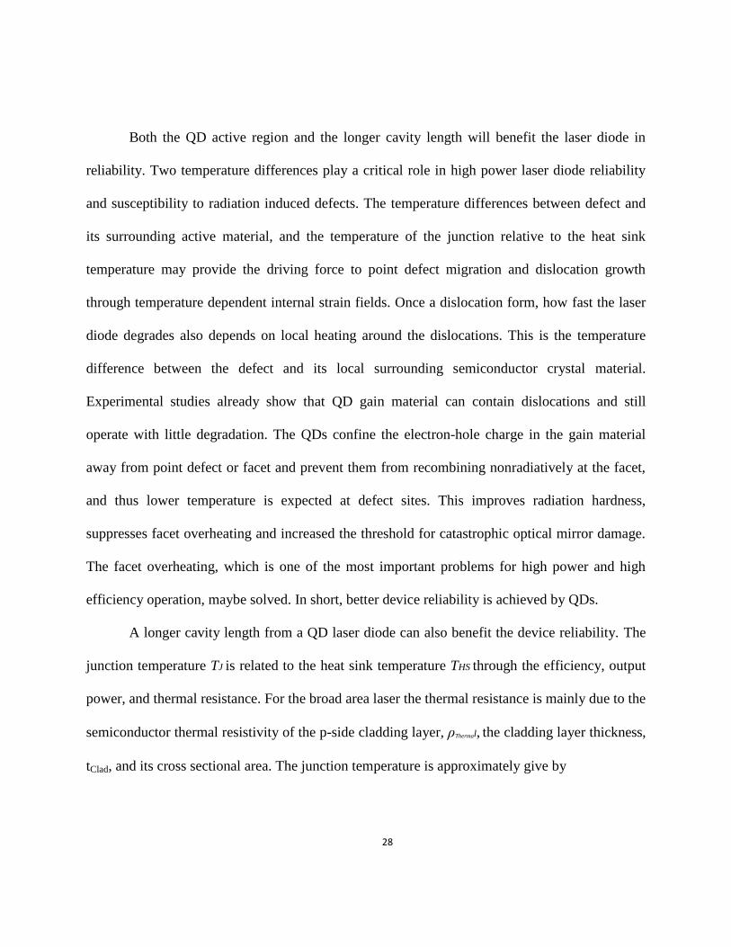
Figure 3-3: LI measurement of 0.5cm and 1cm by 100 μm devices at CW RT. .......................... 35
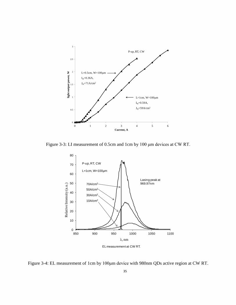
Figure 3-4: EL measurement of 1cm by 100μm device with 980nm QDs active region at CW RT.
.................................................................................................................................................. 35
Figure 3-5: EL measurement of 0.5cm by 100μm device with active region grown by thinner
InGaAs on GaAs at CW RT. The inserted chart is the expanded lasing spectrum. Spontaneous
emission is at 910nm and lasing is at 908.3nm. ....................................................................... 37

ix
Figure 4-1: Structure for oxide-free lithographic VCSEL. ........................................................... 41
Figure 4-2: Process flow of oxide-free lithographic VCSELs. ..................................................... 44
Figure 4-3: Output power versus injection current for devices with different mesa sizes. .......... 46
Figure 4-4: Comparison of LI and PCE of oxide-free lithographic VCSEL and commercial oxide
VCSEL from Princeton Optronics [59].................................................................................... 47
Figure 4-5: Spectrum of 5μm oxide-free lithographic VCSEL at different injection levels. ....... 47
Figure 4-6: Comparison of thermal resistance between oxide-free and oxide VCSELs .............. 50
Figure 4-7: Schematic of structure for intracavity contacts devices. ............................................ 51
Figure 4-8: Process flow for intracavity contacts devices. ........................................................... 52
Figure 4-9: Top view of device with intracavity n-contact. .......................................................... 53
Figure 4-10: IV (left) and LI (right) curves of 6μm devices with intracavity n-contact and
backside n-contact .................................................................................................................... 54

x
LIST OF TABLES
Table 2-1: Threshold and structure of three different samples ..................................................... 15
Table 2-2: Threshold current of devices with different width and mounting ............................... 19
Table 2-3: Threshold current and slope efficiency of devices with different cavity lengths ........ 21
Table 4-1: Characteristic of oxide-free lithographic VCSELs with different mesa sizes ............. 45
Table 4-2: Characteristics of 6μm devices with intracavity n-contact and backside n-contact .... 54

xi
LIST OF ACRONYMS/ABBREVIATIONS
AFM Atomic Force Microscopy
CTE Coefficient of Thermal Expansion
CW Continuous Wave
DI Deionized
EEL Edge Emitting Laser
EL Electroluminescence
FWHM Full Width Half Maximum
MBE Molecular Beam Epitaxy
PL Photoluminescence
QD Quantum Dot
QW Quantum Well
RT Room Temperature
RTA Rapid Thermal Annealing
SK Stranski-Krastanow
SML Sub Monolayer
VCSEL Vertical Cavity Surface Emitting Laser

1
CHAPTER 1 : INTRODUCTION ON LASER DIODE SELF-HEATING
Self-heating of a semiconductor laser limits the power conversion efficiency of the device.
The major heat sources in laser diodes are heating from optical free carrier absorption loss and
Joule heating from device electrical resistance. To control the seal-heating of a laser diode, the
epi structure must be designed to generate minimum dissipated power while the heat generated
must spread out of the device efficiently. To reduce heat generation, it is important to design the
active region and waveguide structure with low free carrier absorption loss and low electrical
resistance. In this section, a brief introduction on laser diodes self-heating mechanism is
introduced. Then, methods of reducing laser diode self-heating are discussed.
1.1 Laser diodes self-heating mechanism
Self-heating leads to temperature rise of laser diode and limits the output power,
efficiency and modulation bandwidth due to increased loss and decreased differential gain [1, 2].
The main heat sources in laser diode during continuous wave (CW) operation are Joule heating
and free carrier absorption loss.
As current is injected into the laser diode, Joule heating occurs due to semiconductor
material intrinsic resistance and the resistance at the heterojunction interfaces. The discontinuity
of band structure at heterojunction interface contributes a larger portion of the series resistance.
Holes have lower mobility than electrons so that p-type material has higher electrical resistance
than n-type layers. At the same time, free carrier absorption happens and generates hot carriers

2
during CW operation. The hot carriers interact with the lattice through phonon emission [3].
When the hot carriers relax to lower energy state, optical phonons are emitted. Lattice
temperature is increased when the optical phonons relax into acoustic phonons. Detailed studies
have shown that the quantum well (QW) active region temperature can be ~50˚C higher than the
cavity temperature during CW operation in edge emitting lasers (EELs) and vertical cavity
surface emitting lasers (VCSELs) as well [4, 5]. The temperature of QW carriers can be ~20˚C
higher than the lattice due to low optical phonon decay rate into acoustic phonons [5].
A lot of physical mechanisms in laser diode are affected at elevated active region
temperature. First of all, bandgap reduction happens leading to red shift of the gain peak (Figure
1-1). Fermi level also shifts and becomes closer to the barrier energy level causing wider Fermi
distribution of carriers [4]. As a consequence, carriers can be thermally ejected out of the QW
into the separate confined layers and peak gain is decreased substantially. Leakage of electrons
occurs and decreases the injection efficiency [1, 4-5]. To maintain the threshold gain, pump
power is increased. However, the differential gain is decreased due to broaden Fermi distribution
of carriers. Situation is more complicated in VCSELs. Gain spectrum shifts to longer wavelength
at a rate of ~0.27nm/˚C in GaAs based lasers while the cavity mode of VCSELs shifts 0.07nm/˚C
[6]. The misalignment between gain and cavity mode requires higher pump power to maintain
the threshold gain as well. Again, this will reduce the injection efficiency and differential gain.
When the carrier density is increased in the QW at higher pump level, stronger Auger
recombination and stronger spontaneous recombination occur since these processes depend on
the carrier density [4, 5]. Efficiency is further reduced by stronger spontaneous recombination.

3
Stronger Auger recombination adds up more heat to the active region. Free carrier absorption
also increases at higher carrier density and increases the internal optical loss. The decreased
injection efficiency and increased free carrier absorption loss will limit laser diode slope
efficiency. Finally, output power is limited by thermal rollover. It need to be point out that the
threshold current will also be increased at elevated temperature due to higher loss and lower
injection efficiency [7].
gain
gth
λ
gain
gth
λ
gain
gth
λ
EEL VCSEL
EFe
EFe
Low
junction T
High
junction T
gain
gth
λ
Cavity mode
Figure 1-1: Schematic of dynamic change of carrier distribution and gain at high junction
temperature.

4
1.2 Methods of reducing device self-heating
Joule heating and free carrier absorption loss are main heat sources in laser diodes. They
can take ~30% power consumption of commercial laser diode at maximum power conversion
efficiency operating point [8]. To reduce device self-heating, the design of laser epi structure
needs to be low resistance and low free carrier absorption loss. Since holes have lower mobility
and larger free carrier absorption cross section than electrons, optimization of p-type epi layers
are very important to reduce device self-heating.
Band discontinuity at heterojunctions causes large series resistance. To reduce the series
resistance, grading layers can be inserted and doping levels can be increased at heterojunctions.
However, one problem in optimization of the doping level is the trade-off between electrical
resistance and optical free carrier absorption loss. Higher doping level can reduce electrical
resistance while free carrier absorption loss is increased.
For VCSELs, the additional resistance above threshold is mostly in the DBRs [5]. Since
standing wave pattern forms in the cavity and DBRs, doping level can be increased at the nodes
of the cavity mode to reduce the electrical resistance while keep the free carrier absorption loss
low.
For EELs, the internal optical loss is given by
sjpjjnjjsji pn )( (1.1 )
where i is the total internal loss, j represents the confinement factor of the jth layer,
nj and pj are the free carrier scattering cross sections for electron and hole in that layer, jn and

5
jp are the electron and hole density, s is the loss related to the variation in the waveguide which
can be negligible since the modern technology allows the production of homogeneous high
quality epitaxial layers. Thus, the internal optical loss can take the form of
activeWGCLi (1.2)
where CL , WG and active are the loss of cladding, waveguide and active region respectively.
One possible way to reduce the internal loss is to increase the width of waveguide layer
[9]. In this way, a decrease in the penetration of the optical field into the cladding layers resulted
in the reduction of optical loss in CL while the reduction in the confinement factor of the active
region can minimize the active region loss active . Experimentally, Garbuzov et al [10] has shown
that devices with a broadened waveguide have lower internal loss than those with thinner
waveguide. As a result, 73A/cm2 per QW threshold current density and 1.3 cm
-1 internal loss are
achieved for 1.5μm laser diodes. One must notes that as the width of waveguide is increase, the
initial increase in carrier densities of the gain region is insignificant. However, the reduction of
confinement factor of the active region generally increases the threshold current density.
Another way to reduce the internal loss by engineering the waveguide design is to use
asymmetric waveguide design. Shifting the optical mode to n-cladding can decrease the cladding
loss since electrons have smaller free carrier absorption cross section than holes. Meanwhile,
active region loss can be reduced since the optical mode overlaps less with the gain region.
Theoretically, internal loss of 0.2cm-1
in a 4μm thick asymmetric waveguide at 1.08μm has been
predicted [11]. Experimentally, using asymmetric position of the QW in an ultrawide waveguide

6
to suppress higher order modes, internal loss of 0.34 cm-1
, CW output power of 16 W and
wallplug efficiency of 72% has been achieved in QW laser diodes [11].
A fundamental limitation in the minimization of internal optical loss is determined by the
free carrier absorption at the transparency carrier density in the active region. Figure 1-2 shows
the development of EELs in terms of threshold current density [12-27]. As shown in Figure 1-2,
Quantum dot (QD) lasers can reach lower threshold current density compared to QW lasers.
Threshold current density of 11.7A/ cm2 is reported by Deppe et al in 2008 [26]. The laser has a
single layer InAs QD active region with uncoated facets and 2cm long cavity. It is tested p-up
placed on copper heatsink without bonding and any additional heatsinking. 8.8A/cm2 is reached
in a 2 cm long device which is p-down mounted with bonding [27], which is the lowest threshold
current density achieved in any kind of semiconductor edge emitting lasers.
The 3-dimensinal quantum confinement of carriers in QD active region leads to discrete
energy level and delta-function density of states, which contributes to the decreased transparency
carrier density. As a consequence, self-organized QD gain material is able to reach very low
threshold current density. Very low internal loss can be achieved in a QD laser diode.
Experimentally, internal loss of ~0.25 cm -1
for QD laser diodes has been reported [27]. This is
the record low internal loss reported in literature for laser diodes at room temperature (RT) CW
operation. To further reduce seal-heating, devices with QD active region can be studied and
developed.
To control device self-heating, besides the low resistance and low free carrier absorption
epi structure design, the heat generated in the laser diode must spread out of the device

7
efficiently. To do so, the epi structure needs to be designed with low thermal resistance.
Applying efficient heatsinking can also increase the output power, power conversion efficiency
and modulation bandwidth [28, 29]. In this dissertation, thermal management of high power laser
edge emitting diodes using beryllium oxide (BeO) heatsink is introduced in Chapter 2. Chapter 4
demonstrates oxide-free lithographic VCSELs. Removing the oxide layer and using AlAs in the
DBRs leads to low thermal resistance in these VCSELs.
1980
Th
resh
old
Cu
rre
nt
De
nsity (
A/c
m2)
Development of laser threshold current density
20101990 2000 202019701960
1
10
100
1000
10000
100000 1st p-n junction lasers, ~10kA/cm2 , 77K,pulsed Holonyak, Hall, Quist, Nathan et al, 1962
1st RT CW DHS laser diode 940A/cm2 Alferov, 1970
1st QW laser operation at 15K, 36KA/cm2
optical pumped, Van der Ziel, 1975
1st injection , RT CW 3kA/cm2
Dupuis, 1978
GRINSCH 160A/cm2
Tsang, 1981
GRINSCH with SPSL40A/cm2
Alferov, 1988
1st QD laser, RT CW 950A/cm2
Kirstaedter , 1994
62A/cm2
Bimberg , 1997
DWELL,RT pulsed 26A/cm2
Liu , 1999 RT CW 19A/cm2
Deppe, 2000
17A/cm2
Sellers , 2004
11.7A/cm2
Deppe , 2008
8.8A/cm2
Deppe , 2009
p-n junction lasers
DH Laser
QW laser
QD laser1st RT DHS laser/pulsed4.3kA/cm2 Alferov, 1968
Figure 1-2: Historical evolution of edge emitting laser diodes threshold current density

8
CHAPTER 2 : LOW LOSS HIGH POWER QUANTUM WELL EDGE
EMITTING LASER DIODE AT 980NM
High power laser diodes at 980nm are important pumping sources for solid state lasers
and erbium-doped optical fiber amplifiers. Control self-heating is important to increase device
reliability and output power. A long cavity is essential to increase the gain for high power
operation. The waveguide must be designed with low free carrier absorption loss which enables
significant increase in cavity length without sacrificing the efficiency. In this section, the
asymmetric waveguide design and fabrication of the 980nm high power QW edge emitting laser
are introduced. Optimization of the waveguide and cladding material for better injection
efficiency is discussed. Using BeO heatsink to manage heat spreading and reach high output
power is talked. Injection efficiency of 71% and internal loss of 0.3 cm-1
have been achieved. For
the 0.5cm long device, a total output power of 9.3 W from both facets was measured at 14.5A
injection current which is limited by facet failing. Its power conversion efficiency goes up to
50 % and stays there close to the device’s facet failing.
2.1 Low loss asymmetric waveguide design and device fabrication
To reduce device self-heating, the waveguide is designed asymmetrically for low
internal loss. As shown in Figure 2-1, the p- and n- cladding layers are Al0.35Gas0.65As and
Al0.2Ga0.8As respectively. The waveguide is Al0.15Gas0.85As. A wider waveguide is helpful in
reaching low internal loss but high order modes tend to appear. Thus the width is kept at 1μm for
single mode operation. The active region is a single InGaAs QW designed at 980nm. Once the

9
waveguide structure, the fabrication steps, the thermal management and the facet coating are
optimized, replacing the QW active region with QDs may further reduce the internal loss and
improve the output power. The doping levels are optimized for low optical loss and low
electrical resistance. The calculated internal loss from equation 1.1 is only about 0.16cm-1
using
calculated carrier densities at equilibrium and assuming carrier densities are 1.5E18cm-3
in the
QW region. The measured loss is higher than the calculation because electro-hole build up in the
waveguide region under bias condition is different with that under equilibrium which will
increase the internal loss. The measurement of internal loss will be introduced later. As discussed
in Chapter 1, shifting the optical mode to n-cladding can decrease the cladding loss since
electrons have smaller free carrier absorption cross section than holes.
Figure 2-1: Simulation of the near field intensity of the waveguide mode and the design of the
laser structure.

10
The sample was grown on GaAs substrate using solid state molecular beam epitaxy
(MBE). It was fabricated into broad area laser diodes using the existing Ⅲ-Ⅴmaterial processing
technology. The fabrication procedures are illustrated in Figure 2-2. It starts from making the
120μm wide Chromium (Cr 200 Ȧ) /Gold (Au 1500Ȧ) stripe on top of the fresh semiconductor
surface. This step include spinning a layer of positive photo-resist AZ 5214 on the wafer surface
at 4000 rpm for 40 seconds and then baking it at 90 °C for 15 minutes in an oven. The stripe
openings are patterned through contact UV lithography using the designed mask and developed
in developer AZ 726 MIF for 45 sec. The wafer is dipped in the solution HCl: Deionized (DI)
H2O (1:1) for 5 sec to remove the oxide layer on sample surface before the metal deposition.
After metal deposition by thermal evaporation, metal lift-off is processed by immersing the
wafer in acetone.
The second step includes protection of the p-contact and epi-layers by sticking the epi-
side on glass slide with photo-resist AZ 5214 baked at ~110 °C for 10 minutes in an oven. Then
the back side of the wafer is etched in H2SO4:H2O2: DI H2O (4:1:1) for 20 minutes to etch off the
region that is damaged by Gallium loss during the high temperature growth so that the n-metal
will contact better and device resistance will be decreased. About 20μm of the back side GaAs is
etched off in this step. The wafer is then cleaned in acetone, isopropyl alcohol and DI water
consequently. Before the n-contact metallization, it was dipped into HCl: DI H2O (1:1) for 5 sec.
Then the n-contact of Germanium (Ge 200 Ȧ) /Gold (Au 1500Ȧ) is deposited by thermal
evaporation followed by the rapid thermal annealing (RTA) at 400 °C for 30 sec. The Ge
diffuses into GaAs during RTA and Ohm contact is formed.

11
Then, the p-metal is protected by lithographically patterned photo-resist stripes and the n-
metal is protected by sticking on glass slide with photo-resist baked at 90 °C for 10 minutes.
After the protection, the wafer is nonselective etched by H2SO4:H2O2: DI H2O (1:8:80) for 55 sec
to form a shallow etched mesa (ridge waveguide). The etch rate is about 65 Ȧ/sec to 110 Ȧ/sec
for GaAs and AlGaAs at RT. The heavily doped top layers are etched away in this step and
current confinement is achieved. The wafer is cleaned acetone, isopropyl alcohol and DI water
consequently after the etching.
Next, the p-contact is protected by patterned photo-resist stripes of 270μm in width. A
layer of 3500 Ȧ AlxOy is deposited by e-beam evaporation followed by lift-off in acetone with
ultrasonic wave. This layer of AlxOy is designed for better lateral current confinement especially
in the p-down mounted device. The region without AlxOy near the metal is designed for better
thermal conductivity.
Finally, a second p-metal of Cr 200 Ȧ /Au 1500Ȧ is deposited on top of the first p-metal
over the 270μm opening by lithography patterning, thermal evaporation of the metal and lift off.
The second metal is to prevent the gold/tin (Sn) solder from going into the semiconductor for the
p-down mounted device. The mounting will be discussed later.

12
Figure 2-2: Schematic of fabrication steps of the laser device
13
2.2 Optimization of waveguide and cladding material for better injection efficiency
High injection efficiency is important in reaching low threshold current and low internal
loss so that device self-heating can be reduced. The compositions of the waveguide and cladding
material are optimized to achieve high injection efficiency. The electrons are weakly localized in
a shallow QW since the binding energy of these electrons at room temperature is less than kT.
Thus, electrons are likely to emit into the waveguide which decreases the injection efficiency. A
higher Aluminum (Al) composition in the waveguide will make the QW deeper and increase the
electron confinement as well as the injection efficiency. However, a higher Al composition may
also increase the internal loss and nonradiative recombination in the waveguide due to decreased
crystal quality. Experiments are carried out to verify the best material composition for the
waveguide and cladding layers.
Table 2-1 shows the structures and device performance of three samples with different
waveguide and cladding layer materials. The p-cladding, waveguide and n-cladding for sample
702, sample 704 and sample 706 are Al0.3Ga0.7As/Al0.1Ga0.9As/Al0.15Ga0.85As,
Al0.35Ga0.65As/Al0.15Ga0.85As/Al0.2Ga0.8As and Al0.4Ga0.6As/Al0.2Ga0.8As/Al0.25Ga0.75As
respectively. QW position is 2000Ȧ away from the p-cladding in sample 704 and sample 706 for
higher gain while QW is placed 1000Ȧ away from the p-cladding in sample 702. Doping is
modified in different samples for lower loss. The less doped region at the inner part of the p-
cladding of sample 702 and 704, and the undoped p-side waveguide in all three samples are for
lower hole absorption loss. The high doped n-side waveguide region in sample 702 and 704 is

14
designed to prevent holes from going there so that the injection efficiency maybe better and the
nonradiative recombination as well as hole absorption loss in the waveguide will be reduced.
Table 2-1 also shows the measured threshold current and threshold current density of
these samples. The measured L-Is of 1cm long devices are illustrated in Figure 2-3. The devices
are cleaved into 0.5cm, 1 cm and 1.5 cm long cavity lengths and operated at CW room
temperature with cleaved facets only. The devices of sample 704 and 706 are fabricated as
describe above except that they have first p-metal of 50μm and second p-metal of 120μm.
Sample 702 has first p-metal of 50μm and AlxOy is opened 50μm above the metal, while the
second p-metal is everywhere on top of the first metal and AlxOy.
The best devices are from sample 704 with low threshold current density and high slope
efficiency. Sample 702 has similar slope but higher threshold current compared with sample 704
indicating that the QW carrier confinement in the structure of 702 is not as good as that in
sample 704. Sample 706 has lower threshold than sample 702 (still higher than sample 704) but
the slope efficiency is much worse indicating higher internal loss in the waveguide of sample
706.
15
Table 2-1: Threshold and structure of three different samples
Device Ith (A) Jth (A/cm2) Ith (A) Jth (A/cm2) Ith (A) Jth (A/cm2)
0.5cm 0.63 251 0.40 158 0.55 219
1cm 0.86 173 0.67 135 0.71 142
1.5 cm 1.20 160 0.87 116 NA NA
P cladding
1μmWG
N cladding
QW position
p side WG
702 CW mode 704 CW mode 706 CW mode
30%AlGaAs
10%AlGaAs
15%AlGaAs
35%AlGaAs
15%AlGaAs
20%AlGaAs
40%AlGaAs
20%AlGaAs
25%AlGaAs
1000A from p cladding 2000A from p cladding 2000A from p cladding
inner 3000A 2E17cm-3inner 3000A 5E17cm-3
undoped undoped undoped
inner 100A 5E17 cm-3
p cladding others 1E18 cm-3 others 1E18 cm-3
all 1E18 cm-3
others 1E16 cm-3n side WG
inner 50A 1E17cm-3
others 1E16 cm-3
inner 2000A undoped
others 1E16 cm-3
Figure 2-3: L-Is of devices from sample 702, 704 and 706 with 1cm long cavity length.

16
2.3 Thermal management using BeO heatsink and wider metal stripes
To control device self-heating, the heat generated in the device must be carried out
efficiently. As can be seen from the previous measured L-Is of sample 704, although it has the
best performance among the three different samples, the output power is still limited by thermal
rollover at high injection current. The heat generated in active region, free carrier absorption or
nonradiative recombination can reduce the gain, differential gain, slope efficiency, output power
and degrade the reliability. Thus, thermal management is very important to improve laser
performance and reliability.
The temperature difference between heat source and heat sink is dissThermal PRT ,
where opticalelectricaldiss PPP . ,ΔPdiss, Pelectical and Poptical, is the dissipated electrical power,
electrical input power and optical output power. A lower thermal resistance means the device can
spread the dissipated power more efficiently and temperature rise will be smaller in the active
region (a lower junction temperature). Using a wider stripe at a given cavity length will reduce
the thermal resistance.
Another way to get better heat spreading is to apply a heat sink onto the laser diode
using p-down mounting. This is because the GaAs substrate contributes most of the thermal
resistance due to its large thickness and relatively low thermal conductivity (~50W/mK [30]).
The back side etching during fabrication of the device can decrease the thermal resistance and
finally the junction temperature. But that is not enough. The active region is much closer to the
p-side surface which is only a few microns away from the active region while the substrate is

17
usually hundreds of microns thick. In p-down mounted devices, waste heat can dissipate through
the p-side waveguide, cladding and p-metal contact efficiently due to lower thermal resistance
and short distance from the heat sink. The waste heat is finally spread through the contact to heat
sink.
To apply the heat sink onto the device for p-down mounting, the coefficient of thermal
expansion (CTE) mismatch between laser diode and heatsink must be considered [29]. Stain
caused by CTE mismatch will degrade device performance and lifetime. GaAs has CTE of
~5.8x10⁻⁶
/K. Typically, CTE of 6x10⁻⁶
/K to 9x10⁻⁶
/K is acceptable to match GaAs [31]. Thus,
the BeO heat sink from Applied Thin-Film Products with CTE of ~8x10⁻⁶
/K and high thermal
conductivity of ~330W/mK is selective as the heatsink to match with GaAs.
To spread heat efficiently through heatsink, a thin void-free mechanical contact between
laser diode and heatsink is required. As illustrated in Figure 2-4, Gold/Tin (Au80Sn20) hard
solder is predeposited onto the center of the BeO heatsink from Applied Thin-Film Products for
solder joint. Au/Sn eutectic alloy is stiff, free from thermal fatigue and has good thermal
conductivity (~57W/mK). The BeO heatsink is 2cm long and 1 cm wide. TiW/Au is also
predeposited on both sides of the BeO heatsink.
The device is carefully aligned on the Au/Sn solder with the output facet close to the edge
of the heat sink allowing good heat spreading away from the facet. It is very important to form
void-free bonding interface in the mounting process because voids can lead to heat spots. It
blocks heat flow and increases thermal resistance. Voids can also degrade the electrical and
mechanical properties of the bonding [29]. To reduce the chance of void formation, a force of
18
100g is applied and the whole assembly was being heated up to 280 °C which is the melting
point of the Au/Sn solder during the mounting process. The force applied to the laser diode is
minimized due to the melting stage of the solder to reduce the bonding stress. Indium (In) solder
is used to bond the BeO onto copper block heatsink which is used in the experiment setup for
measurement. The reason that the laser diode is not bonded to the cooper heatsink directly using
In solder is due to the larger CTE mismatch between copper (~17x10-6
/K) and GaAs (5.8x10⁻⁶
/K).
In solder is also soft and tends to contaminate the laser facets.
Pre-patterned Au/Sn Solder
Pre-deposited TiW/Au
Pre-deposited TiW/Au
Substrate: BeO heat sink
Figure 2-4: Schematic of BeO heat sink and packaging of the laser diode on heat sink. The laser
diode is mounted p-down onto the BeO heat sink using Au/Sn solder. The BeO heatsink is
mounted with Indium solder onto a copper heat sink.
Figure 2-5 shows the measured LIs of two 1 cm long devices from sample 704 with
different stripe widths. The threshold currents are shown in Table 2-2. The 50μm wide device is

19
not mounted and measured p-up on top of copper heatsink without bonding. The 120μm wide
device is mounted on BeO heatsink as described above and tested p-down. The 50μm wide
device has a higher threshold current density. Its output optical power is limited by thermal
rollover at a driven current above 1.3A, while the 120μm wide p-down mounted device has a
lower threshold current density and the output power is not limited by thermal rollover up to 2 A.
The comparison indicating that the 120μm wide p-down mounted device has lower thermal
resistance and waste heat is spread efficiently out of the device resulting in lower junction
temperature.
Table 2-2: Threshold current of devices with different width and mounting
704 CW mode 1cm Long Ith (A) Jth (A/cm2)
W=50um unmounted 0.67 134W=120um p-down mounted 1.1 92
0
50
100
150
200
250
300
0.0 0.5 1.0 1.5 2.0
Ph
oto
po
we
r [m
W]
Current [A]
CW RT p-up unmounted 50un wide
CW RT p-down mounted 120um wide
Figure 2-5: L-Is of 1 cm long device from sample 704 with different width and mounting

20
Further measurements of the 120μm wide p-down mounted devices show that the devices
can reach out put optical power of 4 W at CW room temperature from two cleaved facets. This is
illustrated in Figure 2-6. The measurements are limited by the driven current source to 8 A
injection current. The 0.5 cm long device starts to degrade at input current higher than 6A and
output power higher than 4W limited by facet overheating.
The threshold current density and slope efficiency of these devices are listed in Table 2-3.
The longer devices have lower threshold current density because the threshold current depends
on the amount of gain that is required to reach lasing which is set by the loss of the cavity. The
loss of the cavity includes the internal loss from free carrier absorption in different layers and the
external optical loss via )1
ln(1
BF
extRRL
. RF and RB are the reflectivity of front and back facet.
Therefore the cavity loss decreases as the cavity length becomes longer in the case that the
internal waveguide distributed loss is sufficiently small. Thus, the longer cavity device will have
a lower threshold current density. This can also indicated the internal loss of these devices is
small.

21
0
0.5
1
1.5
2
2.5
3
3.5
4
4.5
5
0.0 1.0 2.0 3.0 4.0 5.0 6.0 7.0 8.0
Ou
tpu
t po
wer
[W
]
Injection Current [A]
sample # 704, CW RT
2cm long device
1.5cm long device
1cm long device
0.5cm long device
Figure 2-6: L-Is of 120μm wide p-down mounted devices for two facets without coating from
sample 704 with different cavity length.
Table 2-3: Threshold current and slope efficiency of devices with different cavity lengths
Cavity Length (cm) Ith(A) Jth(A/cm2) ηd slope efficiency 1/ηd
0.5 0.60 100 63% 1.58
1 1.10 92 57% 1.76
1.5 1.57 87 46% 2.18
2 1.95 81 35% 2.88
From the differential slope efficiency of the devices at different cavity lengths, one can
also calculate the injection efficiency and internal loss of the devices. The slope efficiency is
usually given by

22
LR
InR
In
RIn
RIn
bf
bf
id
2)1
()1
(
)1
()1
(
( 2.1 )
where Rf and Rb are the reflectivities of the front and back facets, α is internal loss, L is
cavity length, ηi is injection efficiency. Here, the internal optical loss and the injection efficiency
are assumed to be independent of bias conditions and temperature. The inverse differential slope
efficiency is then:
)1
(
)1
()1
(
)1
(
21
f
i
bf
f
id
RIn
RIn
RIn
L
RIn
( 2.2 )
In our case Rf = Rb = R since there is only cleaved facets, which gives inverse slope
efficiency for two facets:
i
id
L
RIn
1
)1
(
1 ( 2.3 )
If the assumption that internal optical loss and injection efficiency are independent of
bias conditions and temperature is true, the inverse differential slope efficiency is expected to fall
on a straight line against cavity length L. One can get the injection efficiency of the devices from
the value of inverse differential slope efficiency at zero cavity length throughB
i
2 , where B is
the inverse differential slope efficiency at zero cavity length. The internal loss can be calculated
using the slope of the straight line and the calculated injection efficiency through
23
2
)1
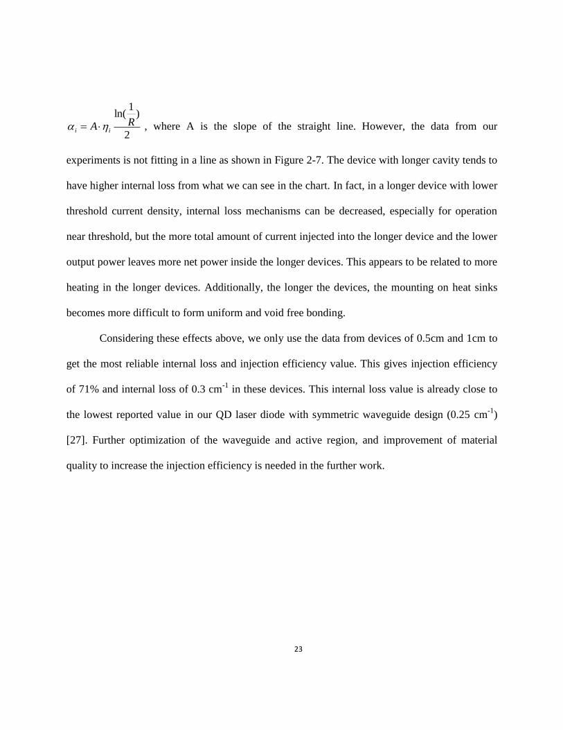
ln(RA ii , where A is the slope of the straight line. However, the data from our
experiments is not fitting in a line as shown in Figure 2-7. The device with longer cavity tends to
have higher internal loss from what we can see in the chart. In fact, in a longer device with lower
threshold current density, internal loss mechanisms can be decreased, especially for operation
near threshold, but the more total amount of current injected into the longer device and the lower
output power leaves more net power inside the longer devices. This appears to be related to more
heating in the longer devices. Additionally, the longer the devices, the mounting on heat sinks
becomes more difficult to form uniform and void free bonding.
Considering these effects above, we only use the data from devices of 0.5cm and 1cm to
get the most reliable internal loss and injection efficiency value. This gives injection efficiency
of 71% and internal loss of 0.3 cm-1
in these devices. This internal loss value is already close to
the lowest reported value in our QD laser diode with symmetric waveguide design (0.25 cm-1
)
[27]. Further optimization of the waveguide and active region, and improvement of material
quality to increase the injection efficiency is needed in the further work.

24
1.4
1.6
1.8
2
2.2
2.4
2.6
2.8
3
0 0.5 1 1.5 2
inve
rse
dif
eren
tial
slo
pe
effi
cien
cy
Cavity length [cm]
Figure 2-7: Inverse differential slope efficiency against cavity length
Figure 2-8 shows measurements up to higher injection currents of a device that is 0.5 cm
long with 120 µm stripe width, p-down mounted on a BeO heat sink without any facet coating. A
total output power of 9.3 W from both facets was measured at 14.5A injection current which is
limited by facet heating. The power conversion efficiency goes up to 49.4 %. No thermal
rollover is observed until the facet failing. It indicates that the p-down mounted device has low
thermal resistance and waste heat can spread out of the device efficiently.

25
0%
10%
20%
30%
40%
50%
60%
0.0
2.5
5.0
7.5
10.0
0.0 2.5 5.0 7.5 10.0 12.5 15.0
Po
wer
Co
nve
rsio
n E
ffic
ien
cy
Ou
tpu
t Po
wer
[W]
Injection Current (A)
sample # 704
Mounted p-downL=0.5cm, W=120 µm
Ith=0.6A, Jth=100A/cm2
PCEmax =49.4% at 5.5APmax=9.3W at 14.5A from 2 facets
Figure 2-8: CW RT output optical power and power conversion efficiency vs. injection current
of device with 0.5cm long and 120 µm wide ridge waveguide, measured p-down mounted on
BeO heatsink without facet coating.

26
2.4 Summary
Low internal loss is important to reduce device self-heating for high power laser
operation. The laser diode with asymmetric waveguide design can reach very low internal loss.
The optimized waveguide and cladding material composition increases the injection efficiency
and reduces the threshold current. P-down mounted devices on BeO heatsink with wider metal
stripe have lower thermal resistance. These devices have injection efficiency of 71% and internal
loss of 0.3cm-1
. At 14.5A injection current, 9.3W total optical power from both facets is
measured from p-down mounted 0.5cm long device.

27
CHAPTER 3 : LOW THRESHOLD DEVICE WITH QUANTUM DOTS
ACTIVE REGION
3.1 Introduction of QD edge emitting laser at 980 nm
Commercial high power laser diodes at 980nm are QW lasers. The aim of this research is
to develop a high power QD edge emitting laser to improve the output power and reliability in
980 nm high power diode lasers. QD lasers are believed to have advantages over the QW lasers
in terms of decreased transparency carrier density, increased material gain and large
characteristic temperature T0. The low transparency carrier density of the QD active region
makes it possible to reach a very low threshold current density [27]. As a result, the internal loss
can be reduced since the free carrier absorption loss is the major loss mechanism in laser diodes
with high quality epitaxial layers. Both low threshold current density and low internal loss are
important to make high power laser diodes with long cavities. Experimentally, it has shown that
QDs lasers are promising for high power applications at 980nm [32, 33].
A major factor that limits the maximum output power of the laser diode is the cavity
length. To reach lasing with long cavity length requires low internal loss and excellent thermal
management. QD transparency carrier density is order of magnitude lower than the QW active
region because of the discrete density of states. As shown in the previous review section, QD
active region is able to achieve low threshold current density and low temperature sensitivity due
to low transparent carrier density, which in turn results in low internal loss and low resistive loss
as well. With carefully design of the waveguide and optimization of doping levels in the
claddings, QD laser diodes at 980nm will be promising to have very low internal loss.
28
Both the QD active region and the longer cavity length will benefit the laser diode in
reliability. Two temperature differences play a critical role in high power laser diode reliability
and susceptibility to radiation induced defects. The temperature differences between defect and
its surrounding active material, and the temperature of the junction relative to the heat sink
temperature may provide the driving force to point defect migration and dislocation growth
through temperature dependent internal strain fields. Once a dislocation form, how fast the laser
diode degrades also depends on local heating around the dislocations. This is the temperature
difference between the defect and its local surrounding semiconductor crystal material.
Experimental studies already show that QD gain material can contain dislocations and still
operate with little degradation. The QDs confine the electron-hole charge in the gain material
away from point defect or facet and prevent them from recombining nonradiatively at the facet,
and thus lower temperature is expected at defect sites. This improves radiation hardness,
suppresses facet overheating and increased the threshold for catastrophic optical mirror damage.
The facet overheating, which is one of the most important problems for high power and high
efficiency operation, maybe solved. In short, better device reliability is achieved by QDs.
A longer cavity length from a QD laser diode can also benefit the device reliability. The
junction temperature TJ is related to the heat sink temperature THS through the efficiency, output
power, and thermal resistance. For the broad area laser the thermal resistance is mainly due to the
semiconductor thermal resistivity of the p-side cladding layer, ρThermal, the cladding layer thickness,
tClad, and its cross sectional area. The junction temperature is approximately give by

29
o
HSPCE
HSPCE
gstripe
CladThermalHSo
HSPCE
HSPCEThermalHSJ P
T
T
LW
tTP
T
TRTT
)(
)(1
)(
)(1
( 3.1 )
Wstripe is the stripe width, Lg is the gain length, ηPCE is the power conversion efficiency, Po
is the output power, Rthermal is the thermal resistance. For a given heat sink temperature, strip
width and cladding layer thickness, the thermal resistance and junction temperature can be
reduced if the cavity length can be increased without reducing the power conversion efficiency.
This cavity length can be increased to a length set by the internal optical loss before the power
conversion efficiency drops significantly. Owing to a low operating current density and the
reduced junction temperature in longer device, reduction of the internal heating at defects can be
achieved. Again this will improve radiation hardness and the reliability of the laser diodes.

30
3.2 Growth of QDs active region at 980nm
To further reduce the device internal loss and self-heating, devices with QD active region
is studied. We tried a method of alternating sub monolayers (SML) deposition initially to grow
the 980nm QDs active region. It has been reported that the deposition of a short-period
InAs/GaAs superlattice on a GaAs (100) surface, with an InAs effective thickness of less than 1
monolayer, results in the formation of nanometer scale (In,Ga)As QDs of a non-Stranski-
Krastanow (SK) class [34]. In the alternating SML deposition, sub monolayers of InAs are being
deposited between GaAs layers. Strain effects cause the InAs to migrate and form InAs rich
regions. With this method the wavelength can be controlled to some degree by the amount of
GaAs that is used in between the InAs layers.
Although very good photoluminescence (PL) results have been obtained by SML
deposition QDs, these QDs suffer from interdiffusion during the growth of the upper waveguide
and p-cladding layers. High growth temperature is needed for the cladding and waveguide layers
of the laser structures to achieve the best material quality because it insures that the material
grows with fewer defects. The increasing Al concentration in waveguide and cladding can also
increase the As antisite defects and modify either the incorporation or the concentration of
oxygen contaminants. At the higher growth temperatures, either the AlGaAs incorporates less
oxygen due to increased thermal desorption or the oxygen contaminants incorporate differently.
However, in either case the AlGaAs appears to have reduced nonradiative recombination and the
interfaces will be smoother. At relatively low growth temperatures, the waveguide interfaces are

31
smooth but the nonradiative recombination rate is high so that the injection efficiency will be
low. At growth temperature in the middle level, interfaces will be rough. Optical loss will be
increased due to increased scattering loss at the waveguide interfaces.
Thus, high temperature is essential to grow waveguide and cladding layers with best
material quality. This is not a problem for the n-side layers since they are grown prior to the QDs
which can be grown at its optimum temperature using temperature ramps. However, to grow the
p-side layers after the active region with best material quality at high temperature,
experimentally, the SML QDs is found to suffer from interdiffusion and can not match the
growth condition of p-side layers.
A method of growing bulk InGaAs material on GaAs is studied to form stable QDs using
the SK growth mode. In this way, InGaAs is grown on GaAs and QDs with emission at 980nm
forms due to strain effects by tuning the In composition and InGaAs layer thickness. Figure 3-1
shows the atomic force microscopy (AFM) image of the InGaAs QDs forms on GaAs. The AFM
measurement shows that these QDs have height about 6nm and width about 50nm. The height
and width varies between the dots. QDs density is 2E10cm-2
.

32
Figure 3-1: AFM image of the InGaAs QDs with height~6nm and width ~50nm. QDs density
2E10cm-2
.

33
3.3 Test of device with 980nm QDs active region
Laser sample with similar waveguide and cladding design as described before has been
grown with 980nm InGaAs QDs active region. To increase the gain, the waveguide is designed
symmetrically. Figure 3-2 shows the PL measurement of a laser sample with the InGaAs QDs
active region at RT and 78K. The PL measurement shows the active region emits at 985nm with
a line width of 92.2meV at RT. The emission shifts to 946nm with a line width of 58.3meV at
78K. The wide full-width-half-maximum (FWHM) at 78K indicating the inhomogeneous
broaden of the QDs emission due to size non-uniformity.
0
0.2
0.4
0.6
0.8
1
1.2
800 850 900 950 1000 1050 1100
rela
tiv
e in
ten
sity
, a
u.u
.
λ,nm
PL of QDs
T=77K
λ=946nm
FWHM
58meV
T=300K
λ=985nm,
FWHM
92meV
Figure 3-2: PL result of a sample with In0.33Ga0.67As QDs active region, with peak wavelength
985nm/946nm and line width 92.2meV/58.3meV at RT and 78K

34
The samples were made into laser devices and tested. All devices have 100μm wide
stripes and were tested p-up at CW RT. Figure 3-3 shows the measured LI of the 0.5cm and 1cm
long devices. 1cm long device has threshold current of 0.59A (59A/cm2) and the 0.5cm long
device has threshold current of 0.36A (71A/cm2). It can be seen that the devices with longer
cavity length have lower threshold current density indicating that the device has low internal loss.
However, the internal loss and injection efficiency can not be calculated from the measurement
since the output power of the p-up measurement is limited by heating and the devices from this
sample has high voltage due to not optimized waveguide structure and doping level. By
measuring the electroluminescence (EL) of both the 0.5cm and 1 cm long devices, it shows that
both devices has spontaneous emission at ~980nm with line width of ~60meV. The emission is
from ground states of the QDs which coincides with the PL test. Both devices have lasing peak
wavelength shorter than the spontaneous emission peak. The shorter lasing peak wavelengths
than the spontaneous emission peak indicating that the QDs are not uniform and the lasing is not
at ground state of the QDs active region. Optimization of the growth condition of QDs needs to
be studied to grow the QDs more uniformly and make the lasing at ground state.
35
0
0.5
1
1.5
2
2.5
3
0 1 2 3 4 5 6
lig
ht
ou
tpu
t p
ow
er,
W
Current, A
L=0.5cm, W=100μm
Ith=0.36A,
Jth=71A/cm2
L=1cm, W=100μm
Ith=0.59A,
Jth=59A/cm2
P-up, RT, CW
Figure 3-3: LI measurement of 0.5cm and 1cm by 100 μm devices at CW RT.
EL measurement at CW RT.
0
10
20
30
40
50
60
70
80
850 900 950 1000 1050 1100
Rel
ati
ve
Inte
nsi
ty (a.u
.)
λ, nm
P-up, RT, CW
L=1cm, W=100μm
70A/cm2
50A/cm2
30A/cm2
10A/cm2
Lasing peak at
969.97nm
Figure 3-4: EL measurement of 1cm by 100μm device with 980nm QDs active region at CW RT.
36
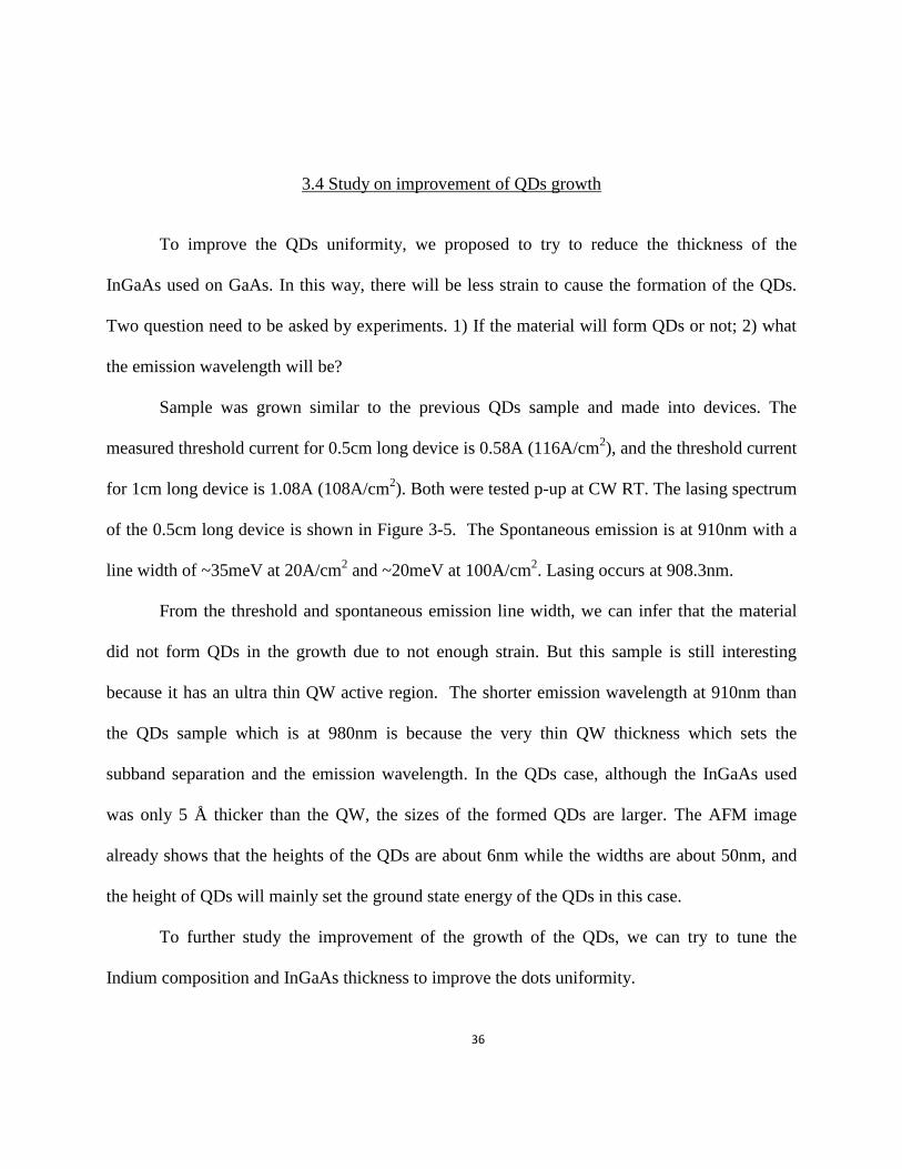
3.4 Study on improvement of QDs growth
To improve the QDs uniformity, we proposed to try to reduce the thickness of the
InGaAs used on GaAs. In this way, there will be less strain to cause the formation of the QDs.
Two question need to be asked by experiments. 1) If the material will form QDs or not; 2) what
the emission wavelength will be?
Sample was grown similar to the previous QDs sample and made into devices. The
measured threshold current for 0.5cm long device is 0.58A (116A/cm2), and the threshold current
for 1cm long device is 1.08A (108A/cm2). Both were tested p-up at CW RT. The lasing spectrum
of the 0.5cm long device is shown in Figure 3-5. The Spontaneous emission is at 910nm with a
line width of ~35meV at 20A/cm2 and ~20meV at 100A/cm
2. Lasing occurs at 908.3nm.
From the threshold and spontaneous emission line width, we can infer that the material
did not form QDs in the growth due to not enough strain. But this sample is still interesting
because it has an ultra thin QW active region. The shorter emission wavelength at 910nm than
the QDs sample which is at 980nm is because the very thin QW thickness which sets the
subband separation and the emission wavelength. In the QDs case, although the InGaAs used
was only 5 Å thicker than the QW, the sizes of the formed QDs are larger. The AFM image
already shows that the heights of the QDs are about 6nm while the widths are about 50nm, and
the height of QDs will mainly set the ground state energy of the QDs in this case.
To further study the improvement of the growth of the QDs, we can try to tune the
Indium composition and InGaAs thickness to improve the dots uniformity.

37
EL of sample 783 L=0.5cm Device CW RT
0
50
100
150
200
250
300
800 850 900 950 1000
Wavelength (nm)
Inte
nsit
y (
a.u
.)
0.1A CW 100/200um
0.3A CW 100/200um0.5A CW 100/200um
0.6ACW 5/10um
EL of sample 783 L=0.5cm Device I=0.6A CW RT slits 5/10um
0
50
100
150
200
250
300
907 907.5 908 908.5 909
wavelength (nm)
Inte
nsit
y (
a.u
.)
Figure 3-5: EL measurement of 0.5cm by 100μm device with active region grown by thinner
InGaAs on GaAs at CW RT. The inserted chart is the expanded lasing spectrum. Spontaneous
emission is at 910nm and lasing is at 908.3nm.
3.5 Summary
Growth of 980nm QDs with bulk InGaAs on GaAs has been studied, and laser samples with
980nm QDs active region have been made into devices and tested. 1cm long device has threshold
current of 59A/cm2 which is the lowest value reported in literature for QD lasers at 980nm to our
best knowledge. Optimization the 980nm QDs active region growth condition needs to be further
studied to form uniform dots for ground state lasing. Once the waveguide design and QDs active
region are optimized, further reducing the threshold current density and even lower internal loss
can be expected.

38
CHAPTER 4 : OXIDE-FREE LITHOGRAPHIC VCSEL
4.1 Introduction on vertical cavity surface emitting lasers
Vertical Cavity surface emitting laser was first proposed by Dr. Kenichi Iga in 1977 [35].
A typical VCSEL consists of an optical cavity spacer of multiple half wavelengths thick with
QW or QD active layers at the antinodes of the cavity mode. Top and bottom DBR mirrors with
very high reflectivity (R>99%) provide optical feedback. This layout offers VCSELs many
inherent advantages over the edge-emitting lasers. 1) The symmetrical laser beam emission with
small divergence angle allows efficient coupling to optical fibers. 2) Single longitudinal mode
operation is achieved due to large mode separation of the short cavity length. 3) Low threshold
operation is expected from its small gain volume. 4) Large relaxation frequency enables high
speed modulation. 5) It enables high-volume, low-cost wafer scale fabrication and test. 6)
Densely packed two-dimensional (2-D) laser arrays can be formed. VCSELs play an important
role in data communications, pump lasers, sensors and computer mice.
Iga and coworkers reported the first device in 1979 [36]. The first device had metallic
mirrors and GaInAsP-InP double heterostructure as the active region. It was driven under pulse
mode at liquid-nitrogen temperature, with lasing wavelength of 1.18μm and high threshold
current of 900mA (11kA/cm2). Room temperature pulse operation was realized using
GaAlAs/GaAs system at 874nm in 1984 with threshold current of 510mA [37]. First RT CW
operation of a VCSEL was reported in 1989 with a GaAs active region (Ith~36mA) [38].

39
However, it still needs high reflectivity mirrors to provide enough feedback and reduce the
threshold. With the development of crystal growth techniques of MBE and metal organic
chemical vapor deposition (MOCVD), semiconductor distributed Bragg reflectors (DBRs) were
incorporated into VCSELs since late 1980s [39, 40], which made low threshold current possible.
To design high efficient VCSELs, it is very important to achieve high efficient transverse
current and optical mode confinement. Historically, there are several developed confinement
technologies that aims at improving device efficiency. The etched-post structure [41] suffers
optical scattering loss from the imperfections in the semiconductor/air interface and carrier loss
due to surface recombination at the side wall as well as carrier lateral diffusion in the active
region [42, 43]. Highest wall plug efficiency achieved by this kind of devices is only 17.3% [44].
The once commercialized proton implanted VCSELs [45] lack index guiding. It is also difficult
to control the implant depth, position and size. The implanted region must be away from the
active region to avoid damage, but this introduces undesirable current spreading. Wall-plug
efficiency of 28% has been achieved in proton implanted devices [46].
The most successful confinement technology that dominates in commercial VCSELs is
the oxide confinement [47, 48]. At elevated temperature, a chemical instable high Al content
AlGaAs layer is converted into transparent native oxide by reaction with water vapor [49]. The
oxide layer is an insulator and can be placed closer to the active region than the ion implanted
structure. This reduces current spreading and results in good current confinement. It also has a
low refractive index about 1.6 while original semiconductor layer has a typical refractive index
of ~3. In other words, optical confinement is achieved by index guiding. Oxide VCSELs have

40
achieved very low threshold current of 8.7μA [50]; high wall-plug efficiency of 57% at 850 nm
[51] and 62% at 1062 nm [52]; and modulation bandwidth higher than 20 GHz with modulation
speed higher than 40Gbit/s [53].
However the oxide-confine VCSELs are not yet perfect due to the problems associated
with the oxide-aperture formation. Thermal resistance, internal strain field and size variation
limit the performance and productivity of VCSELs.
The oxidation process introduces dislocation and defects at the oxide and semiconductor
interface [54]. The volume change during oxidation creates strain field. The deferent thermal
expansion coefficients of the oxide and semiconductor add up to the strain field and degrade the
device reliability. The defects can be driven by strain field to migrate towards the active region
where the defects act as non-radiative recombination centers and kill the device. The AlxOy has a
low thermal conductivity of 0.7W/mK while GaAs and AlAs have thermal conductivity of
~50W/mK and ~110W/mK respectively [30]. Heat is blocked by the oxide and heat spreading
from the upper semiconductor DBRs is limited. Device self-heating limits the maximum output
power and saturate modulation speed [55]. Smaller devices suffer more from self-heating
problem because higher resistance generates more Joule heat and smaller aperture limits upward
heat flow. The wet oxidation is a diffusion process. Poor size control and un-uniformity limit the
reproducibility for manufacturing especially for small devices.
To solve all these problems in oxide VCSELs, an oxide-free lithographically-defined
VCSEL has been under developing recently [56] (Figure 4-1). A carefully designed intracavity
lithographically-defined phase-shifting mesa is introduced for optical confinement. The current

41
confinement is achieved only by engineering the design and growth of the mesa and cavity
spacer. To do so, the oxide aperture and internal strain field are eliminated. Device can be more
reliable with lower thermal resistance. Less self-heating will increase the maximum output
power and modulation speed of the device. Lithography technology inherently provides excellent
scaling and uniformity throughout the wafer, which increases device reproducibility and yield.
Cost in manufacturing can be reduced to make oxide-free lithographic VCSELs.
Figure 4-1: Structure for oxide-free lithographic VCSEL.

42
4.2 Device design and fabrication
There are some rule of some principals to design high efficient VCSELs. First, the cavity
mode needs to be tuned to match the QW emission gain. The lasing wavelength of VCSEL is
determined by the cavity and DBRs. At higher temperature, cavity mode shifts to longer
wavelength due to thermal expansion (~0.07nm/K), while the gain shifts much faster to the
longer wavelength due to bandgap reduction (~0.27nm/K). Shifting the cavity mode to longer
wavelength side of the gain peak can compensate the misalignment at high temperature so that
device self-heating is compensated to improve the output power at high driving level.
The DBRs must to be designed with high reflectivity to provide enough feedback while
the resistance and optical loss need to be low to limit device self-heating and improve the overall
efficiency. To reduce device resistance and free carrier absorption loss, grading layers are
inserted at heterojunction interfaces and doping levels are modified. One benefit from the
elimination of wet oxidation in lithographic VCSEL design is that AlAs/GaAs can be used in the
DBRs instead of AlGaAs DBRs which has lower thermal conductivity due to alloy scattering of
phonons [57]. This can further reduce the device thermal resistance and limit device self-heating.
It is most important to engineer on the design and growth of the intracavity phase shifting
mesa and cavity spacer to achieve efficient current confinement. Based on these design
principals, the cavity mode, band structure, DBR reflectivity and loss are simulated. Then,
sample is grown and fabricated into devices. Based on feedback from testing, design is modified.
As these procedures go on, the VCSEL structure is optimized.

43
The fabrication of the oxide-free lithographic VCSELs is straight forward as shown in
Figure 4-2. The first growth starts on GaAs n+ substrate and stops at the first pair of the top
DBRs. Grading layers are inserted and doping level is modified to flatten the band discontinuity.
Then 1-λ thick AlGaAs cavity spacer is grown with three QWs in the center separated by GaAs
barrier layers. The emission wavelength is designed at 980nm. After the first growth, phase
shifting mesas are defined by lithography and wet etching. Lithography scales the mesa sizes
from 1μm to 6 μm. Scaling properties can be studied by measuring devices with different mesa
sizes. Then, sample is reloaded to the MBE to perform the regrowth of the p-type AlAs/GaAs top
DBRs. Grading layers are also inserted and doping level is modified as well. After the regrowth,
Cr/Au p-metal is deposited and lifted off, followed by Ge/Au n-metal deposition and annealing
at the back side of the sample. In the end, devices will be isolated by wet etching and tested
afterwards.

44
Figure 4-2: Process flow of oxide-free lithographic VCSELs.

45
4.3 High power conversion efficiency devices with optimized DBRs
The resistance from the heterojunction interfaces in the DBRs contributes a lot to the total
voltage drop in the device and limits the overall power conversion efficiency. The DBRs have
been optimized with grading layers and modified doping levels over the past years based on the
design, process and test loop discussed previously. To do so, the device resistance as well as the
free carrier absorption loss in the DBRs is minimized. AlAs instead of AlGaAs is used in the
DBRs to increase the thermal conductivity and reflectivity of the DBRs. This not only improves
the overall power conversion efficiency but also reduces device self-heating.
The measured characteristics of devices from a most recently sample with optimized
DBRs are summarized in Table 4-1. The power conversion efficiencies of devices with different
mesa sizes are all close to 50%. This is consistent with what is reported recently in another
sample [58]. Threshold current density of smaller devices is higher due to more resistive heating,
scattering loss and leakage current. The measured L-I in Figure 4-3 shows that devices with
larger mesa have higher maximum output power since they have larger gain area. Thermal
rollover was observed at high injection level.
Table 4-1: Characteristic of oxide-free lithographic VCSELs with different mesa sizes
Device size (μm) Ith (mA) Jth (kA/cm2) P_max(mW) slope eff. wall-plug eff. Volt at 10kA/cm2
2 0.23 7.32 7.5 82.3% 49.2% 1.42
3 0.3 4.25 9.6 75.6% 48.6% 1.44
4 0.37 2.95 12.9 79.8% 50.1% 1.49
5 0.47 2.39 15.9 78.9% 49.4% 1.52
6 0.59 2.09 19.1 79.0% 50.7% 1.55

46
0
2
4
6
8
10
12
14
16
18
20
0 5 10 15 20 25 30 35 40
Ou
tpu
t Po
we
r (
mW
)
Current (mA)
2 um
3 um
4 um
5 um
6 um
Output power vs. injection current
Figure 4-3: Output power versus injection current for devices with different mesa sizes.
The measured LI and PCE of the 5μm oxide-free lithographic device are compared with
those from a 5 μm 980nm commercial oxide VCSEL device from Princeton Optronics [59]. As
show in Figure 4-4, the lithographic VCSEL wins the commercial oxide VCSEL in both
maximum output power (15.9mW vs.7.7mW) and power conversion efficiency (49.4% vs.
~43%). The reason that the lithographic VCSELs can be driven to higher current level before
thermal rollover is due to the removal of the oxide layer and using AlAs in the DBRs. There is
less self-heating generated in the oxide-free lithographic VCSELs. Figure 4-5 shows the
measured spectrum of 5μm oxide-free lithographic VCSEL at different injection levels. Lasing
peaks is around 974nm while the QW emission peak is at 980nm measured by PL. The

47
characteristics of the devices can be even better if the lasing peak is tune at longer wavelength to
compensate device self-heating.
Figure 4-4: Comparison of LI and PCE of oxide-free lithographic VCSEL and commercial oxide
VCSEL from Princeton Optronics [59].
0
20
40
60
80
100
120
965 967 969 971 973 975 977 979 981
inte
ns
ity (
a.u
.)
wavelength (nm)
Sample 815-1A VCSEL, 5 micron
Just above threshold J=3.26kA/cm2J=50kA/cm2
Figure 4-5: Spectrum of 5μm oxide-free lithographic VCSEL at different injection levels.

48
4.4 Low thermal resistance oxide-free lithographic VCSELs
The significant improvement in device performance and extension of the bias level to
higher driving current before thermal rollover are due to the removal of the oxide layer together
with the AlAs/GaAs DBRs.
As discussed previously, AlxOy has a low thermal conductivity of 0.7W/mK while GaAs
and AlAs have thermal conductivity of ~50W/mK and ~110W/mK respectively [30]. During
lasing operation, current flow through DBRs and active region causes temperature rise due to
DBR resistance, junction resistance and optical free carrier absorption. The average cavity
temperature determines the lasing peak shifts. The active region temperature sets the bandgap
energy and gain spectrum. Temperature rise can cause gain saturation and misalignment between
cavity mode and gain spectrum which leads to reduction in mode gain. The carrier temperature
of the active region can be even higher than the materials causing broadening of carrier
distribution and reducing differential gain. For the oxide VCSELs, heat flow is blocked by the
oxide layers and heat spreading from the upper semiconductor DBRs is limited. The temperature
peak of the VCSEL is centered at active region and can be much higher than the surrounding
cavity and DBRs [5]. To limit device self-heating and to improve the device output power and
modulation speed, the heat generated near the active region must be spread efficiently.
Oxide-free lithographic VCSELs inherently have lower thermal resistance compared to
oxide VCSELs due to the removal of oxide layers and application of AlAs in the DBRs. We have
reported record low thermal resistance lithographic VCSELs using AlAs/GaAs DBRs [60]. As
shown in Figure 4-6, the thermal resistance of 980nm oxide free lithographic VCSELs measured

49
without any wafer thinning, bonding or heat-sink method shows significant reduction compared
with oxide VCSELs [6, 28, 61, 62]. This is because the oxide-free all semiconductor structure
can spread heat efficiently through the upper DBRs which has AlAs instead of AlGaAs. Lower
thermal resistance will reduce thermal energy accumulation around active region so that the
devices are expected to be more reliable. We have reported stress test on 3μm oxide-free
lithographic VCSEL shows only 1.7% reduction in output power after 1000 hours operation at
RT CW [63]. The test was carried out at 4.5mW output power with extremely high injection
level of 142kA/cm2. The measured L-I before and after the stress test shows there was no
degradation of the device in terms of threshold current and efficiency. However, small size oxide
VCSELs usually shows less reliability due to localized heating and strain. The improved thermal
performance and reliability of oxide-free VCSELs indicate they are promising for high power
and high speed application.
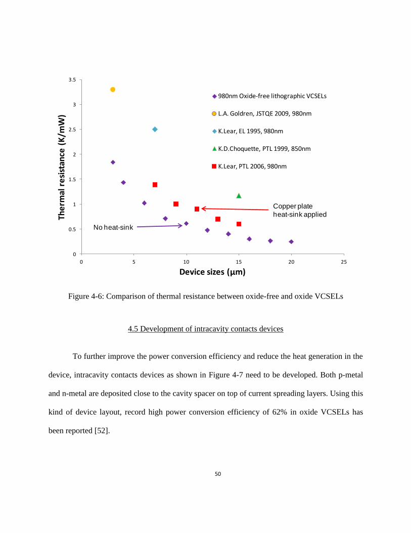
50
Copper plate
heat-sink applied
No heat-sink
0
0.5
1
1.5
2
2.5
3
3.5
0 5 10 15 20 25
The
rmal
re
sist
ance
(K
/mW
)
Device sizes (μm)
980nm Oxide-free lithographic VCSELs
L.A. Goldren, JSTQE 2009, 980nm
K.Lear, EL 1995, 980nm
K.D.Choquette, PTL 1999, 850nm
K.Lear, PTL 2006, 980nm
Figure 4-6: Comparison of thermal resistance between oxide-free and oxide VCSELs
4.5 Development of intracavity contacts devices
To further improve the power conversion efficiency and reduce the heat generation in the
device, intracavity contacts devices as shown in Figure 4-7 need to be developed. Both p-metal
and n-metal are deposited close to the cavity spacer on top of current spreading layers. Using this
kind of device layout, record high power conversion efficiency of 62% in oxide VCSELs has
been reported [52].

51
There are many advantages to make intracavity contacts devices in terms of reduce
device resistance and heat generation. Most Joule heating and free carrier absorption heating are
from the DBRs for VCSELs. The current pass is changed in this kind of device layout. There is
no current flow in the DBRs so that the device voltage as well as the resistive heating can be
reduced. Since there is no current flow in the DBRs, the DBRs can be undoped without grading
layers in it. In this case, the free carrier absorption loss in the DBRs will be reduced and the
reflectivity of the DBRs will be higher.
n+ GaAs substrate
P-metal
N-metal
Current
flow
Figure 4-7: Schematic of structure for intracavity contacts devices.
The process flow of oxide-free lithographic VCSELs can be modified as following to
make intracavity contacts devices as shown in Figure 4.8. After the regrowth of the p-side DBRs
with a GaAs current spreading layer designed in it, the structure is dry etched to the p-side
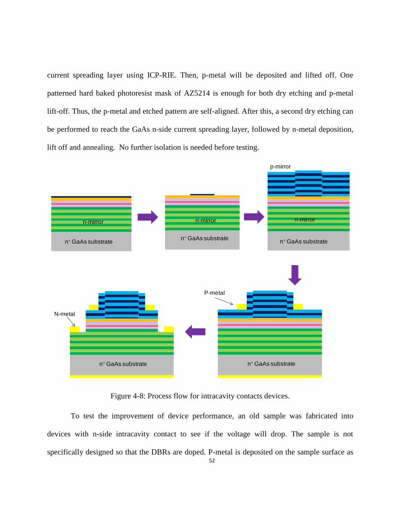
52
current spreading layer using ICP-RIE. Then, p-metal will be deposited and lifted off. One
patterned hard baked photoresist mask of AZ5214 is enough for both dry etching and p-metal
lift-off. Thus, the p-metal and etched pattern are self-aligned. After this, a second dry etching can
be performed to reach the GaAs n-side current spreading layer, followed by n-metal deposition,
lift off and annealing. No further isolation is needed before testing.
n+ GaAs substrate
n-mirror
n+ GaAs substrate
n-mirror
n+ GaAs substrate
n-mirror
p-mirror
P-metal
n+ GaAs substraten+ GaAs substrate
N-metal
Figure 4-8: Process flow for intracavity contacts devices.
To test the improvement of device performance, an old sample was fabricated into
devices with n-side intracavity contact to see if the voltage will drop. The sample is not
specifically designed so that the DBRs are doped. P-metal is deposited on the sample surface as

53
usual. However, the width of the metal ring round the mesas varies from 5μm to 10μm and 15μm
to test the influence of the p-metal ring size on the device lateral resistance. Figure 4-9 shows the
top view of the fabricated device with n-side intracavity contact on current spreading layer.
Figure 4-9: Top view of device with intracavity n-contact.
The measured characteristics of 6μm devices with intracavity n-contact are summarized
in table 4-2 and compared with the data from previous test on device with backside n-contact.
The devices are fabricated from the same wafer. The IV and LI curves are illustrated in Figure 4-
10. The measurement shows that the intracavity n-contact devices do have lower voltage
compared with the device with backside n-contact. However, the output power and power
conversion efficiency drop while the threshold current goes up for the intracavity n-contact
devices. This is because the current confinement of this oxide-free lithographic VCSEL is not as
strong as that of the oxide VCSELs. When intracavity contacts layout is used, the blocking
region is closer to the n-metal while the mesa is farer. Current tends to flow though the blocking
region resulting in larger leakage current. This can be further confirmed by the fact that device

54
with wider ring metal width has higher threshold current, lower output power and lower power
conversion efficiency.
To solve the leakage current problem in the intracavity contacts devices, further
optimization of cavity spacer and mesa need to be carried out to improve the current blocking. At
the same time, increase the doping level in the current spreading layer can be tried to help the
lateral injection of the current. More experiments need to be carried out to optimize the design
for intracavity contacts devices.
Table 4-2: Characteristics of 6μm devices with intracavity n-contact and backside n-contact
Ith (mA) P_max(mW) slope eff. wall-plug eff. Volt at 10kA/cm2
backside n contact 1.65 16.95 74.5% 39.5% 1.54
5 um metal width 1.64 13.79 63.5% 34.3% 1.5
10 um metal width 1.68 12.03 61.6% 29.6% 1.49
15 um metal width 2.15 11.05 52.1% 24.5% 1.47
1
1.25
1.5
1.75
2
2.25
2.5
2.75
0 10 20 30 40
Vo
ltag
e (V
)
Current (mA)
Intracavity contact, 5 um metal widthIntracavity contact, 10 um metal widthIntracavity contact, 15 um metal widthbackside n contact
0
2.5
5
7.5
10
12.5
15
17.5
0 10 20 30 40
Ou
tpu
t P
ow
er
(mw
)
Current (mA)
intracavity n contact, 5 um metal widthIntracavity n contact, 10 um metal widthintracavity n contact, 15 um metal widthBackside n contact
Figure 4-10: IV (left) and LI (right) curves of 6μm devices with intracavity n-contact and
backside n-contact

55
4.6 Summary
Oxide-free lithographic VCSELs are developed to solve the self-heating problem of
oxide VCSELs and improve the device performance. Optimization of the DBRs structures results
in low resistance and low free carrier absorption DBRs. Power conversion efficiency higher than
50% has been reached. Device performance is better than 980nm commercial oxide VCSEL in
terms of maximum output power and power conversion efficiency. Removing the oxide layer
and using AlAs/GaAs DBRs leads to lower thermal resistance and reliable performance in the
oxide-free lithographic VCSELs. Developing intracavity contacts devices will further reduce the
device voltage and heat generation in the DBRs due to both resistive heating and optical free
carrier absorption loss. Optimization of cavity spacer and mesa needs to be carried out to solve
the leakage current problem in the intracavity contacts device layout.

56
LIST OF REFERENCES
[1] J. Piprek, P. Abraham, and J. E. Bowers, “Self-consistent analysis of high-temperature effects on strained-
layer multiquantum-well In-GaAsP-InP lasers,” IEEE J. Quantum Electron., vol. 36, no. 3, pp.366-374,
Mar. 2000.
[2] C. Y. Tsai, L. F. Eastman, and Y. H. Lo, “Hot carrier and hot phonon effects on high-speed quantum well
lasers,” Appl. Phys. Lett., vol. 63, pp. 3408–3410, 1993.
[3] WC.NG, Y. Liu , and K. Hess, “Lattice Temperature Model and Temperature Effects in Oxide-Confined
VCSEL’s,” Journal of Computational Electronics,Volume 3, Issue 2, pp 103-116, 2004
[4] J. Piprek, J. K. White, and A. J. SpringThorpe, “What limits the maximum output power of long-
wavelength AlGaInAs–InP laserdiodes?,” IEEE J. Quantum Electron., vol. 38, no. 9, pp. 1253–1259,
Sep. 2002
[5] Y. Liu, W. C. Ng, K.D. Choquette, and K. Hess, “Numerical investigation of self-heating effects of oxide-
confined vertical-cavity surface-emitting lasers,” IEEE J. Quant. Electron. 41, 15 (2005).
[6] K. L. Lear, K.D. Choquette, R.P. Schneider Jr, S.P. Kilcoyne and K.M. Geib. "Selectively Oxidized
Vertical Cavity Surface Emitting Lasers with 50% Power Conversion Efficiency." Electronics Letters
31, no. 3 (1995): 208-209
[7] B. Etienne, J. Shah, R. F. Leheny, and R. E. Nahory, “Influence of hot carriers on the temperature
dependence of threshold in 1.3-_mInGaAsP lasers,” Appl. Phys. Lett., vol. 41, pp. 1018–1020, 1982.
[8] Jean-Francois Seurin ; Chuni L. Ghosh ; Viktor Khalfin ; Aleksandr Miglo ; Guoyang Xu ; James D.
Wynn ; Prachi Pradhan and L. Arthur D'Asaro, "High-power high-efficiency 2D VCSEL arrays", Proc.
SPIE 6908, Vertical-Cavity Surface-Emitting Lasers XII, 690808 , 2008
[9] Pikhtin, N. A., Slipchenko, S. O., Sokolova, Z. N., and Tarasov, I. S., "Internal Optical Loss in
Semiconductor Lasers," Semiconductor vol. 38, pp. 360-367, 2004.
[10] Garbuzov, D., Xu, L., Forrest, S. R., Menna, R., Martinelli, R., and Connolly, J. C., "1.5μm wavelength
SCH-MQW InGaAsP/InP broadened-waveguide laser diodes with low internal loss and high output
power," Electron. Lett., vol. 32, pp. 1717-1719, 1996.

57
[11] Slipchenko, S. O., Vinokurov, D. A., Pikhtin, N. A., Sokolova, Z. N., Stankevich, A. L., Tarasov, I. S.,
and Alferov, Z. I., "Ultralow internal optical loss in seperate-confinement quauntum well
heterostructures," Semiconductor, vol. 38, pp. 1430-1439, 2004.
[12] R. N. Hall, G. E. Fenner, J. D. Kingsley, T. J. Soltys, and R. O. Carlson, Phys. Rev. Lett. 9, 366 (1962).
The editor received this paper on Sept. 24, 1962.
[13] M. I. Nathan, W. P. Dumke, G. Burns, F. H. Dill,Jr., and G. Lasher, Appl. Phys. Lett. 1, 62 (1962). The
editor received this paper on Oct. 4, 1962.
[14] N. Holonyak, Jr. and S. F. Bevacqua, Appl. Phys. Lett. 1, 82 (1962). The editor received this paper on Oct.
17, 1962.
[15] T. M. Quist, R. H. Rediker, R. J. Keyes, W. E. Krag, B. Lax, A. L. McWhorter, and H. J. Zeiger, Appl.
Phys. Lett. 1, 91 (1962). The editor received this paper on Oct. 23, 1962 and in final form Nov. 5,
1962.
[16] Alferov, Zh. I., D. Z. Garbuzov, V. S. Grigor’ev, Yu. V. Zhilyaev, L. V. Kradinova, V. I. Korol’kov, E. P.
Morozov, O. A. Ninua, E. L. Portnoy, V. D. Prochukhan, and M. K. Trukan, 1967, ‘‘Injection
luminescence of epitaxial heterojunctions in the GaP-GaAs system,’’ Sov. Phys. Solid State 9, 208.
[17] Alferov, Z. I., Andreev, V. M., Garbuzov, D., and Zhilyaev, Y. V., "Investigation of the influence of the
AlAs-GaAs heterostructure parameters on the laser threshold current and realizaton of continuous
emission at room temperature " Sov. Phys.Semiconductor, vol. 4, p. 1573, 1970.
[18] J. P. van der Ziel, R. Dingle, R. C. Miller, W. Wiegmann, and W. A. Nordland Jr., Appl. Phys. Lett.
26,463 (1975)
[19] Dupuis, R. D., P. D. Dapkus, N. Holonyak, Jr., E. A. Rezek, and R. Chin, 1978, ‘‘Room temperature
operation of quantum-well Ga12xAlxAs-GaAs laser diodes grown by metalorganic chemical vapor
deposition,’’ Appl. Phys. Lett. 32, 295.
[20] Tsang, W. T., 1982, ‘‘Extremely low threshold (AlGa)As graded-index waveguide separate-confinement
heterostructure lasers grown by molecular-beam epitaxy,’’ Appl. Phys. Lett. 40, 217.
[21] Alferov, Z. I., Vasiliev, A. M., and Ivanov, S. V., "Reducing of the threshold current in GaAs-AlGaAs
DHS SCH quantum well restriction by short period superlattice of variable period," Sov. Tech. Phys.
Lett., vol. 14, p. 782, 1988.

58
[22] N. Kirstaedter, N.N. Ledentsov, M. Grundmann, D. Bimberg, V.M. Ustinov, S.S. Ruvimov, M.V.
Maximov, P.S. Kop’ev, Zh.1. Alferov, U. Richter, P. Werner, U. Gdsele and J. Heydenreich, Electron.
Lett. 30, 1416 (1994)
[23] Liu, G. T., Li, H., Malloy, J., and Lester, L. F., "Extremely low room-temperature threshold current
density diode lasers using InAs dots in In0.15Ga0.85As quantum well," Electron. Lett., vol. 35, pp.
1163-1164, 1999.
[24] Park, G., Schekin, O. B., Huffaker, D. L., and Deppe, D. G., "1.3-μm quantum-dot laser," IEEE Photonics
Technol. Lett., vol. 12, pp. 230-232, 2000.
[25] Seller, I. R., Liu, H. Y., Groom, K. M., Childs, D. T., Robbins, D., Badcock, T. J., Hopskinson, M.,
Mowbray, D. J., and Skolnick, M. S., "1.3μm InAs/GaAs multilayer quantum-dot laser with extremely
low room-temperature threshold current density " Electron. Lett., vol. 40, pp. 1412-1413, 2004.
[26] Freisem, S., Ozgur, G., Shavritranuruk, K., Chen, H., and Deppe, D.G.: “Very low threshold current
density continuous wave quantum dot laser,” Electron. Lett., 2008, 44, pp. 679–680
[27] D.G. Deppe, K. Shavritranuruk, G. Ozgur, H. Chen and S. Freisem, “Quantum dot laser diode with low
threshold and low internal loss,” Electron. Lett. 45, 54 (2009)
[28] A.N.AL-Omari, G.P.Carey, S.Hallstein, J.P.Watson, G.Dang and K.Lear, “Low Thermal resistance High-
Speed Top-Emitting 980-nm VCSELs,” IEEE Photon. Technol. Lett. 18, 1225-1227 (2006).
[29] Teo Jin Wah Ronnie. Advances in High-Power Laser Diode Packaging, Semiconductor Laser Diode
Technology and Applications, Dr. Dnyaneshwar Shaligram Patil (Ed.), ISBN: 978-953-51-0549-7,
InTech, 2012
[30] Lee, H.K., Song, Y.M., Lee, Y.T., and Yu, J.S.: ‘Thermal analysis of asymmetric intracavity-contacted
oxide-aperture VCSELs for efficient heat dissipation’, Solid-State Electron., 53, pp. 1086–1091, 2009
[31] Quagan, R., "Laser Diode Heat Spreaders," Ion Beam Milling, Inc.
[32] B. Sumpf, S. Deubert, G. Erbert, J. Fricke, J.P. Reithmaier, A. Forchel, R. Staske and G. Trankle, “High-
power 980nm quantum dot broad area lasers”, Electron. Lett., 39, pp. 1655–1657 ( 2003)
[33] F. Klopf, J.P. Reithmaier, A. Forchel, P. Collot, M. Krakowski and M. Calligaro, “High performance 980
nm quantum dot lasers for high power applications”, Electron. Lett., 37, pp. 353–354 (2001)

59
[34] Zhangcheng Xu, “Sub-monolayer Deposited InGaAs/GaAs Quantum Dot Heterostructures and Lasers,”
PhD Thesis, Technical University of Denmark, 2004
[35] K.Iga, “Vertical-Cavity Surface-Emitting Laser: Its Conception and Evolution,” Jpn. J.Appl. Phys., Vol.
47, No. 1, pp.1-10, 2008.
[36] H. Soda, K. Iga, C. Kitahara, and Y. Suematsu, “GaInAsP/InP surface emitting injection lasers,” Jpn. J.
Appl. Phys., vol. 18, No. 12, pp. 2329–2330, 1979.
[37] K. Iga, S. Ishikawa, S. Ohkouchi, T. Nishimura, “Room-temperature pulsed oscillation of GaAlAs/GaAs
surface emitting injection laser,” Appl. Phys. Lett. 45, pp. 348, 1984
[38] F. Koyama, S. Kinoshita, and K. Iga, “Room-temperature continuous wave lasing characteristics of GaAs
vertical cavity surface-emitting laser,” Appl. Phys. Lett., 55, no. 3, pp. 221–222, 1989.
[39] P.L. Gourley and T.j. Drummond, “Visible, room-temperature, surface-emitting laser using an epitaxial
Fabry–Perot resonator with AlGaAs/AlAs quarter-wave high reflectors and AlGaAs/GaAs multiple
quantum wells,” Appl. Phys. Lett. 50, pp. 1225, 1987
[40] T. Sakaguchi, F.Koyama, and K. Iga, “Vertical cavity surface-emitting laser with an AlGaAs/GaAs Bragg
Reflector,” Electron. Lett. 24, 928 (1988).
[41] J. L. Jewell, A. Scherer, S.L. Mccall et al., “Low-threshold electrically pumped vertical-cavity surface-
emitting microlasers,” Electron. Lett. 25, 1123 (1989).
[42] Lee, Y.H.; Jewell, J.L.; Tell, B.; Brown-Goebeler, K.F.; Scherer, A.; Harbison, J.P.; Florez, L.T.; “Effects
of etch depth and ion implantation on surface emitting microlasers”, Electron. Lett. 26, 225-227
(1990).
[43] B.J. Thibeault, T.A. Strand, T. Wipiejewski, M.G. Peters, D.B. Young, S.W. Corzine, L.A. Coldren, and
J.W. Scott, "Evaluating the effects of optical and carrier losses in etched-post vertical cavity lasers," J.
Appl. Phys., 78, 5871-5875, (1995).
[44] M. G. Peters, D. B. Young, F. H. Peters, J. W. Scott, B. J. Thibeault, and L. A. Coldren, “17.3% Peak
Wall Plug Efficiency Vertical-CavitySurface-Emitting Lasers Using Lower Barrier Mirrors,” IEEE
Phtonics Technology Letters, vol. 6, pp. 31-33, Jan. 1994.
[45] K. Tai, R.J. Fischer, K.W.Wang, S.N.G. Chu, and A.Y. Cho, “Use of implant isolation for fabrication of
vertical cavity surface-emitting laser diodes,” Electron. Lett. 25, 1644-1645 (1989).

60
[46] R.A. Morgan, M.K. Hibbs-Brenner, R.A. Walterson, J.A. Lehman, et al, “Producible GaAs-based
MOVPE-grown vertical-cavity top-surface emitting lasers with record performance,” Electron. Lett.
31, 462-464 (1995).
[47] D. L. Huffaker, D. G. Deppe, K. Kumar, and T. J. Rogers, “Native-oxide defined ring contact for low
threshold vertical-cavity lasers,” Appl. Phys. Lett. 65, 97 (1994);
[48] K.D. Choquette, R.P. Schneider, Jr., K.L. Lear and K.M. Geib, “Low threshold voltage vertical-cavity
lasers fabricated by selective oxidation,” Electron. Lett. 30, 2043-2044 (1994).
[49] J. M. Dallesasse, N. Holonyak, Jr., A. R. Sugg. T A. Richard, and N. El-Zein, “Hydrolyzation oxidation of
AlxGa1−xAs-AlAs-GaAs quantum well heterostructures and superlattices,”Appl. Phys. Lett. 57, 2844
(1990).
[50] G.M. Yang, M.H. MacDougal and P.D. Dapkus, “Ultralow threshold current vertical-cavity surface-
emitting lasers obtained with selective oxidation,” Electron. Lett. 31, 886-888 (1995).
[51] B. Weigl, M. Grabherr, C. Jung, R. Jager, G. Reiner, R. Michalzik, D. Sowada, K.J. Ebeling, “High-
Performance Oxide-Confined GaAS VCSEL’s,” IEEE J. of Selected Topics in Quantum Electronics,
vol. 3, 2, 409-415,(1997).
[52] K. Takaki, N. Iwai, K. Hiraiwa, S. Imai, H. Shimuzu, T. Kageyama, Y. Kawakita, N. Tsukiji, A.
Kasukawa, “A recorded 62% PCE and low series and thermal resistance VCSEL with a double intra-
cavity structure,” 21st International Semiconductor Laser Conference, PDP1, (2008)
[53] Fei Tan, Mong-Kai Wu, Michael Liu, Milton Feng and Nick Holonyak, “850 nm Oxide-VCSEL With
Low Relative Intensity Noise and 40 Gb/s Error Free Data Transmission,” IEEE Photon. Technol.
Lett., pages 289 – 292, vol. 26, 3, (2014)
[54] S. Guha, F. Agahi, B. Pezeshki, J.A. Kash, D.W. Kisker, and N.A. Bojarczuk, “Microstructure of
AlGaAs-oxide heterolayers formed by wet oxidation,” Appl. Phys. Lett., 68, pp. 906-908, 1996
[55] K. L. Lear et al., “Small and large signal modulation of 850 nm oxide confined vertical- cavity surface-
emitting lasers,” Advances in Vertical Cavity Surface Emitting Lasers in Trends in Optics and
Photonics Series, 1997, vol. 15, pp. 69–74.
[56] D. Lu, J. Ahn, H. Huang and D. G. Deppe, “All-epitaxial mode-confined vertical-cavity surface-emitting
laser,” Appl.Phys.Lett. 85, pp. 2169-2171 (2004).
61
[57] S. Adachi, “Lattice thermal resistivity of III-V compound alloys,” J. Appl. Phys., vol. 54, no. 4, pp.
1844-1848, 1983.
[58] X. Yang, G. Zhao, M. Li, X. Liu, Y. Zhang, and D.Deppe, “ 50% Power Conversion Efficiency on a Non-
Oxide VCSEL”, CLEO: Science and Innovations: Optical Society of America (2014).
[59] “Vertical-Cavity Surface-Emitting Laser Technology”, www.princetonoptronics.com
[60] G. Zhao, X. Yang, Y. Zhang, M. Li, D.G. Deppe, C. Cao, J. Thorp, P. Thiagarajan and M. McElhinnery.
"Record Low Thermal Resistance of Mode-Confined VCSELs Using AlAs/AlGaAs DBRs." CLEO:
Science and Innovations: Optical Society of America (2013).
[61] Chang, Yu-Chia and Larry A. Coldren. "Efficient, High-Data-Rate, Tapered Oxide-Aperture Vertical-
Cavity Surface-Emitting Lasers." Selected Topics in Quantum Electronics, IEEE Journal of 15, no. 3
(2009): 704-715.
[62] R. Pu, C.W. Wilmsen, K.M. Geib and K.D. Choquette. "Thermal resistance of VCSELs bonded to
integrated circuits", IEEE Photonics Technology Letters,Volume.11, Issue.12, pp.1554, 1999
[63] G.Zhao, A. Demir, S. Freisem, Y. Zhang, X. Liu and D. G. Deppe, “New VCSEL technology with
scalability for single mode operation and densely integrated arrays”, Proc. SPIE 8054, 80540A .2011