semiconduct or spintr onics f or q u antum...
TRANSCRIPT

SEMICONDUCTOR SPINTRONICS FOR QUANTUM COMPUTATION
MICHAEL E. FLATTE (michael [email protected])Optical Science and Technology Center,Department of Physics and Astronomy, andDepartment of Electrical and Computer Engineering,University of Iowa, Iowa City, IA 52242, USA
Abstract: Encoding quantum information in spins embedded in semiconductors (electronic, ionic,or nuclear) o!ers several potential approaches towards solid-state quantum computation. Electronicspin transport, persistence and manipulation in nonmagnetic semiconductor materials, as well asthe interaction of electronic spins with optics, are the fundamental properties reviewed here. Thepresentation focuses on the material properties important for implementing quantum computation,and on the characteristics that may lead more rapidly to scalable solutions for quantum informationprocessing.
Keywords: spin coherence, spin dynamics, quantum computation, spin transport
1 Introduction
The range of proposed quantum-mechanical systems that can implement quantumcomputational algorithms continues to grow, and progress towards functional scal-able devices appears rapid. An agreed set of criteria for such systems (Bennett andDiVincenzo, 2000) includes the initialization, evolution, and measurement of aset of entities that can be approximated as two-level systems (qubits). A universalquantum computer would have a selectable number of these qubits and a pro-grammable arrangement of quantum gates (referred to as a quantum algorithm).An important distinction should be understood at the beginning between physi-cal qubits and logical qubits. Physical qubits are elementary two-state systems,but information encoded simply in single physical qubits is highly susceptible todecoherence. Quantum error correction is possible if multiple physical qubits areused to encode a single logical, or coded, qubit (Preskill, 1998). The entangle-ment between the physical qubits that constitute a logical qubit permits a formof redundancy, and thus error correction, even though quantum information itselfcannot be copied completely from one qubit to another. In order to implement anyquantum algorithm it is su"cient to perform one-qubit and two-qubit operationson the logical qubits (Barenco et al., 1995).
1M.E. Flatte and I. Tifrea (eds.), Manipulating Quantum Coherence in Solid State Systems, 1–52.c! 2007 Springer.

2 SEMICONDUCTOR SPINTRONICS FOR QUANTUM COMPUTATION
A concrete realization of a solid-state quantum computation structure basedon electron spins confined within quantum dots was proposed by Loss andDiVincenzo (1998). The single qubit operations could be implemented withlocal AC fields or by controlling the resonance frequencies of individual qubits.Two-qubit operations could be implemented by controlling the exchange interac-tion between two quantum dots with electric gates, and spin detection could beachieved through ferromagnetic nucleation. A similar proposal relying on nuclearspin qubits of donors in silicon appeared roughly simultaneously (Kane, 1998).Subsequent work has shown that in a solid-state environment with spins as logicalqubits both one-qubit and two-qubit operations may require only one type ofphysical gate interaction, such as the exchange interaction (DiVincenzo et al.,2000; Levy, 2002; Petta et al., 2005). Reviews of these experimental pathwaystowards spin manipulation in quantum dots include Kouwenhoven et al. (2001)and Hanson et al. (2006).
The material presented here considers topics that may contribute to the imple-mentation of quantum computation in solid-state spin-based systems in the future.Spin transport, the topic of section 2, and spin decoherence in electron spin ensem-bles, the topic of section 3, may play important roles in the e"cient initializationof large arrays of spin-based qubits. The following section 4, on the electrical con-trol of ionic spins in a semiconductor, shows quantum manipulation of ionic spinscan be achieved without the use of any magnetic fields. The subsequent section 5explores the spin-based properties of quantum dots, and the interaction of thesespins with photons. Optical techniques can be used to probe the spin orientationand to manipulate the spins themselves. Section 6 describes a method for couplingquantum dot spins to individual photons within a microcavity (and the applicationof this method to teleportation). Section 7 presents some conclusions and topicsfor further development.
2 Spin-Dependent Processes in Electrical Transport
Initialization of multiple qubits within a quantum computer may require the trans-port of highly spin-polarized distributions across a material, followed by insertionof individual spins into localized regions such as quantum dots, or transfer ofthe spin information from the moving distribution to a set of localized spins.The applications of spin transport, however, also extend to a variety of possibleinformation processing devices such as spin transistors (Datta and Das, 1990).The treatment presented here would also apply to the transport of spin polarizeddistributions in such systems.
The development of theories of spin transport initially followed in the foot-steps of the broad and mature field of charge transport, by attempting to correlatephysical regimes of spin transport with corresponding regimes of charge transport.

SEMICONDUCTOR SPINTRONICS FOR QUANTUM COMPUTATION 3
As the field of spin transport has become more mature the analogies have been fur-ther refined. A very helpful analogy has been to correlate the “two-channel” modelfor spin flow, which only tracks the spin polarization along a fixed quantizationaxis, with the two-band model for carrier flow in a semiconductor. Phenomenasuch as local charge neutrality and drift, which have been thoroughly explored forthe two-band model for carrier flow in a semiconductor, can be transposed almostentirely to the transport of spin within the two-channel model. Most recently, withthe treatment of many-body e!ects in spin-dependent transport, new regimes withno natural analogs in charge transport have been identified (Qi et al., 2006).
2.1 REGIMES OF CHARGE CURRENT FLOW
The most general description of the current associated with charge carriers wouldinclude the response of the full many-particle wave function to an applied electricfield. A number of approximate schemes have been introduced to describe currentflow with only a few parameters. Tremendous simplification, for example, can beachieved through the introduction of a local chemical potential. The key assump-tion behind this approximation is that the carriers in a particular spatial region arein equilibrium with other carriers in that region, but may be out of equilibriumwith carriers elsewhere in the material. This assumption can be justified when themean free path of carriers is shorter than the typical length scale of the regionthrough which the carriers are traveling. In these circumstances, for carriers asso-ciated with a single band (and ignoring spin), the spatially-dependent distributionof the carriers can be summarized with two parameters: the local chemical poten-tial !µ(r) measured relative to the electric potential, and the electric potential "(r).Note that in this treatment the units of these two quantities are Volts.
The current J can be then related directly to the local change in the totalchemical potential !µ " ",
J = ##(!µ " "), (1)
where # is the conductivity. In principle the conductivity depends on !µ andthus must be found self-consistently. In semiconductors, which can sustain largedeviations of the local charge density from equilibrium, it is convenient to separatethe conductivity into the carrier density and mobility, as the mobility depends lesssensitively on !µ than the carrier density.
Conservation of charge requires that in steady-state transport every electronpassing in to an element of a circuit must pass out, and thus
# · J = 0. (2)
Solution of Eqs. (1) and (2) for the boundary conditions appropriate for a givenvoltage drop, along with a self-consistent solution for the conductivity, and

4 SEMICONDUCTOR SPINTRONICS FOR QUANTUM COMPUTATION
a self-consistent solution of the Poisson equation relating the electric field to thelocal variation of the charge density,
# · E = "e!
(n " no), (3)
will produce a full description of the current distribution in response to an appliedvoltage. In Eq. (3) n is the carrier density, no is the equilibrium carrier density, Eis the electric field, e is the magnitude of the electric charge, and ! is the dielectricconstant.
In lightly-doped semiconductors drift–di!usion equations are more com-monly used than Eqs. (1)–(3). The drift–di!usion equations, however, are veryclosely related (Kittel and Kroemer, 1980), as illustrated here. Equation (2)permits the current to be written as the gradient of a scalar potential, J = #$,which can be written as Eq. (1). For nondegenerate carriers !µ = kBT ln(n/no),and Eq. (1) can be written as
J = #E + (#kT/n)#n = #E + eD#n, (4)
where kB is Boltzmann’s constant, T is the temperature, and D is the di!usionconstant. The far right expression of Eq. (4) also holds in the degenerate regimeif n/no $ 1. Thus one can use either the chemical potential expression or thedrift–di!usion equations to calculate the current in a general situation.
The choice of using the quasichemical potential equations or the drift di!usionequations is made solely on convenience. Frequently quasichemical potentials areused when the carrier density is su"ciently high that the conductivity can be con-sidered independent of the nonequilibrium spin-polarized carriers (as is the casein metals). Under these conditions Eq. (1) can be solved for the quasichemicalpotential with the appropriate boundary conditions (continuity of current, anda given voltage drop across the structure) and it is not necessary to considerthe carrier density as a separate variable to be determined self-conistently. Whenthe carrier density is low enough that a small change in carrier density markedlychanges the conductivity of the material (as can be the case in semiconductors)then # in Eq. (1) must be determined self-consistently, requiring solving for thecarrier density in addition to the chemical potential and the electric field. In thesesituations it is easier to use drift–di!usion equations, which can be written withoutthe chemical potential as a separate quantity to be determined.
In a set of regimes often termed “ballistic transport” the mean free path of car-riers is longer than the typical length scale of the region through which the carriersare traveling, and the occupation of each state of band index j and momentum kmust be provided. In a further set of regimes often termed “mesoscopic transport”,the phase relationship between states of di!ering j and/or k remains importantduring transport, and spatial interference between waves of di!ering k is observed.One realization of this is the reorganization of carrier eigenstates from momen-tum states (which are no longer eigenstates) into new wave functions that are

SEMICONDUCTOR SPINTRONICS FOR QUANTUM COMPUTATION 5
coherent superpositions of di!erent momentum states in one or more directions.For example, eigenstates of quantum wells are constructed from counterpropagat-ing momentum states in the direction of carrier confinement. Many definitions ofthe terms ballistic and mesoscopic transport are used in the literature, so some willdi!er from those introduced above.
2.2 HOW DOES A SPIN CURRENT FLOW?
Spin currents can flow in magnetic and nonmagnetic materials, parallel to or per-pendicular to an applied electric field, or even in the absence of a static appliedelectric field. A brief survey of spin current mechanisms will provide an introduc-tion to the range of spin transport phenomena already demonstrated in solid-statematerials.
One simple configuration for spin-current flow involves an applied electricfield and a spin current flowing parallel to that field. This occurs naturally inmagnetic materials due to the di!ering conductivity for spin-up and spin-downcarriers. In the nondegenerate limit the conductivity would be
#%(&) = n%(&)eµ%(&), (5)
and in the degenerate limit it would be
#%(&) = N%(&)(EF,%(&))e2D%(&), (6)
where the quantities introduced in section 2.1 have now been distinguished byspin direction (up or down). Shown in Figure 1a is an example of a spin-splitelectronic structure, as might be found in a magnetic material, with a di!erentdensity of spin-up and spin-down carriers, as well as a di!erent density of statesfor spin-up and spin-down carriers. It is likely in this situation that the di!usion
(a) magnetic materials
Fermienergy
(b) nonmagnetic materials
Fermienergy
Fermienergy
spin injection
Figure 1. (a) Spin-split electronic structure, such as for a magnetic material. (b) Spin-degenerateelectronic structure for a nonmagnetic material, but with additional nonequilibrium spin-polarizedcarriers that modify the conductivity and render it spin-dependent

6 SEMICONDUCTOR SPINTRONICS FOR QUANTUM COMPUTATION
constant for spin-up and spin-down carriers would also di!er. Whether the degen-erate or nondegenerate forms of the conductivity are appropriate, the conductivityof the two spin orientations will be di!erent. In Figure 1a there is no spin-splittingof the chemical potential, so EF,% = EF,&. If the spin-resolved conductivites arespatially uniform this condition is preserved for the spatially-dependent spin-upand spin-down chemical potentials,
"%(r) = "&(r). (7)
Once the conductivities vary spatially these chemical potentials may di!er, andthe chemical potentials and current flow for spin-up and spin-down carriers canbe found independently within the two-channel model (Mott, 1936; Fert andCampbell, 1968).
In Figure 1b, by contrast, a nonmagnetic material is shown, but the chem-ical potential for spin-up carriers di!ers from that for spin-down carriers. Thisphenomenon, commonly referred to as “spin injection” can occur through theoptical generation of spin-polarized carriers (Meier and Zachachrenya, 1984) (asdescribed in section 2.5 and Chapter 4) or through flowing a current from a mag-netic material through a nonmagnetic material (Aronov and Pikus, 1976; Johnsonand Silsbee, 1988). Once the nonequilibrium density of spins has been generated,both the density of carriers and their density of states (and thus their conductiv-ities) will depend on the carriers’ spin direction, and a spin current will flow inresponse to an applied electric field.
Another method of generating spin currents does not require an applied elec-tric field, for it consists of optically generating a distribution of nonequilibriumcarriers in which the spin-up carriers are moving in an opposite direction to thespin-down carriers, as shown in Figure 2. This can be performed by interferingtwo polarized optical pulses of di!ering photon energy in a semiconductor (Bhatand Sipe, 2000) and has been demonstrated in GaAs quantum wells (Stevens et al.,2003) and bulk ZnSe (Hubner et al., 2003). The current survives until scattering
Fermienergy
Fermienergy
right-moving electronsleft-moving electrons
Figure 2. Electron distributions corresponding to the flow of ballistic spin current. An accumula-tion of spin-down left-moving electrons and spin-up right-moving electrons yields a spin current,even though overall there is no density di!erence between spin-up and spin-down carriers

SEMICONDUCTOR SPINTRONICS FOR QUANTUM COMPUTATION 7
right-moving electrons left-moving electrons
Fermienergy
Fermienergy
Figure 3. The spin–orbit interaction alters the density of states of spin-up and spin-down carriersaccording to whether the spin is parallel or antiparallel to the carrier momentum. When a currentflows this produces a larger density of carriers of one spin than the other
of the ballistically-moving carriers eliminates the nonequilibrium distribution thatproduces the current.
Even without spin-selective di!erences in the occupation functions it is pos-sible to generate a spin current. The presence of spin–orbit interaction in solidsproduces a di!erent electronic structure for spin-up and spin-down carriers of thesame momentum. Time-reversal invariance, however, will force
E%(k) = E&("k), (8)
where E%(&)(k) is the energy of the spin-up (spin-down) carrier of momentum k.A schematic spin–orbit correlated electronic structure is shown in Figure 3. Whena di!usive charge current flows there are more carriers moving in the direction ofthe current than in the opposite direction, and as a result a greater occupation forone spin direction than the other (Edelstein, 1990).
Still other phenomena can produce spin currents. In the spin Hall e!ect(described in detail in Chapters 2 and 4) the flow of charge current in one directionyields a transverse spin current through asymmetries in the band structure or inthe scattering of carriers from impurities.
2.3 PROCESSES MODIFYING SPIN MOTION IN SEMICONDUCTORS
Two principal characteristics modify spin current once it has started to flow. Thefirst is the influence of internal magnetic fields and spin decoherence on the spinmotion. In a magnetic material the internal fields are present at all times, andin a nonmagnetic material with inversion asymmetry such magnetic fields alsoexist once carriers begin to move. In a nonmagnetic material these magnetic fieldsoriginate from the electric fields of the crystal structure itself, relativistically trans-formed into the rest frame of the carrier. For a nonmagnetic inversion symmetricmaterial these fields vanish, for inversion symmetry
E%(&)(k) = E%(&)("k) (9)

8 SEMICONDUCTOR SPINTRONICS FOR QUANTUM COMPUTATION
along with time-reversal symmetry, Eq. (8), produces degenerate eigenstates forthe two spin directions,
E%(k) = E&(k). (10)
As described in section 3 these internal magnetic fields provide the dominant con-tribution to spin relaxation and decoherence in nonmagnetic inversion-asymmetricsemiconductors.
The second important e!ect on spin transport is the role of the charges asso-ciated with the moving spins. It should not be a surprise that charge interactionsand spin properties are coupled to produce unexpected phenomena in transport,as magnetism in the solid state almost exclusively originates from the interplaybetween the Pauli exclusion principle and the Coulomb interaction itself.
2.4 MOTION OF SPIN DENSITY PACKETS IN SMALL ELECTRIC FIELDS
The transport of spin density packets in a semiconductor under conditions of smallelectric fields is closely related to the transport of charge polarization packets insemiconductors. So to begin consider the motion of a charge polarization packet ina semiconductor. This charge polarization packet corresponds to a nonequilibriumdensity of electrons n and/or holes p in a material with an equilibrium density ofelectrons no and holes po.
The current in such a two-band semiconductor is divided into an electroncurrent and a hole current,
je = neµeE + eDe#n = #eE + eDe#n, (11)jh = peµhE " eDh#p = #hE " eDh#p, (12)
which must satisfy the continuity equations
" e%n%t= "# · je " eG + eRnp, (13)
e%p%t= "# · jh + eG " eRnp, (14)
and the Poisson equation relating the local deviation from equilibrium of thecharge densities to the electric field,
# · E = "e!
(#n " #p). (15)
Here #n = n " no and #p = p " po, G is the generation rate for electron–holepairs, R is their recombination rate and ! is the dielectric constant.
Substituting the electron and hole currents into the continuity equations,neglecting the generation rate, assuming steady-state, and defining
Rnp = n/&e = p/&p, (16)

SEMICONDUCTOR SPINTRONICS FOR QUANTUM COMPUTATION 9
yields
De#2n " nµe# · E + µe#n · E = n&e, (17)
Dh#2 p + pµh# · E " µh#p · E = p&h. (18)
The middle term on the left-hand side will force the excess electrons and excessholes to move as a single packet, as #·E is proportional to the deviation from localcharge neutrality. A consistent solution to these two equations would not be foundsimply by setting #n = #p, however, for the di!usion constants and mobilities ofthe electrons and holes di!er.
The physics of this situation is shown in Figure 4. The applied electric fieldwill attempt to pull the electrons and holes in di!erent directions, but that motionwill generate a nonvanishing #n " #p, and thus an electric field that pulls the twocarriers together. This space-charge field is shown in Figure 4. The response ofthe carriers to this field depends on the carrier mobility. The high-conductivitycarriers will move more rapidly towards the low-conductivity carriers. To producea single equation for the motion of the electrons and holes, without requiring#n = #p, multiply Eq. (17) by #h, Eq. (18) by #e, and then add them together.This eliminates the self-consistent electric field without requiring local chargeneutrality, and produces
#hDe#2n + #eDh#2 p + #hµe#n · E " #eµh#p · E = #hn&e+ #e
p&h. (19)
Now the equation of motion of the packet can be found by allowing #n = #p.This approach allows us to work under conditions of approximate local charge
Electric Field
n(x)
p(x)
Space charge field
Charge density (p-n)
x x x
(a) (b) (c)
Figure 4. Motion of a charge polarization packet in an applied electric field. The electrons andholes wish to move in opposite directions, but the space-charge field pulls them together. Thecarriers with higher conductivity move towards those with lower conductivity, so the mobility anddi!usion of the packet is determined by the minority carriers

10 SEMICONDUCTOR SPINTRONICS FOR QUANTUM COMPUTATION
neutrality without (incorrectly) ignoring all aspects of the space-charge field.The resulting charge polarization packet, with excess electrons and excessholes moving together, is characterized by an ambipolar di!usion constant andambipolar mobility,
Dambi#2n + µambi#n · E = #n&r. (20)
where
Dambi =#hDe + #eDh
#h + #e, µambi =
#hµe " #eµh
#h + #e, &r = &e = &h. (21)
The last equation in Eq. (21) also uses detailed balance to determine &e = &h. In thelimit #e ' #h, Dambi ( Dh and µambi ( µh. This general result that the di!usionand mobility of the packet is dominated by the lower-conductivity species was thebasis of the Shockley–Haynes measurement of the mobility and di!usion constantof minority carriers in germanium (Haynes and Shockley, 1951).
The same approach can be used to determine the mobility and di!usionconstants of spin packets in semiconductors (Flatte and Byers, 2000), whichexplained some puzzling experimental results on the mobility of spin packetsin GaAs (Kikkawa and Awschalom, 1999). To describe spin packets, distinctcurrents and densities for spin-up and spin-down carriers, for both electronsand holes, must be introduced. Drift–di!usion equations for carrier motion in asemiconductor describe the combined motion of spin-up and spin-down electronsand holes in the presence of electric and quasi-electric fields, including the e!ectsof space charge fields on carrier motion (Awschalom et al., 2002). To includethe possibility of spin imbalance in both the conduction and valence bands, fourcurrents are required:
je% = en%µe%E + eDe%#n%, (22)je& = en&µe&E + eDe&#n&, (23)jh% = ep%µh%E " eDh%#p%, (24)jh& = ep&µh&E " eDh&#p&. (25)
The evolution in time and space of these four currents and the electric field comesfrom the four continuity equations,
" e%n%%t= "# · je% " e
n&&e&%+ e
n%&e%&
" eGe% + eR%&n%p& + eR%%n%p%, (26)
"e%n&%t= "# · je& + e
n&&e&%
" en%&e%&
" eGe& + eR&%n&p% + eR&&n&p&, (27)
e%p%%t= "# · jh% + e
p&&h&%
" ep%&h%&+ eGh% " eR&%n&p% " eR%%n%p%, (28)
e%p&%t= "# · jh& " e
p&&h&%+ e
p%&h%&+ eGh& " eR%&n%p& " eR&&n&p&, (29)

SEMICONDUCTOR SPINTRONICS FOR QUANTUM COMPUTATION 11
and the Poisson equation relating the local deviation from equilibrium of thecharge densities to the electric field,
# · E = "e!
(#n% + #n& " #p% " #p&). (30)
Here &"1ess) and &"1
hss) are rates for spin relaxation of electrons and holes respectivelyfrom spin s to spin s), Gns are generation rates for carrier n and spin s, Rss) are theelectron–hole pair recombination rates for an electron of spin s and hole of spins), and ! is the dielectric constant. If the hole spins are unpolarized then Eqs. (28)and (29) can be replaced by a single one with p% = p& = p/2.
Under conditions of approximate local charge neutrality often these equa-tions can be combined into a single one for a packet type with significant spinpolarization, following the procedure used for the charge polarization packets.Shown in Figure 5 are such packets for a semiconductor lacking backgrounddoping. For the hole spin packet and electron spin packet the derivation followsthrough exactly as before for the charge polarization packet, but either the holesor the electrons are entirely spin polarized. The lifetime of the hole spin packet,however, is much shorter than of the charge polarization packet, for the hole spinlifetime is typically much shorter than the charge recombination lifetime (Meierand Zachachrenya, 1984; Uenoyama and Sham, 1990). Thus the hole spin packetdecays into the charge polarization packet. The electron spin lifetime can be muchlonger than the charge recombination time, so in that regime the electron spinpacket decays by electron–hole recombination. If the hole spin lifetime were verylong, and recombination were 100% spin selective, then eventually the recom-bination of the electron spin packet might stop, but the short hole spin lifetimeguarantees that any spin imbalance in the hole population generated during a
Position
n
n
p
p
Electron spin packet
Position
Charge packet
Position
Hole spin packet
Figure 5. The packets of carriers possible in an undoped semiconductor require equal numbers ofelectrons and holes to maintain local charge neutrality. Thus packets of spin-polarized electrons (orholes) require a background of holes (or electrons)

12 SEMICONDUCTOR SPINTRONICS FOR QUANTUM COMPUTATION
(a) Charge packet(doped)
(b) Spin packet(undoped)
Position Position
n
n
pp
(c) Spin packet(doped)
Position
Figure 6. In the presence of a background of unpolarized electrons it is possible to satisfy localcharge neutrality by removing opposite-spin-oriented electrons when adding spin-polarized elec-trons. Thus the mobility and di!usion of this packet is determined by the properties of the electrons,not the minority holes
spin-selective recombination process with spin-polarized electrons would decayaway rapidly. Thus the lifetime of the electron spin packet is e!ectively the chargerecombination time.
The situation changes considerably when the semiconductor has a backgrounddoping of carriers. As shown in Figure 6 it is now possible to maintain localcharge neutrality by removing carriers from the background doping rather thanadding carriers of the other species. Thus additional spin-up electrons can be com-pensated for by removing spin-down electrons. No holes are required. The twoequations that play comparable roles in this case to Eqs. (13) and (14) are the twospin-resolved equations for the electrons, Eqs. (26) and (27), with p% = p& = 0.
The lifetime of the hole spin packet remains limited by the hole spin life-time, but the lifetime of the electron spin packet is no longer limited by thecarrier recombination lifetime. As holes no longer play a role in the decay of thepacket, the lifetime of the electron spin packet is determined by the electron spinlifetime. Thus an electron spin packet in an n-doped semiconductor can persist fortimes orders of magnitude longer than for an electron spin packet in an undopedsemiconductor, as seen in experimental observations in several semiconductormaterials (Kikkawa et al., 1997; Kikkawa and Awschalom, 1998). Furthermorethe di!usion constant and mobility of the packet will be those of the majorityelectrons rather than the minority holes (unlike the behavior of charge polarizationpackets). Following the derivation for charge polarization packets produces thefollowing equation of motion for electron spin packets (Flatte and Byers, 2000;Yu and Flatte, 2002a, b),
Ds#2(n% " n&) + µs#(n% " n&) · E =(#n% " #n&)
&s(31)

SEMICONDUCTOR SPINTRONICS FOR QUANTUM COMPUTATION 13
with
Ds =#e%De& + #e&De%#e% + #e&
, µs =#e%µe& " #e&µe%#e% + #e&
, &"1s = &
"1e&% + &
"1e%&. (32)
As &s denotes the decay of the magnetization, which is proportional to n% " n&, itis also correct to refer to &s as T1 in the notation of nuclear magnetic resonance(Slichter, 1963). Some treatments in the literature use &s to refer to &e&% and &e%&,which are considered to be equal. If &s is defined this way then &s = 2T1.
The considerations described above also should apply to packet transport in100% or nearly 100% spin-polarized semiconductor, such as n-doped ZnMnSein a moderate magnetic field. In such materials it is not possible to construct aspin packet polarized parallel to the background carrier magnetization withoutboth electrons and holes. For an antiparallel spin packet, however, the charge ofan excess of spins (spin-down in Figure 7) is compensated for by a reduction inthe number of spins oriented in the opposite direction. As with the electron spinpackets above, the di!usion constant and mobility of the packet will be determinedby the majority carriers rather than the minority carriers. So for the parallel spinpacket Eqs. (21) apply whereas for the antiparallel spin packet Eqs. (32) hold.
In addition to the di!erences in the magnitude of the di!usion constants andmobilities between di!erent packet types there is a di!erence in the ratios of thedi!usion constant to the mobility for the di!erent packets. This Einstein ratioranges from kT/e to larger values, depending on the degree of degeneracy of thecarriers. As electrons become degenerate at a much lower density than holes, theEinstein ratio will exceed unity by a significant amount at a much lower den-sity for the electron spin packet in a doped semiconductor than in an undopedsemiconductor. It can be very di"cult to observe an Einstein ratio greater thanunity in a semiconductor through the dynamics of charge polarization packets.
(a) Parallel (b) Antiparallel
Position Position
n
n
pp
Figure 7. When there is a background of 100% spin-polarized electrons then the permissible spinpackets are quite di!erent for spins oriented parallel to or antiparallel to the background carrier spindirection. Parallel packets require minority holes whereas antiparallel packets can be constructedusing only electrons

14 SEMICONDUCTOR SPINTRONICS FOR QUANTUM COMPUTATION
1015 10151016 10161017 10171018 1018
Density (cm!3)
0
10
20
30
eD/k
Tµ
spin
1.6Kcharge
1.6K
300K
Density (cm!3)
0
10
20
30
eD/k
Tµ
antiparalle
l 1.6K
antiparallel 30Kparalle
l 1.6K
parallel 30K
(a) (b)
Figure 8. (a) The di!erence in the carrier which governs the mobility and di!usion constant of thespin and charge packets can be detected through the very di!erent ratios of the di!usion constantto mobility. For spin packets the electrons play the principal role and the di!usion constant is muchlarger proportionally than the di!usion constant for the charge packet, whose motion is dominatedby holes. (b) Similar behavior is seen for antiparallel and parallel spin packets. Reproduced withpermission from Flatte and Byers (2000)
As their motion is determined by the minority carrier properties, it is requiredthat the minority carriers be degenerate (which is much more unusual than havingmajority carriers degenerate). Shown in Figure 8 are the ratios of the di!usionconstant to the mobility for spin and charge packets in GaAs as a function ofdensity, and the same ratios in a 100% spin-polarized magnetic semiconductor.Here the properties of ZnSe have been assumed, as the magnetic semiconductorZnMnSe can have nearly 100% spin-polarized carriers at low temperature andlarge magnetic field.
2.5 OPTICAL MEASUREMENTS OF SPIN DENSITY PACKET MOTION
Optical illumination of a semiconductor with circularly polarized light will gener-ate spin-polarized electrons and holes through optical selection rules (Meier andZachachrenya, 1984) as described in Chapter 4. Thus even though an electron spinpacket can be constructed entirely from spin-up and spin-down electron densitychanges, without any holes, initially it may appear that such a packet could not begenerated optically.
Shown in Figure 9 is a schematic of a process for generating the antiparallelelectron spin packet in a 100% spin-polarized semiconductor. Initially circularly-polarized light generates 100% spin-polarized electrons (spin-up) and holes(spin-down). As described above, the spin lifetime for holes is considerablyshorter than that of electrons, so very rapidly the holes lose their spin coherence. Ifthe hole spin relaxation time is short compared to the electron–hole recombinationtime, and the electron spin lifetime is long compared to the electron–hole recom-bination time, then initially the optical disturbance evolves into a spin-polarized

SEMICONDUCTOR SPINTRONICS FOR QUANTUM COMPUTATION 15
n
n
p
pPosition
"hole spin
<< t <<"recomb
" recomb<< t << "elec spint <<"hole spin
time
Figure 9. The initial optical generation of spin-polarized electrons and spin-polarized holesevolves, for times longer than the hole spin lifetime, to a population of spin-polarized electronsand unpolarized holes. That will then evolve, for times longer than the electron–hole recombinationlifetime, to a pure electron spin packet. The electron spin packet then decays according to theelectron spin lifetime (which is much longer than the electron–hole recombination time)
excess density of electrons and an unpolarized excess of holes. This can beconsidered the sum of a charge polarization packet and an electron spin packet.The charge polarization component will decay with a timescale of the carrierrecombination time, leaving behind an electron spin packet with no excess holes.Thus even though the optical process generates equal numbers of electronsand holes, the eventual consequence of generating electron–hole pairs withcircularly-polarized light is a pure electron spin disturbance.
2.6 IMPLICATIONS FOR SPIN INJECTION INTO SEMICONDUCTORS
Equation (31) can be written as
#2(n% " n&) +µs
Ds#(n% " n&) · E =
(#n% " #n&)L2 , (33)
where L is the spin di!usion length in the limit E = 0. When E ! 0 the dif-ferential equation remains linear, but the spin di!usion length is modified fromthe zero-field limit. Suppose that a continuous spin imbalance is injected in aone-dimensional geometry at x = 0, (n% " n&)|0, and the electric field is along the"x direction, as shown in Figure 10a.The spin polarization will gradually decayin size as the distance from the point of injection increases and eventually go tozero at ±*. The distribution of the spin polarization is described by
n% " n& = (n% " n&)|0 exp("x/Ld), x > 0, (34)
n% " n& = (n% " n&)|0 exp(x/Lu), x < 0, (35)

16 SEMICONDUCTOR SPINTRONICS FOR QUANTUM COMPUTATION
(a) (b)
-4000 -2000 0 2000 4000x (nm)
Spi
n po
lari
zatio
n
0 0.05 0.1|eE|/kBT (nm!1)
100
103
106
Diff. L
engt
h (n
m)
Ld
Lu
E=0
E=25 V/cm
1015 1016 1017 1018
Electron density n0 (cm-3)
0
50
100
150
200
Ec (V
/cm
)
T = 300 KT = 30 KT = 3 K
1010 1011 1012
Density (cm!2)
0
50
100
150
200
Ec (V
/cm
)
Figure 10. (a) Decay of spins away from an injection point parallel to and antiparallel to anapplied electric field. A zero-field spin di!usion length of 2 µm, nondegenerate electrons in GaAsat T = 3 K has been assumed. The e!ect of a moderate electric field is to dramatically alter thedecay length of the spins, both in the downstream and upstream directions. The inset shows theupstream and downstream spin di!usion lengths as a function of applied electric field. Reproducedwith permission from Yu and Flatte (2002a). (b) The value of the applied electric field upon whichthe drift term is larger than the di!usion term in Eq. (31). Reproduced with permission from Yu andFlatte (2002b)
where the two quantities Ld and Lu are defined as the downstream (Aronovand Pikus, 1976) and upstream (Yu and Flatte, 2002a,b) spin di!usion lengths,respectively,
Ld =
!" |eE|
2µs
eDs+
"#eE2µs
eDs
$2
+1L2
%"1
, (36)
Lu =
! |eE|2µs
eDs+
"#eE2µs
eDs
$2
+1L2
%"1
, (37)
and LuLd = L2.As shown in Figure 10, even for a small electric field of 25 V/cm at T = 3
K the upstream and downstream spin di!usion lengths are very di!erent fromthe zero-field spin di!usion length. To see if these e!ects would be important atroom temperature, Ec from Figure 10b at a density of n = 1016 cm"3 should becompared with typical lateral electric fields in devices. In order to maintain mostof the spin polarization upon traversing a device with a typical spin lifetime of100 ps, an estimate of 10 ps for the transit time appears reasonable. For a typicalroom-temperature mobility of 5000 cm2/Vs for bulk GaAs it would require anelectric field of 2000 V/cm to move a spin packet a typical device length of 1 µmin 10 ps. This electric field is more than an order of magnitude larger than the(100 V/cm critical field at room temperature.

SEMICONDUCTOR SPINTRONICS FOR QUANTUM COMPUTATION 17
J
J J
# # # #
J J
(a) (b) J
Figure 11. (a) When a spin-polarized current flows into a nonmagnetic semiconductor the initialconductivity is the same for spin-up and spin-down carriers. The excess carriers of one spin directionenlarge the conductivity for that spin direction, which permits a greater spin-polarized current toflow, leading to a larger spin injection e"ciency in a feedback loop
The nature of spin transport in the drift regime has additional implica-tions for the e"ciency of spin injection from a ferromagnetic material intoa semiconductor. An initial exploration of the e"ciency of spin injection from aferromagnetic metal into a semiconductor identified the conductivity di!erencebetween the two materials as a major impediment to highly e"cient spin injection(Schmidt et al., 2000). Subsequent theoretical work found important exceptionsto this analysis, particularly in the common case of a spin-dependent interfaceresistance (Rashba, 2000; Fert and Ja!res, 2001; Smith and Silver, 2001).These calculations ignored the drift term in Eq. (31). The large enhancementof the downstream spin di!usion length pointed out by Aronov and Pikus (1976)would lead to greater spin injection throughout the bulk of the semiconductor, butdoes not directly indicate what the e"ciency would be at the injection point.
Figure 11 indicates the physical e!ect of the drift term on the spin injec-tion e"ciency. Initially the conductivity of spin-up and spin-down carriers is thesame. However, once spin-polarized current starts flowing into the semiconductorthe conductivity of the injected spin direction increases and the conductivity ofthe other spin direction decreases (because of local charge neutrality). Shown inFigure 12 is the spin injection e"ciency as a function of the electric field forseveral values of the ratio of the conductivity in the ferromagnet to the conduc-tivity in the semiconductor. No matter what the conductivity of the ferromagnetis, the presence of the electric field dramatically enhances the spin injection e"-ciency relative to the zero-field value. A similar e!ect is seen in the presence ofa spin-selective barrier. Here the e!ect of the drift term is to reduce the interfaceresistance required for high-e"ciency spin injection.
2.7 SPIN TRANSPORT—CONCLUDING REMARKS
For each interesting regime of charge transport there appears to be an interestingregime of spin transport. The motion of charge polarization packets is governedby the behavior of space charge fields and the requirement to maintain approxi-mate local charge neutrality. The same requirements are present for spin packets,although for spin packets it is not always necessary to have both carrier species

18 SEMICONDUCTOR SPINTRONICS FOR QUANTUM COMPUTATION
0 0.05 0.1 0.15 0.2
|eE|/kBT (nm-1)
10-6
10-4
10-2
100S
pin
Inje
ctio
n $ 0
FM S
0 x
E
#f /#s=10
#f /#s=102
#f /#s=103
#f /#s=104
Figure 12. Spin injection e"ciency as a function of applied electric field for several values ofthe ferromagnet/semiconductor conductivity ratio. Reproduced with permission from Yu and Flatte(2002a)
present to avoid excess charge. Thus the motion of spin packets can di!er greatlyfrom that of charge polarization packets. For nearly 100% spin-polarized magneticsemiconductors the nature of the packets di!ers depending on whether the excessspins are polarized parallel or antiparallel to the equilibrium carrier magnetiza-tion. These same constraints on spin motion from local charge neutrality lead toenhanced spin injection in the drift regime, where the downstream spin di!usionlength is much larger than the zero-field spin di!usion length, and the upstreamspin di!usion length (which influences spin injection e"ciencies) is much smaller.
3 Spin Coherence Times in Semiconductors
A population of oriented spins in a nonmagnetic semiconductor represents a sys-tem out of thermal equilibrium, and the decay of such a nonequilibrium distribu-tion will be characterized by spin coherence times. A physically unambiguousway of describing the evolution of that population can be achieved by distin-guishing between a longitudinal spin coherence time (denoted T1 as in the nu-clear magnetic resonance literature (Slichter, 1963)), which describes the decayof the population’s magnetization parallel to an applied (and static) magneticfield, and a transverse spin coherence time, denoted T +2 , describing the decay ofthe population’s magnetization perpendicular to that magnetic field. The time T +2

SEMICONDUCTOR SPINTRONICS FOR QUANTUM COMPUTATION 19
may di!er from the transverse spin coherence time of an individual spin in theensemble, denoted T2, because of variability in the characteristics of the individualspins. If each of the spins in the ensemble has a di!erent g factor, for example,the ensemble magnetization may disappear much more rapidly (due to di!erentrates of spin precession) than the coherence of each individual spin. If there is spinexchange between members of this ensemble that have dephased relative to eachother, then the dephased population becomes incoherent as well. This mechanismof dephasing followed by spin exchange (or other phenomena whereby the indi-vidual spin orientations are mixed within the ensemble) is known as precessionaldecoherence (Yafet, 1963).
The dominant mechanism for spin decoherence at and near room temperaturein direct-gap zincblende semiconductors is a form of precessional decoherence.These materials are not inversion symmetric, and thus the energies of spin statesare not degenerate at a given crystal momentum k. This produces an e!ectiveinternal magnetic field for each carrier depending on k. The e!ective magneticfield changes sign when the momentum changes sign, so for stationary distrib-utions the average internal magnetic field vanishes. As the value of this field isdi!erent at each value of k, however, the spin orientations of an initially polarizeddistribution of spins will begin to precess relative to each other.
The rate of this precession can be quite fast, as a spin-splitting energy ofjust one meV would produce a precession frequency in the hundreds of GHz.Thus one might expect that spin coherence times would be extremely short insuch materials. Despite this expectation the observed spin coherence times, asdescribed in Chapter 4, can exceed 100 ns at low temperature. These much longerspin coherence times are made possible by the much more rapid momentumscattering times. In the simplest picture an orbital scattering event takes a carrierin the ensemble from a momentum k to another momentum k), whose internalmagnetic field has a di!erent direction and magnitude. As the average internalmagnetic field vanishes, it is as likely as not that the internal magnetic field will bepointing in the opposite direction. Thus instead of a coherent process of preces-sion any specific carrier will undergo a random walk of spin precession, which ismuch less e!ective at spin reorientation (D’yakonov and Perel’, 1972; Meier andZachachrenya, 1984).
The spin-dependent electronic structure of bulk and quantum well structureshas been calculated within the k · p approach. For bulk semiconductors theapproach is as follows. The wave functions at a general crystal momentum k canbe written as
'k(r) = eik·ruk(r) = eik·r&
nCnun(r). (38)
The second portion of this equation denotes an expansion of the Bloch functionat nonzero k in terms of the Bloch functions at k = 0. When the sum over n iscomplete then the representation in Eq. (38) is exact. In practice the sum over n is

20 SEMICONDUCTOR SPINTRONICS FOR QUANTUM COMPUTATION
restricted to a small number of nearby bands. An eight-band basis set (conduction,heavy hole, light hole and split o! hole of both spin directions) is a commonrestricted set, and a 14 band basis set is also often used (Cardona et al., 1988),which includes the heavy electron, light electron and split o! electron of both spindirections. The eight-band basis set is spherically symmetric unless diagonal termsin the Hamiltonian are introduced to break that symmetry. The 14-band basis sethas intrinsic breaking of spherical symmetry (down to cubic) as well as breakingof inversion symmetry (which produces internal e!ective magnetic fields). Thusthe 14-band basis set is a good choice for calculating spin-dependent propertiesin zincblende bulk and quantum well semiconductors (Lau et al., 2001; Winkler,2003; Lau et al., 2004).
Application of the Hamiltonian
H = " !2
2m#2 + V(r) (39)
to the wave function in Eq. (38) produces three types of terms from the kineticenergy operator. The two spatial derivatives can both be applied to the plane wave,both to the Bloch function, or one can be applied to each. The result of this is
H' = eik·r&
n
#En +
!2k2
2m
$Cnun(r) + eik·r
&
nCn
i!k · pm
un(r), (40)
where En are the energies of the Bloch functions
Hun(r) = Enun(r). (41)
The dominant contributions from the last term come from matrix elementsbetween the Bloch functions.
3.1 SPIN COHERENCE TIMES IN BULK SEMICONDUCTORS
Shown in Figure 13a are calculated spin coherence times from Lau et al. (2001)for GaAs, InAs, and GaSb assuming that the mobility of the bulk material isdominated by ionized impurity scattering. The agreement with experimental mea-surements (Kikkawa and Awschalom, 1998) for GaAs at the higher temperaturesis quite good, whereas for low temperatures other spin relaxation mechanisms areexpected to dominate. There is good agreement for InAs with a room-temperaturemeasurement (Boggess et al., 2000). The electron densities are 1016 cm"3 forGaAs, 1.7,1016 cm"3 for InAs, and 1.49,1018 cm"3 for GaSb. The di!erence inslope between GaSb and GaAs occurs because GaSb is degenerate for this density.The smaller spin coherence times in InAs and GaSb are due partly to the largerconduction spin splitting, which originates from a larger ratio of the spin–orbitcoupling # to the band gap Eg (see Cardona et al. (1988) for perturbative expan-sions of spin splittings). As the relevant electronic states are near the band edge,

SEMICONDUCTOR SPINTRONICS FOR QUANTUM COMPUTATION 21
Figure 13. (a) T2, T +2 in bulk III-V semiconductors as a function of temperature. Solid withsquares and solid lines respectively represent the results of experiments on T +2 (Kikkawa andAwschalom, 1998) and the non-perturbative theory for bulk GaAs with T2 = T +2 at the electrondensity n = 1.0 , 1016 cm"3. Also shown are results for bulk InAs at n = 1.7 , 1016 cm"3 and bulkGaSb at n = 1.49 , 1018 cm"3, which are indicated with dashed and dot-dashed lines respectively.Also shown is T1 as a function of (b) mobility, (c) confinement energy, and (d) temperature, for75 Å GaAs/Al0.4Ga0.6As MQWs at room temperature. Closed circles represent the results of ex-periments (Terauchi et al., 1999). The non-perturbative theory results with mobility dominated byoptical phonon scattering (solid lines) and with mobility dominated by neutral impurity scattering(dashed lines) are both shown, as well as the theory results from an approximate analytic expression(D’yakonov and Kachorovskii, 1986) (dot-dashed lines). Reproduced with permission from Lauet al. (2001)
perturbative expressions for the spin coherence times for these bulk semiconduc-tors (D’yakonov and Perel’, 1972; Meier and Zachachrenya, 1984) are identicalto those obtained from the 14-band calculation within numerical accuracy. Theagreement between calculated and measured spin coherence times in Figure 13aprovides strong support for the dominance of the D’yakonov-Perel’ mechanism ofspin decoherence near room temperature. The model for spin relaxation for bulksemiconductors (D’yakonov and Perel’, 1972) implies for these ensembles thatT +2 = T2 at small magnetic fields. These materials have cubic symmetry, so inthis limit T1 = T +2 = T2 as well. This equality does not apply for nanostructures,for systems without a continuum of states (such as quantum dots), or for largemagnetic fields.
3.2 SPIN COHERENCE TIMES IN QUANTUM WELLS
In a nanostructure the coe"cients Cn in Eq. (40) become position-dependent, andturn into envelope functions. A proper calculation of the energies of the Blochfunctions due to composition and strain is essential for a proper evaluation ofthe energies and wave functions for nanostructures. The results of calculationsof T1 for GaAs quantum wells are shown in Figures 13b–d. The spin-dependent

22 SEMICONDUCTOR SPINTRONICS FOR QUANTUM COMPUTATION
electronic structure was obtained by writing the nanostructure electronic statesas spatially-dependent linear combinations of the 14 states in the basis. The fullHamiltonian was then projected onto this restricted basis set, which produces a setof 14 coupled di!erential equations for the spatially-dependent coe"cients of thebasis states (generalized envelope functions) (Lau et al., 2001; Lau et al., 2004).These equations were then solved in Fourier space according to the method ofWinkler and Rossler (Winkler and Rossler, 1993).
Experimental measurements (Terauchi et al., 1999) of T1 in 75 Å n-dopedGaAs/Al0.4Ga0.6As MQWs at 300 K are indicated in Figure 13(b–c) with filledcircles. The experimental results have been adjusted from Terauchi et al. (1999),for the authors defined an e!ective spin flip time for a single spin, &s = 2T1, andplotted their results for &s. The D’yakonov and Kachorovskii (1986) calculationis an approximate analytic form for T1 (dot-dashed line in Figure 13b–d) anddoes not depend on the dominant contribution to the mobility. It di!ers from theexperimental results by about a factor of 4. The more detailed theoretical calcu-lations (Lau et al., 2001), shown as the solid line for a mobility dominated byoptical phonon scattering, and the dashed line for a mobility dominated by neutralimpurity scattering, are both in good agreement with the experimental results.For clean systems the mobility should be dominated by optical phonon scattering,which is closer to the experimental results than the other curve, whereas in dirtysystems the mobility should be dominated by neutral impurity scattering, againcloser to the experimental results for dirty systems. The spin coherence times havebeen calculated without any adjustable parameters, indicating that the theoreticalunderstanding of the T1, T2, and T +2 times in these systems is now quite good.
3.3 SPIN DECOHERENCE FROM INTERFACE INVERSION ASYMMETRY
The source of the inversion asymmetry that produces the spin decoherence shownin Figure 13 is the inversion asymmetry of the bulk semiconductor constituents ofthe bulk or quantum well material. There are other possible sources of inversionasymmetry. The first is the presence of inversion symmetry breaking at the inter-faces between two materials. Shown in Figure 14 are the interfaces between twomaterials, InAs and GaSb, which are both zincblende semiconductors, but whichlack a common atom. As a result the interfaces must consist either of GaAs orInSb bonds (or some combination of the two), neither of which occur in the bulkof the material. The configurations for these two are shown in Figure 14.
In Figure 14a the configuration for a superlattice grown along the (001) orien-tation is shown. Here there is no mirror plane possible in the structure, no matterhow the interfaces are grown. If the two types of interfaces (InAs on GaSb andGaSb on InAs) are grown with the same types of bonds (such as InSb) then thebonds at the two interfaces are rotated 90 degrees relative to each other, break-ing the mirror symmetry. This additional inversion asymmetry can lead to much

SEMICONDUCTOR SPINTRONICS FOR QUANTUM COMPUTATION 23
Figure 14. Schematic diagram of the interfaces in InAs/GaSb superlattices for (a): (001) and (b):(110) directions of growth. The shades indicate, in order of increasing darkness, Sb, In, Ga, As.Since InAs and GaSb have no atom in common, for (001) superlattices the interface potential isintrinsically asymmetric, referred to as NIA. The two types of bonding configurations for (001)superlattices are shown: di!erent bond composition at the two interfaces (InSb and GaAs), orbonds of the same composition (InSb is shown) but di!erent orientation. In contrast, for (110)no-common-atom superlattices, NIA is absent because the interfaces are mixed, containing equalnumbers of both anions and cations, leading to a symmetric interface potential. Reproduced withpermission from Hall et al. (2003a)
shorter spin coherence times than expected from calculations neglecting theseinterface bonds (Olesberg et al., 2001).
In Figure 14b the configuration for a superlattice grown along the (110) di-rection is shown. Here there is a mirror plane, and there is always a mix of GaAsand InSb bonds. The result of this higher symmetry is a much longer spin co-herence time for (110) structures when the spins are oriented parallel to the (110)direction (D’yakonov and Kachorovskii, 1986; Ohno et al., 1999a; Lau and Flatte,2002; Hall et al., 2003a).
3.4 TUNING SPIN COHERENCE WITH AN APPLIED ELECTRIC FIELD
The second source of inversion asymmetry is the presence of a graded compo-sition or an applied electric field (Rashba, 1960; Bychkov and Rashba, 1984).A particularly useful characteristic of this source is that it is externally tunable.Due to the very long spin relaxation times in a (110) quantum well the spinrelaxation times in such a system should be adjustable over several orders of mag-nitude if the electric field is applied parallel to the (110) direction (Lau and Flatte,2002). Shown in Figure 15 are experimental results for a (110) GaAs/AlGaAsquantum well and a (110) InAs/AlSb multiple quantum well. In both cases the spinrelaxation times are tunable when an electric field is applied. Theory predicts that

24 SEMICONDUCTOR SPINTRONICS FOR QUANTUM COMPUTATION
0.01
0.1
1
10 (a)
Spi
nre
laxa
tion
rate
(ns!1
)
0 20 40 60 80Electric field (kV cm!1)
1.5 0.0 !1.5 !3.0
Bias (V)
0 20 40 60 80 100100
101
102
103
5
10
15
20
25
30!200 !100 0 100 200
300 K
10 ps
300 K
Voltage per QW (mV)
Voltage per QW (mV)
Electric field (kV/cm)
Spi
n lif
etim
e (p
s)S
pin
lifet
ime
(ps)
0 50 100 150 200 250
(b)
(c)
Figure 15. (a) Spin-dynamics: Measured spin relaxation rate vs bias voltage and correspondingelectric field (open circles) for (110)-oriented pin mesa device at 170 K, compared with calculationfor a symmetrical QW (solid circles) and for a QW with one two-monolayer graded interface (solidsquare) assuming electron mobility 0.6 m2 V"1s"1. Reproduced with permission from Karimovet al. (2003). (b) Measured bias dependence of the spin relaxation time in a (110) InAs/AlSbmultiple quantum well at 300 K. (c) Theoretical spin lifetimes vs bias calculated using a 14-bandnonperturbative k · p nanostructure model. Reproduced with permission from Hall et al. (2005)
the tuning range would be much larger than seen experimentally. The discrepancyfor small applied electric fields probably occurs because the quantum wells arenot completely symmetric, even in the absence of an applied electric field. Shownin Figure 15a is the spin relaxation rate for a quantum well with a non-symmetric(graded) interface, which appears similar to the experimental measurements.
3.5 SPIN COHERENCE—CONCLUDING REMARKS
The results shown in this section demonstrate that the understanding of spin coher-ence times in bulk and quantum well semiconductor is quite good. Quantitativelyaccurate spin coherence times can be calculated, including the e!ects of inversionasymmetry in the bulk material and in interface bonds. Even the tunable contribu-tion from applied electric fields can be quantitatively calculated with considerableaccuracy. This spin relaxation rate tuning has been proposed as a mechanism forswitching spin transistors (Hall et al., 2003b; Hall and Flatte, 2006). Progresstowards greater control of the spin relaxation times can be achieved by growingthe quantum wells in a more symmetric fashion.

SEMICONDUCTOR SPINTRONICS FOR QUANTUM COMPUTATION 25
The physics of quantum dots can be quite di!erent due to the quenching of allorbital motion, and the significant contribution of decoherence due to hyperfineinteractions. In lithographic quantum dots these times have been directly observed(Petta et al., 2005). In self-assembled quantum dots very long T1 times have beenobserved at low temperature (Kroutvar et al., 2004). Results on long T2 times insuch dots are presented in Chapter 4.
4 All-Electrical Control of Single Ion Spins in a Semiconductor
Let us now begin to explore the properties of individual spins embedded in semi-conductors. Sensitivity su"cient to measure the fluctuation of a single spin hasbeen demonstrated using magnetic resonance force microscopy (Rugar et al.,2004), noise spectroscopy (Xiao et al., 2004), optical spectroscopy (Gruber et al.,1997; Jelezko et al., 2002), scanning tunneling microscopy (STM) (Manassenet al., 1989; Durkan and Welland, 2002; Heinrich et al., 2004), and quantum pointcontact conductivity (Elzerman et al., 2004). Proposed schemes to control a singlespin in a solid state environment rely on magnetic resonance (Kane, 1998; Lossand DiVincenzo, 1998), optical manipulation (Imamoglu et al., 1999; Quinteroand Piermarocchi, 2005; Pryor and Flatte, 2006b), or the exchange interaction(DiVincenzo et al., 2000; Petta et al., 2005).
This section will explore the properties of ionic spins and the next sectionwill investigate the properties of spins in quantum dots. Ionic spin states in solidshave several attractive characteristics for fundamental studies of spin dynamicsand for spin-based devices. An ionic spin system can be as uniform as a nuclearspin system, but also can permit spin manipulation on short time scales as in aquantum dot spin system. Controlling ionic single spins without any magneticfields, using techniques in which electric fields play the typical role of magneticfields, may provide a path to scalable quantum computation.
In Tang et al. (2006) an all-electrical scheme for ionic spin manipulation wasproposed in which the role of magnetic fields in traditional electron spin resonance(ESR) was replaced by electric fields. In conventional ESR the energy splittingbetween di!erent spin states, and the couplings between them, are controlled bymagnetic fields because an electric field does not directly couple to the electron’sspin. In a semiconductor crystal with tetrahedral symmetry and spin–orbit inter-action (such as GaAs) a J = 1 ion spin (such as that of Mn in GaAs) will betriply degenerate, however the energy splittings and the couplings between thesestates depend linearly on the electric field strength, allowing rapid all-electricalcontrol. Thus all operations performed with magnetic fields in traditional ESR,can be performed with electrical techniques.
A specific proposed setup for manipulating a single ion spin from Tang et al.(2006) is shown in Figure 16. Tip-induced placement of Mn ions substituted

26 SEMICONDUCTOR SPINTRONICS FOR QUANTUM COMPUTATION
Figure 16. Proposed configuration for the electric resonances of a single Mn dopant in GaAs.A dc electric field Edc is applied via the electrical gates and the STM tip. The resonance is drivenby an additional small ac field. Reproduced with permission from Tang et al. (2006)
for Ga in a GaAs sample has been demonstrated experimentally (Kitchen andYazdani, 2005; Kitchen et al., 2006). Two gates are configured to apply an electricfield along the [001] axis. The STM tip serves as the third gate for spin manip-ulation, and as a contact for initialization and detection. Taking advantage of the(110) natural cleavage plane (which lacks surface states), the applied electric fieldis confined in the (110) plane and the orientation is specified by the angle ( fromthe [001] axis.
4.1 PROPERTIES OF THE MN ION IN AN ELECTRIC FIELD
An isolated Mn atom has a half-filled 3d shell and the spins of all five 3d elec-trons are aligned (Hund’s rule) to form a S = 5/2 ground state. In GaAs a holein the valence band compensates for the di!ering valences of Mn and Ga. Thecore spin-valence hole dynamics are described with the following e!ective spinHamiltonian:
Hspin = )S · s + *l · s, (42)
where l and s are the orbital angular momentum (l = 1) and the spin of the boundhole respectively. Tight-binding calculations (Tang and Flatte, 2004) estimatethe exchange coupling ) and the spin-orbit coupling * to be about 300 meVand "80 meV respectively. The exchange interaction binds the valence holewith spin antiparallel to the Mn core spin with a binding energy of 113 meV(Lee and Anderson, 1964). The spin-orbit interaction in GaAs configures

SEMICONDUCTOR SPINTRONICS FOR QUANTUM COMPUTATION 27
the orbital angular momentum of the hole parallel to its spin. The total angularmomentum of the (Mn core + hole) complex is J = S + l + s, and the groundstate of this complex has J = 1 (both l and s are antiparallel to S), confirmedvia ESR (Schneider et al., 1987). Tang et al. (2006)’s proposals for spin controlinvolve energy scales smaller than ) or *, so only the lowest energy multipletwith J = 1 is of interest here.
The degeneracy of the J = 1 Mn ion can be substantially split by externalelectric fields, and the eigenstates depend strongly on the electric field direction.In Tang et al. (2006) this is the source both of state splitting (analogous to the staticmagnetic field in traditional ESR) and state coupling (analogous to the oscillat-ing perpendicular magnetic field in traditional ESR). The electric-field-dependentHamiltonian is
HI(E) = +'Ex(JyJz + JzJy) + c.p.
(, (43)
where E is an electric field, c.p. stands for cyclic permutation, and {x, y, z} stand forthe three major axes of the cubic crystal. Note that this Hamiltonian does not breaktime-reversal symmetry, for the angular momentum operators J always appear inpairs. The probability densities of the hole state found using tight-binding calcula-tions and first-order perturbation theory (Tang et al., 2006) are + = 6.4,10"30 cm,corresponding to +E = 160 µeV for E = 40 kV/cm. This exceptionally largesplitting is equivalent to that generated by applying a 1 Tesla magnetic field usingthe measured g-factor of 2.77 (Schneider et al., 1987). The linear dependence onelectric field, critical to producing a large splitting, originates from the lack ofinversion symmetry of the substituted ion in a tetrahedral host. The energy split-tings from an electric field applied to bound states at inversion-symmetric sites incrystals, or electrons bound in atoms or ions in vacuum, would depend quadrati-cally on the electric field and would be correspondingly much smaller. The otheressential element causing this large splitting is the large ((10Å) Bohr radius ofthe bound valence hole (Tang and Flatte, 2004; Yakunin et al., 2004a). Recentprogress in theory and scanning tunneling microscopy of Mn dopants in III–Vsemiconductors has confirmed the large spatial extent of the bound hole wavefunc-tion (Arseev et al., 2003; Tang and Flatte, 2004; Yakunin et al., 2004a; Kitchen andYazdani, 2005). Thus the response of the Mn wavefunction to electric fields is sub-stantial compared to other ion levels associated with transition-metal (magnetic)dopants.
In the basis |X-, |Y- and |Z-, defined by J)|)- = 0, Tang et al. (2006) write theHamiltonian as
HI(E) = "+E)********+
0 Ez EyEz 0 ExEy Ex 0
,--------. . (44)

28 SEMICONDUCTOR SPINTRONICS FOR QUANTUM COMPUTATION
The energy eigenvalues in units of +E are the roots of the characteristic polyno-mial,
x3 " x + 2, = 0, (45)
where , = ExEyEz. A static electric field Edc splits all three eigenstates in energyexcept when the field is in the [111] direction (or equivalent), for which two of theeigenstates remain degenerate.
The energies of the three states are $1 = (" cos ( ".
4 " 3 cos2 ()/2, $2 =(" cos ( +
.4 " 3 cos2 ()/2, and $3 = cos (, shown by the solid, dashed, and
dotted curves respectively in Figure 17a. The eigenstate |$3- = |X "Y- is indepen-dent of the electric field orientation. The independence of |$3- from E motivatesthe construction of a pseudospin 1/2 from the other two states, |$1- and |$2-.These eigenstates can be written as |$1- = (sin$, sin$,
.2 cos$) and |$2- =
(" cos$," cos$,.
2 sin$), where $ is the angle between |$1- and the |Z- ba-sis (Figure 17b). Note that all the eigenvectors are real because of time-reversalsymmetry.
!1
0
1
Spl
ittin
g (%
Edc
)
0
& (r
ad.)
!2 0 ' (rad.) ' (rad.)
!1
0
1
ac C
oupl
ing
(% E
ac)
!2 00
1
LDO
S (a
rab.
uni
t)
(a) (b)
(c) (d)
cos 2&
(
2 2
–
Figure 17. The ionic spin system as a function of the dc field orientation. (a) The energies of theJ = 1 states $1 (solid), $2 (dashed), and $3 (dotted). (b) The corresponding eigenvectors parametrizedby the angle $. (c) The coupling between |$1- and |$2- due to the ac field. (d) The scaled LDOS ofthe two possible final states |$1- (solid) and |$2- (dashed) probed four monoatomic layers directlyabove the Mn dopant. Reproduced with permission from Tang et al. (2006)

SEMICONDUCTOR SPINTRONICS FOR QUANTUM COMPUTATION 29
4.2 INITIALIZATION
Tang et al. (2006) suggest preparing the initial pseudospin state by applying anelectric field to split the state energies, and allowing the hole to relax into theground state. The electric field from the STM tip locally bends the bands of thesemiconductor and permits ionization of the bound hole; this has been demon-strated for Mn in GaAs (Yakunin et al., 2004a, b). Rapid initialization of a highpurity pseudospin state can be achieved by using the local band bending e!ect tomove the two higher-energy levels ($2, $3) to the position shown in Figure 18a,so a hole in those states would ionize and be replaced by a hole in the lowestenergy state (|$1-). At a temperature of 0.5 K and a dc field of 100 kV/cm, theoccupation of the next highest state (|$2-) would be less than 10"4. Tang et al.(2006) chose Edc such that |(| < (-" tan"1
.2), so that |$1- (not |$3-) is the ground
state (see Figure 17(a)). Band bending also changes the e!ective radius of thebound hole wave function; gate voltages applied at the surface could thus controlthe coupling of two bound hole states in an analogous way to approaches in Lossand DiVincenzo (1998) and Kane (1998) for quantum dots and donor states.
4.3 MANIPULATION
In order to manipulate the initialized spins the tip-sample bias should be in-creased adiabatically (slower than !/(+Edc)) to bring all three levels into the
Figure 18. Schematics of controlling the spin states via local band bending. The dot-dashed linesshow the chemical potential. Shaded regions are filled states. CB and VB label the conduction andvalence bands of the semiconductor. (a) Initialization. For this voltage occupation of the |$1- statedominates. (b) Manipulation: Bring all the states into the gap, but control the bias voltage below thethreshold where the current starts to tunnel through these states. The oscillating field (Eac) drivestransitions between the |$1- and the |$2- states. (c) Detection: Bring the final state further into thegap, so that electrons can tunnel from the tip into the acceptor state. The final state is identifiedaccording to the amplitude of the tunneling current (Figure 17(d)). Reproduced with permissionfrom Tang et al. (2006)

30 SEMICONDUCTOR SPINTRONICS FOR QUANTUM COMPUTATION
semiconductor’s energy gap (see Figure 18b). This shift with bias is describedfor Mn in p-doped GaAs in (Yakunin et al., 2004a). The bias voltage has to bemaintained below the critical value at which electrons start to tunnel directlythrough these levels, so that the transitions between these states remain coherent.Spin resonance can now be driven by applying a small oscillating electric fieldEac(t) to the static field Edc. The Hamiltonian
HESR = HI(Edc) +HI[Eac(t)]. (46)
To have a well-defined pseudospin 1/2, constructed out of |$1- and |$2-, the cou-pling of these two states to |$3- must vanish. For the schematic in Figure 16the oscillating field can be applied either along the [110] direction through theSTM tip or along the [001] direction through the gates. Both choices leave |$3-una!ected and only couple |$1- and |$2- to each other. To see how the states arecoupled by the ac field, Tang et al. (2006) wrote HI[Eac(t)] using the eigenstatesofHI(Edc) as a basis. For an ac field Eac(t) along the [110] direction,
HI[Eac(t)] = +Eac cos(.t)
)********+
" sin 2$ cos 2$ 0cos 2$ sin 2$ 0
0 0 0
,--------. . (47)
The o!-diagonal term cos 2$, plotted in Figure 17c, shows how the couplingbetween the two coupled states changes with the field orientation. The coupling ismaximized when the static field is completely along the [001] direction (( = 0).Then the static and oscillating electric fields are perpendicular to each other, justas the static and oscillating magnetic fields are perpendicular to each other intraditional ESR. In the limit Eac $ Edc, the diagonal term can be neglected andthis configuration works just like conventional ESR. The Rabi frequency obtainedfrom the standard Rabi formula is
!% = 12
/(+Eac cos 2$)2 + (!. " +Edc
04 " cos2 ()2 .
(48)
For Eac = Edc/4 = 25 kV/cm, and $ = -/2, %/2- = 12 GHz, corresponding toa Rabi time of 80 ps. Ensemble spin coherence times T +2 measured by traditionalESR in GaMnAs exceed 0.5 ns (several times the estimated Rabi time), and appeardue to the inhomogeneous environments of Mn ions (Schneider et al., 1987); theT2’s of individual spins are expected to be considerably longer. Hyperfine interac-tions, which significantly a!ect conduction electron spin coherence, are expectedto be weak for Mn ions as the overlap of the valence p orbitals with the nucleus issmall.

SEMICONDUCTOR SPINTRONICS FOR QUANTUM COMPUTATION 31
4.4 DETECTION
High-fidelity determination of the orientation of the pseudospin can be achievedby measuring the total tunneling current through the final state with the STM (Tangand Flatte, 2005). When the tip-sample voltage is increased, and the semiconduc-tor bands bend further (see Figure 18c), current starts to tunnel through the boundhole wavefunction state (Yakunin et al., 2004a, b) and the tunneling current isproportional to the probability density of the state at the STM tip location. Thespatial structure of these J = 1 states is highly anisotropic (Tang and Flatte, 2004;Yakunin et al., 2004a, b), which permits a visibility approaching 90%. Spatialaveraging of the LDOS over a typical experimental 2 Å changes the visibilityby only a few percent. Current measurement timescales can be very fast as STMexperiments performed at 50 GHz have demonstrated (Steeves et al., 1998). Solong as the tunneling current is small it is possible to neglect spin flip during themeasurement.
Controllable coupling of two spins permits use of these Mn ions for quantuminformation processing. Estimates of the overlap of holes bound to two separatedMn ions (Tang and Flatte, 2004) indicate (100 meV splittings of Mn pair states forions separated by 12 Å along the (110) direction. The overlap falls o! for largerseparations according to the (13 Å wave function radius of the bound hole, sowould be (0.1 meV for two ions 10 nm apart. This overlap could be reduced,increased, or eliminated with a gate between the two ions (Kane, 1998; Lossand DiVincenzo, 1998). This overlap has been directly visualized recently withSTM (Kitchen et al., 2006). By using single-Mn manipulations to put single-ionquantum information in the proper pair of single-Mn states, the Mn pair statesplitting can be used to perform CNOT operations in an analogous way to howthe singlet–triplet splitting is used for a CNOT with spin"1/2 qubits.
4.5 IONIC SPIN MANIPULATION—CONCLUDING REMARKS
This section has outlined a concrete proposal, presented in Tang et al. (2006),for electrically initializing, manipulating, and detecting single pseudospin statesof a magnetic dopant in a semiconductor. All-electrical spin manipulation shouldbe possible for other impurities in tetrahedral semiconductors characterized byJ > 1/2 ground state spins (e.g. most transition metal ions in most tetrahedralsemiconductors, or the nitrogen-vacancy center in diamond). In a future scal-able architecture the STM tip would be replaced by a gate-controlled contact.The controlled resistance of that contact would permit alternation between thegate configuration for manipulation and the contact configuration for initializationand detection, all without moving parts. The [001] static electric field, here as-sumed to be implemented with gates, may also be replaced by an internal electricfield from a doping gradient (such as in a p"n junction), or even a static strain

32 SEMICONDUCTOR SPINTRONICS FOR QUANTUM COMPUTATION
field. The Mn ions could be controllably placed within the surface relative tothe contacts using current pulses from an STM tip as described in Kitchen andYazdani (2005).
5 Single-Spin Manipulation in Quantum Dots
Quantum computation using spin in quantum dots has some complementaryadvantages to the ionic quantum computation approach described above. Thegrowth of quantum dots, often by strain-nucleated approaches or mesa lithogra-phy, permits (through a choice of alloy composition, size and shape) a selectionof many physical properties, including confinement energy, overlap and g factors.Quantum dots can also be defined by accumulation and depletion via gates in atwo-dimensional electron gas. To evaluate the potential success of proposals forquantum dot quantum computation referred to in section 1 of this chapter it is firstnecessary to develop accurate methods of calculating the electronic structure ofthese quantum dots.
5.1 METHODS OF CALCULATING QUANTUM DOT ELECTRONICSTRUCTURE
The methods of calculating quantum dot electronic structure are very similar inperspective to those that have been developed for bulk electronic structures. Tight-binding methods use a basis related to the atomic orbitals on individual atomicpositions within the crystal, and introduce hopping matrix elements. Pseudopo-tential techniques are constructed from the opposite limit of nearly free electrons,but still retain the atomistic nature of the lattice. Envelope function techniqueshide the atomistic aspect by working in a basis of zone-center Bloch functions.As the spatial discretization of the envelope function techniques is not tied to theatomic positions, a much larger grid point spacing can be used, and the calcula-tions can thus run much faster than either the tight-binding or pseudopotentialtechniques. Tight-binding and envelope-function techniques realized in a real-space basis commonly generate sparse matrices, so finding extremal eigenvaluesfor the Hamiltonian (such as the ground state energies of electrons and holes) canbe performed extremely rapidly using the Lanczos algorithm.
In this section some results will be presented based on calculations for quan-tum dots that are performed as described in Pryor (1998). An eight-band envelope-function k · p approach is used in a real-space finite-di!erence implementation.The strain is taken from linear continuum elasticity theory. The strain energy isevaluated within a finite di!erence approximation and is minimized using a con-jugate gradient expansion. Hydrostatic, biaxial and shear deformation potentialsare included. Shown in Figure 19 are band edges from quantum dots along thegrowth direction (Figure 19a) and along a direction perpendicular to the growthdirection, passing through the base as shown in Figure 19b. The modification
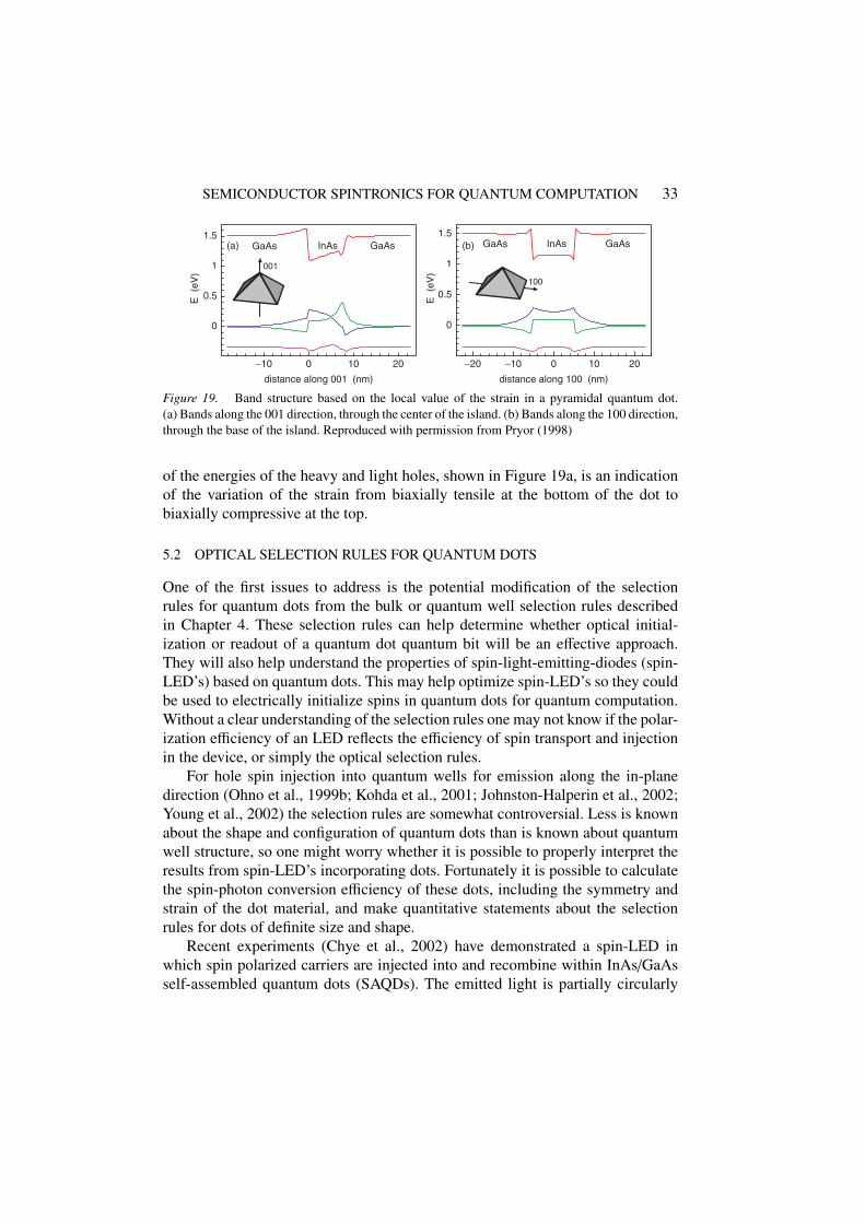
SEMICONDUCTOR SPINTRONICS FOR QUANTUM COMPUTATION 33
!10 0 10 20
distance along 001 (nm)
0
0.5
1
1.5
E (
eV)
GaAs GaAsInAs(a)
!20 !10 0 10 20
distance along 100 (nm)
0
0.5
1
1.5
E (
eV)
GaAs GaAsInAs(b)
001
100
Figure 19. Band structure based on the local value of the strain in a pyramidal quantum dot.(a) Bands along the 001 direction, through the center of the island. (b) Bands along the 100 direction,through the base of the island. Reproduced with permission from Pryor (1998)
of the energies of the heavy and light holes, shown in Figure 19a, is an indicationof the variation of the strain from biaxially tensile at the bottom of the dot tobiaxially compressive at the top.
5.2 OPTICAL SELECTION RULES FOR QUANTUM DOTS
One of the first issues to address is the potential modification of the selectionrules for quantum dots from the bulk or quantum well selection rules describedin Chapter 4. These selection rules can help determine whether optical initial-ization or readout of a quantum dot quantum bit will be an e!ective approach.They will also help understand the properties of spin-light-emitting-diodes (spin-LED’s) based on quantum dots. This may help optimize spin-LED’s so they couldbe used to electrically initialize spins in quantum dots for quantum computation.Without a clear understanding of the selection rules one may not know if the polar-ization e"ciency of an LED reflects the e"ciency of spin transport and injectionin the device, or simply the optical selection rules.
For hole spin injection into quantum wells for emission along the in-planedirection (Ohno et al., 1999b; Kohda et al., 2001; Johnston-Halperin et al., 2002;Young et al., 2002) the selection rules are somewhat controversial. Less is knownabout the shape and configuration of quantum dots than is known about quantumwell structure, so one might worry whether it is possible to properly interpret theresults from spin-LED’s incorporating dots. Fortunately it is possible to calculatethe spin-photon conversion e"ciency of these dots, including the symmetry andstrain of the dot material, and make quantitative statements about the selectionrules for dots of definite size and shape.
Recent experiments (Chye et al., 2002) have demonstrated a spin-LED inwhich spin polarized carriers are injected into and recombine within InAs/GaAsself-assembled quantum dots (SAQDs). The emitted light is partially circularly

34 SEMICONDUCTOR SPINTRONICS FOR QUANTUM COMPUTATION
polarized, with the degree of polarization providing a measure of the spin in theSAQDs. The conversion of electron spin to photon polarization is filtered throughthe selection rules associated with the quantum well or dot. In Chye et al. (2002),spin polarized electrons or holes were injected along the [001] growth directionfrom a (Ga,Mn)As layer that was spin polarized along [110]. The light emittedalong the [110] direction was found to be only /1% circularly polarized, suggest-ing a small spin polarization within the SAQD. However, due to the selection ruleuncertainty, a small photon polarization does not necessarily mean that the spinpolarization within the SAQD was small.
Pryor and Flatte (2003) calculated the circular polarization dependence ofdipole recombination from spin polarized states within a self-assembled InAs/GaAs quantum dot to provide a measure of the e"ciency with which spin po-larized SAQD states are converted into circularly polarized photons. Calculationswere done for a range of sizes and shapes. The polarization was independent ofwhether the injected spin polarized carriers are electrons or holes. The resultsshowed that the SAQD geometry and emission direction strongly influenced theobserved circular polarization, which varied from 0 to /20% (for 100% polarizedcarriers). For a lens-shaped SAQD there is a nonzero polarization for directionsperpendicular to the growth direction only if the SAQD is elongated so as to breakazimuthal symmetry. That elongation is indicated by e, which is the ratio of thesemi-major to semi-minor axes of the dot footprint. Measuring along the growthdirection, however, gives near unity conversion of spin to photon polarization, andis the least sensitive to uncertainties in SAQD geometry.
The situation considered by Pryor and Flatte (2003) had the electron spin po-larized along a direction d and the emitted light observed along the same direction.The emitted light was characterized by its degree of polarization defined by
Pd =(I+d " I"d )(I+d + I"d )
, (49)
where I±d is the intensity of light with ± helicity. The InAs SAQD was taken to bean ellipsoidal cap, ellongated along [110] and surrounded by GaAs.
Pryor and Flatte (2003) calculated ground state electron and hole wave func-tions using eight-band strain-dependent k·p theory in the envelope approximation,by a method that has been described above (Pryor et al., 1997; Pryor, 1998). Allwave functions were computed numerically on a real space grid with spacingset to the unstrained lattice constant of GaAs. Since strain and confinement splitthe HH/LH degeneracy, all levels are doubly degenerate, with states that may bedenoted |'- and T |'-, which are time-reverses of each other. Because the wavefunctions were computed with a spin-independent Hamiltonian, the state |'- has arandom spin orientation. Spin polarized states were constructed by taking a linearcombination of the states comprising the doublet, and adjusting the coe"cient so

SEMICONDUCTOR SPINTRONICS FOR QUANTUM COMPUTATION 35
as to maximize the expectation value of the pseudospin operator projected onto adirection d. That is, the complex number a that maximizes
10'| + a+0'|T 2 d · S 1|'- + aT |'-2
(1 + |a|2)(50)
was found, where the pseudospin operator in the eight-band model is given by
S =
)********+
!&6 0 00 J&8 00 0 !&7
,--------. (51)
and ! and J are the spin-1/2 and spin-3/2 angular momentum operators respec-tively. The spin-polarized states found this way are the eigenstates in a smallmagnetic field oriented parallel to d, i.e. for B < (mc/e!)#E, where #E is theenergy splitting of the top two orbital conduction states (for electrons) or va-lence states (for holes). For the systems considered the minimum #E is 20 meV(for holes), thus B < 100 T. Coulomb interaction between the electron and holedoes not appreciably change the results (Pryor and Flatte (2003) find a maximumchange in the polarization of 0.05 P).
For spin-polarized electrons and unpolarized holes, the intensity for emissionof circularly polarized light is given by
I±d = |0'v|"±d · p|'c-|2 + |0'v|T "±d · p|'c-|2, (52)
where |'v- and |'c- are the conduction and valence states with spin oriented alongd, p is the momentum operator, and "±d is the circular polarization vector for ±helicity with propagation along the direction d. The corresponding expression forspin polarized holes and unpolarized electrons is
I±d = |0'v|"±d · p|'c-|2 + |0'v|"±d · p T |'c-|2. (53)
However, since T and p anticommute, Eqs. (52) and (53) give identical results.For axially symmetric dots (e = 1) the polarization is zero, but increases as
the dots become more elongated. The polarization also increases with increasingEg with all other parameters held fixed. Finally, for a fixed elongation and fixedband gap, shorter dots have a larger polarization. Taken together, these indicate ageneral trend that the larger deviations from spherical symmetry result in largerpolarization, whether comparing dimensions in the [110] vs [110] or [001] vs[110].
The magnitude of the polarization is of great interest, since the experimentallyobserved polarizations were only on the order of 1%. For the geometries consid-ered, Pryor and Flatte (2003) found P[110] ! 23%. Assuming nominal valuese = 1.2, h = 2.3, and Eg = 1.25 eV Figure 20 shows that for 100% polarized

36 SEMICONDUCTOR SPINTRONICS FOR QUANTUM COMPUTATION
1.0 1.1 1.2 1.3 1.40.00
0.05
0.10
0.15
0.20
0.25
e
P[1
10]
Eg=1.25 eV
h=2.8 nmh=2.3 nmh=1.7 nm
(a)
1.20 1.25 1.300.00
0.05
0.10
0.15
0.20
0.25
Eg (eV)
P[1
10]
h=2.8 nmh=2.3 nmh=1.7 nm
e=1.2(b)
Figure 20. (a) Polarization along [110], as a function of elongation. (b) Polarization along [110],as a function of band gap. Reproduced with permission from Pryor and Flatte (2003)
carriers, the light should be 5% circular polarized. This value of 0.05 for theconversion e"ciency suggests the observed 1% circular polarization (Chye et al.,2002) was generated by carriers that were (1/0.05)% = 20% polarized. As the po-larization’s dependence on elongation is roughly linear, an average elongation fora dot ensemble would produce an average polarization roughly given by Figure 20as well.
5.3 THE RESPONSE OF QUANTUM DOT SPINS TO A MAGNETIC FIELD
The Lande g factor of electron and hole spins in quantum dots is also a topicof considerable interest. Confinement of the electrons and holes in the quantumdots modifies the g factors. As the confinement can be changed by an appliedelectric field the g factors can also be changed with a gate field. An experimentaldemonstration (Kato et al., 2003) of driving spin resonance with this e!ect inquantum wells suggests that single spins can also be manipulated in quantum dotsthis way. An elegant method of manipulating these spins utilizes the tensor natureof the g factor, and involves modifying the relative values of the tensor alongdi!erent directions. The Hamiltonian for such a spin would be
H = µB · g · S = !" · S, (54)
where " = B · g. Thus even for a static applied magnetic field, if the componentsof the g tensor change in relative magnitude the precession vector for the spin" could alter its direction. Representing this as a static component to " and atime-dependent transverse component produces the same phenomenon of spinresonance that can be achieved with a time-dependent magnetic field and a static g.
The electron g factor has been measured optically (Gupta et al., 1999; Bayeret al., 1999; Goni et al., 2000; Tischler et al., 2002) and electrically (Kouwenhovenet al., 2001; Medeiros-Ribeiro et al., 2002; Hanson et al., 2003; Medeiros-Ribeiro

SEMICONDUCTOR SPINTRONICS FOR QUANTUM COMPUTATION 37
et al., 2003). For large dots (Darnhofer et al., 1994; Kouwenhoven et al., 2001;Hanson et al., 2003; Valın-Rodrıguez et al., 2004), such as those defined litho-graphically (Kouwenhoven et al., 2001) or by electrical gates (Hanson et al.,2003), the magnetic fields of interest are usually large enough that the magneticlength is smaller than the dot diameter. In this limit the g factors are closely relatedto those of quantum wells, and theory (Valın-Rodrıguez et al., 2004) appears toagree with experiment (Hanson et al., 2003). The theoretical situation is muchless satisfactory for small dots—asymmetric structures grown by self assemblyin the molecular beam epitaxy (MBE) growth process or spherical nanocrystalsgrown by chemical synthesis. Although several phenomena known to a!ect g-factors in quantum wells (Ivchenko and Pikus, 1997; Winkler, 2003) have beenexplored in quantum dots (Kiselev et al., 1998; Krasny et al., 2001; Nenashevet al., 2003; Prado et al., 2003; Rodina et al., 2003; Prado et al., 2004; Schrierand Birgitta Whaley, 2003), the electronic states in dots are discrete, and thusdi!er qualitatively from semiconductors with unbounded motion in one or moredirections (Bimberg et al., 1998).
Semiconductor quantum dots also have fully coherent orbital electronic stateswith very long-lived spin coherence (Gupta et al., 1999), so the physics of theirg factors is very di!erent from that of metallic nanoparticles (Brouwer et al.,2000; Matveev et al., 2000; Petta and Ralph, 2002) (whose g factors are dominatedby e!ects from incoherent orbital scattering and spin scattering). The orbital co-herence of semiconductor quantum dot wavefunctions makes many dot properties,such as the sharply-peaked optical transitions, resemble those of atoms more thanbulk semiconductors. If quantum dots are considered as “artificial atoms” andapproached with techniques developed for magnetic atom dopants in solids (VanVleck, 1932), then the relevant quantity is the ratio of the energy splitting betweendi!erent angular momentum states to the spin–orbit interaction, and for a strongconfining potential the g factor of dots should approach 2.
Pryor and Flatte (2006a) showed that the g factor of a ground state electronor hole in a quantum dot depends significantly on an atom-like property: thequenching of orbital angular momentum through quantum confinement. In bulksemiconductors the conduction-band g factor is (Roth et al., 1959),
g = 2 " 2EP#
3Eg(Eg + #), (55)
where Eg is the band gap, # is the spin–orbit coupling, EP = 20S |P|X-2/m is theKane energy involving S-like and P-like Bloch functions 0S | and 0X| respectively(Ivchenko and Pikus, 1997), and m is the free electron mass. For unstrained spher-ical InAs nanocrystals with hard wall boundary conditions only Eg changes, yetEq. (55) is a very poor predictor of g factors in these dots (Figure 21). Similarconclusions can be obtained for InAs dots formed by self-assembly in MBE on

38 SEMICONDUCTOR SPINTRONICS FOR QUANTUM COMPUTATION
-16
-14
-12
-10
-8
-6
-4
-2
0
2
0.80.4 1.00.6 1.2
Eg (eV)
bulk InAs
nanocrystal
Figure 21. Electron g factor for a spherical unstrained InAs quantum dot embedded in vacuum.The dashed line indicates the result of Eq. (55) and the solid line the calculations in Pryor and Flatte(2006a). Reproduced with permission from Pryor and Flatte (2006a)
GaAs substrates (Pryor and Flatte, 2006a). Thus the bulk-like approach to g fac-tors in these quantum dots, averaging the g factors over the dot and barrier material(Kiselev et al., 1998; Rodina et al., 2003), also fails. The competing influence ofatom-like and bulk-like e!ects predict that the growth-direction electron g fac-tor increases with increasing dot size, whereas considering only bulk-like e!ectsleads to the opposite result. The results in Pryor and Flatte (2006a) agree withrecent experiments on electron g factors (Medeiros-Ribeiro et al., 2003).
Pryor and Flatte (2006a) presented calculations of quantum dot g factors atT = 0 K using eight-band strain dependent k · p theory in the envelope approx-imation with finite di!erences on a real space grid (Pryor, 1998). g came fromthe spin splitting in a magnetic field of |B| = 0.1 T and the sign of g from thespin direction of the lower energy state (parallel or anti-parallel to /B). Materialparameters were taken from Vurgaftman et al. (2001).
The magnetic field was included by coupling to both the envelope functionand the electron spin. The envelope was coupled to /B by making all di!erenceoperators covariant using the standard prescription for introducing gauge fieldson a lattice. For example,
'(/r + ! x) " '(/r " ! x)2!
1 '(/r + ! x)Ux(/r) " '(/r " ! x)U†x(/r " ! x)2!
, (56)
where ! is the grid spacing and Ux(/r) is the phase acquired by an electronhopping from the site at /r to the site at /r + ! x. The U’s were determined by

SEMICONDUCTOR SPINTRONICS FOR QUANTUM COMPUTATION 39
the requirement that transport around a plaquette produced the Aharonov–Bohmphase corresponding to the encircled flux, for example,
Ux(/r)Uy(/r + ! x)U†x(/r + !y)U†y (/r) = exp(i!2B2e/!), (57)
where B2 is the magnetic field component perpendicular to the plaquette. Theelectron spin was coupled to /B though a Pauli term for the Bloch functions,given by
Hs =µB
2/B ·
)********+
2/# 0 00 4
3/J 0
0 0 23 /#
,--------. , (58)
where µB is the Bohr magneton and /# and /J are the spin matrices for spin 1/2and 3/2 respectively. The g factors for the Bloch functions are 2, 4
3 , and 23 for
the conduction, valence, and spin–orbit bands respectively. The Bloch function gfactors are determined solely by the angular momentum of the Bloch states.
To see the origin of the discrepancy between the Roth expression of Eq. (55)and the results in Figure 21 consider the known origin of the e!ective g for con-duction electrons in a bulk semiconductor (Roth et al., 1959). When a magneticfield is applied, the orbital part of the wavefunction is modified into Landaulevels, corresponding to quantized orbital angular momentum along the axis ofthe magnetic field. In a single band model the Landau levels’ orbital angularmomentum comes from the envelope function alone. When the conduction andvalence bands are coupled, there is also a contribution from the valence Blochfunctions, which have a significant spin–orbit coupling. The Zeeman energy nowsplits the lowest Landau level into two spin-polarized Landau levels, one with spinparallel to the quantized orbital angular momentum and one antiparallel. Althoughthe bare g = 2 lowers the energy of the parallel spin state and raises that of theantiparallel state, the spin-orbit interaction preferentially aligns spin antiparallelto the orbital angular momentum. When that e!ect is absorbed into an e!ective g,it makes g < 2.
To isolate the e!ects of angular momentum quenching from those due to strainand spherical symmetry breaking Figure 21 shows results from unstrained spheri-cal InAs nanocrystals (Pryor and Flatte, 2006a). The calculations were done witha high barrier (10 eV) to avoid any leakage of the wavefunction outside the dot.For large dots (Eg ( 0.41 eV) the calculation agrees with the bulk-like formula(Roth et al., 1959), however it rapidly diverges from Roth et al. (1959) for smallerdots; when the confinement energy equals the bulk band gap of InAs the devi-ation from g " 2 predicted by Eq. (55) is six times larger than the actual value.Hole g factors for these nanocrystals show similar evidence of orbital angularmomentum quenching. Note that the quenching of orbital angular momentum forthe electron and hole states is compatible with the high fidelity selection rules for

40 SEMICONDUCTOR SPINTRONICS FOR QUANTUM COMPUTATION
generating spin-polarized carriers in dots with optical means (Pryor and Flatte,2003), because the optical transitions connect states with specific angular mo-mentum (valence and conduction) whereas the g factors probe how much angularmomentum admixture is possible for B ! 0.
5.4 SPIN-AC STARK EFFECTS IN QUANTUM DOTS
The spin-AC Stark e!ect permits the optically controlled spin manipulation ofindividual spin states. Although it has been seen in atoms (Rosatzin et al., 1990),the much larger oscillator strengths of quantum dots should permit much largere!ects. In a spin-selective AC Stark e!ect a quantum dot is illuminated with asingle intense pulse of circularly-polarized nonresonant light. Such a pulse shiftsthe energies of dot states, and due to di!ering transition matrix elements the twospin states are shifted di!erently. Hence this pulse produces a splitting of the twolowest energy conduction states, even when they are coherently occupied by oneelectron (Pryor and Flatte, 2006b). The splitting of these two states (spin-up andspin-down) can be viewed as an optically-induced pseudo-magnetic field (/Be f f )oriented along the propagation direction of the incident light. Direct applicationof this approach to quantum computing is clear, for one well-known physicalrealization of a single qubit operation is a magnetic field applied to a spin fora definite period of time. As this pseudo magnetic field can be applied in theabsence of a real magnetic field, resonant oscillation of this precessing field is notrequired.
Spin-splittings of states in undoped CdSe quantum dots (Gupta and Awschalom,2001; Gupta et al., 2002) and coherent manipulation of ensembles of spins inZnMnSe quantum wells (Gupta et al., 2001) have been demonstrated experimen-tally. Early theoretical considerations of the AC Stark e!ect (Cohen-Tannoudjiand Dupont-Roc, 1972; Combescot and Combescot, 1988; Cohen-Tannoudji et al.,1998), however, focused on non-spin-selective shifts of energy levels. RecentlyPryor and Flatte (2006b) showed that the spin-AC Stark e!ect (1) produces coherentrotations of electron spin in quantum dots with one electron, (2) the rotation anglecan exceed - for reasonable experimental parameters, and (3) the error rates aretolerable for quantum computation.
The AC Stark e!ect with unpolarized light is a nonlinear e!ect wherebylight with photon energy tuned near to the absorption transition between twostates induces a level repulsion between the two states (Cohen-Tannoudji andDupont-Roc, 1972; Cohen-Tannoudji et al., 1998). In perturbation theory(Combescot and Combescot, 1988) this level repulsion depends on I f /0, where Iis the light intensity, f is the oscillator strength of the transition, and 0 is the de-tuning of the photon energy from the transition energy. When circularly polarizedlight illuminates a transition from the first valence state pair to the first conduction

SEMICONDUCTOR SPINTRONICS FOR QUANTUM COMPUTATION 41
0.5 1.0 1.5 2.0
!0.015!0.014!0.013!0.012!0.011!0.010!0.009!0.008!0.007
Eg (eV)
InAs/GaAs
InAs/InPInAs
CdSe
1!s
tark
d!st
ark
dEg
(meV
!1 )
0.00.51.01.52.02.53.03.54.04.5
0.5 1.0 1.5 2.0 2.502468
1012
1614
Eg (eV)
InAs
InAs/InP
InAs/GaAs
CdSe
! s
(b)(a)
)E (
meV
)
Figure 22. (a) Stark splittings as a function of the bandgap for a detuning of 30 meV for InAs,InAs/InP, InAs/GaAs, and CdSe quantum dots. The angle (s = #E0t/! is for an incident 200 fspulse with 109 W/cm2. (b) Sensitivity of (s to variations in the bandgap as a function of bandgapfor detuning of 100 meV. Reproduced with permission from Pryor and Flatte (2006b)
state pair in a crystal with spin–orbit interaction the oscillator strengths of thetransitions di!er considerably; this is the source of the e!ective spin splitting ofthe conduction state pair.
Pryor and Flatte (2006b) calculated optical Stark shifts non-perturbativelyusing a restricted basis of quantum dot wave functions calculated with eight-band k · p theory in the envelope approximation. Because of the larger bandgapand lack of strain, CdSe calculations were performed with a single-band modelfor the conduction band, and a four-band model for the valence band. The CdSecalculations were done for the zincblende form, and all material parameters weretaken from Madelung et al. (1982).
Pryor and Flatte (2006b) examined the e!ect of dot size on the spin splitting.Shown in Figure 22a are the splittings for a detuning of 30 meV for four systems.For spin manipulation it is useful to consider the precession angle associated witha light pulse of duration 0t, given by (s = #E0t/! where #E is the Stark spinsplitting between up and down conduction states. In the results that follow, theStark splittings are given in meV along with the corresponding (s for a 200 fspulse with power density 109 W/cm2. The (2 meV spin splitting seen in CdSeCQD’s agrees with that measured experimentally in undoped dots (Gupta andAwschalom, 2001).
Bit errors may arise from a variety of sources, such as nonlinear e!ects andfree-carrier excitation (Gupta et al., 2001). Pryor and Flatte (2006b) focused on biterrors due to a persistent problem with quantum dot systems, nonzero linewidths.For measurements on an ensemble of dots, inhomogeneities in the dot size willyield a di!erent rotation angle for di!erent dots. For a quantum computer, inwhich individual dots will be selected, the finite line width of an individual statewill also cause some uncertainty in (s. To address this question, Pryor and Flatte(2006b) calculated numerical estimates of
1#E%#E(Eg, !.)%Eg
=1(s
%(s(Eg, !.)%Eg
, (59)

42 SEMICONDUCTOR SPINTRONICS FOR QUANTUM COMPUTATION
as shown in Figure 22b for a detuning of 100 meV. The results of Figure 22bmay be used to estimate the uncertainty in the rotation angle, #(s. For example,an ensemble measurement of InAs/InP dots with an inhomogeneous linewidthof 50 meV would give #(s / 0.5 for a --pulse, which should be su"cient topermit observation of a spin echo. For a single dot with a linewidth of 0.1 meV,#(s / 0.001, corresponding to a bit error rate of 10"6. This is su"ciently smallfor quantum error correction algorithms to apply (desirable error thresholds havebeen estimated (Preskill, 1998) at 10"5 " 10"6).
6 Spin-Selective Devices
One of the important quantum information capabilities proposed and developedis the capability of teleporting quantum information. Leuenberger et al. (2005)proposed a teleportation scheme for an arbitrary number of electronic qubits thatdoes not require an intermediate electronic qubit, or the use of external lasers toimplement a phase gate. Instead of generating and measuring Bell states betweenthe electronic qubits, this scheme relies on entangling both of the qubits with a sin-gle photon, yielding three-particle entanglement (a Greenberger–Horne–Zeilinger(GHZ) state (Greenberger et al., 1989)) of the qubit-photon-qubit Hilbert space.Any qubit that can be entangled with a photon can be used, but for specificityLeuenberger et al. (2005) considered qubits encoded in the electron spin of in-dividual quantum dots. The establishment of spin–photon entanglement can thenoccur naturally through conditional Faraday rotation in a microcavity. The en-tanglement of the destination qubit and the photon can be performed first, andthis photon can be retained at the origin before it is entangled with the originqubit, thus this procedure is teleportation, not quantum transmission. The sendingof the photon from the destination to the origin, after it is entangled with thedestination qubit, is the step corresponding to the distribution of EPR pairs inteleportation. The EPR pairs of Leuenberger et al. (2005), however, are a hybridconsisting of an entangled electronic spin and photon polarization. Teleportationcan then be implemented using only single-photon measurements: measurementof the polarization of the photon entangled with both qubits, and measurement ofthe spin orientation of the origin qubit via a single photon.
Described below in detail is the teleportation scheme of Leuenberger et al.(2005) for one qubit. Consider one excess electron in one quantum dot in a generalsingle-spin state
3333'(1)e4= ) |%- + * |&-, where the quantization axis is the z axis.
The photon propagating in the "z direction is initially linearly polarized in the xdirection, and interacts first with the destination spin, which is initialized parallelto x. Thus the destination spin–photon wavefunction initially is
3333'(1)pe)4= |3- |4)-.
The orientation of the spin a!ects the possible virtual processes excited by thephoton, two of which are shown in Figure 23. For spin-%, light of #+(z) polarization

SEMICONDUCTOR SPINTRONICS FOR QUANTUM COMPUTATION 43
3/2
Sz=1/2
(z)
Jz
HH
1/2 !1/2!3/2
HHLHLH
(z)
conduction
valence
HHHHLHLH
HHHHLHLH
absorb
abso
rb
HHHHLHLH
(z)
emit(z)
emit
h*d-
Figure 23. Selection rules for a photon propagating in the z direction and an excess spin-% electronin the dot. #+(z) can be virtually absorbed (upper right) by exciting an electron and a heavy hole, and#"(z) by exciting an electron and a light hole (lower left). !.d is the detuning of the nonresonantphoton from the transition energy. Reproduced with permission from Leuenberger et al. (2005)
excites an electron and heavy hole (upper right, Figure 23), and light of #"(z)polarization excites an electron and a light hole (lower left, Figure 23). In bothcases the selection rules and Pauli blocking force the light subsequently emittedfrom electron–hole recombination to have the same polarization as was absorbed,and the final occupations of electron states in the dot (lower right, Figure 23)are the same as the initial occupations. These virtual processes have di!erentprobabilities, however, and this leads to Faraday rotation: a phase shift eiS hh
0 of#+(z) and eiS lh
0 of #"(z). If, however, the spin were & instead the phase shift of #+(z)
light would be eiS lh0 and of #"(z) would be eiS hh
0 . Thus there is a conditional Faradayrotation of the components of the electron–photon state depending on the photonpolarization and spin orientation.
After the interaction of the initially unentangled photon with the spin in thequantum dot, the resulting electron–photon state is
3333'(1)pe)4= eiS hh
0
3333'(1)hh
4+ eiS lh
0
3333'(1)lh
4, (60)
where3333'(1)
hh
4=
53333#+(z)
4|%)- +
3333#"(z)
4|&)-
6/2 originates from the virtual process
where a photon creates an electron and a heavy hole, and3333'(1)
lh
4=53333#"(z)
4|%)-+
3333#+(z)
4|&)-
6/2 originates from the virtual process where the photon creates an

44 SEMICONDUCTOR SPINTRONICS FOR QUANTUM COMPUTATION
electron and a light hole. Both3333'(1)
hh
4and
3333'(1)lh
4are EPR states. The photon state
|1- = cos1 |3- + sin1 |5- has a linear polarization rotated by 1 around the z axiswith respect to the state |3- of linear polarization in the x direction, and can bewritten |1- =
5e"i1
3333#+(z)
4+ ei1
3333#"(z)
46/.
2. Consequently,
3333'(1)pe)4=
ei(S hh0 +S lh
0 )/2.
2
7|"S 0/2-
333%)8 + |+S 0/2-333&)8
9, (61)
where S 0 = S hh0 " S lh
0 . Thus the spin–photon interaction produces a conditionalsingle-photon Faraday rotation around the z axis by the angle ±S 0/2. If S 0 = -/2,the linear polarization of the incoming photon is rotated "-/4 by the spin up com-ponent, and at the same time is rotated +-/4 by the spin down component, yieldingtwo orthogonal photon polarizations. Thus
3333'(1)pe)4= (|67- |%)- + |89- |&)-) /
.2,
which is maximally entangled. In order to enhance the spin–photon interactionsu"ciently to achieve S 0 = -/2, each quantum dot should be placed in its ownmicrocavity. Using a switchable cavity permits the precise control of the Faradayrotation angle S 0/2 necessary for high fidelity teleportation. After interacting witha spin at a destination (D)) the photon is sent to an origin (D), and can be retainedas a resource for teleportation from D to D) until the spin at D) decoheres. Forcoherence times of 100 ns (Kikkawa and Awschalom, 1998) the maximum tele-portation distance (determined by the speed of light) would be (15 m and for10 ms (Kroutvar et al., 2004) it is 1.5 , 106 m.
When it is time to teleport the spin at D to D) the photon is permitted to interactwith the quantum dot at D, giving rise to a GHZ state in the hybrid spin–photon-spin system. After this interaction
3333'(1)epe)
4= ei(S hh
0 +S lh0 )/2 7) |%- |"S 0/2 " -/4-
333%)8 + ) |%- |"S 0/2 + -/4-333&)8
+* |&- |+S 0/2 " -/4-333%)8 + * |&- |+S 0/2 + -/4-
333&)89/.
2. (62)
Choosing S 0 = -/2,3333'(1)
epe)4='|5-
7") |%-
333%)8 + * |&-333&)8
9+ |3-
7) |%-
333&)8 + * |&-333%)8
9(/.
2. (63)
Changing to the S x representation for the spin at D yields3333'(1)
epe)4=
:|5-
'|4-
7")
333%)8 + *333&)8
9+ |1-
7")
333%)8 " *333&)8
9(
+ |3-'|4-
7*333%)8 + )
333&)89+ |1-
7*333%)8 " )
333&)89(;/.
2. (64)
Performing the correct measurements completes the teleportation. If the linearpolarization of the photon is measured first, then depending on the two initialspin orientations [see Eq. (63)], collapse of the wavefunction leaves the qubits

SEMICONDUCTOR SPINTRONICS FOR QUANTUM COMPUTATION 45
at D and at D) in one of the four Bell states. After performing a single-spinmeasurement in the x direction of the spin at D (which, as described below,can be done with a single photon), the spin state at D) is projected onto [seeEq. (64)]
3333'(1)e1
4= ") |%)-+* |&)-,
3333'(1)e2
4= ") |%)-"* |&)-,
3333'(1)e3
4= * |%)-+) |&)-, or3333'(1)
e4
4= * |%)-") |&)-with equal probability. These projections correspond exactly
to the states obtained in Bennett et al. (1993). After communicating classically theoutcome of the measurement of the linear polarization of the photon and D’s spinorientation along Sx to D), the original spin state of D can be reconstructed atD) and teleportation is complete. The same amount of classical communication(two bits) is required for this approach as was required in Bennett et al. (1993).However, no intermediate electronic qubit was required, and the measurementsare simply performed with single photons.
Faraday rotation to entangle the photon and electron spin [Eq. (60)] also pro-vides the way to measure the spin with a single photon. Leuenberger et al. (2005)assumes that the microcavities have an additional resonant mode at a di!erentfrequency for photons propagating in the x direction. Equation (60) shows thatif the spin on the quantum dot points in the +x ("x) direction, this incominglinearly polarized photon is converted into an outgoing circularly polarized pho-ton #+(x) (#"(x)). Measuring the circular polarization of the photon after it escapesyields the spin orientation along x. Electrical single-spin measurements at D coulduse instead a single electron transistor (SET), converting the spin information tocharge information (Loss and DiVincenzo, 1998; Friesen et al., 2004). Each of thesteps along the way could be performed with high fidelity (time-correlated singlephoton counting permits a counting e"ciency close to one (Becker et al., 2001)).
7 Conclusion
This chapter has described several properties of spin that may be relevant tothe successful achievement of high-fidelity quantum operations within a quan-tum computer. The transport and persistence of spin orientation in an ensemblehas been described, which may assist in the preparation of highly oriented spinsto initialize a quantum computer. Approaches to accurately calculate the spin-dependent electronic structure of bulk, quantum well, and quantum dot nanostruc-tures have been described. Methods of initialization, manipulation, and detectionof coherence in ionic degrees of freedom have been identified. The use of ionicspins may permit highly uniform systems of physical qubits to be generated.Techniques for initializing and optically manipulating spins in quantum dots havebeen presented, along with the physical origin of the Lande g factor in quantumdots.
At this point it appears too early to know what approach will most rapidlyapproach a scalable quantum computer in the solid state. Some approaches started

46 SEMICONDUCTOR SPINTRONICS FOR QUANTUM COMPUTATION
earlier, such as manipulation via the exchange interaction in lithographic quantumdots, are now making rapid progress (Petta et al., 2005). The seven years betweenthe proposal of a quantum dot architecture for a quantum computer (Loss andDiVincenzo, 1998) and the successful observation of single-spin decoherencetimes in a quantum dot (T +2 , as they were in a nuclear spin ensemble) (Pettaet al., 2005) provides some indication of the potential time between proposal andsuccessful demonstration in the field of solid-state quantum computation.
Acknowledgments
I would like to acknowledge D. D. Awschalom, T. F. Boggess, K. C. Hall,W. H. Lau, J. Levy, M. Leuenberger, J. T. Olesberg, C. E. Pryor, J.-M. Tang, andZ. G. Yu. This work was supported in part by DARPA, ARO, and ONR.
References
Aronov, A. G. and Pikus, G. E. (1976) Spin injection into semiconductors, Fiz. Tekh. Poluprovodn.10, 1177–1179, [Sov. Phys. Semicond. 10, 698–700 (1976)].
Arseev, P. I., Maslova, N. S., Panov, V. I., Savinov, S. V., and van Haesendock, C. (2003) Many-Particle Interaction in Tunneling Spectroscopy of Impurity States on the InAs(110) Surface,Pis’ma Zh. Eksp. Teor. Fiz. 77, 202–207, [JETP Lett. 77, 172 (2003)].
Awschalom, D. D., Samarth, N., and Loss, D. (eds.) (2002) Semiconductor Spintronics andQuantum Computation, Heidelberg, Springer Verlag.
Barenco, A., Bennett, C. H., Cleve, R., DiVincenzo, D. P., Margolus, N., Shor, P., Sleator, T.,Smolin, J. A., and Weinfurter, H. (1995) Elementary gates for quantum computation, Phys.Rev. A 52, 3457–3467.
Bayer, M., Kuther, A., Forchel, A., Gorbunov, A., Timofeev, V. B., Schafer, F., Reithmaier, J. P.,Reinecke, T. L., and Walck, S. N. (1999) Electron and Hole g Factors and Exchange Interactionfrom Studies of the Exciton Fine Structure in In0.60Ga0.40As Quantum Dots, Phys. Rev. Lett. 82,1748–1751.
Becker, W., Bergmann, A., Koenig, K., and Tirlapur, U. (2001) Picosecond fluorescence lifetimemicroscopy by TCSPC imaging, Proc. SPIE 4262, 414–419.
Bennett, C. H. and DiVincenzo, D. P. (2000) Quantum information and computation, Nature 404,247–255.
Bennett, C. H., Brassard, G., Crepeau, C., Jozsa, R., Peres, A., and Wootters, W. K. (1993) Teleport-ing an unknown quantum state via dual classical and Einstein-Podolsky-Rosen channels, Phys.Rev. Lett. 70, 1895–1899.
Bhat, R. D. R. and Sipe, J. E. (2000) Optically Injected Spin Currents in Semiconductors, Phys.Rev. Lett. 85, 5432–5435.
Bimberg, D., Grundmann, M., and Ledentsov, N. N. (1998) Quantum Dot Heterostructures, NewYork, Wiley.
Boggess, T. F., Olesberg, J. T., Yu, C., Flatte, M. E., and Lau, W. H. (2000) Room-temperatureelectron spin relaxation in bulk InAs, Appl. Phys. Lett. 77, 1333–1335.
Brouwer, P. W., Waintal, X., and Halperin, B. I. (2000) Fluctuating Spin g-Tensor in Small MetalGrains, Phys. Rev. Lett. 85, 369–372.

SEMICONDUCTOR SPINTRONICS FOR QUANTUM COMPUTATION 47
Bychkov, Y. A. and Rashba, E. I. (1984) Oscillatory e!ects and the magnetic susceptibility ofcarriers in inversion layers, J. Phys. C 17, 6039–6045.
Cardona, M., Christensen, N. E., and Fasol, G. (1988) Relativistic band structure and spin-orbitsplitting of zinc-blende-type semiconductors, Phys. Rev. B 38, 1806–1827.
Chye, Y., White, M. E., Johnston-Halperin, E., Gerardot, B. D., Awschalom, D. D., and Petro!,P. M. (2002) Spin injection from (Ga,Mn)As into InAs quantum dots, Phys. Rev. B 66, 201301.
Cohen-Tannoudji, C. and Dupont-Roc, J. (1972) Experimental Study of Zeeman Light Shifts inWeak Magnetic Fields, Phys. Rev. A 5, 968–984.
Cohen-Tannoudji, C., Dupont-Roc, J., and Grynberg, G. (1998) Atom-Photon Interactions, NewYork, Wiley.
Combescot, M. and Combescot, R. (1988) Excitonic Stark Shift: A Coupling to ”Semivirtual”Biexcitons, Phys. Rev. Lett. 61, 117–120.
Darnhofer, T., Broido, D. A., and Rossler, U. (1994) Dipole spectra of holes in quantum dots, Phys.Rev. B 50, 15412–15415.
Datta, S. and Das, B. (1990) Electronic analog of the electro-optic modulator, Appl. Phys. Lett. 56,665–667.
DiVincenzo, D. P., Bacon, D., Kempe, J., Burkard, G., and Whaley, K. B. (2000) Universal quantumcomputation with the exchange interaction, Nature 408, 339–342.
Durkan, C. and Welland, M. E. (2002) Electronic spin detection in molecules using scanning-tunneling-microscopy-assisted electron-spin resonance, Appl. Phys. Lett. 80, 458–460.
D’yakonov, M. I. and Kachorovskii, V. Y. (1986) Spin relaxation of two-dimensional electrons innoncentrosymmetric semiconductors, Soviet Phys. Semiconductors 20, 110–112.
D’yakonov, M. I. and Perel’, V. I. (1972) Spin relaxation of conduction electrons in noncentrosym-metric semiconductors, Soviet Phys. Solid State 13, 3023–3026.
Edelstein, V. M. (1990) Spin polarization of conduction electrons induced by electric current intwo-dimensional asymmetric electron systems, Solid State Commun. 73, 233–235.
Elzerman, J. M., Hanson, R., van Beveren, L. H. W., Witkamp, B., Vandersypen, L. M. K., andKouwenhoven, L. P. (2004) Single-shot read-out of an individual electron spin in a quantumdot, Nature 430, 431–435.
Fert, A. and Campbell, I. A. (1968) Two-Current Conduction in Nickel, Phys. Rev. Lett. 21, 1190–1192.
Fert, A. and Ja!res, H. (2001) Conditions for e"cient spin injection from a ferromagnetic metalinto a semiconductor, Phys. Rev. B 64, 184420.
Flatte, M. E. and Byers, J. M. (2000) Spin Di!usion in Semiconductors, Phys. Rev. Lett. 84, 4220–4223.
Friesen, M., Tahan, C., Joynt, R., and Eriksson, M. A. (2004) Spin Readout and Initialization in aSemiconductor Quantum Dot, Phys. Rev. Lett. 92, 037901.
Goni, A. R., Born, H., Heitz, R., Ho!mann, A., Thomsen, C., Heinrichsdor!, F., and Bimberg,D. (2000) Magnetoluminescence Study of Annealing E!ects on the Electronic Structure ofSelf-organized InGaAs/GaAs Quantum Dots, Jpn J. Appl. Phys. 39, 3907–3914.
Greenberger, D. M., Horna, M. A., and Zeilinger, A. (1989) Going Beyond Bell’s Theorem, In Bell’sTheorem, Quantum Theory, and Conceptions of the Universe, Dordrecht, Kluwer Academic,pp. 73–76.
Gruber, A., Drabenstedt, A., Tietz, C., Fleury, L., Wrachtrup, J., and von Borczyskowski, C. (1997)Scanning Confocal Optical Microscopy and Magnetic Resonance on Single Defect Centers,Science 276, 2012–2014.
Gupta, J. A. and Awschalom, D. D. (2001) Spin precession and the optical Stark e!ect in asemiconductor-doped glass, Phys. Rev. B 63, 085303.

48 SEMICONDUCTOR SPINTRONICS FOR QUANTUM COMPUTATION
Gupta, J. A., Awschalom, D. D., Peng, X., and Alivisatos, A. P. (1999) Spin coherence insemiconductor quantum dots, Phys. Rev. B 59, R10421–R10424.
Gupta, J. A., Knobel, R., Samarth, N., and Awschalom, D. D. (2001) Ultrafast manipulation ofelectron spin coherence, Science 292, 2458–2561.
Gupta, J. A., Awschalom, D. D., Efros, A. L., and Rodina, A. V. (2002) Spin dynamics insemiconductor nanocrystals, Phys. Rev. B 66, 125307.
Hall, K. and Flatte, M. E. (2006) Performance of a spin-based insulated gate field e!ect transistor,Appl. Phys. Lett. 88, 162503.
Hall, K., Gundogdu, K., Altunkaya, E., Lau, W. H., Flatte, M. E., Boggess, T. F., Zinck, J. J.,Barvosa-Carter, W. B., and Skeith, S. L. (2003a) Spin relaxation in (110) and (001) InAs/GaSbsuperlattices, Phys. Rev. B 68, 115311.
Hall, K., Lau, W. H., Gundogdu, K., Flatte, M. E., and Boggess, T. F. (2003b) Nonmagneticsemiconductor spin transistor, Appl. Phys. Lett. 83, 2937–2939.
Hall, K., Gundogdu, K., Hicks, J. L., Kocbay, A. N., Flatte, M. E., Boggess, T. F., Holabird, K.,Hunter, A., Chow, D. H., and Zinck, J. J. (2005) Room-temperature electric-field controlledspin dynamics in (110) InAs quantum wells, Appl. Phys. Lett. 86, 202114.
Hanson, R., Witkamp, B., Vandersypen, L. M. K., van Beveren, L. H. W., Elzerman, J. M., andKouwenhoven, L. P. (2003) Zeeman Energy and Spin Relaxation in a One-Electron QuantumDot, Phys. Rev. Lett. 91, 196802.
Hanson, R., Kouwenhoven, L. P., Petta, J. R., Tarucha, S., and Vandersypen, L. M. K. (2006) Spinsin few-electron quantum dots, cond-mat/0610433.
Haynes, J. R. and Shockley, W. (1951) The Mobility and Life of Injected Holes and Electrons inGermanium, Phys. Rev. 81, 835–843.
Heinrich, A. J., Gupta, J. A., Lutz, C. P., and Eigler, D. M. (2004) Single-atom spin–flipspectroscopy, Science 306, 466–469.
Hubner, J., Ruhle, W. W., Klude, M., Hommel, D., Bhat, R. D. R., Sipe, J. E., and van Driel, H. M.(2003) Direct Observation of Optically Injected Spin-Polarized Currents in Semiconductors,Phys. Rev. Lett. 90, 216601.
Imamoglu, A., Awschalom, D. D., Burkard, G., DiVincenzo, D. P., Loss, D., Sherwin, M., andSmall, A. (1999) Quantum Information Processing Using Quantum Dot Spins and Cavity QED,Phys. Rev. Lett. 83, 4204–4207.
Ivchenko, E. L. and Pikus, G. E. (1997) Superlattices and Other Heterostructures, New York,Springer.
Jelezko, F., Popa, I., Gruber, A., Tietz, C., Wrachtrup, J., Nizovtsev, A., and Kilin, S. (2002) Singlespin states in a defect center resolved by optical spectroscopy, Appl. Phys. Lett. 81, 2160–2162.
Johnson, M. and Silsbee, R. H. (1988) Spin-injection experiment, Phys. Rev. B 37, 5326–5335.Johnston-Halperin, E., Lofgreen, D., Kawakami, R. K., Young, D. K., Coldren, L., Gossard, A. C.,
and Awschalom, D. D. (2002) Spin-polarized Zener tunneling in (Ga,Mn)As, Phys. Rev. B 65,041306.
Kane, B. E. (1998) A silicon-based nuclear spin quantum computer, Nature 393, 133–137.Karimov, O. Z., John, G. H., Harley, R. T., Lau, W. H., Flatte, M. E., Henini, M., and Airey, R.
(2003) High temperature gate control of quantum well spin memory, Phys. Rev. Lett. 91,246601.
Kato, Y., Myers, R. C., Gossard, A. C., Levy, J., and Awschalom, D. D. (2003) Gigahertz ElectronSpin Manipulation Using Voltage-Controlled g-Tensor Modulation, Science 299, 1201–1204.
Kikkawa, J. M. and Awschalom, D. D. (1998) Resonant Spin Amplification in n-Type GaAs, Phys.Rev. Lett. 80, 4313–4316.
Kikkawa, J. M. and Awschalom, D. D. (1999) Lateral drag of spin coherence in gallium arsenide,Nature 397, 139–141.

SEMICONDUCTOR SPINTRONICS FOR QUANTUM COMPUTATION 49
Kikkawa, J. M., Smorchkova, I. P., Samarth, N., and Awschalom, D. D. (1997) Room-TemperatureSpin Memory in Two-Dimensional Electron Gases, Science 277, 1284–1287.
Kiselev, A. A., Ivchenko, E. L., and Rossler, U. (1998) Electron g factor in one- and zero-dimensional semiconductor nanostructures, Phys. Rev. B 58, 16353–16359.
Kitchen, D. and Yazdani, A. (2005) Spatial Structure of a Single Mn Impurity State on GaAs (110)Surface, J. of Supercond. and Nov. Mag. 18, 23–28.
Kitchen, D., Richardella, A., Tang, J.-M., Flatte, M. E., and Yazdani, A. (2006) Atom-by-atomsubstitution of Mn in GaAs and Visualization of their hole-mediated interactions, Nature 442,436–439.
Kittel, C. and Kroemer, H. (1980) Thermal Physics, New York, W. H. Freeman and Company.Kohda, M., Ohno, Y., Takamura, K., Matsukura, F., and Ohno, H. (2001) A Spin Esaki Diode, Jpn
J. Appl. Phys. Part 2 40, L1274–L1276.Kouwenhoven, L. P., Austing, D. G., and Tarucha, S. (2001) Few-electron quantum dots, Rep. Prog.
Phys. 64, 701–736.Krasny, Y. P., Kovalenko, N. P., Krey, U., and Jacak, L. (2001) Paramagnetic-diamagnetic interplay
in quantum dots for nonzero temperatures, J. Phys. Cond. Mat. 13, 4341–4358.Kroutvar, M., Ducommun, Y., Heiss, D., Bichler, M., Schuh, D., Abstreiter, G., and Finley, J. J.
(2004) Optically programmable electron spin memory using semiconductor quantum dots,Nature 432, 81–84.
Lau, W. H. and Flatte, M. E. (2002) Tunability of electron spin coherence in III-V quantum wells,J. Appl. Phys. 91, 8682–8684.
Lau, W. H., Olesberg, J. T., and Flatte, M. E. (2001) Electron-spin decoherence times in bulk andquantum well zinc-blende semiconductors, Phys. Rev. B 64, 161301(R).
Lau, W. H., Olesberg, J. T., and Flatte, M. E. (2004) Electronic structures and electron spindecoherence in (001)-grown layered zincblende semiconductors, cond-mat/0406201.
Lee, T. C. and Anderson, W. W. (1964) Edge emission involving manganese impurities in GaAs at4.2: K, Solid State Commun. 2, 265–8.
Leuenberger, M. N., Flatte, M. E., and Awschalom, D. D. (2005) Teleportation of electronic many-qubit states via single photons, Phys. Rev. Lett. 94, 107401.
Levy, J. (2002) Universal quantum computation with spin-1/2 pairs and Heisenberg exchange, Phys.Rev. Lett. 92, 147902.
Loss, D. and DiVincenzo, D. P. (1998) Quantum computation with quantum dots, Phys. Rev. A 57,120–126.
Madelung, O., Schilz, M., and Weiss, H. (eds.) (1982) Landolt-Bornstein, Numerical Data andFunctional Relations in Science and Technology, New York, Springer.
Manassen, Y., Hamers, R. J., Demuth, J. E., and Castellano, Jr., A. J. (1989) Direct observation ofthe precession of individual paramagnetic spins on oxidized silicon surfaces, Phys. Rev. Lett.62, 2531–2534.
Matveev, K. A., Glazman, L. I., and Larkin, A. I. (2000) g-Factors of Discrete Levels inNanoparticles, Phys. Rev. Lett. 85, 2789–2792.
Medeiros-Ribeiro, G., Pinheiro, M. V. B., Pimentel, V. L., and Marega, E. (2002) Spin splitting ofthe electron ground states of InAs quantum dots, Appl. Phys. Lett. 80, 4229–4231.
Medeiros-Ribeiro, G., Ribeiro, E., and Westfahl, Jr., H. (2003) g-factor engineering and control inself-assembled quantum dots, Appl. Phys. A 77, 725–729.
Meier, F. and Zachachrenya, B. P. (1984) Optical Orientation: Modern Problems in CondensedMatter Science, Vol. 8, Amsterdam, North-Holland.
Mott, N. F. (1936) The Electrical Conductivity of Transition Metals, Proc. Royal Soc. of London A153, 699–717.

50 SEMICONDUCTOR SPINTRONICS FOR QUANTUM COMPUTATION
Nenashev, A. V., Dvurechenskii, A. V., and Zinovieva, A. F. (2003) Wave functions and g factor ofholes in Ge/Si quantum dots, Phys. Rev. B 67, 205301.
Ohno, Y., Terauchi, R., Adachi, T., Matsukura, F., and Ohno, H. (1999a) Spin relaxation inGaAs(110) quantum wells, Phys. Rev. Lett. 83, 4196–4199.
Ohno, Y., Young, D. K., Beschoten, B., Matsukura, F., Ohno, H., and Awschalom, D. D. (1999b)Electrical spin injection in a ferromagnetic semiconductor heterostructure, Nature (London)402, 790–792.
Olesberg, J. T., Lau, W. H., Flatte, M. E., Yu, C., Altunkaya, E., Shaw, E. M., Hasenberg, T. C.,and Boggess, T. F. (2001) Interface contributions to spin relaxation in a short-period InAs/GaSbsuperlattice, Phys. Rev. B 64, 201301(R).
Petta, J. R. and Ralph, D. C. (2002) Measurements of Strongly Anisotropic g Factors for Spins inSingle Quantum States, Phys. Rev. Lett. 89, 156802.
Petta, J. R., Johnson, A. C., Taylor, J. M., Laird, E. A., Yacoby, A., Lukin, M. D., Marcus, C. M.,Hanson, M. P., and Gossard, A. C. (2005) Coherent Manipulation of Coupled Electron Spins inSemiconductor Quantum Dots, Science 309, 2180–2184.
Prado, S. J., Trallero-Giner, C., Alcalde, A. M., Lopez-Richard, V., and Marques, G. E. (2003)Magneto-optical properties of nanocrystals: Zeeman splitting, Phys. Rev. B 67, 165306.
Prado, S. J., Trallero-Giner, C., Lopez-Richard, V., Alcalde, A. M., and Marques, G. E. (2004)Zeeman e!ect and magnetic anomalies in narrow-gap semiconductor quantum dots, Physica E20, 286–289.
Preskill, J. (1998) Fault Tolerant Quantum Computation, In H.-K. Lo, S. Popescu, and T. Spiller(eds.), Introduction to quantum computation and information, Singapore, World Scientific, pp.213–269.
Pryor, C. (1998) Eight-band calculations of strained InAs/GaAs quantum dots compared with one-,four-, and six-band approximations, Phys. Rev. B 57, 7190–7195.
Pryor, C., Pistol, M.-E., and Samuelson, L. (1997) Electronic structure of strained InP/Ga0.51In0.49Pquantum dots, Phys. Rev. B 56, 10404–10411.
Pryor, C. E. and Flatte, M. E. (2003) Accuracy of Circular Polarization as a Measure of SpinPolarization in Quantum Dot Qubits, Phys. Rev. Lett. 91, 257901.
Pryor, C. E. and Flatte, M. E. (2006a) Lande g Factors and Orbital Momentum Quenching inSemiconductor Quantum Dots, Phys. Rev. Lett. 96, 026804.
Pryor, C. E. and Flatte, M. E. (2006b) Predicted ultrafast single qubit operations in semiconductorquantum dots, Appl. Phys. Lett. 88, 233108.
Qi, Y., Yu, Z.-G., and Flatte, M. E. (2006) Spin Gunn E!ect, Phys. Rev. Lett. 96, 026602.Quintero, G. F. and Piermarocchi, C. (2005) Entanglement and errors in the control of spins by
optical coupling, Phys. Rev. B 72, 045334.Rashba, E. I. (1960) Properties of semiconductors with an extremum loop I. Cyclotron and combi-
national resonance in a magnetic field perpendicular to the plane of the loop, Soviet Phys. SolidState 2, 1109–1122.
Rashba, E. I. (2000) Theory of electrical spin injection: Tunnel contacts as a solution of theconductivity mismatch problem, Phys. Rev. B 62, R16267–R16270.
Rodina, A. V., Efros, A. L., and Alekseev, A. Y. (2003) E!ect of the surface on the electron quantumsize levels and electron g factor in spherical semiconductor nanocrystals, Phys. Rev. B 67,155312.
Rosatzin, M., Suter, D., and Mlynek, J. (1990) Light-shift-induced spin echoes in a J=1/2 atomicground state, Phys. Rev. A 42, 1839–1841.
Roth, L. M., Lax, B., and Zwerdling, S. (1959) Theory of Optical Magneto-Absorption E!ects inSemiconductors, Phys. Rev. 114, 90–104.

SEMICONDUCTOR SPINTRONICS FOR QUANTUM COMPUTATION 51
Rugar, D., Budakian, R., Mamin, H. J., and Chui, B. W. (2004) Single spin detection by magneticresonance force microscopy, Nature 430, 329–332.
Schmidt, G., Ferrand, D., Molenkamp, L. W., Filip, A. T., and van Wees, B. J. (2000) Fundamentalobstacle for electrical spin injection from a ferromagnetic metal into a di!usive semiconductor,Phys. Rev. B 62, R4790–R4793.
Schneider, J., Kaufmann, U., Wilkening, W., and Baeumler, M. (1987) Electronic structure of theneutral manganese acceptor in gallium arsenide, Phys. Rev. Lett. 59, 240–243.
Schrier, J. and Birgitta Whaley, K. (2003) Tight-binding g-factor calculations of CdSe nanostruc-tures, Phys. Rev. B 67, 235301.
Slichter, C. P. (1963) Principles of Magnetic Resonance, New York, Harper and Row.Smith, D. L. and Silver, R. N. (2001) Electrical spin injection into semiconductors, Phys. Rev. B
64, 045323.Steeves, G. M., Elezzabi, A. Y., and Freeman, M. R. (1998) Nanometer-scale imaging with an
ultrafast scanning tunneling microscope, Appl. Phys. Lett. 72, 504–506.Stevens, M. J., Smirl, A. L., Bhat, R. D. R., Najmaie, A., Sipe, J. E., and van Driel, H. M. (2003)
Quantum Interference Control of Ballistic Pure Spin Currents in Semiconductors, Phys. Rev.Lett. 90, 136603.
Tang, J.-M. and Flatte, M. E. (2004) Multiband tight-binding model of local magnetism inGa1"xMnxAs, Phys. Rev. Lett. 92, 047201.
Tang, J.-M. and Flatte, M. E. (2005) Spin-orientation-dependent spatial structure of a magneticacceptor state in a zincblende semiconductor, Phys. Rev. B 72, 161315(R).
Tang, J.-M., Levy, J., and Flatte, M. E. (2006) All-electrical control of single ion spins in asemiconductor, Phys. Rev. Lett. 97, 106803.
Terauchi, R., Ohno, Y., Adachi, T., Sato, A., Matsukura, F., Tackeuchi, A., and Ohno, H. (1999)Carrier Mobility Dependence of Electron Spin Relaxation in GaAs Quantum Wells, Jpn. J.Appl. Phys. Pt. 1 38, 2549–2551.
Tischler, J. G., Bracker, A. S., Gammon, D., and Park, D. (2002) Fine structure of trions and excitonsin single GaAs quantum dots, Phys. Rev. B 66, 081310.
Uenoyama, T. and Sham, L. J. (1990) Hole relaxation and luminescence polarization in doped andundoped quantum wells, Phys. Rev. Lett. 64, 3070–3073.
Valın-Rodrıguez, M., Puente, A., and Serra, L. (2004) Spin splitting and precession in quantum dotswith spin–orbit coupling: The role of spatial deformation, Phys. Rev. B 69, 085306.
Van Vleck, J. H. (1932) The Theory of Electric and Magnetic Susceptibilities, New York, Oxford.Vurgaftman, I., Meyer, J. R., and Ram-Mohan, L. R. (2001) Band parameters for III–V compound
semiconductors and their alloys, J. Appl. Phys. 89, 5815–5875.Winkler, R. (2003) Spin–orbit Coupling E!ects in Two-Dimensional Electron and Hole Systems,
Berlin, Springer.Winkler, R. and Rossler, U. (1993) General approach to the envelope-function approximation based
on a quadrature method, Phys. Rev. B 48, 8918–8927.Xiao, M., Martin, I., Yablonovitch, E., and Jiang, H. W. (2004) Electrical detection of the spin
resonance of a single electron in a silicon field-e!ect transistor, Nature 430, 435–439.Yafet, Y. (1963) g Factors and Spin-Lattice Relaxation of Conduction Electrons, Solid State Phys.
14, 2–98.Yakunin, A. M., Silov, A. Y., Koenraad, P. M., Roy, W. V., Boeck, J. D., and Wolter, J. H. (2004a)
Imaging of the (Mn2+3d5 + hole) complex in GaAs by cross-sectional scanning tunnelingmicroscopy, Physica E 21, 947–950.
Yakunin, A. M., Silov, A. Y., Koenraad, P. M., Roy, W. V., Boeck, J. D., Wolter, J. H., Tang, J.-M.,and Flatte, M. E. (2004b) Spatial structure of an individual Mn acceptor in GaAs, Phys. Rev.Lett. 92, 216806.

52 SEMICONDUCTOR SPINTRONICS FOR QUANTUM COMPUTATION
Young, D. K., Johnston-Halperin, E., and Awschalom, D. D. (2002) Anisotropic electrical spininjection in ferromagnetic semiconductor heterostructures, Appl. Phys. Lett. 80, 1598–1600.
Yu, Z. G. and Flatte, M. E. (2002a) Electric-field dependent spin di!usion and spin injection intosemiconductors, Phys. Rev. B 66, 201202.
Yu, Z. G. and Flatte, M. E. (2002b) Spin di!usion and injection in semiconductor structures:Electric field e!ects, Phys. Rev. B 66, 235302.