r.w.erickson - university of colorado...
TRANSCRIPT

R. W. Erickson Department of Electrical, Computer, and Energy Engineering
University of Colorado, Boulder
Introduction to Inverters
Single-Phase Inverter ApproachesThe Solar ApplicationSingle-Phase Solar InvertersMicroinverters
Robert W. Erickson Department of Electrical, Computer, and Energy Engineering
University of Colorado, Boulder
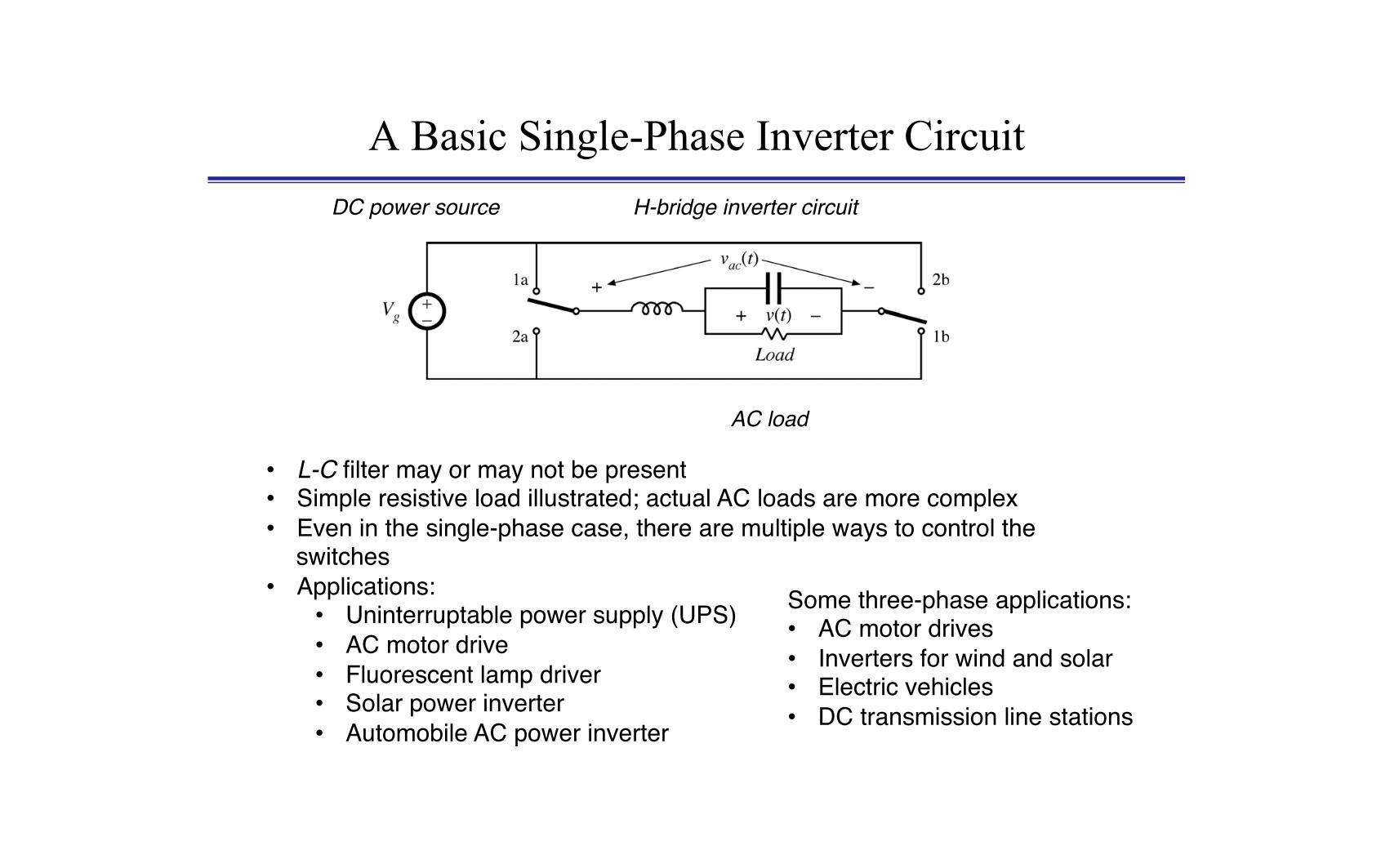
A Basic Single-Phase Inverter Circuit
Power Electronics Lab� 6�
Two ways to generate a PWM sinusoid�
t
vac(t)
(a)� Operate left and right sides with same (complementary) gate drive signals�� �v(t) = (2d(t) – 1) Vg�
(b) �PWM one side, while other side switches at 60 Hz�� �v(t) = ± d(t) Vg�
Two-level waveform�
Three-level waveform�
DC power source
AC load
H-bridge inverter circuit
• L-C filter may or may not be present• Simple resistive load illustrated; actual AC loads are more complex• Even in the single-phase case, there are multiple ways to control the
switches• Applications:
• Uninterruptable power supply (UPS)• AC motor drive• Fluorescent lamp driver• Solar power inverter• Automobile AC power inverter
Some three-phase applications:• AC motor drives• Inverters for wind and solar• Electric vehicles• DC transmission line stations

The “Modified Sine Wave” Inverter
Power Electronics Lab� 4�
“Modified Sine-Wave” Inverter�
vac(t) has a rectangular waveform�
Inverter transistors switch at 60 Hz, T = 8.33 msec�
T/2
DT/2+ V
HVDC
– VHVDC
vac
(t)
RMS value of vac(t) is:�
����� ���
�� ��
�
�
� � ������
•� Choose VHVDC larger than desired Vac,RMS�
•� Can regulate value of Vac,RMS by variation of D�
•� Waveform is highly nonsinusoidal, with significant harmonics�
H-bridge switches at the output frequency• Waveform is highly
nonsinusoidal, with significant harmonics
• Some ac loads can tolerate this waveform, others cannot
• Inexpensive, efficient
Control of ac rms voltage by control of duty cycle D:
Power Electronics Lab� 4�
“Modified Sine-Wave” Inverter�
vac(t) has a rectangular waveform�
Inverter transistors switch at 60 Hz, T = 8.33 msec�
T/2
DT/2+ V
HVDC
– VHVDC
vac
(t)
RMS value of vac(t) is:�
����� ���
�� ��
�
�
� � ������
•� Choose VHVDC larger than desired Vac,RMS�
•� Can regulate value of Vac,RMS by variation of D�
•� Waveform is highly nonsinusoidal, with significant harmonics�
Standalone inverter: inverter drives a passive load, and regulates the voltage supplied to the load
The “True Sine Wave” Inverter
Power Electronics Lab� 6�
Two ways to generate a PWM sinusoid�
t
vac(t)
(a)� Operate left and right sides with same (complementary) gate drive signals�� �v(t) = (2d(t) – 1) Vg�
(b) �PWM one side, while other side switches at 60 Hz�� �v(t) = ± d(t) Vg�
Two-level waveform�
Three-level waveform�Power Electronics Lab� 6�
Two ways to generate a PWM sinusoid�
t
vac(t)
(a)� Operate left and right sides with same (complementary) gate drive signals�� �v(t) = (2d(t) – 1) Vg�
(b) �PWM one side, while other side switches at 60 Hz�� �v(t) = ± d(t) Vg�
Two-level waveform�
Three-level waveform�Power Electronics Lab� 6�
Two ways to generate a PWM sinusoid�
t
vac(t)
(a)� Operate left and right sides with same (complementary) gate drive signals�� �v(t) = (2d(t) – 1) Vg�
(b) �PWM one side, while other side switches at 60 Hz�� �v(t) = ± d(t) Vg�
Two-level waveform�
Three-level waveform�Power Electronics Lab� 6�
Two ways to generate a PWM sinusoid�
t
vac(t)
(a)� Operate left and right sides with same (complementary) gate drive signals�� �v(t) = (2d(t) – 1) Vg�
(b) �PWM one side, while other side switches at 60 Hz�� �v(t) = ± d(t) Vg�
Two-level waveform�
Three-level waveform�Power Electronics Lab� 6�
Two ways to generate a PWM sinusoid�
t
vac(t)
(a)� Operate left and right sides with same (complementary) gate drive signals�� �v(t) = (2d(t) – 1) Vg�
(b) �PWM one side, while other side switches at 60 Hz�� �v(t) = ± d(t) Vg�
Two-level waveform�
Three-level waveform�
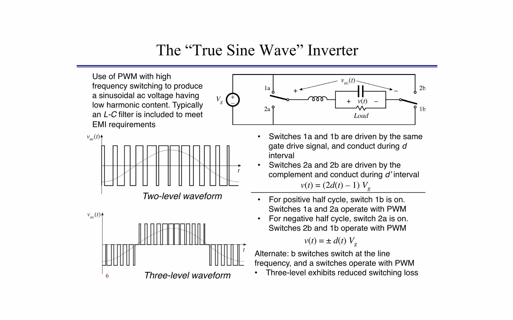
• Switches 1a and 1b are driven by the same gate drive signal, and conduct during d interval
• Switches 2a and 2b are driven by the complement and conduct during d’ interval
• For positive half cycle, switch 1b is on. Switches 1a and 2a operate with PWM
• For negative half cycle, switch 2a is on. Switches 2b and 1b operate with PWM
Alternate: b switches switch at the line frequency, and a switches operate with PWM• Three-level exhibits reduced switching loss
Use of PWM with high frequency switching to produce a sinusoidal ac voltage having low harmonic content. Typically an L-C filter is included to meet EMI requirements
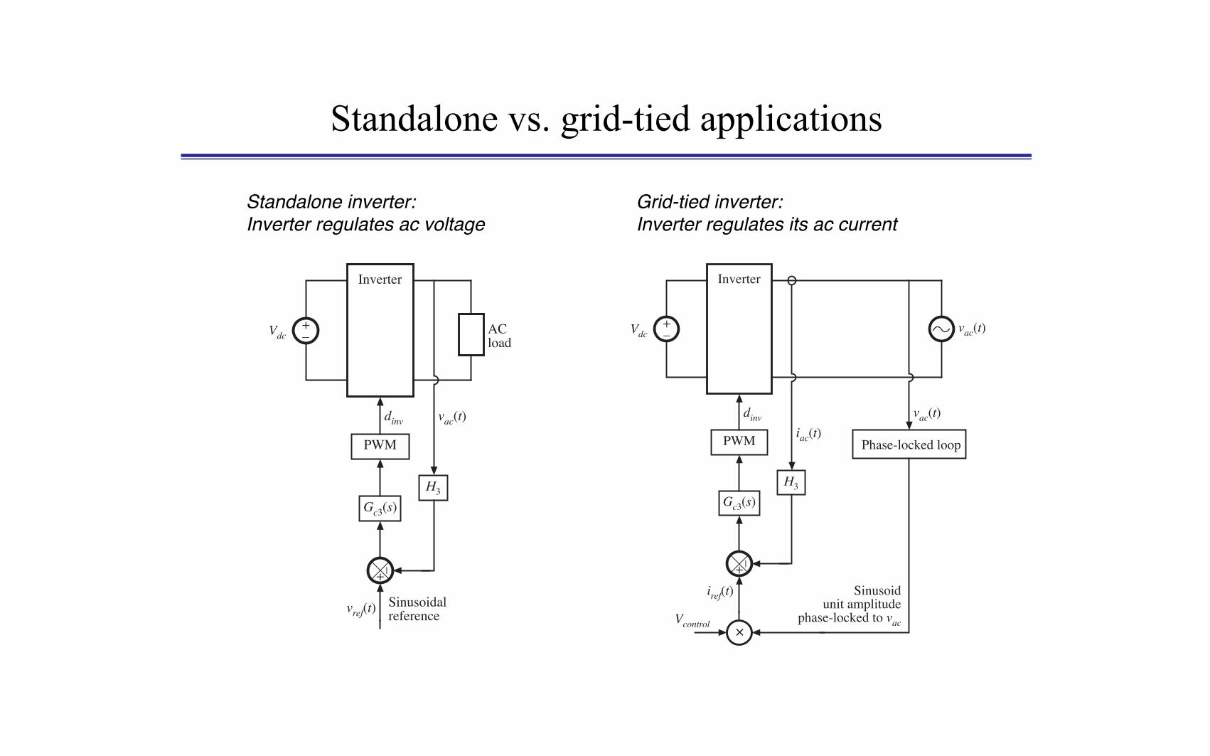
Standalone vs. grid-tied applications
Inverter
vac(t)
dinv
×
iref(t)
Phase-locked loop
vac(t)
PWM
+ –
Sinusoidunit amplitude
phase-locked to vac
H3
iac(t)
Gc3(s)
Vcontrol
+–Vdc
Inverter
dinv
vref(t)
vac(t)
PWM
+ –
H3Gc3(s)
+–Vdc AC
load
Sinusoidalreference
Standalone inverter:Inverter regulates ac voltage
Grid-tied inverter:Inverter regulates its ac current
Reactive power
For a standalone application, the inverter must be capable of supplying whatever current waveform is demanded by the ac load
• Reactive load, in which current is phase-shifted relative to voltage• Distorted current
In most grid-tied applications, the inverter supplies a low-THD current waveform to the grid, with power factor very close to unity.
• Improved efficiency• This opens the possibility of simpler converter topologies using single-
quadrant switches
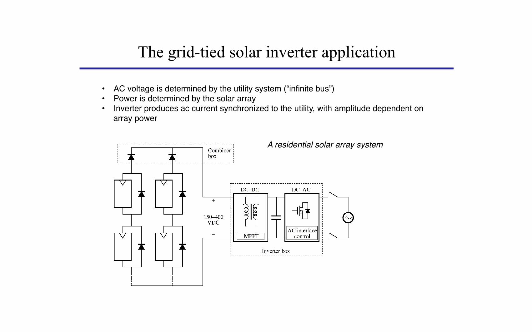
The grid-tied solar inverter application
• AC voltage is determined by the utility system (“infinite bus”)• Power is determined by the solar array• Inverter produces ac current synchronized to the utility, with amplitude dependent on
array power
A residential solar array system
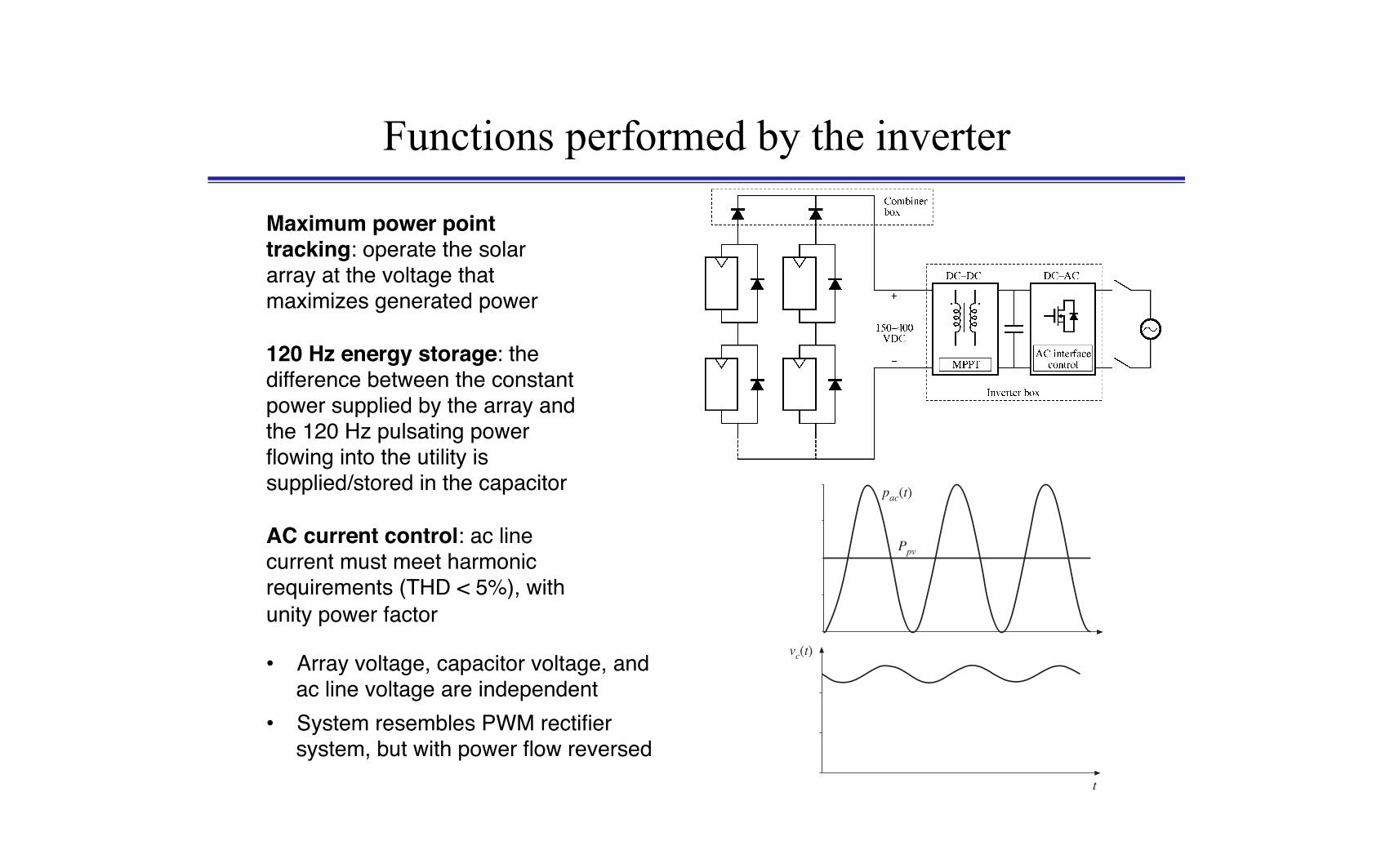
Functions performed by the inverter
Maximum power point tracking: operate the solar array at the voltage that maximizes generated power
120 Hz energy storage: the difference between the constant power supplied by the array and the 120 Hz pulsating power flowing into the utility is supplied/stored in the capacitor
AC current control: ac line current must meet harmonic requirements (THD < 5%), with unity power factor
• Array voltage, capacitor voltage, and ac line voltage are independent
• System resembles PWM rectifier system, but with power flow reversed
Ppv
pac(t)
t
vc(t)

An Inverter System
DC-DCvbus(t)vpv(t) Inverter EMI
vac(t)
dinv
×
iref(t)
PV
d
H2
H1 Phase-locked loop
vac(t)
PWM
+ –
Sinusoidunit amplitude
phase-locked to vac
H3
iac(t)
+–
Gc3(s)
Gc2(s)Vref-bus
ibus
PWM
Gc3(s)
+–
MPPT
Vref-pv
vbus(t)
vpv(t)

Standards
IEEE 1547: standard for connecting a renewable energy source to the utility grid• Current harmonic limit (THD < 5%)• Anti-islanding (detect loss of grid, shut down within 1 sec)• Disconnection when grid frequency or grid voltage is out of bounds
National Electric CodeUL 1741
Weighted Efficiency standards: California Energy Commission (CEC)
Power level, % of rated
Weight
100% 0.05
75% 0.53
50% 0.21
30% 0.12
20% 0.05
10% 0.04
• Provides a way to compare products of different companies
• Weightings reflect typical distribution of array power experienced in California
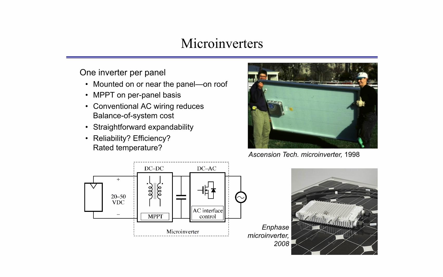
Microinverters
One inverter per panel • Mounted on or near the panel—on roof • MPPT on per-panel basis • Conventional AC wiring reduces
Balance-of-system cost • Straightforward expandability • Reliability? Efficiency?
Rated temperature?
Enphase microinverter,
2008
Ascension Tech. microinverter, 1998
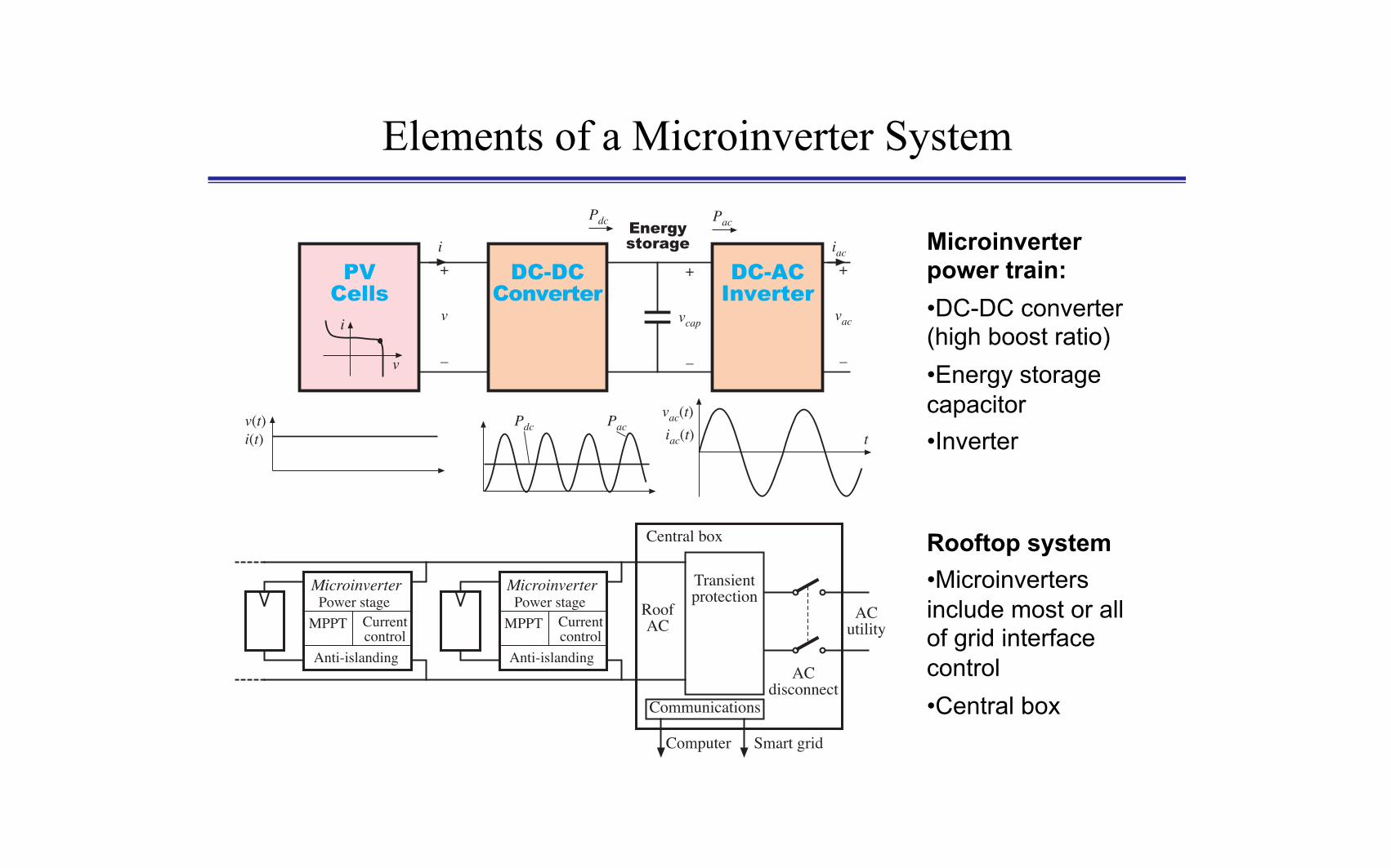
Elements of a Microinverter System
ACutility
Transientprotection
ACdisconnect
Communications
Smart gridComputer
Central box
RoofAC
Microinverter
Power stage
MPPT Currentcontrol
Anti-islanding
Microinverter
Power stage
MPPT Currentcontrol
Anti-islanding
DC-ACInverter
DC-DCConverter
v(t)
i(t)
PVCells
Energystorage
+
vac
–
iac
PacPdc
iac(t) t
vac(t)
+
v
–
i
i
v
PacPdc
+
vcap
–
Microinverter power train: • DC-DC converter (high boost ratio) • Energy storage capacitor • Inverter
Rooftop system • Microinverters include most or all of grid interface control • Central box
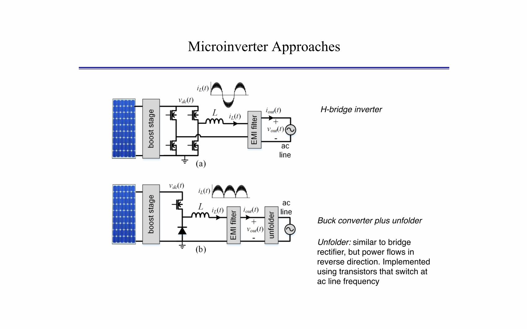
Microinverter Approaches
enables efficient design of the inductor. We also introduce a fast and stable cycle-by-cycle controller that does not
require sensing of the average output current, and thus avoids an expensive current sensor. Overall, the proposed
method enables a low-cost design that operates with a small inductor and achieves a peak efficiency of 99.5 % and a
weighted efficiency of 99.15 %.
II. VARIABLE FREQUENCY PEAK CURRENT CONTROLLER
In this section we present the constant peak current switching scheme. This new scheme is derived through an
analysis of weighted losses in BCM, an analysis that demonstrates that the dominant loss for BCM is switching loss.
To improve the weighted efficiency, we explore which peak current is optimal at each output power, and show that in
DCM the optimal peak current is constant.
A common topology for micro-inverters is the two-stage topology [22], [23], which includes a boost stage and an
inverter stage, as shown in Fig. 1. Typically the boost stage tracks the maximum power point of the PV source, and
boosts the low PV input voltage to a higher voltage. The inverter stage generates the AC current that is injected to the
AC line. Despite various new topologies that have been demonstrated in recent literature [5], the typical low-cost
micro-inverter is still designed either as a full-bridge stage, or as a buck stage with an unfolder stage. The unfolder
stage, if present, switches at the zero-crossings of the line voltage to convert the rectified sinusoid at the buck output
to a full sinusoid on the AC line.
Fig. 1. Common micro-inverter power stages. (a) Full bridge. (b) Buck stage with an unfolder stage.
An illustration of the Boundary Conduction Mode (BCM) waveform is shown in Fig. 2. Although it is soft-
switching, and operates with low RMS current, a disadvantage of BCM is its high average switching frequency, which
causes high switching losses. As demonstrated by equation (1), the BCM waveform has the highest switching
frequency among all DCM waveforms. This is because the peak current of BCM is equal to ipk(t)=2iout(t), which is the
H-bridge inverter
Buck converter plus unfolder
Unfolder: similar to bridge rectifier, but power flows in reverse direction. Implemented using transistors that switch at ac line frequency
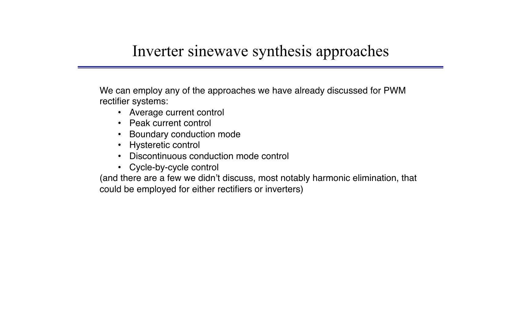
Inverter sinewave synthesis approaches
We can employ any of the approaches we have already discussed for PWM rectifier systems:
• Average current control• Peak current control• Boundary conduction mode• Hysteretic control• Discontinuous conduction mode control• Cycle-by-cycle control
(and there are a few we didn’t discuss, most notably harmonic elimination, that could be employed for either rectifiers or inverters)

Synthesizing a Sinusoidal Current: Boundary Conduction Mode (BCM)
lowest possible peak current in DCM, and as a result the switching frequency in BCM is maximal. Equation (1) also
predicts that the switching frequency of BCM increases at low output powers, creating a switching frequency profile
that causes disproportional switching losses at low powers. This is demonstrated by the last expression in equation (1)
for which the power-factor is unity and the switching frequency is proportional to Rout. A lower output voltage vout(t)
results in a higher switching frequency, so the switching frequency and switching losses in BCM substantially increase
at low voltages and low powers.
Fig. 2. Illustration of the inductor current in BCM, showing soft switching transitions (ZVS, ZCS) and the variations in switching
frequency over the line cycle.
The switching frequencies in DCM and BCM are given by:
� � � �� �
� �� �
� �� �
� � � �� �
� �� �
� � � �� �
� �� �
22
DCM: 12
BCM: 12
BCM with unity power factor :
1 ,where2
out out outs
out dc pk
out outs
out dc
out outouts out
dc out
v t v t i tf t
L i t v t i t
v t v tf t
L i t v t
v t v tRf t RL v t i t
§ ·§ · � ¨ ¸¨ ¸¨ ¸¨ ¸� © ¹© ¹
§ · �¨ ¸¨ ¸� © ¹
§ · � ¨ ¸¨ ¸
© ¹
(1)
Fig. 3 shows how the total loss in BCM distributes at various output powers. The losses in this figure are averaged
over a line cycle, and are shown in percent relative to the cycle averaged output power. The total loss is composed of
four types of loss: conduction losses, switching losses, proximity loss in the inductor, and core loss in the inductor.
The losses are computed according to the calibrated loss model presented in Section IV. The conditions for the test
are AC voltage of 220 Vrms @ 60 Hz, average AC power of 300 W, bus voltage of 425 V, and an inductor of 300 µH
built on a PQ 26/20 core. The results demonstrate that the dominant loss mechanism in BCM at low powers is
switching loss.
Inductor current waveform, BCM
Fig. 3. Distribution of losses in BCM. The vertical bars represent average losses over an AC line cycle. The losses are shown in percent
relative to the average AC output power. Switching losses dominate at low powers.
This data in Fig. 3 suggests that the weighted efficiency of BCM may be substantially improved if the low power
switching losses are reduced. According to equation (1), this may be achieved by increasing the peak current. To
demonstrate this idea, Fig. 4 compares a BCM waveform and a DCM waveform with a higher peak current. Although
both waveforms provide the same average current (iout), the DCM waveform delivers more energy to the output at
every cycle, and as a result operates with a lower switching frequency that enables lower switching losses.
Thus, to achieve a certain average current, the controller can vary either the peak current or the switching frequency
of the inductor current waveform. A higher peak current reduces the switching frequency, but also raises the RMS
current and causes more conduction losses. At each operating point, there is an optimal peak current that minimizes
the sum of these losses. To discover which peak current is optimal, Fig. 5 shows a plot of efficiency as a function of
peak current (ipk) at various DC operating points. Each curve in this figure corresponds to one DC operating point,
with fixed average current and voltage (iout and vout). The minimal ipk at every curve is 2iout, which corresponds to a
BCM waveform. The DC operating points are selected with constant ratio of voltage and current vout/iout = Rout, and
thus reside on the same output sinusoid. The efficiency is computed according to the calibrated loss model presented
in section IV, with conditions as follows: Rout = 215.1 Ω, average AC power of 225 W, bus voltage of vbus = 425 V,
and an inductor of 300µH built on a PQ 26/20 core. Each curve is label by its output power pout = voutiout, which is
given in percent relative to the maximal instantaneous output power of 450 W.
Fig. 4. By increasing the peak current in DCM, the switching frequency is reduced, while the average inductor current (iout) is unchanged.
Loss components at different solar irradiance levels, BCM(300 W, 240 Vac example)
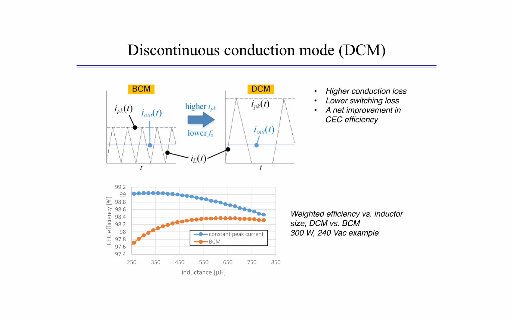
Discontinuous conduction mode (DCM)
Fig. 3. Distribution of losses in BCM. The vertical bars represent average losses over an AC line cycle. The losses are shown in percent
relative to the average AC output power. Switching losses dominate at low powers.
This data in Fig. 3 suggests that the weighted efficiency of BCM may be substantially improved if the low power
switching losses are reduced. According to equation (1), this may be achieved by increasing the peak current. To
demonstrate this idea, Fig. 4 compares a BCM waveform and a DCM waveform with a higher peak current. Although
both waveforms provide the same average current (iout), the DCM waveform delivers more energy to the output at
every cycle, and as a result operates with a lower switching frequency that enables lower switching losses.
Thus, to achieve a certain average current, the controller can vary either the peak current or the switching frequency
of the inductor current waveform. A higher peak current reduces the switching frequency, but also raises the RMS
current and causes more conduction losses. At each operating point, there is an optimal peak current that minimizes
the sum of these losses. To discover which peak current is optimal, Fig. 5 shows a plot of efficiency as a function of
peak current (ipk) at various DC operating points. Each curve in this figure corresponds to one DC operating point,
with fixed average current and voltage (iout and vout). The minimal ipk at every curve is 2iout, which corresponds to a
BCM waveform. The DC operating points are selected with constant ratio of voltage and current vout/iout = Rout, and
thus reside on the same output sinusoid. The efficiency is computed according to the calibrated loss model presented
in section IV, with conditions as follows: Rout = 215.1 Ω, average AC power of 225 W, bus voltage of vbus = 425 V,
and an inductor of 300µH built on a PQ 26/20 core. Each curve is label by its output power pout = voutiout, which is
given in percent relative to the maximal instantaneous output power of 450 W.
Fig. 4. By increasing the peak current in DCM, the switching frequency is reduced, while the average inductor current (iout) is unchanged.
• Higher conduction loss• Lower switching loss• A net improvement in
CEC efficiency
To find the optimal values of the inductance L and magnetic flux density ΔBmax, we used a computer program that
numerically scanned the weighted efficiency of every combination of these two parameters. The program runs over
each output power level, and over single DC operating points in the output sinusoid, and computes the efficiency at
each operating point, using the calibrated loss model. The resulting efficiency data is averaged according to the CEC
efficiency formula (see section V). Typical results of this simulation are shown in Fig. 10, for a PQ 26/20 magnetic
core, and conditions as detailed in Table I.
Fig. 10. Weighted CEC efficiency with a PQ 26/20 magnetic core, for a BCM controller and the proposed constant peak current
controller.
Fig. 10 shows the optimal inductance values (L) for the BCM control method, and for the proposed constant peak
current method. These optimal inductance values achieve the best mix of frequency dependent losses and Ohmic
losses. Notice that a higher inductance value in Fig. 10 does not mean a larger inductor, because the magnetic core is
the same (PQ26/20) at all the data points. Nevertheless, the optimal inductance value in BCM is considerably higher
in comparison to the optimal value of the constant current controller. The reason for this difference is that a higher
inductance is needed in BCM, to reduce the otherwise high switching frequencies that occur with this control method.
The higher inductance requires more turns of wire on the inductor core, which is one reason why BCM is less efficient
in comparison to the proposed constant peak current controller.
97.497.697.8
9898.298.498.698.8
9999.2
250 350 450 550 650 750 850
CEC
effic
ienc
y [%
]
inductance [µH]
constant peak currentBCM
Weighted efficiency vs. inductor size, DCM vs. BCM300 W, 240 Vac example
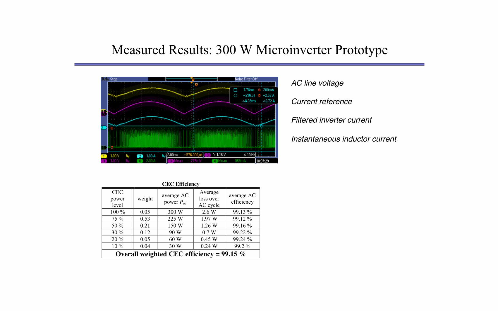
Measured Results: 300 W Microinverter Prototype
The current sense resistor is located between the FET source and ground, and senses the rising slope of the inductor
current. The only function of this sensed signal is to turn off the FET when the inductor current reaches the designated
peak current Ipk. The voltage sensor is implemented by a comparator that connects to an auxiliary winding (3 turns)
on the inductor. Its purpose is to detect the moment in which the inductor current reaches zero, the moment in which
the cycle-by-cycle integrator voltage starts to discharge (See Fig. 8). As explained in Section IV, at this moment the
switching node voltage starts oscillating, and the voltage across the inductor changes polarity. This change is detected
by the comparator, which resets the controller SR flip-flop. The oscillating output of the auxiliary winding comparator
is shown in Fig. 12 (blue waveform). This graph also shows the voltage across the cycle-by-cycle integration capacitor
(vint, yellow waveform). The inverter waveforms over a 60 Hz line cycle are shown in Fig. 13.
Fig. 12. Inverter waveforms at a DC operating point. Ch1 (yellow) cycle-by-cycle integration capacitor voltage vint(t) , Ch2 (blue) auxiliarywinding voltage sensor, at comparator output, Ch4 (green) inductor current iL(t). Conditions: Vdc= 426.8 V, Idc= 0.98 A, vout= 330.1 V, iout=
1.259 A.
Fig. 13. Inverter waveforms over a line cycle. Ch1 (yellow) AC line voltage sensor, Ch2 (blue) AC current iac(t), Ch3 (magenta) referencesignal iref(t), Ch4 (green) inductor current iL(t). Conditions: Vdc= 425 V, Idc= 0.462 A, Rload=253 Ω
The efficiency of the inverter is measured at static DC operating points. These tests are done with a power supply
at the input and a variable load resistor (Rload) at the output. To increase the accuracy of the measurements, the meters
at the input and output are filtered by large EMI inductors. The efficiency results are shown in Fig. 14. The various
curves in the figure correspond to tests with different average AC powers (Pac). At each such test the load resistor is
set to Rload=Vac,rms2/Pac, and the instantaneous output power is scanned in the range 0 … 2Pac.
Fig. 14. Efficiency measurements at DC operating points, for various average AC powers
At each power level, the AC efficiency is computed by averaging the DC efficiencies over a line cycle. The results
are again averaged by the CEC weighted average formula to obtain the overall CEC efficiency. The AC efficiency is
computed by equation (9), and the results are summarized in Table II.
� �
� �� �� �
� � � �
/
20/
0
AC efficiency where sin
ac
ac
out
AC out ac acout
DC out
p t dtp t P t
p tdt
p t
S Z
S ZK Z
K
³
³(9)
In this equation, Pac is the average AC power, pout(t) is the output power at a DC operating point, and ηDC(pout) is the
efficiency at those operating points, as shown in Fig. 14. The weighted CEC efficiency is found to be 99.15 %.
TABLE II CEC Efficiency
CEC power level
weight average AC power Pac
Average loss over AC cycle
average ACefficiency
100 % 0.05 300 W 2.6 W 99.13 % 75 % 0.53 225 W 1.97 W 99.12 % 50 % 0.21 150 W 1.26 W 99.16 % 30 % 0.12 90 W 0.7 W 99.22 % 20 % 0.05 60 W 0.45 W 99.24 % 10 % 0.04 30 W 0.24 W 99.2 %
Overall weighted CEC efficiency = 99.15 %
97
97.5
98
98.5
99
99.5
100
0 200 400 600
effic
ienc
y [%
]
DC output power pout [W]
300 W 225 W150 W 90 w60 W
AC line voltage
Current reference
Filtered inverter current
Instantaneous inductor current
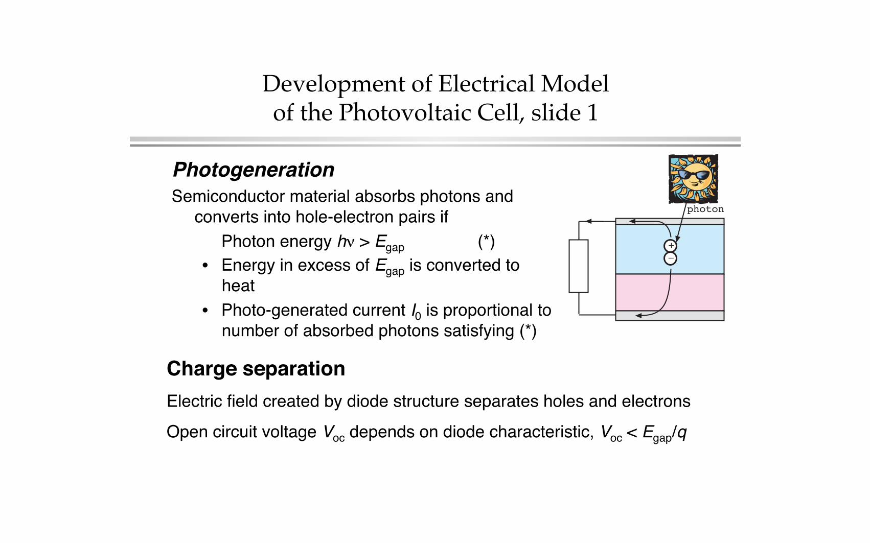
Development of Electrical Modelof the Photovoltaic Cell, slide 1�
Photogeneration�
Semiconductor material absorbs photons and converts into hole-electron pairs if�
�Photon energy h� > Egap � �(*)�
•� Energy in excess of Egap is converted toheat�
•� Photo-generated current I0 is proportional to number of absorbed photons satisfying (*)�
photon
+
–
Charge separation�
Electric field created by diode structure separates holes and electrons�
Open circuit voltage Voc depends on diode characteristic, Voc < Egap/q�

Development of Electrical Modelof the Photovoltaic Cell, slide 2�
Current source I0 models photo-generated current�
I0 is proportional to the solar irradiance, also called the “insolation”:�
�I0 = k (solar irradiance)�
Solar irradiance is measured in W/m^2�
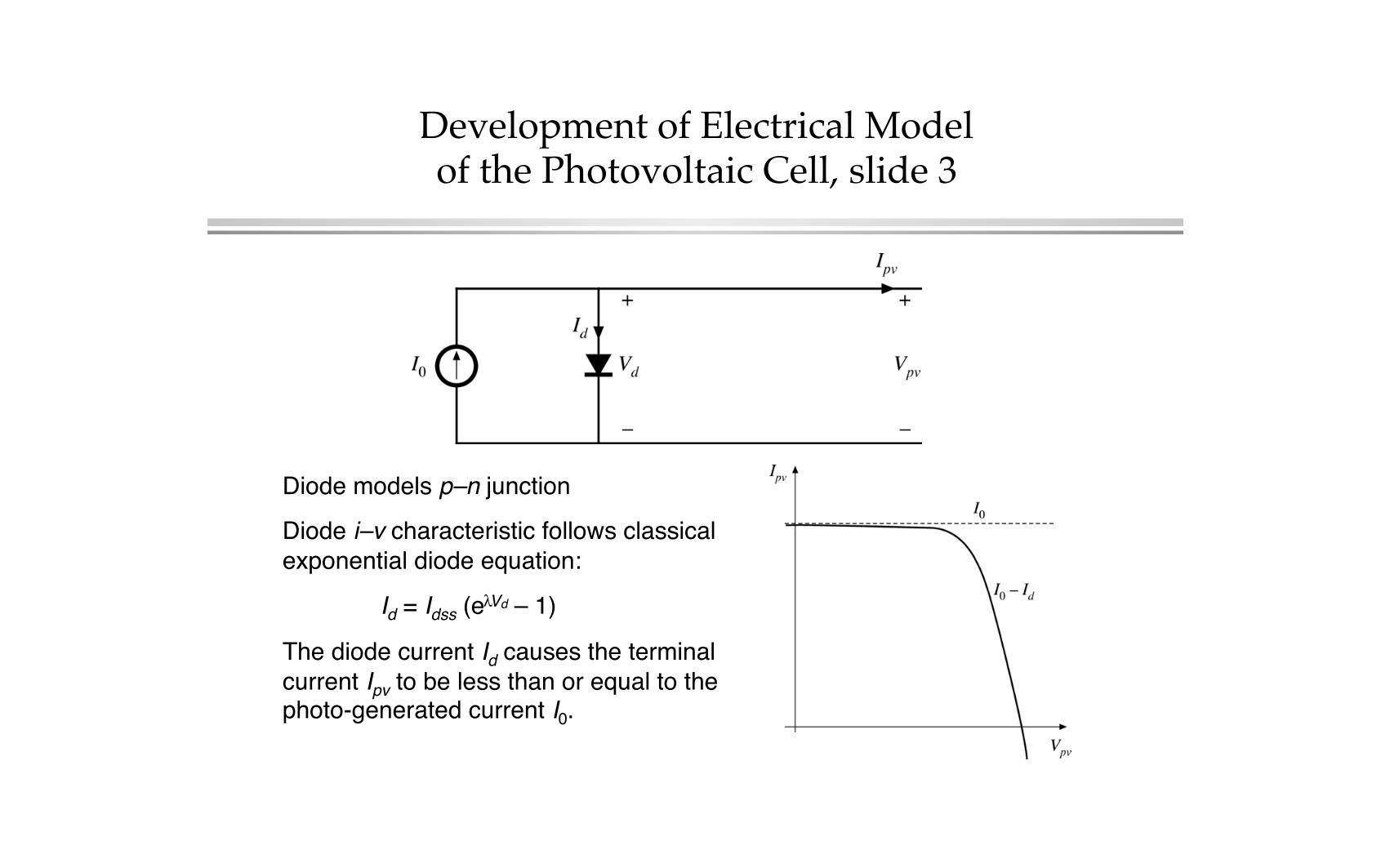
Development of Electrical Modelof the Photovoltaic Cell, slide 3�
Diode models p–n junction�
Diode i–v characteristic follows classical exponential diode equation:�
�Id = Idss (e Vd – 1)�
The diode current Id causes the terminal current Ipv to be less than or equal to the photo-generated current I0.�

Development of Electrical Modelof the Photovoltaic Cell, slide 4�
Modeling nonidealities:�
R1 : defects and other leakage current mechanisms�
R2 : contact resistance and other series resistances�
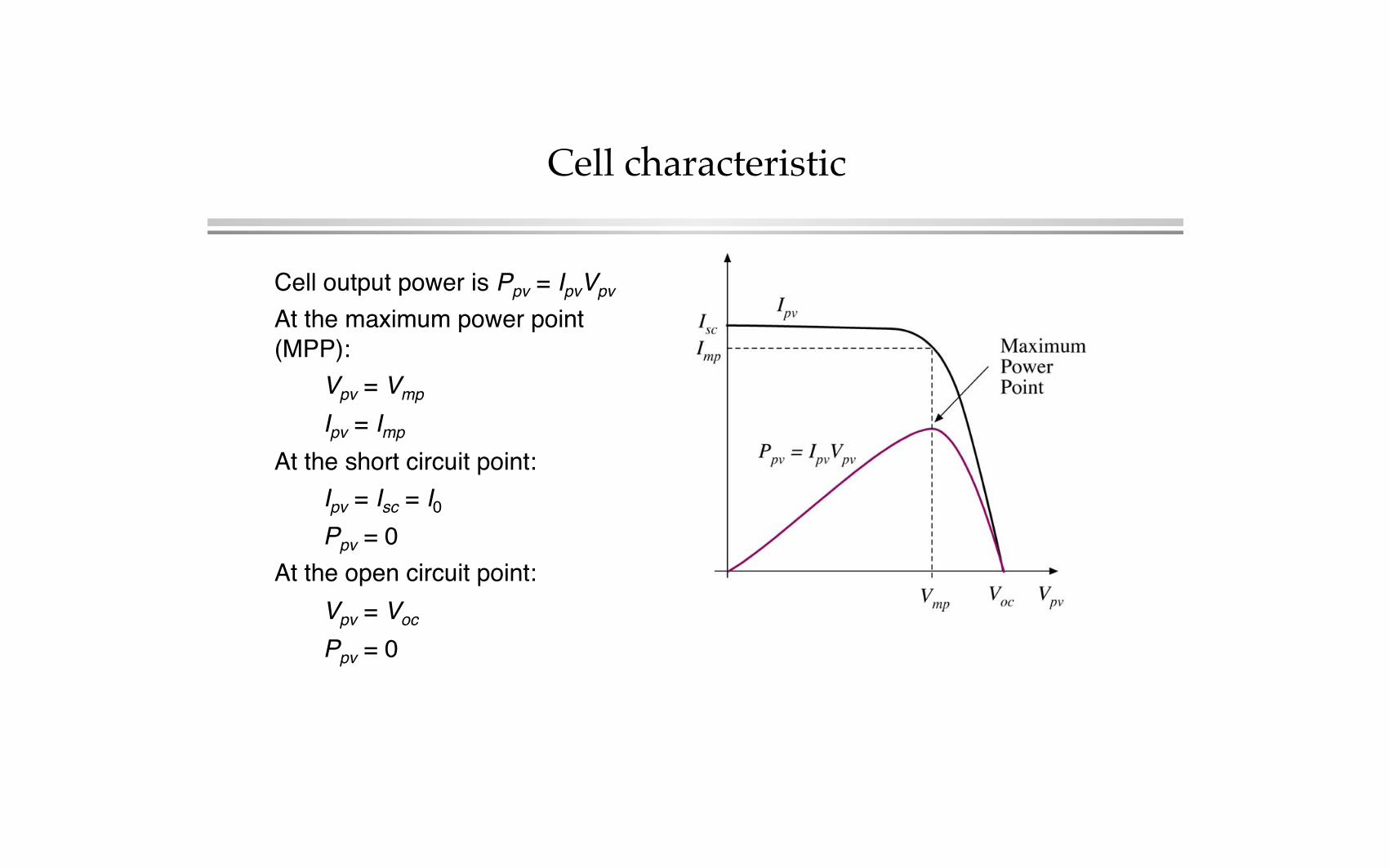
Cell characteristic�
Cell output power is Ppv = IpvVpv�At the maximum power point (MPP):�
Vpv = Vmp�Ipv = Imp�
At the short circuit point:�Ipv = Isc = I0�Ppv = 0�
At the open circuit point:�Vpv = Voc�Ppv = 0�

Maximum Power Point Tracking�
Automatically operate the PV panel at its maximum power point�
I-V curve with partial shading
Power vs. voltage
Some possible MPPT algorithms:
• Perturb and observe
• Periodic scan
• Newton s method, or related hill-climbing algorithms
• What is the control variable? Where is the power measured?
!
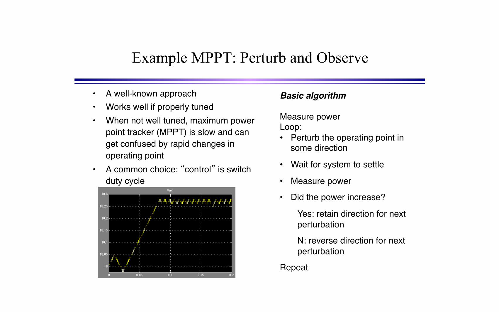
Example MPPT: Perturb and Observe • A well-known approach"• Works well if properly tuned"• When not well tuned, maximum power
point tracker (MPPT) is slow and canget confused by rapid changes inoperating point"
• A common choice: �control� is switchduty cycle"
Basic algorithm!!Measure power"Loop:"• Perturb the operating point in
some direction"
• Wait for system to settle"
• Measure power"
• Did the power increase?"
Yes: retain direction for next perturbation"
N: reverse direction for next perturbation"
Repeat"
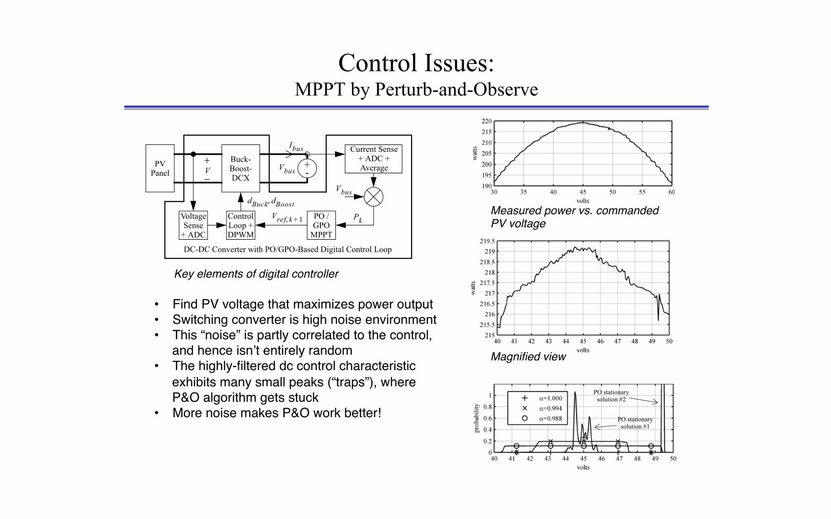
Control Issues: MPPT by Perturb-and-Observe
����)!' �
/�&� **-.�
�*'.�#!�!)-!�����
�*).,*'�**+������
�����������
��� ��,
�����
��� �/,,!).��!)-!�������
���
�
�0!,�#!���
�������*)0!,.!,�1%.$�������� �-! ��%#%.�'��*).,*'��**+
���� ���� �,
Key elements of digital controller�
Measured power vs. commanded PV voltage�
Magnified view�
• Find PV voltage that maximizes power output• Switching converter is high noise environment• This “noise” is partly correlated to the control,
and hence isn’t entirely random• The highly-filtered dc control characteristic
exhibits many small peaks (“traps”), whereP&O algorithm gets stuck
• More noise makes P&O work better! ��� �������� ��������
��� �������� ��������
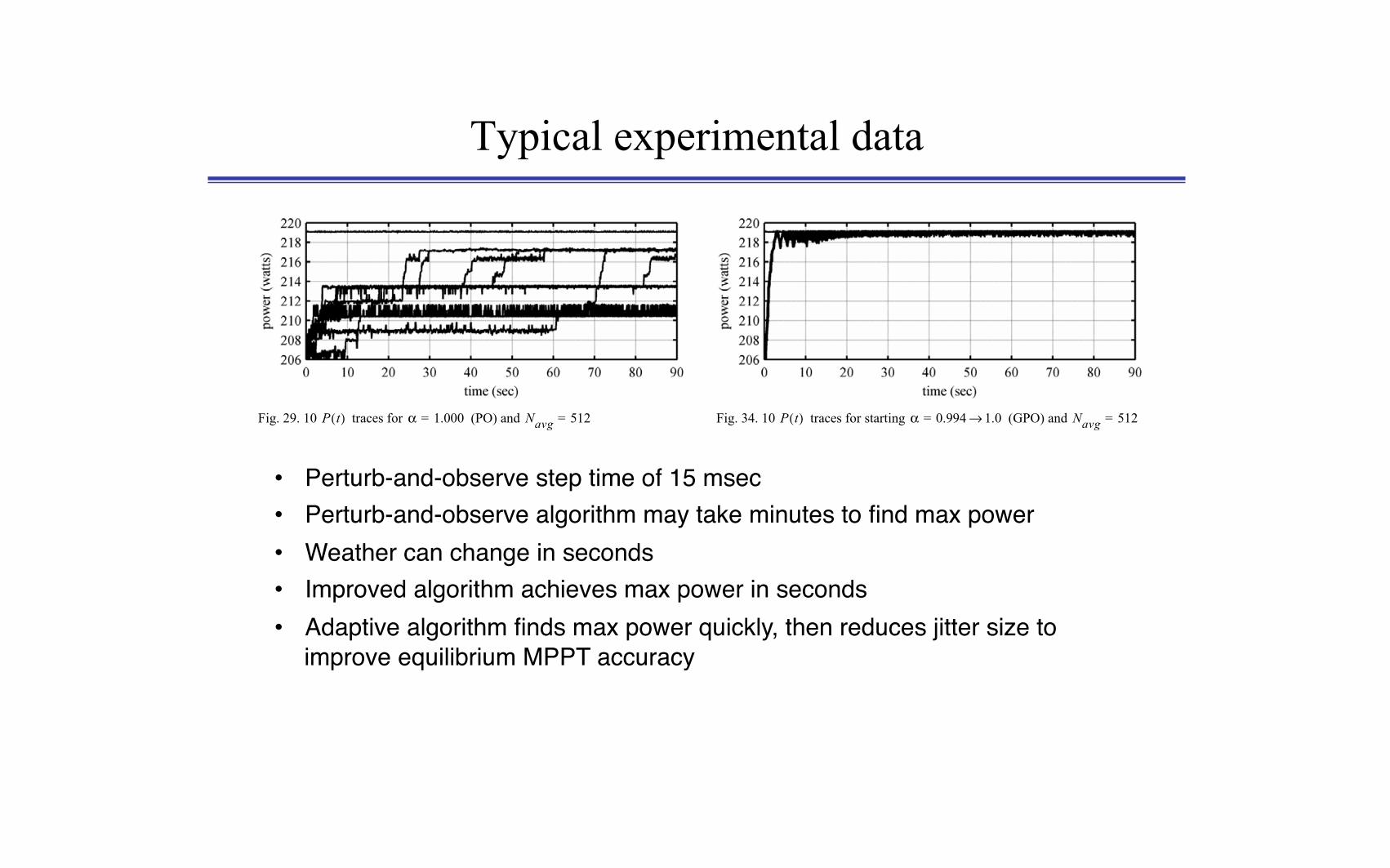
Typical experimental data
����������� ������������ ����������� �( ) α ������ ���� ��� ���������� ��������������������� ������������ �( ) α ���� ���→� ���� ���
• Perturb-and-observe step time of 15 msec• Perturb-and-observe algorithm may take minutes to find max power• Weather can change in seconds• Improved algorithm achieves max power in seconds• Adaptive algorithm finds max power quickly, then reduces jitter size to
improve equilibrium MPPT accuracy