semiconductor metrology applications - bruker · 2013-01-31 · semiconductor metrology...
TRANSCRIPT

Semiconductor Metrology ApplicationsContourGT-X Platform Capabilities and Automation for Semiconductor Applications

BRUKER CONFIDENTIAL
Outline
• Introduction
• Brief BNS – SOM General Overview
• Semiconductor Applications
• Automation Cassette/Wafer Loading
• Summary and Questions

BRUKER CONFIDENTIAL
Bruker Stylus and Optical MetrologySOM - World Leading Surface Metrology
• History of QA/QC solutions for industry Semiconductor
100+ Installed base multi-chip module inspection at board level
Data Storage 500+ Installed base disk drive slider metrology
Electronics and Industrial1000+ Installed base
Worldwide10,000+ Installed base
• Manufacturing Excellence Lean, six sigma-based process
100+ systems/quarter capacity
Rapid production ramp capability
1/30/2013 3
New Facility - Tucson, Arizona, USA Opened December 2011

BRUKER CONFIDENTIAL
3D Microscope Surface MetrologyGeneral Benefits of Core Technology
• Fast, accurate, GR&R capable metrology
• Non-contact, non-destructive
• 1000+ analysis parameters
• Stable and operator independent data
1/30/2013 4

BRUKER CONFIDENTIAL
Bruker Stylus and Optical MetrologyOur Products Broad Overview
1/30/2013 5
DektakXTContourGT-K
ContourGT-IM
ContourGT-XNPFLEX
NPFLEX-LA
SP9900+
ContourGT Auto-Ready
BRUKER CONFIDENTIAL
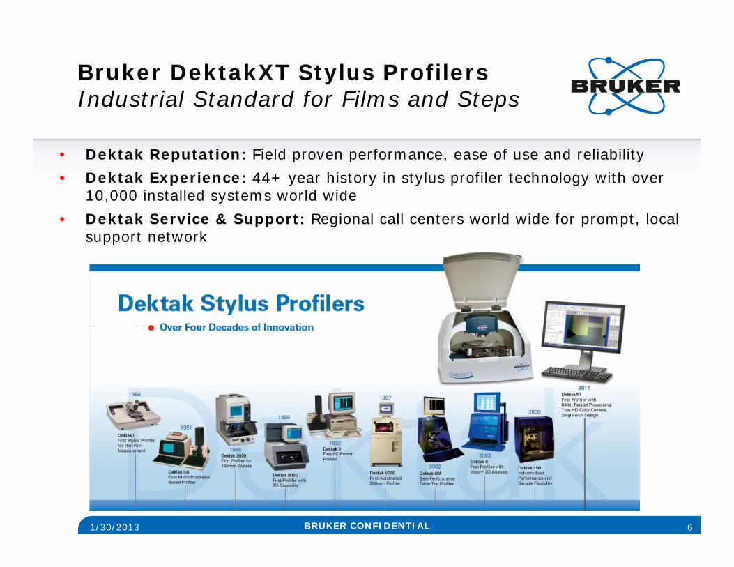
Bruker DektakXT Stylus ProfilersIndustrial Standard for Films and Steps
1/30/2013 6
• Dektak Reputation: Field proven performance, ease of use and reliability• Dektak Experience: 44+ year history in stylus profiler technology with over
10,000 installed systems world wide• Dektak Service & Support: Regional call centers world wide for prompt, local
support network

BRUKER CONFIDENTIAL
ContourGT-X Platform DetailStable, Accurate, Automation Ready
• Optical Metrology Module (OMM) with self-calibration on X8
• Programmable 8” or 12” Stage
• Automated Tip-Tilt in the head (+/- 6 degrees)
• Automated Z-Axis Focus
• Single Objective Adapter up to 5 -Position Automated Turret
• Dell Multi-Core PC Running Windows 7, 64 Bit Platform
• Vision64 Operation Software – advanced
• Single 23” Monitor with 1920x1080 resolution
• Operator Assist Sample Lamp
• Small Footprint Option with Automation Ready Package
• Integrated Isolation Table
1/30/2013 7

BRUKER CONFIDENTIAL
Focus
WLI measures the intensity at each pixel as the objective is moving vertically and analyzes the intensity while moving through focus to determine the height of the surface at each pixel
3D Optical MicroscopesWLI – Accurate, Fast, GR&R Ready!

BRUKER CONFIDENTIAL
Apply Benefits to Industry ProblemsSemiconductor Applications
• Broad range of applications including
Laser probe mark depth
Sensor dimensions and frequency performance (MEMS, DMEMS)
Cu wire bonding (bond force optimization, near line inspection)
Multichip Module HDI production inspection
Others (see next slides)
9

BRUKER CONFIDENTIAL
Range of Semiconductor Applications
January 30, 2013 Slide 10Bruker ConfidentialStylus and Optical Metrology Unit

BRUKER CONFIDENTIAL
Probe Mark SolutionAuto Detect Deepest Point
January 30, 2013 Slide 11
Auto filter removes higher level from the reference area

BRUKER CONFIDENTIAL
Probe Mark Solution Auto Detect Highest Peak
January 30, 2013 Slide 12
Auto filter removes lower level from the reference
BRUKER CONFIDENTIAL
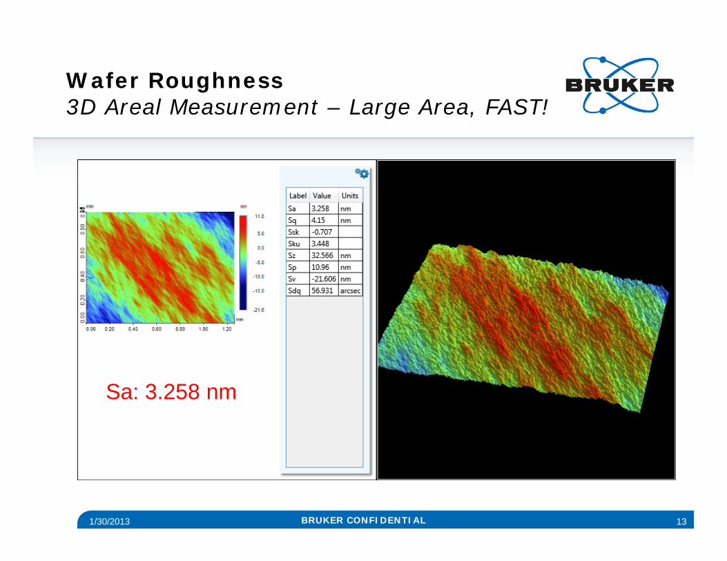
Wafer Roughness 3D Areal Measurement – Large Area, FAST!
1/30/2013 13
Sa: 3.258 nm

BRUKER CONFIDENTIAL
Deposition, Etch, Probe MarksFast, accurate dimensions – non-contact!
1/30/2013 14

BRUKER CONFIDENTIAL
Lead Frame SurfacesRoughness and 3D Areal Parameters

BRUKER CONFIDENTIAL
Roughness and Sdr Uniformity:Lead vs. Die Area – Roughness alone not enough to tell the story
1/30/2013 16
Die B – Sdrdifferent even though Sa is the same

BRUKER CONFIDENTIAL
Die AttachHeight and Tilt Referenced to Lead Frame
1/30/2013 17

BRUKER CONFIDENTIAL
Laser Mark and Bump HeightsAuto detect troughs and peaks
1/30/2013 18
Software auto detects features
of interest –every time!
BRUKER CONFIDENTIAL
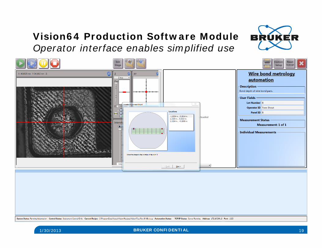
Vision64 Production Software ModuleOperator interface enables simplified use
1/30/2013 19
BRUKER CONFIDENTIAL
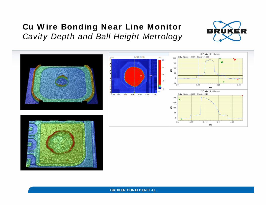
Cu Wire Bonding Near Line MonitorCavity Depth and Ball Height Metrology

BRUKER CONFIDENTIAL
Wire Bond Near Line Monitor3D Optical Microscope >5x Faster than industry standard methodology
40
10
15
0.25
0 10 20 30 40 50 60
SEM
Bruker OpticalProfiler
Sample Preparation (minutes) Measurement / Analysis (minutes)

BRUKER CONFIDENTIAL
Al Pad Metal SplashAuto Detection and Analysis
Splash Analysis
Area of interest is identified by software
Highest peak and volume of Splash
BRUKER CONFIDENTIAL
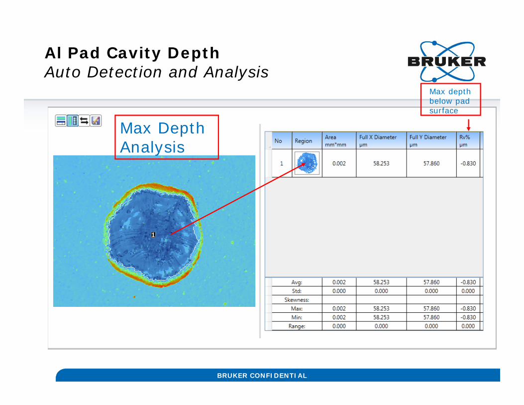
Al Pad Cavity DepthAuto Detection and Analysis
Max Depth Analysis
Max depth below pad surface

BRUKER CONFIDENTIAL
Bruker 3D Optical MicroscopesQuality Characteristics
1/30/2013 24
FAST ACCURATE REPEATABLE

BRUKER CONFIDENTIAL
Vision64 Stage AutomationFast and simple operator setup
• XY Scatter and XY Grid functionality
• Wafer overlays clarify die positions and setup
• Grids are numbered and sub-grid (measure) locations are easily marked
• Variety of traversal patterns offered to customize motion
1/30/2013 25

BRUKER CONFIDENTIAL
Programmable Staging Wafer Grid and Within-Die Variable Points
1/30/2013 26

BRUKER CONFIDENTIAL
Cassette Loading Wafer AutomationContourGT-X Automation Ready Solution
• TCP/IP interface
• Partner with CHAD Industries
• CHAD 200mm, 300mm systems provide front end interface
• SECS standard communication
• Bruker X8 data is transmitted to CHAD system
• Factory MES or SPC system seamlessly interacts with CHAD interface
1/30/2013 27

BRUKER CONFIDENTIAL
Bruker BNS – SOM BUWorldwide Presence - World Class Support
1/30/2013 28
Bruker Corporation
Headquarters
BNS Mfg.Santa
Barbara
BNS Mfg.
Tucson
BNSSingapore
BNSHsinchuBNS
Bangkok
BNSPenang
BNSShanghai
BNSBeijing
BNSPalaiseau
BNSCambridg
e
BNSKarlsruh
e
BNSMalvern
BNS Mfg.Campbell
BNSIndia BNS
Brasil

BRUKER CONFIDENTIAL
2012 2013-2014 2015
System
Functionality
• Broad applications in Semi packaging/MCM
• Partner for auto ready solution
• MEMS/sensor metrology Color camera/defect inspect
• ISO Class 6 compatibility
• ISO Class 2 solution• 450 mm auto loading• Integrated defect
inspection
Throughput• Baseline • 2x improvement via
hardware/computational• 5x over baseline
System S/W and Interface
• Vision64, 64 bit OS• TCP/IP control via
automation client or remote operation
• Streamlined software/GUIintegration
• Enhanced Vision64 functionality
• SECS/GEM with wafer handling
• Simplest, fastest Operator control
• SECS/GEM interfacing via full wafer handling or stand alone systems
Overview of Two Year RoadmapSemiconductor solutions
30.01.2013 29

BRUKER CONFIDENTIAL
SUMMARY
• Overview of product solutions
• Bruker serves a range of customers in the electronics and semiconductor spaces today
• ContourGT-X platform addresses with and without cassette loading several 3D metrology needs
• Automation solution is currently available and Bruker looks forward to serving your growing metrology needs
30

BRUKER CONFIDENTIAL
THANK YOU!!!QUESTIONS?
Bruker Nano Surfaces
[email protected]@bruker-nano.com
www.bruker.com

www.bruker.com
© Copyright Bruker Corporation. All rights reserved.