sensors data sheet tle5012b angle sensor - infineon
TRANSCRIPT

Sensors
Data Sheet V 0.9, 2011-06Preliminary
TLE5012B
Angle SensorGMR-Based Angular Sensor

Edition 2011-06Published byInfineon Technologies AG81726 Munich, Germany© 2011 Infineon Technologies AGAll Rights Reserved.
Legal DisclaimerThe information given in this document shall in no event be regarded as a guarantee of conditions or characteristics. With respect to any examples or hints given herein, any typical values stated herein and/or any information regarding the application of the device, Infineon Technologies hereby disclaims any and all warranties and liabilities of any kind, including without limitation, warranties of non-infringement of intellectual property rights of any third party.
InformationFor further information on technology, delivery terms and conditions and prices, please contact the nearest Infineon Technologies Office (www.infineon.com).
WarningsDue to technical requirements, components may contain dangerous substances. For information on the types in question, please contact the nearest Infineon Technologies Office.Infineon Technologies components may be used in life-support devices or systems only with the express written approval of Infineon Technologies, if a failure of such components can reasonably be expected to cause the failure of that life-support device or system or to affect the safety or effectiveness of that device or system. Life support devices or systems are intended to be implanted in the human body or to support and/or maintain and sustain and/or protect human life. If they fail, it is reasonable to assume that the health of the user or other persons may be endangered.

TLE5012B
Preliminary Data Sheet 3 V 0.9, 2011-06
Trademarks of Infineon Technologies AGAURIX™, BlueMoon™, COMNEON™, C166™, CROSSAVE™, CanPAK™, CIPOS™, CoolMOS™, CoolSET™,CORECONTROL™, DAVE™, EasyPIM™, EconoBRIDGE™, EconoDUAL™, EconoPACK™, EconoPIM™,EiceDRIVER™, EUPEC™, FCOS™, HITFET™, HybridPACK™, ISOFACE™, I²RF™, IsoPACK™, MIPAQ™,ModSTACK™, my-d™, NovalithIC™, OmniTune™, OptiMOS™, ORIGA™, PROFET™, PRO-SIL™,PRIMARION™, PrimePACK™, RASIC™, ReverSave™, SatRIC™, SIEGET™, SINDRION™, SMARTi™,SmartLEWIS™, TEMPFET™, thinQ!™, TriCore™, TRENCHSTOP™, X-GOLD™, XMM™, X-PMU™,XPOSYS™.
Other TrademarksAdvance Design System™ (ADS) of Agilent Technologies, AMBA™, ARM™, MULTI-ICE™, PRIMECELL™,REALVIEW™, THUMB™ of ARM Limited, UK. AUTOSAR™ is licensed by AUTOSAR development partnership.Bluetooth™ of Bluetooth SIG Inc. CAT-iq™ of DECT Forum. COLOSSUS™, FirstGPS™ of Trimble NavigationLtd. EMV™ of EMVCo, LLC (Visa Holdings Inc.). EPCOS™ of Epcos AG. FLEXGO™ of Microsoft Corporation.FlexRay™ is licensed by FlexRay Consortium. HYPERTERMINAL™ of Hilgraeve Incorporated. IEC™ ofCommission Electrotechnique Internationale. IrDA™ of Infrared Data Association Corporation. ISO™ ofINTERNATIONAL ORGANIZATION FOR STANDARDIZATION. MATLAB™ of MathWorks, Inc. MAXIM™ ofMaxim Integrated Products, Inc. MICROTEC™, NUCLEUS™ of Mentor Graphics Corporation. Mifare™ of NXP.MIPI™ of MIPI Alliance, Inc. MIPS™ of MIPS Technologies, Inc., USA. muRata™ of MURATAMANUFACTURING CO., MICROWAVE OFFICE™ (MWO) of Applied Wave Research Inc., OmniVision™ ofOmniVision Technologies, Inc. Openwave™ Openwave Systems Inc. RED HAT™ Red Hat, Inc. RFMD™ RFMicro Devices, Inc. SIRIUS™ of Sirius Sattelite Radio Inc. SOLARIS™ of Sun Microsystems, Inc. SPANSION™of Spansion LLC Ltd. Symbian™ of Symbian Software Limited. TAIYO YUDEN™ of Taiyo Yuden Co.TEAKLITE™ of CEVA, Inc. TEKTRONIX™ of Tektronix Inc. TOKO™ of TOKO KABUSHIKI KAISHA TA. UNIX™of X/Open Company Limited. VERILOG™, PALLADIUM™ of Cadence Design Systems, Inc. VLYNQ™ of TexasInstruments Incorporated. VXWORKS™, WIND RIVER™ of WIND RIVER SYSTEMS, INC. ZETEX™ of DiodesZetex Limited.Last Trademarks Update 2010-06-09
Revision HistoryPage or Item Subjects (major changes since previous revision)V 0.9, 2011-06
general Correction of typing errors

TLE5012B
Table of Contents
Preliminary Data Sheet 4 V 0.9, 2011-06
Table of Contents . . . . . . . . . . . . . . . . . . . . . . . . . . . . . . . . . . . . . . . . . . . . . . . . . . . . . . . . . . . . . . . . 4
List of Figures . . . . . . . . . . . . . . . . . . . . . . . . . . . . . . . . . . . . . . . . . . . . . . . . . . . . . . . . . . . . . . . . . . . 6
List of Tables . . . . . . . . . . . . . . . . . . . . . . . . . . . . . . . . . . . . . . . . . . . . . . . . . . . . . . . . . . . . . . . . . . . . 7
1 Product Description . . . . . . . . . . . . . . . . . . . . . . . . . . . . . . . . . . . . . . . . . . . . . . . . . . . . . . . . . . . . . . 81.1 Overview . . . . . . . . . . . . . . . . . . . . . . . . . . . . . . . . . . . . . . . . . . . . . . . . . . . . . . . . . . . . . . . . . . . . . . . . 81.2 Features . . . . . . . . . . . . . . . . . . . . . . . . . . . . . . . . . . . . . . . . . . . . . . . . . . . . . . . . . . . . . . . . . . . . . . . . 91.3 Application Example . . . . . . . . . . . . . . . . . . . . . . . . . . . . . . . . . . . . . . . . . . . . . . . . . . . . . . . . . . . . . . . 9
2 Functional Description . . . . . . . . . . . . . . . . . . . . . . . . . . . . . . . . . . . . . . . . . . . . . . . . . . . . . . . . . . . 102.1 General . . . . . . . . . . . . . . . . . . . . . . . . . . . . . . . . . . . . . . . . . . . . . . . . . . . . . . . . . . . . . . . . . . . . . . . . 102.2 Pin Configuration . . . . . . . . . . . . . . . . . . . . . . . . . . . . . . . . . . . . . . . . . . . . . . . . . . . . . . . . . . . . . . . . 122.3 Pin Description . . . . . . . . . . . . . . . . . . . . . . . . . . . . . . . . . . . . . . . . . . . . . . . . . . . . . . . . . . . . . . . . . . 122.4 Block Diagram . . . . . . . . . . . . . . . . . . . . . . . . . . . . . . . . . . . . . . . . . . . . . . . . . . . . . . . . . . . . . . . . . . 132.5 Functional Block Description . . . . . . . . . . . . . . . . . . . . . . . . . . . . . . . . . . . . . . . . . . . . . . . . . . . . . . . 132.5.1 Internal Power Supply . . . . . . . . . . . . . . . . . . . . . . . . . . . . . . . . . . . . . . . . . . . . . . . . . . . . . . . . . . . 132.5.2 Oscillator and PLL . . . . . . . . . . . . . . . . . . . . . . . . . . . . . . . . . . . . . . . . . . . . . . . . . . . . . . . . . . . . . . 132.5.3 SD-ADC . . . . . . . . . . . . . . . . . . . . . . . . . . . . . . . . . . . . . . . . . . . . . . . . . . . . . . . . . . . . . . . . . . . . . . 132.5.4 Digital Signal Processing Unit . . . . . . . . . . . . . . . . . . . . . . . . . . . . . . . . . . . . . . . . . . . . . . . . . . . . . 142.5.5 Interfaces . . . . . . . . . . . . . . . . . . . . . . . . . . . . . . . . . . . . . . . . . . . . . . . . . . . . . . . . . . . . . . . . . . . . . 142.5.6 Safety Features . . . . . . . . . . . . . . . . . . . . . . . . . . . . . . . . . . . . . . . . . . . . . . . . . . . . . . . . . . . . . . . . 14
3 Specification . . . . . . . . . . . . . . . . . . . . . . . . . . . . . . . . . . . . . . . . . . . . . . . . . . . . . . . . . . . . . . . . . . . 153.1 Application Circuit . . . . . . . . . . . . . . . . . . . . . . . . . . . . . . . . . . . . . . . . . . . . . . . . . . . . . . . . . . . . . . . . 153.2 Absolute Maximum Ratings . . . . . . . . . . . . . . . . . . . . . . . . . . . . . . . . . . . . . . . . . . . . . . . . . . . . . . . . 183.3 Operating Range . . . . . . . . . . . . . . . . . . . . . . . . . . . . . . . . . . . . . . . . . . . . . . . . . . . . . . . . . . . . . . . . 183.4 Characteristics . . . . . . . . . . . . . . . . . . . . . . . . . . . . . . . . . . . . . . . . . . . . . . . . . . . . . . . . . . . . . . . . . . 203.4.1 Electrical Parameters . . . . . . . . . . . . . . . . . . . . . . . . . . . . . . . . . . . . . . . . . . . . . . . . . . . . . . . . . . . . 203.4.2 ESD Protection . . . . . . . . . . . . . . . . . . . . . . . . . . . . . . . . . . . . . . . . . . . . . . . . . . . . . . . . . . . . . . . . 213.4.3 GMR Parameters . . . . . . . . . . . . . . . . . . . . . . . . . . . . . . . . . . . . . . . . . . . . . . . . . . . . . . . . . . . . . . . 223.4.4 Angle Performance . . . . . . . . . . . . . . . . . . . . . . . . . . . . . . . . . . . . . . . . . . . . . . . . . . . . . . . . . . . . . 233.4.5 Signal Processing . . . . . . . . . . . . . . . . . . . . . . . . . . . . . . . . . . . . . . . . . . . . . . . . . . . . . . . . . . . . . . 233.4.6 Clock Supply (CLK Timing Definition) . . . . . . . . . . . . . . . . . . . . . . . . . . . . . . . . . . . . . . . . . . . . . . . 263.5 Interfaces . . . . . . . . . . . . . . . . . . . . . . . . . . . . . . . . . . . . . . . . . . . . . . . . . . . . . . . . . . . . . . . . . . . . . . 273.5.1 Synchronous Serial Communication (SSC) Interface . . . . . . . . . . . . . . . . . . . . . . . . . . . . . . . . . . . 273.5.1.1 SSC Timing Definition . . . . . . . . . . . . . . . . . . . . . . . . . . . . . . . . . . . . . . . . . . . . . . . . . . . . . . . . . 283.5.1.2 SSC Data Transfer . . . . . . . . . . . . . . . . . . . . . . . . . . . . . . . . . . . . . . . . . . . . . . . . . . . . . . . . . . . 303.5.1.3 Registers Chapter . . . . . . . . . . . . . . . . . . . . . . . . . . . . . . . . . . . . . . . . . . . . . . . . . . . . . . . . . . . . 333.5.2 Pulse Width Modulation Interface . . . . . . . . . . . . . . . . . . . . . . . . . . . . . . . . . . . . . . . . . . . . . . . . . . 333.5.3 Short PWM Code . . . . . . . . . . . . . . . . . . . . . . . . . . . . . . . . . . . . . . . . . . . . . . . . . . . . . . . . . . . . . . . 353.5.3.1 Unit Time Setup . . . . . . . . . . . . . . . . . . . . . . . . . . . . . . . . . . . . . . . . . . . . . . . . . . . . . . . . . . . . . . 363.5.3.2 Master Pulse Requirements . . . . . . . . . . . . . . . . . . . . . . . . . . . . . . . . . . . . . . . . . . . . . . . . . . . . 363.5.3.3 Checksum nibble details . . . . . . . . . . . . . . . . . . . . . . . . . . . . . . . . . . . . . . . . . . . . . . . . . . . . . . . 373.5.4 Hall Switch Mode . . . . . . . . . . . . . . . . . . . . . . . . . . . . . . . . . . . . . . . . . . . . . . . . . . . . . . . . . . . . . . 373.5.5 Incremental Interface . . . . . . . . . . . . . . . . . . . . . . . . . . . . . . . . . . . . . . . . . . . . . . . . . . . . . . . . . . . . 413.6 Test Structure . . . . . . . . . . . . . . . . . . . . . . . . . . . . . . . . . . . . . . . . . . . . . . . . . . . . . . . . . . . . . . . . . . . 423.6.1 ADC Test Vectors . . . . . . . . . . . . . . . . . . . . . . . . . . . . . . . . . . . . . . . . . . . . . . . . . . . . . . . . . . . . . . 423.7 Overvoltage Comparators . . . . . . . . . . . . . . . . . . . . . . . . . . . . . . . . . . . . . . . . . . . . . . . . . . . . . . . . . . 443.7.1 Internal Supply Voltage Comparators . . . . . . . . . . . . . . . . . . . . . . . . . . . . . . . . . . . . . . . . . . . . . . . 443.7.2 VDD Overvoltage Detection . . . . . . . . . . . . . . . . . . . . . . . . . . . . . . . . . . . . . . . . . . . . . . . . . . . . . . . 44
Table of Contents

TLE5012B
Table of Contents
Preliminary Data Sheet 5 V 0.9, 2011-06
3.7.3 GND - Off Comparator . . . . . . . . . . . . . . . . . . . . . . . . . . . . . . . . . . . . . . . . . . . . . . . . . . . . . . . . . . . 443.7.4 VDD - Off Comparator . . . . . . . . . . . . . . . . . . . . . . . . . . . . . . . . . . . . . . . . . . . . . . . . . . . . . . . . . . . . 45
4 Package Information . . . . . . . . . . . . . . . . . . . . . . . . . . . . . . . . . . . . . . . . . . . . . . . . . . . . . . . . . . . . 464.1 Package Parameters . . . . . . . . . . . . . . . . . . . . . . . . . . . . . . . . . . . . . . . . . . . . . . . . . . . . . . . . . . . . . 464.2 Package Outline . . . . . . . . . . . . . . . . . . . . . . . . . . . . . . . . . . . . . . . . . . . . . . . . . . . . . . . . . . . . . . . . . 464.3 Footprint . . . . . . . . . . . . . . . . . . . . . . . . . . . . . . . . . . . . . . . . . . . . . . . . . . . . . . . . . . . . . . . . . . . . . . . 474.4 Packing . . . . . . . . . . . . . . . . . . . . . . . . . . . . . . . . . . . . . . . . . . . . . . . . . . . . . . . . . . . . . . . . . . . . . . . . 474.5 Marking . . . . . . . . . . . . . . . . . . . . . . . . . . . . . . . . . . . . . . . . . . . . . . . . . . . . . . . . . . . . . . . . . . . . . . . . 48

TLE5012B
List of Figures
Preliminary Data Sheet 6 V 0.9, 2011-06
Figure 1 Sensitive Bridges of the GMR Sensor . . . . . . . . . . . . . . . . . . . . . . . . . . . . . . . . . . . . . . . . . . . . . . 10Figure 2 Ideal Output of the GMR Sensor Bridges . . . . . . . . . . . . . . . . . . . . . . . . . . . . . . . . . . . . . . . . . . . . 11Figure 3 Pin configuration (top view) . . . . . . . . . . . . . . . . . . . . . . . . . . . . . . . . . . . . . . . . . . . . . . . . . . . . . . 12Figure 4 TLE5012B block diagram . . . . . . . . . . . . . . . . . . . . . . . . . . . . . . . . . . . . . . . . . . . . . . . . . . . . . . . . 13Figure 5 PRO-SILTM Logo. . . . . . . . . . . . . . . . . . . . . . . . . . . . . . . . . . . . . . . . . . . . . . . . . . . . . . . . . . . . . . . 14Figure 6 Application circuit for TLE5012B with SSC and PWM interface (using internal CLK) . . . . . . . . . . 15Figure 7 Application circuit for TLE5012B with HS Mode (using internal CLK) . . . . . . . . . . . . . . . . . . . . . . 16Figure 8 Application circuit for TLE5012B with SSC and IIF interface (using external CLK) . . . . . . . . . . . . 16Figure 9 Application circuit for TLE5012B with only PWM interface (using internal CLK) . . . . . . . . . . . . . . 17Figure 10 Magnet performance (ambient temperature) . . . . . . . . . . . . . . . . . . . . . . . . . . . . . . . . . . . . . . . . . 19Figure 11 Offset and amplitude definition . . . . . . . . . . . . . . . . . . . . . . . . . . . . . . . . . . . . . . . . . . . . . . . . . . . . 22Figure 12 TLE5012B signal path . . . . . . . . . . . . . . . . . . . . . . . . . . . . . . . . . . . . . . . . . . . . . . . . . . . . . . . . . . 24Figure 13 Delay of sensor output . . . . . . . . . . . . . . . . . . . . . . . . . . . . . . . . . . . . . . . . . . . . . . . . . . . . . . . . . . 25Figure 14 External CLK timing definition. . . . . . . . . . . . . . . . . . . . . . . . . . . . . . . . . . . . . . . . . . . . . . . . . . . . . 26Figure 15 SSC configuration in sensor-slave mode with push-pull outputs (high speed application). . . . . . . 27Figure 16 SSC configuration in sensor-slave mode and open drain (safe bus systems) . . . . . . . . . . . . . . . . 28Figure 17 SSC timing . . . . . . . . . . . . . . . . . . . . . . . . . . . . . . . . . . . . . . . . . . . . . . . . . . . . . . . . . . . . . . . . . . . 28Figure 18 SSC data transfer (data read example) . . . . . . . . . . . . . . . . . . . . . . . . . . . . . . . . . . . . . . . . . . . . . 30Figure 19 SSC data transfer (data write example) . . . . . . . . . . . . . . . . . . . . . . . . . . . . . . . . . . . . . . . . . . . . . 30Figure 20 SSC bit ordering (read example) . . . . . . . . . . . . . . . . . . . . . . . . . . . . . . . . . . . . . . . . . . . . . . . . . . 32Figure 21 Update of update-registers . . . . . . . . . . . . . . . . . . . . . . . . . . . . . . . . . . . . . . . . . . . . . . . . . . . . . . . 32Figure 22 Fast CRC polynomial division circuit . . . . . . . . . . . . . . . . . . . . . . . . . . . . . . . . . . . . . . . . . . . . . . . 33Figure 23 Typical example for a PWM signal . . . . . . . . . . . . . . . . . . . . . . . . . . . . . . . . . . . . . . . . . . . . . . . . . 34Figure 24 SPC frame example . . . . . . . . . . . . . . . . . . . . . . . . . . . . . . . . . . . . . . . . . . . . . . . . . . . . . . . . . . . . 35Figure 25 SPC Master pulse timing . . . . . . . . . . . . . . . . . . . . . . . . . . . . . . . . . . . . . . . . . . . . . . . . . . . . . . . . 36Figure 26 Hall Switch Mode . . . . . . . . . . . . . . . . . . . . . . . . . . . . . . . . . . . . . . . . . . . . . . . . . . . . . . . . . . . . . . 38Figure 27 HS hysteresis . . . . . . . . . . . . . . . . . . . . . . . . . . . . . . . . . . . . . . . . . . . . . . . . . . . . . . . . . . . . . . . . . 41Figure 28 Incremental interface with A/B mode . . . . . . . . . . . . . . . . . . . . . . . . . . . . . . . . . . . . . . . . . . . . . . . 41Figure 29 Incremental interface with Step/Direction mode . . . . . . . . . . . . . . . . . . . . . . . . . . . . . . . . . . . . . . . 42Figure 30 ADC test vectors. . . . . . . . . . . . . . . . . . . . . . . . . . . . . . . . . . . . . . . . . . . . . . . . . . . . . . . . . . . . . . . 43Figure 31 OV comparator . . . . . . . . . . . . . . . . . . . . . . . . . . . . . . . . . . . . . . . . . . . . . . . . . . . . . . . . . . . . . . . . 44Figure 32 GND - off comparator . . . . . . . . . . . . . . . . . . . . . . . . . . . . . . . . . . . . . . . . . . . . . . . . . . . . . . . . . . . 45Figure 33 VDD - off comparator . . . . . . . . . . . . . . . . . . . . . . . . . . . . . . . . . . . . . . . . . . . . . . . . . . . . . . . . . . . . 45Figure 34 PG-DSO-8 package dimension . . . . . . . . . . . . . . . . . . . . . . . . . . . . . . . . . . . . . . . . . . . . . . . . . . . 46Figure 35 Position of sensing element . . . . . . . . . . . . . . . . . . . . . . . . . . . . . . . . . . . . . . . . . . . . . . . . . . . . . . 47Figure 36 Footprint PG-DSO-8 . . . . . . . . . . . . . . . . . . . . . . . . . . . . . . . . . . . . . . . . . . . . . . . . . . . . . . . . . . . . 47Figure 37 Tape and Reel . . . . . . . . . . . . . . . . . . . . . . . . . . . . . . . . . . . . . . . . . . . . . . . . . . . . . . . . . . . . . . . . 47
List of Figures

TLE5012B
List of Tables
Preliminary Data Sheet 7 V 0.9, 2011-06
Table 1 Pin Description . . . . . . . . . . . . . . . . . . . . . . . . . . . . . . . . . . . . . . . . . . . . . . . . . . . . . . . . . . . . . . . . 12Table 2 Absolute maximum ratings . . . . . . . . . . . . . . . . . . . . . . . . . . . . . . . . . . . . . . . . . . . . . . . . . . . . . . 18Table 3 Operating range . . . . . . . . . . . . . . . . . . . . . . . . . . . . . . . . . . . . . . . . . . . . . . . . . . . . . . . . . . . . . . . 18Table 4 Electrical parameters . . . . . . . . . . . . . . . . . . . . . . . . . . . . . . . . . . . . . . . . . . . . . . . . . . . . . . . . . . . 20Table 5 Electrical parameters for 4.5V < VDD < 5.5V. . . . . . . . . . . . . . . . . . . . . . . . . . . . . . . . . . . . . . . . . . 21Table 6 Electrical parameters for 3.0V < VDD < 3.6V. . . . . . . . . . . . . . . . . . . . . . . . . . . . . . . . . . . . . . . . . . 21Table 7 ESD protection . . . . . . . . . . . . . . . . . . . . . . . . . . . . . . . . . . . . . . . . . . . . . . . . . . . . . . . . . . . . . . . . 21Table 8 Basic GMR parameters . . . . . . . . . . . . . . . . . . . . . . . . . . . . . . . . . . . . . . . . . . . . . . . . . . . . . . . . . 22Table 9 Angle performance . . . . . . . . . . . . . . . . . . . . . . . . . . . . . . . . . . . . . . . . . . . . . . . . . . . . . . . . . . . . . 23Table 10 Signal processing . . . . . . . . . . . . . . . . . . . . . . . . . . . . . . . . . . . . . . . . . . . . . . . . . . . . . . . . . . . . . . 24Table 11 CLK timing specification . . . . . . . . . . . . . . . . . . . . . . . . . . . . . . . . . . . . . . . . . . . . . . . . . . . . . . . . 26Table 12 PAD characteristic . . . . . . . . . . . . . . . . . . . . . . . . . . . . . . . . . . . . . . . . . . . . . . . . . . . . . . . . . . . . . 27Table 13 SSC push-pull timing specification . . . . . . . . . . . . . . . . . . . . . . . . . . . . . . . . . . . . . . . . . . . . . . . . 28Table 14 SSC open drain timing specification . . . . . . . . . . . . . . . . . . . . . . . . . . . . . . . . . . . . . . . . . . . . . . . 29Table 15 Structure of the Command Word . . . . . . . . . . . . . . . . . . . . . . . . . . . . . . . . . . . . . . . . . . . . . . . . . . 30Table 16 Structure of the Safety Word . . . . . . . . . . . . . . . . . . . . . . . . . . . . . . . . . . . . . . . . . . . . . . . . . . . . . 31Table 17 Bit Types. . . . . . . . . . . . . . . . . . . . . . . . . . . . . . . . . . . . . . . . . . . . . . . . . . . . . . . . . . . . . . . . . . . . . 31Table 18 PWM interface . . . . . . . . . . . . . . . . . . . . . . . . . . . . . . . . . . . . . . . . . . . . . . . . . . . . . . . . . . . . . . . . 34Table 19 Frame configuration . . . . . . . . . . . . . . . . . . . . . . . . . . . . . . . . . . . . . . . . . . . . . . . . . . . . . . . . . . . . 35Table 20 Structure of Status Nibble. . . . . . . . . . . . . . . . . . . . . . . . . . . . . . . . . . . . . . . . . . . . . . . . . . . . . . . . 36Table 21 Predivider setting . . . . . . . . . . . . . . . . . . . . . . . . . . . . . . . . . . . . . . . . . . . . . . . . . . . . . . . . . . . . . . 36Table 22 Master pulse parameters . . . . . . . . . . . . . . . . . . . . . . . . . . . . . . . . . . . . . . . . . . . . . . . . . . . . . . . . 37Table 23 Hall Switch Mode . . . . . . . . . . . . . . . . . . . . . . . . . . . . . . . . . . . . . . . . . . . . . . . . . . . . . . . . . . . . . . 38Table 24 Incremental Interface . . . . . . . . . . . . . . . . . . . . . . . . . . . . . . . . . . . . . . . . . . . . . . . . . . . . . . . . . . . 42Table 25 ADC test vectors. . . . . . . . . . . . . . . . . . . . . . . . . . . . . . . . . . . . . . . . . . . . . . . . . . . . . . . . . . . . . . . 42Table 26 SSC Command to enable ADC test vector check . . . . . . . . . . . . . . . . . . . . . . . . . . . . . . . . . . . . . 43Table 27 Structure of Write Data for some different test vectors. . . . . . . . . . . . . . . . . . . . . . . . . . . . . . . . . . 43Table 28 Test comparators . . . . . . . . . . . . . . . . . . . . . . . . . . . . . . . . . . . . . . . . . . . . . . . . . . . . . . . . . . . . . . 44Table 29 Package Parameters . . . . . . . . . . . . . . . . . . . . . . . . . . . . . . . . . . . . . . . . . . . . . . . . . . . . . . . . . . . 46
List of Tables

Product Type Marking Ordering Code PackageTLE5012B E1000 012B1000 SP000905682 PG-DSO-8TLE5012B E3005 012B3005 SP000905686 PG-DSO-8TLE5012B E5000 012B5000 SP000905690 PG-DSO-8TLE5012B E9000 012B9000 SP000905694 PG-DSO-8
TLE5012B
Preliminary Data Sheet 8 V 0.9, 2011-06
1 Product Description
1.1 OverviewThe TLE5012B is a 360° angle sensor that detects the orientation of amagnetic field. This is achieved by measuring sine and cosine anglecomponents with monolithic integrated Giant Magneto Resistance(iGMR) elements.High precision angle values are achieved over temperature and lifetimeusing internal autocalibration algorithm.Data communications are accomplished with a bi-directional SSCInterface that is SPI compatible.The absolute angle value and other values are transmitted via SSC or via a Pulse-Width-Modulation (PWM)Protocol. Also the sine and cosine raw values can be read out. These raw signals are digitally processed internallyto calculate the angle orientation of the magnetic field (magnet).The TLE5012B is a precalibrated sensor. The calibration parameters are stored in laser fuses. At start-up thevalues of the fuses are written into Flip-Flops, where these values can be changed by the application specificparameters. Online diagnostic functions are provided to ensure reliable operation.

TLE5012B
Product Description
Preliminary Data Sheet 9 V 0.9, 2011-06
1.2 Features • Giant Magneto Resistance (GMR)-based principle• Integrated magnetic field sensing for angle measurement• Full calibrated 0 - 360° angle measurement with revolution counter and angle speed measurement• Two separate highly accurate single bit SD-ADC• 15 bit representation of absolute angle value on the output (resolution of 0.01°)• 16 bit representation of sine / cosine values on the interface• Max. 1.0° angle error over lifetime and temperature with activated auto-calibration• Bi-directional SSC Interface up to 8Mbit/s• Supports SIL with diagnostic functions and status information• Interfaces: SSC, PWM, Incremental Interface (IIF), Hall Switch Mode (HSM), Short PWM Code (SPC)• 0.25 µm CMOS technology• Automotive qualified: -40°C to 150°C (Junction Temperature)• ESD > 4kV (HBM)• RoHS compliant (Pb-free package)
1.3 Application ExampleThe TLE5012B GMR-based angular sensor is designed for angular position sensing in automotive applications,such as:• Electrical Commutated Motor (e.g. used in Electric Power Steering (EPS))• Rotary Switch• Steering Angle• General Angular Sensing

TLE5012B
Functional Description
Preliminary Data Sheet 10 V 0.9, 2011-06
2 Functional Description
2.1 GeneralThe GMR sensor is implemented using vertical integration. This means that the GMR-sensitive areas areintegrated above the logic portion of the TLE5012B device. These GMR elements change their resistancedepending on the direction of the magnetic field.Four individual GMR elements are connected to one Wheatstone sensor bridge. These GMR elements sense oneof two components of the applied magnetic field:• X component, Vx (cosine) or the• Y component, Vy (sine)The advantage of a full-bridge structure is that the amplitude of the GMR signal is doubled and temperature effectscancel out each other.
Figure 1 Sensitive Bridges of the GMR Sensor
Note: In Figure 1, the arrows in the resistors represent the magnetic direction which is fixed in the Reference Layer. If the external magnetic field is parallel to the direction of the Reference Layer, the resistance is minimal. If they are anti-parallel, resistance is maximal.
The output signal of each bridge is only unambiguous over 180° between two maxima. Therefore two bridges areorientated orthogonally to each other to measure 360°.With the trigonometric function ARCTAN, the true 360° angle value can be calulated, based on the relationship ofX and Y signals.Because only the relative values influence the result, the absolute magnitude of the two signals is of minorimportance. Therefore, it is possible to compensate for most external influences on the amplitudes.
VDDGNDADCX+
GMR Resistors
ADCX- ADCY+ ADCY-
VX VY0°
NS
90°

TLE5012B
Functional Description
Preliminary Data Sheet 11 V 0.9, 2011-06
Figure 2 Ideal Output of the GMR Sensor Bridges
V
Angle α90° 180° 270° 360°0°
VX (COS)
Y Component (SIN)
VY (SIN)
VY
VX
X Component (COS)

TLE5012B
Functional Description
Preliminary Data Sheet 12 V 0.9, 2011-06
2.2 Pin Configuration
Figure 3 Pin configuration (top view)
2.3 Pin Description
Table 1 Pin DescriptionPin No. Symbol In/Out Function1 IFC
(CLK / IIF_IDX / HS3)I/O Interface C:
External Clock / IIF Index / Hall Switch Signal 3
2 SCK I SSC Clock3 CSQ I SSC Chip Select4 DATA I/O SSC Data5 IFA
(IIF_A / HS1 / PWM)O Interface A:
IIF Phase A; Hall Switch Signal 1 or PWM output (depends on external application circuit)
6 VDD - Supply Voltage7 GND - Ground8 IFB
(IIF_B / HS2)O Interface B:
IIF Phase B or Hall Switch Signal 2
1 2 3 4
5678Center of Sensitive
Area

TLE5012B
Functional Description
Preliminary Data Sheet 13 V 0.9, 2011-06
2.4 Block Diagram
Figure 4 TLE5012B block diagram
2.5 Functional Block Description
2.5.1 Internal Power SupplyThe internal stages of the TLE5012B are supplied with different voltage regulators.• GMR Voltage Regulator VRG• Analog Voltage Regulator VRA• Digital Voltage Regulator VRD (derived from VRA)These regulators are directly connected to the supply voltage VDD.
2.5.2 Oscillator and PLLThe internal frequency oscillator feeds the Phase Locked Loop (PLL). Also the external clock (CLK) can be usedtherefore.
2.5.3 SD-ADCThe SD-ADCs transform the analog GMR-voltages and temperature-voltage into the digital domain.
VRG VRA VRD
TLE5012BVDD
XGMR
YGMR
Temp
SD-ADC
SD-ADC
SD-ADC
DigitalSignal
ProcessingUnit
CCU
Cordic
Fuses
SSC Interface
Incremental IFPWMHSM
CSQ
SCK
DATA
IFA
IFB
GND
IFC
Osc PLL

TLE5012B
Functional Description
Preliminary Data Sheet 14 V 0.9, 2011-06
2.5.4 Digital Signal Processing UnitThe Digital Signal Processing Unit (DSPU) contains the:• Capture Compare Unit (CCU), which is used to generate the PWM signal• COordinate Rotation DIgital Computer (CORDIC), which contains the trigonometric function for angle
calculation• Fuses, which contain the calibration parameters
2.5.5 InterfacesDifferent Interfaces can be selected:• SSC Interface• PWM• Incremental Interface• Hall Switch Mode• Short PWM Code
2.5.6 Safety FeaturesThe TLE5012B offers a multiplicity on safety features to support Safety Integrity Level (SIL). Sensors with thisperformance are identified by the following logo:
Figure 5 PRO-SILTM Logo
Safety features are:• Test vectors switchable to ADC- input• Inversion or combination of filter input streams• Data transmission check via 8bit Cyclic Redundancy Check (CRC)• Self test routines• Two independent active interfaces possible• Overvoltage and undervoltage detection
DisclaimerPRO-SIL™ is a Registered Trademark of Infineon Technologies AG.The PRO-SIL™ Trademark designates Infineon products which contain SIL Supporting Features. SIL Supporting Features are intended to support the overall System Design to reach the desired SIL (accordingto IEC61508) or A-SIL (according to ISO26262) level for the Safety System with high efficiency. SIL respectively A-SIL certification for such a System has to be reached on system level by the SystemResponsible at an accredited Certification Authority.SIL stands for Safety Integrity Level (according to IEC 61508)A-SIL stands for Automotive-Safety Integrity Level (according to ISO 26262)

TLE5012B
Specification
Preliminary Data Sheet 15 V 0.9, 2011-06
3 Specification
3.1 Application CircuitThe application circuit in Figure 6, Figure 7, Figure 8 and Figure 9 show the different communication possibilitiesof TLE5012B.
Figure 6 Application circuit for TLE5012B with SSC and PWM interface (using internal CLK)
Figure 6 shows a basic block-diagram of the TLE5012B with PWM Interface. Additionally to the PWM the SSCInterface could be used. Within the SSC Interface the PWM mode is selectable between Push-Pull and OpenDrain.
VRG VRA VRD
TLE5012B
XGMR
YGMR
Temp
SD-ADC
SD-ADC
SD-ADC
DigitalSignal
ProcessingUnit
CCU
Cordic
Fuses
SSC Interface
Incremental IFPWMHSM
Osc
*) recommended , e.g. 470 Ω
100n
IFA (PWM)
IFB
DATA
CSQ
SCK
IFC
VDD (3.0 – 5.5V)
*)
1 kΩ
SSC
PWM
IFB, IFC can be remain open (internal Pull Down ).
GNDPLL

TLE5012B
Specification
Preliminary Data Sheet 16 V 0.9, 2011-06
Figure 7 Application circuit for TLE5012B with HS Mode (using internal CLK)
Figure 7 shows a basic block-diagram of the TLE5012B with HS Mode. Additionally to the HSM the SSC Interfacecould be used in parallel. Within the SSC- Interface the HS Mode is selectable between Push-Pull and Open Drain.
Figure 8 Application circuit for TLE5012B with SSC and IIF interface (using external CLK)
Figure 8 shows a basic block-diagram of an angle sensor system using a TLE5012B and a microcontroller forrotor positioning applications. The depicted Interface-Configuration is needed for High-Speed applications likeelectrical commutated motor drives. It is possible to connect the TLE5012B to a microcontroller via IncrementalInterface and for safety reasons also via SSC-Interface.
VRG VRA VRD
TLE5012B
XGMR
YGMR
Temp
SD-ADC
SD-ADC
SD-ADC
DigitalSignal
ProcessingUnit
CCU
Cordic
Fuses
SSC Interface
Incremental IFPWMHSM
Osc
*) recommended , e.g. 2.2 kΩ
100n
IFC (HS3)
VDD (3.0 – 5.5V)
*)
GNDPLL
CSQ
SCK
DATA 10 kΩ
IFA (HS1)
IFB (HS2)
*) *)
VRG VRA VRD
TLE5012B
XGMR
YGMR
Temp
SD-ADC
SD-ADC
SD-ADC
DigitalSignal
ProcessingUnit
CCUCordic
Fuses
SSC Interface
Incremental IFPWMHSM
100n
IFA (IIF_A)
IFB (IIF_B)
GND
DATA
CSQ
SCK
IFC (IIF_IDX)
PLL
VDD (3.0 – 5.5V)µC
*)
*) recommended , e.g. 470 Ω
SSC
Osc PLL
CCU

TLE5012B
Specification
Preliminary Data Sheet 17 V 0.9, 2011-06
The TLE5012B can be configured with PWM only (Figure 9). This is only possible with the TLE5012B-E5000type.1)
Figure 9 Application circuit for TLE5012B with only PWM interface (using internal CLK)
The TLE5012B can be configured with SPC only (Figure 9). This is only possible with the TLE5012B-E9000type.1)
Figure 10 Application circuit for TLE5012B with only SPC interface (S_NR = 00)
1) For more information get in contact with Infineon
VRG VRA VRD
TLE5012B
XGMR
YGMR
Temp
SD-ADC
SD-ADC
SD-ADC
DigitalSignal
ProcessingUnit
CCU
Cordic
Fuses
SSC Interface
Incremental IFPWMHSM
Osc PLL
100 n
IFA (PWM)
DATA
CSQ
SCK
VDD (3.0 – 5.5V)
10 kΩ
1 kΩ
DATA and IFB could be remain open or connected via 10 kΩ resistor to GND .
GND
IFB
IFCIFB, IFC can be remain open (internal Pull Down ).
VRG VRA VRD
TLE5012B
XGMR
YGMR
Temp
SD-ADC
SD-ADC
SD-ADC
DigitalSignal
ProcessingUnit
CCU
Cordic
Fuses
SSC Interface
Incremental IFPWMHSM
Osc PLL
100 n
IFA (SPC)
DATA
CSQ
SCK
VDD (3.0 – 5.5V)
10 kΩ
1 kΩ
DATA and IFB could be remain open or connected via 10 kΩ resistor to GND .
GND
IFB
IFC

TLE5012B
Specification
Preliminary Data Sheet 18 V 0.9, 2011-06
3.2 Absolute Maximum Ratings
Attention: Stresses above the max. values listed here may cause permanent damage to the device. Exposure to absolute maximum rating conditions for extended periods may affect device reliability. Maximum ratings are absolute ratings; exceeding only one of these values may cause irreversible damage to the device.
3.3 Operating RangeThe following operating conditions must not be exceeded in order to ensure correct operation of the TLE5012B.All parameters specified in the following sections refer to these operating conditions, unless otherwise noticed.Table 3 is valid for -40°C < TJ < 150°C unless otherwise noticed.
Table 2 Absolute maximum ratingsParameter Symbol Values Unit Note / Test Condition
Min. Typ. Max.Voltage on VDD pin with respect to ground (VSS)
VDD -0.5 - 6.5 V Max 40 h/Lifetime
Voltage on any pin with respect to ground (VSS)
VIN -0.5 - 6.5 V Additionally VDD + 0.5 V may not be exceeded
Junction temperature TJ -40 - 150 °C- - 150 °C For 1000h not additive
Magnetic field induction B - - 200 mT Max. 5 min @ TA = 25°C- - 150 mT Max. 5 h @ TA = 25°C
Storage temperature TST -40 - 150 °C Without magnetic field
Table 3 Operating rangeParameter Symbol Values Unit Note / Test Condition
Min. Typ. Max.Supply voltage VDD 3.0 5.0 5.5 V 1)
Output current (DATA-Pad) IQ - - -25 mA PAD_DRV =’0x’, sink current2)3)
- - -5 mA PAD_DRV =’10’, sink current2)3)
- - -0.4 mA PAD_DRV =’11’, sink current2)3)
Output current (IFA / IFB / IFC -Pad)
IQ - - -15 mA PAD_DRV =’0x’, sink current2)3)
- - -5 mA PAD_DRV =’1x’, sink current2)3)
Input voltage VIN -0.3 - 5.5 V VDD + 0.3 V may not be exceeded

TLE5012B
Specification
Preliminary Data Sheet 19 V 0.9, 2011-06
The field strength of a magnet can be selected within the colored area of Figure 11. By limitation of the junctiontemperature, a higher magnetic field can be applied. In case of a maximum temperature TJ=100°C a magnet withup to 60mT at TA=25°C is allowed.It is also possible to enlarge the magnetic field range for higher temperatures. In that case additional angle errorshave to be considered (see Application Note “GMR Angle Error Extension”).
Figure 11 Magnet performance (ambient temperature)
Note: The thermal resistances listed in Table 29 “Package Parameters” on Page 46 must be used to calculate the corresponding ambient temperature of the sensor.
Magnetic induction at TA = 25°C 4)5)
BXY 30 - 50 mT -40°C < TJ < 150°CBXY 30 - 60 mT -40°C < TJ < 100°CBXY 30 - 70 mT -40°C < TJ < 85°C
Expanded magnetic Iinduction at TA = 25°C 4)5)6)
BXY 25 - 30 mT Additional angle error of 0.1°
Angle range Ang 0 - 360 °1) Directly blocked with 100nF ceramic capacitor2) Max. current to GND over open drain output3) At VDD = 5V4) Values refer to a homogenous magnetic field (BXY) without vertical magnetic induction (BZ = 0mT).5) See Figure 116) 0h
Table 3 Operating range (cont’d)
Parameter Symbol Values Unit Note / Test ConditionMin. Typ. Max.

TLE5012B
Specification
Preliminary Data Sheet 20 V 0.9, 2011-06
Calculation of the Junction TemperatureThe total power dissipation PTOT of the chip increases its temperature above the ambient temperature.The power multiplied by the total thermal resistance RthJA (Junction to Ambient) leads to the final junctiontemperature. RthJA is the sum of the addition of the values of the two components Junction to Case and Case toAmbient.
(1)
Example (assuming no load on Vout):
(2)
For molded sensors, the calculation with RthJC is more adequate.
3.4 Characteristics
3.4.1 Electrical ParametersThe indicated electrical parameters apply to the full operating range, unless otherwise specified. The typical valuescorrespond to a supply voltage VDD = 5.0 V and 25 °C, unless individually specified. All other values correspondto -40 °C < TJ < 150°C.
Table 4 Electrical parametersParameter Symbol Values Unit Note / Test Condition
Min. Typ. Max.Supply current IDD - 14 16 mAPOR level VPOR 2.0 - 2.9 V Power On ResetPOR hysteresis VPORhy - 30 - mVPull-up current IPU -10 - -225 µA CSQ
-10 - -150 µA DATAPull-down current IPD 10 - 225 µA SCK
10 - 150 µA IFA, IFB, IFCPower on time 1)
1) Within “Power On Time” write access is not permitted
tPon - 5 7 ms VDD > VDDmin; SBIST = 1- - 0.5 ms VDD > VDDmin; SBIST = 0
)( OUTOUTDDDDthJATOTthJA
AJ
thCAthJCthJA
IVIVRPRTTTT
RRR
×+××=×=ΔΔ+=+=
(IDD, IOUT > 0, if direction is into IC)
[ ] [ ] [ ]( ) KVAAVWKT
mAIVV
DD
DD
5.100014.05150
145
=+××⎥⎦⎤
⎢⎣⎡=Δ
==

TLE5012B
Specification
Preliminary Data Sheet 21 V 0.9, 2011-06
3.4.2 ESD Protection
Table 5 Electrical parameters for 4.5V < VDD < 5.5VParameter Symbol Values Unit Note / Test Condition
Min. Typ. Max.Input signal low level VL5 - - 0.3 VDD VInput signal high level VH5 0.7 VDD - - VOutput signal low level VOL5 - - 1 V DATA; IQ = - 25 mA
(PAD_DRV=’0x’), IQ = - 5 mA (PAD_DRV=’10’), IQ = - 0.4 mA (PAD_DRV=’11’)
- - 1 V IFA,IFB, IFC; IQ = - 15 mA (PAD_DRV=’0x’), IQ = - 5 mA (PAD_DRV=’1x’)
Table 6 Electrical parameters for 3.0V < VDD < 3.6VParameter Symbol Values Unit Note / Test Condition
Min. Typ. Max.Input signal low level VL3 - - 0.3 VDD VInput signal high level VH3 0.7 VDD - - VOutput signal low level VOL3 - - 0.9 V DATA; IQ = - 15 mA
(PAD_DRV=’0x’), IQ = - 3 mA (PAD_DRV=’10’), IQ = - 0.24 mA (PAD_DRV=’11’)
- - 0.9 V IFA,IFB; IQ = - 10 mA (PAD_DRV=’0x’), IQ = - 3 mA (PAD_DRV=’1x’)
Table 7 ESD protectionParameter Symbol Values Unit Notes
min. max.ESD voltage VHBM - ±4.0 kV Human Body Model1)
1) Human Body Model (HBM) according to: AEC-Q100-002VSDM - ±0.5 kV Socketed Device Model2)
2) Socketed Device Model (SDM) according to: ESDA/ANSI/ESD SP5.3.2-2008

TLE5012B
Specification
Preliminary Data Sheet 22 V 0.9, 2011-06
3.4.3 GMR ParametersAll parameters apply over BXY = 30mT and TA = 25°C, unless otherwise specified.
Figure 12 Offset and amplitude definition
Table 8 Basic GMR parametersParameter Symbol Values Unit Note / Test Condition
Min. Typ. Max.X, Y output range RGADC - - ±23230 digits Operating rangeX, Y amplitude 1)
1) See Figure 12
AX, AY 6000 9500 15781 digits3922 - 20620 digits Operating range
X, Y synchronism 2)
2) k = 100*(AX/AY)
k 87.5 100 112.49 %X, Y offset 3)
3) OY=(YMAX + YMIN) / 2; OX = (XMAX + XMIN) / 2
OX, OY -2048 0 +2047 digitsX, Y orthogonality error Φ -11.25 0 +11.24 °X, Y without field X0, Y0 -5000 - +5000 digits Without magnet 4)
4) Not subject to production test - verified by design/characterization
Angle90° 180° 270° 360°0°
+A
Offset
VY
0
-A

TLE5012B
Specification
Preliminary Data Sheet 23 V 0.9, 2011-06
3.4.4 Angle PerformanceAfter internal calculation the sensor has a remaining error, as shown in Table 9. The error value refers to BZ = 0mTand the operating conditions given in Table 3 “Operating range” on Page 18.The overall angle error represents the relative angle error. This error describes the deviation to the reference lineafter zero angle definition.
AutocalibrationThe autocalibration enables online parameter calculation and reduces therefore the angle error due totemperature drifts, lifetime drifts and misalignments. The TLE5012B is a precalibrated sensor. After start-up the parameters out of the laser fuses get loaded into flip-flops. The TLE5012B needs 1.5 revolutions to generate new autocalibration parameters. The update mode canbe choosen within the Interface Mode 2 register (AUTOCAL). The parameters are updated in a smooth way toavoid an angle jump on the output. Therefore only one LSB will be changed within the choosen range or time. Theautocalibration is done continuously. AUTOCAL Modes:• 00: No autocalibration• 01: Autocalibration Mode 1. One LSB to final values within the update time tupd (depending on FIR_MD setting).• 10: Autocalibration Mode 2. Only one LSB update over one full parameter generation (1.5 revolutions). After
update of one LSB the autocalibration will calculate the parameters again.• 11: Autocalibration Mode 3. One LSB to final values within an angle range of 11.25°.
3.4.5 Signal ProcessingThe signal path of the TLE5012B is depicted in Figure 13. It consists of the GMR-bridge, ADC, filter and anglecalculation. Depending on the filter configuration a different total delay time is achieved. Additional to this delaytime, the delay time of the interface has to be considered. The delay time leads to an additional angle error athigher speeds. By enabling the prediction, the signal delay time can be reduced (Figure 14). The prediction usesthe difference between current and last angle value and calculates the output value by adding this difference tothe current value. So a linear prediction is achieved with following equation.
(3)
Table 9 Angle performanceParameter Symbol Values Unit Note / Test Condition
Min. Typ. Max.Overall angle error (with auto- calibration)
αErr - 0.61)
1) At 25°C, B =30 mT
1.0 ° Including lifetime and temperature drift2)3)
2) Including hysteresis error, caused by revolution direction change.3) Only with calibrated GMR-compensation parameters of customer setup; Relative error after zero angle definition.
Overall angle error (without auto- calibration)
αErr - 0.61) 1.6 ° Including temperature drift2)3)4)
4) 0h
)1()(2)1( −−⋅=+ ttt ααα

TLE5012B
Specification
Preliminary Data Sheet 24 V 0.9, 2011-06
Figure 13 TLE5012B signal path
At FIR_MD = ‘00’ only raw values can be read out, due to the more time consuming angle calculation.
Table 10 Signal processingParameter Symbol Values Unit Note / Test Condition
Min. Typ. Max.Update rate at interface tupd - 21.3 - µs FIR_MD = 0 (only raw
values)1)2)
1) Without internal oscillator frequency variation (Section 3.4.6)2) Not subject to production test - verified by design/characterization
- 42.7 - µs FIR_MD = 11)2)
- 85.3 - µs FIR_MD = 2 (default)1)2)
- 170.6 - µs FIR_MD = 31)2)
Angle delay time3)
3) Valid at constant rotation speed
tadel - 60 70 µs FIR_MD = 11)2)
- 80 95 µs FIR_MD = 21)2)
- 120 140 µs FIR_MD = 31)2)
Angle delay time with prediction3) tadel - 20 30 µs FIR_MD = 1; PREDICT = 1 1)2)
- 5 20 µs FIR_MD = 2; PREDICT = 1 1)2)
- -40 -20 µs FIR_MD = 3; PREDICT = 1 1)2)
Angle noise NAngle - 0.11 - ° FIR_MD = 0, (1 Sigma)2)
- 0.08 - ° FIR_MD = 1, (1 Sigma)2)
- 0.05 - ° FIR_MD = 2, (1 Sigma)2) (default)
- 0.04 - ° FIR_MD = 3, (1 Sigma)2)
XGMR
YGMR
SD-ADC
SD-ADC
Angle Calculation
Filter
Filter
TLE5012B Microcontroller
IF
adelt delIFt
updt

TLE5012B
Specification
Preliminary Data Sheet 25 V 0.9, 2011-06
Figure 14 Delay of sensor output
time
AngleWith
PredictionWithout
Prediction
tadel tupd
Magnetic field direction
Sensor output

TLE5012B
Specification
Preliminary Data Sheet 26 V 0.9, 2011-06
3.4.6 Clock Supply (CLK Timing Definition)If the external clock supply is selected, the clock signal input ’IFC’ must fulfill certain requirements which aredescribed in the following:• The high or low pulse width must not exceed the specified values, because the PLL needs a minimum pulse
width and must be spike filtered.• The duty cycle factor should be 0.5 but can deviate to the values limited by tCLKh(f_min) and tCLKl(f_min).• The PLL is triggered at the positive edge of the clock. If more than 2 edges are missing, a chip reset is
generated automatically.
Figure 15 External CLK timing definition
Table 11 CLK timing specificationParameter Symbol Values Unit Note / Test Condition
Min. Typ. Max.Input frequency fCLK 3.8 4.0 4.2 MHzCLK duty cycle1)2)
1) Minimum Duty Cycle Factor: tCLKh(f_min) / tCLK(f_min) with tCLK(f_min)= 1 / fCLK(f_min) 2) Maximum Duty Cycle Factor: tCLKh(f_max) / tCLK(f_min) with tCLKh(f_max)= tCLK(f_min) - tCLKl(min)
CLKDUTY 30 50 70 %CLK rise time tCLKr - - 30 ns From VL to VH
CLK fall time tCLKf - - 30 ns From VH to VL
Digital clock fDIG 22.8 24 25.2 MHzInternal oscillator frequency fCLK 3.8 4.0 4.2 MHz
tCLKh tCLKl
tCLK
t
VL
VH

TLE5012B
Specification
Preliminary Data Sheet 27 V 0.9, 2011-06
3.5 InterfacesWithin the register MOD_3, the driver strength and so the slope for Push-Pull communication can be varied of thesensor output. The driver strength is specified in Table 3 and the slope fall and rise time in Table 12.
3.5.1 Synchronous Serial Communication (SSC) InterfaceThe 3-pin SSC Interface has a bi-directional push-pull data line, serial clock signal and chip select. The SSCInterface is designed to communicate with a microcontroller peer to peer for fast applications.
Figure 16 SSC configuration in sensor-slave mode with push-pull outputs (high speed application)
Another possibility is a 3-pin SSC Interface with bidirectional open-drain data line, serial clock signal and chipselect. This setup is designed to communicate with a microcontroller in a bus system, together with other SSCslaves (e.g. two TLE5012B for redundancy reasons). This mode can be activated using bit SSC_OD.
Table 12 PAD characteristicParameter Symbol Values Unit Note / Test Condition
Min. Typ. Max.Output fall time tfall, trise - - 8 ns DATA, 50pF,
PAD_DRV=’00’1)2)
1) Valid for Push-Pull output2) Not subject to production test - verified by design/characterization
Output rise time - - 28 ns DATA, 50pF, PAD_DRV=’01’1)2)
- - 45 ns DATA, 50pF, PAD_DRV=’10’1)2)
- - 130 ns DATA, 50pF, PAD_DRV=’11’1)2)
- - 15 ns IFA/IFB, 20pF, PAD_DRV=’0x’1)2)
- - 30 ns IFA/IFB, 20pF, PAD_DRV=’1x’1)2)
Shift Reg. Shift Reg.
Clock Gen.
DATA MRST
MTSR
SCK SCK
(SSC Slave) TLE 5012B µC (SSC Master)
CSQ CSQ
**)
*)
*)
EN EN
*) optional , e.g. 100 Ω**) optional , e.g. 470 Ω

TLE5012B
Specification
Preliminary Data Sheet 28 V 0.9, 2011-06
Figure 17 SSC configuration in sensor-slave mode and open drain (safe bus systems)
3.5.1.1 SSC Timing Definition
Figure 18 SSC timing
SSC Inactive Time (CSoff)The SSC inactive time defines the delay time after a transfer before the TLE5012B can be selected again.
Table 13 SSC push-pull timing specificationParameter Symbol Values Unit Note / Test Condition
Min. Typ. Max.SSC baud rate fSSC - 8.0 - Mbit/sCSQ setup time tCSs 105 - - nsCSQ hold time tCSh 105 - - nsCSQ off tCSoff 600 - - ns SSC inactive timeSCK period tSCKp 120 125 - nsSCK high tSCKh 40 - - ns
Shift Reg. Shift Reg.
Clock Gen.
DATA MRST
MTSR
SCK SCK
(SSC Slave) TLE 5012B µC (SSC Master)
CSQ CSQ
*)
*)
*)
*)typ. 1kΩ
*) optional , e.g. 100 Ω
SCK
tCSs tSCKp
tSCKh
tCSh
CSQ
tSCKl
tCSoff
tDATAs
DATA
tDATAh

TLE5012B
Specification
Preliminary Data Sheet 29 V 0.9, 2011-06
SCK low tSCKl 30 - - nsDATA setup time tDATAs 25 - - nsDATA hold time tDATAh 40 - - nsWrite read delay twr_delay 130 - - nsUpdate time tCSupdate 1 - - µs see Figure 22SCK off tSCKoff 170 - - ns
Table 14 SSC open drain timing specificationParameter Symbol Values Unit Note / Test Condition
Min. Typ. Max.SSC baud rate fSSC - 2.0 - Mbit/s Pull-up Resistor = 1kΩCSQ setup time tCSs 300 - - nsCSQ hold time tCSh 400 - - nsCSQ off tCSoff 600 - - ns SSC inactive timeSCK period tSCKp 500 - - nsSCK high tSCKh - 190 - nsSCK low tSCKl - 190 - nsDATA setup time tDATAs 25 - - nsDATA hold time tDATAh 40 - - nsWrite read delay twr_delay 130 - - nsUpdate time tCSupdate 1 - - µs see Figure 22SCK off tSCKoff 170 - - ns
Table 13 SSC push-pull timing specification (cont’d)
Parameter Symbol Values Unit Note / Test ConditionMin. Typ. Max.

TLE5012B
Specification
Preliminary Data Sheet 30 V 0.9, 2011-06
3.5.1.2 SSC Data TransferThe SSC data transfer is word aligned. The following transfer words are possible:• Command word (to access and change operating modes of the TLE5012B)• Data words (any data transferred in any direction)• Safety word (confirms the data transfer and provide status information)
Figure 19 SSC data transfer (data read example)
Figure 20 SSC data transfer (data write example)
Command WordThe TLE5012B is controlled by a command word. It is sent first at every data transmission.The structure of thecommand word is shown in Table 15, where the UPD-bit allows the access to current values or updated values.If an update command is issued and the update bit (UPD) is set, the immediate values are stored in the updatebuffer simultaneously. This enables a snapshot of all necessary system parameters at the same time. Bits with anupdate buffer are marked by an “u” in type of register description. The initialization of such an update is descriptedon page 32.
Table 15 Structure of the Command WordName Bits DescriptionRW [15] Read - Write
0:Write1:Read
Lock [14..11] 4 bit Lock Value0000B: Default Operating Access for addresses 0x00:0x041010B: Config- Access for addresses 0x05:0x11
COMMAND READ Data 1 READ Data 2 SAFETY-WORD
SSC-Master is driving DATA
SSC-Slave is driving DATA
twr_delay
COMMAND WRITE Data 1 SAFETY-WORD
SSC-Master is driving DATA
SSC-Slave is driving DATA
twr_delay

TLE5012B
Specification
Preliminary Data Sheet 31 V 0.9, 2011-06
Safety WordThe safety word contains following bits:
Bit TypesThe types of bits used in the registers are listed here:
UPD [10] Update-Register Access0: Access to current values1: Access to updated values
ADDR [9..4] 6-bit AddressND [3..0] 4-bit Number of Data-Words
Table 16 Structure of the Safety WordName Bits DescriptionSTAT Chip and Interface Status
[15] Indication of Chip-Reset (resets after readout) via SSC0: Reset occurred1: No resetReset: 1B
[14] System Error (e.g. Overvoltage; Undervoltage; VDD-, GND- off; ROM;...) 0: Error occurred (S_VR; S_DSPU; S_OV; S_XYOL: S_MAGOL; S_ADCM; S_FUSE)1: No error
[13] Interface Access Error (access to wrong address; wrong lock)0: Error occurred1: No error
[12] Valid Angle Value (no system error; no interface error; NO_GMR_A = ’0’; NO_GMR_XY=’0’)0: Angle value invalid1: Angle value valid
RESP [11..8] Sensor Number Response Indicator The sensor no. bit is pulled low and the other bits are high.
CRC [7..0] Cyclic Redundancy Check (CRC)
Table 17 Bit TypesAbbreviation Function DescriptionR Read Read-only registersW Write Read and write registersU Update Update buffer for this bit is present. If an update is issued and the Update-
Register Access bit (UPD in Command Word) is set, the immediate values are stored in this update buffer simultaneously. This enables a snapshot of all necessary system parameters at the same time.
Table 15 Structure of the Command WordName Bits Description

TLE5012B
Specification
Preliminary Data Sheet 32 V 0.9, 2011-06
Data communication via SSC
Figure 21 SSC bit ordering (read example)
Figure 22 Update of update-registers
The data communication via SSC interface has the following characteristic:• The data transmission order is “Most Significant Bit (MSB) first”.• Data is put on the data line with the rising edge on SCK and read with the falling edge on SCK.• The SSC Interface is word-aligned. All functions are activated after each transmitted word.• A “high” condition on the negated Chip Select pin (CSQ) of the selected TLE5012B interrupts the transfer
immediately. The CRC calculator is automatically reset.• After changing the data direction, a delay (twr_delay) has to be considered before continuing the data transfer.
This is necessary for internal register access.• Every access to the TLE5012B with the number of data (ND) ≥ 1 is performed with address auto-increment.• At an overflow at address 3FH the transfer continuous at address 00H.• With ND = 0 no auto-increment is done and a continuously readout of the same address can be realized.
Afterwards no Safety Word is send and the transfer ends with high condition on CSQ.• After every data transfer with ND ≥ 1 the 16 bit Safety Word will be appended by the selected TLE5012B.• At a rising edge of CSQ without data transfer before (no SCK-pulse), the update-registers are updated with
according values (Figure 22).• After sending the Safety Word the transfer ends. To start another data transfer, the CSQ has to be deselected
once for tCSoff.• The SSC is default Push-Pull. The Push-Pull driver is only active, if the TLE5012B has to send data, otherwise
the Push-Pull is disabled for receiving data from the microcontroller.
Cyclic Redundancy Check (CRC) • This CRC is according to the J1850 Bus-Specification.• Every new transfer resets the CRC generation.• Every Byte of a transfer will be taken into account to generate the CRC (also the sent command(s)).
SCK
DATA 811 10 9MSB 14 13 12
CSQ
SSC Transfer
LSB3 2 17 6 5 4
Command Word Data Word (s)
SSC-Master is driving DAT ASSC-Slave is driving DAT A
LSB1
RW ADDR LENGTHLOCK
MSB
twr_delay
UPD
SCK
DATA
CSQ
LSB LSBMSB
Command Word Data Word (s)Update -Signal
Update -Event
SSC -Master is driving DAT A
tCSupdate

TLE5012B
Specification
Preliminary Data Sheet 33 V 0.9, 2011-06
• Generator-Polynomial: X8+X4+X3+X2+1, but for the CRC generation the fast-CRC generation circuit is used (see Figure 23)
• The remainder of the fast CRC circuit is initial set to ’11111111B’.• Remainder is inverted before transmission.
Figure 23 Fast CRC polynomial division circuit
3.5.1.3 Registers ChapterThe registers of the TLE5012B are described within the application note "Register Setting of TLE5012B”.
3.5.2 Pulse Width Modulation InterfaceThe Pulse Width Modulation (PWM) Interface can be selected via SPI (IF_MD = ‘001’).The PWM update rate can be programmed within the register 0EH (IFAB_RES) in following steps:• ~0.25 kHz with 12 bit resolution• ~0.5 kHz with 12 bit resolution• ~1.0 kHz with 12 bit resolution• ~2.0 kHz with 12 bit resolutionPWM uses a square wave with constant frequency whose duty cycle is modulated resulting in an average valueof the waveform.Figure 24 shows the principle behavior of a PWM with different duty cycles and the definition of timing values. Theduty cycle of a PWM is defined by following general formulas:
(4)
The range between 0 - 6.25% and 93.75 - 100% is used only for diagnostic purposes. More details are given inTable 18.
xorX7 X6 X5 X4 X3 X2
xorX0
xor xor InputSerial CRC output
&
TX_CRC
1 1 1 1 1 1 1 1X1
parallelRemainder
PWMPWM
offonPWM
PWM
on
tf
tttttCycleDuty
1=
+=
=

TLE5012B
Specification
Preliminary Data Sheet 34 V 0.9, 2011-06
Figure 24 Typical example for a PWM signal
Table 18 PWM interfaceParameter Symbol Values Unit Note / Test Condition
Min. Typ. Max.PWM output frequency fPWM 244 - 1953 Hz Selectable by IFAB_RES1)
1) fPWM = (fDIG * 2IFAB_RES) / (24 * 4096)
Output duty cycle range DYPWM 6.25 - 93.75 % Absolute Angle- 2 - % Electrical Error (S_RST;
S_VR)- 98 - % System Error (S_FUSE;
S_OV; S_XYOL; S_MAGOL; S_ADCT)
0 - 1 % Short to GND99 - 100 % Short to VDD, Power-Loss
PWM period variation tPWMvar -5 - 5 % 2)
2) Depends on internal oscillator frequency variation (Section 3.4.6)
tON
‚0' t
ON = High level OFF = Low levelDuty cycle = 5%
Duty cycle = 50%
Duty cycle = 95%
tPWM tOFF
Vdd
UIFA
VddUIFA
t
‚0't
VddUIFA
‚0'

TLE5012B
Specification
Preliminary Data Sheet 35 V 0.9, 2011-06
3.5.3 Short PWM CodeThe Short PWM Code (SPC) is a synchronized data transmission based on the SENT protocol (Single EdgeNibble Transmission) defined by SAE J2716. SPC enables the use of enhanced protocol functionality due to theability to select between different sensor slaves (ID selection). The slave number (S_NR) can be given by theexternal circuit of SCK and IFC pin. In case of VDD on SCK the S_NR[0] can be set to “1” and in the case of GNDon SCK the S_NR[0] is equal “0”. S_NR[1] can be adjusted in the same way by IFC pin. As in SENT, the time between two consecutive falling edges defines the value of a four bit nibble, thusrepresenting numbers between 0 and 15. The transmission time therefore depends on the transmitted data values.The single edge is defined by a 3 unit time (UT) low pulse on the output, followed by the high time defined in theprotocol (nominal values, may vary by tolerance of internal oscillator and influence by external circuitry). All valuesare multiples of a unit time frame concept. A transfer consists of the following parts (Figure 25):• A trigger pulse by the master, which initiates the data transmission• A synchronization period of 56 UT (in parallel, a new sample is calculated)• A status nibble of 12-27 UT• Between 3 and 6 data nibbles of 12-27 UT• A CRC nibble of 12-27 UT• An end pulse to terminate the SPC transmission
Figure 25 SPC frame example
The CRC checksum includes the status nibble and the data nibbles and can be used to check the validity of thedecoded data. The sensor is availbale for next sample 90µs after the falling edge of the end pulse. In parallel to the SPC, the SPI can be used for individual configuration. The number of transmitted SPC nibblescan be changed to customize the amount of information sent by the sensor. The frame contains a 16bit angle valueand a 8bit temperature value in the full configuration.
The status nibble allows to check internal states and conditions of the sensor.
Table 19 Frame configurationFrame type IFAB_RES Data nibbles12bit angle 00 3 nibbles16bit angle 01 4 nibbles12bit angle, 8bit temperature 10 5 nibbles16bit angle, 8bit temperature 11 6 nibbles
Synchronisation Frame Status -Nibble Data-Nibble 1Bit 11-8
Data-Nibble 2Bit 7-4
Data-Nibble 3Bit 3-0 CRC
56 tck 12..27 tck 12..27 tck 12..27 tck 12..27 tck 12..27 tck
Nibble-Encoding : 12+x*3 tckTime-Base: 1 tck (3µs+/-dtck)
Trigger Nibble End -Pulse
11,21,38,65 tck 12 tck
µC ActivitySensor Activity

TLE5012B
Specification
Preliminary Data Sheet 36 V 0.9, 2011-06
3.5.3.1 Unit Time SetupThe basic SPC protocol unit time granularity is defined as 3µs. Every timing is a multiple of this basic time unit.Toachieve more flexibility, trimming of the unit time can be done within IFAB_HYST. This enables a setup of differentunit times.
3.5.3.2 Master Pulse RequirementsAn SPC transmission is initiated by a master pulse on the IFA pin. To detect a low level on the IFA pin, the voltagemust be below a threshold Vthf. The sensor detects that the IFA line has been released as soon as Vthr is crossed.Figure 26 shows the timing definitions for the master pulse. The master low time tmlow as well as the total triggertime tmtr are given in Table 22.If the master low time exceeds the maximum low time, the sensor does not respond and is available for a nexttriggering 30µs after the master pulse crosses Vthr. tmd,tot is the delay between internal triggering of the falling edgein the sensor and the triggering of the ECU.
Figure 26 SPC Master pulse timing
Table 20 Structure of Status NibbleName Bits DescriptionSYS_ERR [3] Indication of system error (S_FUSE, S_OV, S_XYOL, S_MAGOL, S_ADCT)
0: No system error1: System error occured
ELEC_ERR [2] Indication of electrical error (S_RST, S_VR) 0: No electrical error1: Electrical error occured
S_NR [1] Slave number bit 1 (level on IFC)[0] Slave number bit 0 (level on SCK)
Table 21 Predivider settingParameter Symbol Values Unit Note / Test Condition
Min. Typ. Max.Unit time tUnit - 3.0 - µs IFAB_HYST = 00
- 2.5 - IFAB_HYST = 01- 2.0 - IFAB_HYST = 10- 1.5 - IFAB_HYST = 11
OUT
ECU trigger level
Vth
tmlow tmd,tot
tmtr

TLE5012B
Specification
Preliminary Data Sheet 37 V 0.9, 2011-06
3.5.3.3 Checksum nibble detailsThe checksum nibble is a 4-bit CRC of the data nibbles including the status nibble. The CRC is calculated usinga polynomial x4+x3+x2+1 with a seed value of 0101. The reminder after the last Data-nibble is used are transferredas CRC.
3.5.4 Hall Switch Mode The Hall Switch Mode (HSM) within the TLE5012B allows to emulate the output of three Hall switches. Hallswitches are often used in electrical commutated motors to get information of the rotor position. With these threeoutput signals the motor will be commutated in the right way. Depending on the used pole pairs of the rotor,different amount of electrical periods have to be realized. This is selectable within 0EH (HSM_PLP). Figure 27depicts the three output signals with the relationship between electrical angle and mechanical angle. Themechanical 0° point is always used as reference.The HSM is generally used with Push -Pull output, but it can be changed to Open- Drain within IFAB_OD.
Table 22 Master pulse parametersParameter Symbol Values Unit Note / Test Condition
Min. Typ. Max.Threshold Vth - 50 - % of
VDD
Threshold hysteresis Vthhyst - 8 - % of VDD = 5V- 3 - VDD VDD = 3V
Total trigger time tmtr - 90 - UT SPC_Trigger = 0;1)
1) Trigger time in the sensor is fixed to the number of units specified in the “typ.” column, but the effective trigger time varies due to the sensor’s clock variation
- tmlow +12
- UT SP_Trigger = 1
Master low time tmlow 8 12 14 UT S_NR =0016 22 27 S_NR =0129 39 48 S_NR =1050 66 81 S_NR =11
Master delay time tmd,tot - 5.8 - µs

TLE5012B
Specification
Preliminary Data Sheet 38 V 0.9, 2011-06
Figure 27 Hall Switch Mode
The HSM Interface can be selected via SPI (IF_MD = ‘010’).
Table 23 Hall Switch ModeParameter Symbol Values Unit Note / Test Condition
Min. Typ. Max.Rotation speed n - - 10000 rpm Mechanical
HS1
HS2
HS3
0°Electrical Angle 60° 120° 180° 240° 300° 360°
Hall-Switch-Mode: 3phase Generation
Angle
Mech. Angle with 5 Pole Pairs 0° 12° 24° 36° 48° 60° 72°
0° 20° 40° 60° 80° 100° 120°Mech. Angle with
3 Pole Pairs

TLE5012B
Specification
Preliminary Data Sheet 39 V 0.9, 2011-06
Electrical angle accuracy αelect - 0.6 1 ° 1 polepairs with autocalibration1)2)
- 1.2 2 2 polepairs with autocal.1)2)
- 1.8 3 3 polepairs with autocal.1)2)
- 2.4 4 4 polepairs with autocal.1)2)
- 3.0 5 5 polepairs with autocal.1)2)
- 3.6 6 6 polepairs with autocal.1)2)
- 4.2 7 7 polepairs with autocal.1)2)
- 4.8 8 8 polepairs with autocal.1)2)
- 5.4 9 9 polepairs with autocal.1)2)
- 6.0 10 10 polepairs with autocal.1)2)
- 6.6 11 11 polepairs with autocal.1)2)
- 7.2 12 12 polepairs with autocal.1)2)
- 7.8 13 13 polepairs with autocal.1)2)
- 8.4 14 14 polepairs with autocal.1)2)
- 9.0 15 15 polepairs with autocal.1)2)
- 9.6 16 16 polepairs with autocal.1)2)
Mechanical angle switching hysteresis
αHShystm 0 - 0.703 ° Selectable by IFAB_HYST3)4)
Table 23 Hall Switch ModeParameter Symbol Values Unit Note / Test Condition
Min. Typ. Max.

TLE5012B
Specification
Preliminary Data Sheet 40 V 0.9, 2011-06
To avoid switching on mechanical vibrations of the rotor, a hysteresis is recommended (Figure 28).
Electrical angle switching hysteresis5)
αHShystel - 0.70 - ° 1 polepairs; IFAB_HYST=111)2)
- 1.41 - 2 polepairs; IFAB_HYST=111)2)
- 2.11 - 3 polepairs; IFAB_HYST=111)2)
- 2.81 - 4 polepairs; IFAB_HYST=111)2)
- 3.52 - 5 polepairs; IFAB_HYST=111)2)
- 4.22 - 6 polepairs; IFAB_HYST=111)2)
- 4.92 - 7 polepairs; IFAB_HYST=111)2)
- 5.62 - 8 polepairs; IFAB_HYST=111)2)
- 6.33 - 9 polepairs; IFAB_HYST=111)2)
- 7.03 - 10 polepairs; IFAB_HYST=111)2)
- 7.73 - 11 polepairs; IFAB_HYST=111)2)
- 8.44 - 12 polepairs; IFAB_HYST=111)2)
- 9.14 - 13 polepairs; IFAB_HYST=111)2)
- 9.84 - 14 polepairs; IFAB_HYST=111)2)
- 10.55 - 15 polepairs; IFAB_HYST=111)2)
- 11.25 - 16 polepairs; IFAB_HYST=111)2)
Fall time tHSfall - 0.02 1 µs RL = 2.2kΩ; CL < 50pFRise time tHSrise - 0.4 1 µs RL = 2.2kΩ; CL < 50pF1) Depends on internal oscillator frequency variation (Section 3.4.6) 2) Not subject to production test - verified by design/characterization3) GMR hysteresis not considered4) Minimum hysteresis without switching5) The hysteresis has to be considered only at change of rotation direction
Table 23 Hall Switch ModeParameter Symbol Values Unit Note / Test Condition
Min. Typ. Max.

TLE5012B
Specification
Preliminary Data Sheet 41 V 0.9, 2011-06
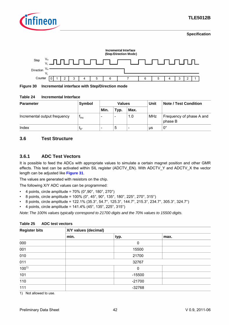
Figure 28 HS hysteresis
3.5.5 Incremental InterfaceThe Incremental Interface (IIF) uses an up/down counter of a microcontroller for the angle transmission. Thesynchronization is done by the parallel active SSC-Interface. The angle value read out by the SSC-Interface canbe compared with the stored counter value. In case of a non-synchronization, the microcontroller add thedifference to the actual counter value to synchronize the TLE5012B with the microcontroller. The resolution of theIIF can be selected within the interface mode4 register (MOD_4) under IFAB_RES. After startup the IIF pulses out the actual absolute angle value. So the microcontroller gets the information of theabsolute position. The Index-Signal which indicates the zero crossing is available on IFC pin.In register MOD_1 the incremental interface can be choosen between A/B mode and Step/Direction mode(IIF_MOD).Within the TLE5012B the incremental interface is implemented like a quadratur encoder with 50% duty cyle.
A/B ModeThe phase shift between phase A and B indicates a clockwise (A follows B) or a counterclockwise (B follows A)rotation of the magnet.
Figure 29 Incremental interface with A/B mode
Step/Direction ModePhase A pulses out the increments and phase B indicates the direction (Figure 30).
Ideal Switching Point
αelect
αHShystelαHShystel
αelect0°
90° el . Phase shift
0 1 2 3 4 5 6 7 6 5 4 3 2 1
Phase A
Counter
Phase B
Incremental Interface(A/B Mode)
VH
VL
VH
VL
TLE5012B
Specification
Preliminary Data Sheet 42 V 0.9, 2011-06
Figure 30 Incremental interface with Step/Direction mode
3.6 Test Structure
3.6.1 ADC Test VectorsIt is possible to feed the ADCs with appropriate values to simulate a certain magnet position and other GMReffects. This test can be activated within SIL register (ADCTV_EN). With ADCTV_Y and ADCTV_X the vectorlength can be adjusted like Figure 31.The values are generated with resistors on the chip.The following X/Y ADC values can be programmed:• 4 points, circle amplitude = 70% (0°,90°, 180°, 270°)• 8 points, circle amplitude = 100% (0°, 45°, 90°, 135°, 180°, 225°, 270°, 315°)• 8 points, circle amplitude = 122.1% (35.3°, 54.7°, 125.3°, 144.7°, 215.3°, 234.7°, 305.3°, 324.7°)• 4 points, circle amplitude = 141.4% (45°, 135°, 225°, 315°)Note: The 100% values typically correspond to 21700 digits and the 70% values to 15500 digits.
Table 24 Incremental InterfaceParameter Symbol Values Unit Note / Test Condition
Min. Typ. Max.Incremental output frequency fInc - - 1.0 MHz Frequency of phase A and
phase BIndex t0° - 5 - µs 0°
Table 25 ADC test vectorsRegister bits X/Y values (decimal)
min. typ. max.000 0001 15500010 21700011 327671001)
1) Not allowed to use.
0101 -15500110 -21700111 -32768
Step
Counter
Direction
Incremental Interface(Step /Direction Mode)
VH
VL
VH
VL
0 1 2 3 4 5 6 7 6 5 4 3 2 1

TLE5012B
Specification
Preliminary Data Sheet 43 V 0.9, 2011-06
Figure 31 ADC test vectors
Examples for ADC test vector checkThe sensor has to be selected first via CSQ and also SCK must be available for the communication. Table 26shows the structure of the communication to enable the ADC test vector for 54.7°.
Table 26 SSC Command to enable ADC test vector checkSSC Word No.
Description Master transmitting TLE5012 transmitting Note
1 Command 0_1010_0_000111_00012 Write Data 0_0_000_0_000_1_010_001 Check of 54.7°3 Safety Word 1_1_1_0_xxxx_xxxxxxxx
Table 27 Structure of Write Data for some different test vectorsSSC Word No.
Description Master transmitting TLE5012 transmitting Note
1 Write Data 0_0_000_0_000_1_001_101 ~135°2 Write Data 0_0_000_0_000_1_010_110 ~135°3 Write Data 0_0_000_0_000_1_101_110 ~215.3°4 Write Data 0_0_000_0_000_1_101_000 ~270°5 Write Data 0_0_000_0_000_1_101_010 ~324.7°
ADCTV_X
ADCTV_Y
0%
122.1%
100.0%
70%
141.4%

TLE5012B
Specification
Preliminary Data Sheet 44 V 0.9, 2011-06
3.7 Overvoltage ComparatorsVarious comparators monitor the voltage in order to ensure error free operation. The overvoltages must be activeat least 256 periods of tDIG to set the test comparator bits in the SSC Interface registers. This works as digital spikesuppression.
3.7.1 Internal Supply Voltage ComparatorsEvery voltage regulator has an overvoltage comparator to detect a malfunction. If the nominal output voltage of2.5 V is larger than VOVG, VOVA and VOVD, then this overvoltage comparator is activated.
Figure 32 OV comparator
3.7.2 VDD Overvoltage DetectionThe Overvoltage Detection Comparator monitors the external supply voltage at the VDD pin. It activates the S_VRbit.(Figure 32)
3.7.3 GND - Off ComparatorThe GND - Off Comparator is used to detect a voltage difference between the GND pin and SCK. It activates theS_VR bit of the SSC - Interface. This circuit can detect a disconnection of the Supply GND Pin.
Table 28 Test comparatorsParameter Symbol Values Unit Note / Test Condition
Min. Typ. Max.Overvoltage detection VOVG - 2.80 - V
VOVA - 2.80 - VVOVD - 2.80 - V
VDD overvoltage VDDOV - 6.05 - VVDD undervoltage VDDUV - 2.70 - VGND - off voltage VGNDoff - -0.55 - VVDD - off voltage VVDDoff - 0.55 - VSpike filter delay tDEL - 10 - µs
REF -
+
10µsSpikeFilter
xxx_OV
VDDA
GNDGND
VDDVRGVRAVRD

TLE5012B
Specification
Preliminary Data Sheet 45 V 0.9, 2011-06
Figure 33 GND - off comparator
3.7.4 VDD - Off ComparatorThe VDD - Off Comparator detects a disconnection of the VDD pin supply voltage. In this case, the TLE5012B issupplied by the SCK and CSQ input pins via the ESD structures. It activates the S_VR bit.
Figure 34 VDD - off comparator
-
+
10µsSpikeFilter
GND_OFF
VDDA
GND
SCK
GND
VDD
+dV
Diode-reference
1µsMonoFlop
10µsSpikeFilter
VDD_OFF
VDDA
GND
VDD
CSQSCK -dV
GND
1µsMonoFlop
-
+
VVDDoff

TLE5012B
Package Information
Preliminary Data Sheet 46 V 0.9, 2011-06
4 Package Information
4.1 Package Parameters
4.2 Package Outline
Figure 34 PG-DSO-8 package dimension
Table 29 Package ParametersParameter Symbol Limit Values Unit Notes
min. typ. max.Thermal Resistance RthJA - 150 200 K/W Junction to Air1)
1) according to Jedec JESD51-7
RthJC - - 75 K/W Junction to CaseRthJL - - 85 K/W Junction to Lead
Soldering Moisture Level MSL 3 260°CLead Frame CuPlating Sn 100% > 7 µm

TLE5012B
Package Information
Preliminary Data Sheet 47 V 0.9, 2011-06
Figure 35 Position of sensing element
4.3 Footprint
Figure 36 Footprint PG-DSO-8
4.4 Packing
Figure 37 Tape and Reel
0.65
1.31
5.69
1.27
8
6.4
5.2
0.3
±0.3
12
2.1
1.75

TLE5012B
Package Information
Preliminary Data Sheet 48 V 0.9, 2011-06
4.5 Marking
Processing
Note: For processing recommendations, please refer to Infineon’s Notes on processing
Position Marking Description1st Line 012Bxxxx See ordering table on Page 82nd Line xxx Lot code3rd Line Gxxxx G..green, 4-digit..date code

Published by Infineon Technologies AG
w w w . i n f i n e o n . c o m